CN102608699A - Short-range surface plasma waveguide and dielectric waveguide mixed coupling array type structure - Google Patents
Short-range surface plasma waveguide and dielectric waveguide mixed coupling array type structureDownload PDFInfo
- Publication number
- CN102608699A CN102608699ACN2012100091656ACN201210009165ACN102608699ACN 102608699 ACN102608699 ACN 102608699ACN 2012100091656 ACN2012100091656 ACN 2012100091656ACN 201210009165 ACN201210009165 ACN 201210009165ACN 102608699 ACN102608699 ACN 102608699A
- Authority
- CN
- China
- Prior art keywords
- short
- layer
- range surface
- surface plasma
- wave guide
- Prior art date
- Legal status (The legal status is an assumption and is not a legal conclusion. Google has not performed a legal analysis and makes no representation as to the accuracy of the status listed.)
- Granted
Links
Images


Landscapes
- Optical Integrated Circuits (AREA)
Abstract
Translated fromChinese
Description
Translated fromChinese技术领域technical field
本发明涉及光电子技术领域,具体涉及短程表面等离子体波导与介质波导混合耦合阵列式结构。The invention relates to the field of optoelectronic technology, in particular to a hybrid coupling array structure of a short-range surface plasmon waveguide and a dielectric waveguide.
背景技术Background technique
表面等离子体波(Surface plasmon polarition,SPP)是一种沿金属和介质界面传播的电磁场。如图1所示,1为金属(或金属和介质的混合物),2为金属周围的介质,3为一个界面处的表面等离子体波。Surface plasmon polarization (SPP) is an electromagnetic field that propagates along the interface between metal and medium. As shown in Figure 1, 1 is the metal (or a mixture of metal and medium), 2 is the medium around the metal, and 3 is the surface plasma wave at an interface.
当金属膜较薄时,上下表面等离子体波将发生耦合,生成两种新的表面等离子体波模式,见图2所示。其中一种模式为反对称模式,如图2中5所示,其模场较一般SPP波更趋附于金属,传播损耗较大,只能沿金属薄膜传播很短一段距离,被称为短程表面等离子体波(short range surface plasmon polarity,SRSPP)。当金属波导和介质波导距离足够近,在一定的条件下,介质波导模式将与SRSPP发生耦合。When the metal film is thinner, the upper and lower surface plasmon waves will be coupled to generate two new surface plasmon wave modes, as shown in Figure 2. One of the modes is the antisymmetric mode, as shown by 5 in Figure 2, its mode field is more attached to the metal than the general SPP wave, and the propagation loss is larger, and it can only propagate a short distance along the metal film, which is called the short-range surface Plasma waves (short range surface plasmon polarity, SRSPP). When the distance between the metal waveguide and the dielectric waveguide is close enough, under certain conditions, the dielectric waveguide mode will couple with the SRSPP.
由于SPP的场能量集中在金属和介质界面的附近,这使得在金属表面的场很强,对于表面的形态,特别是折射率的变化非常敏感,在生化传感器领域有广泛的应用前景。而短程SPP波较一般的SPP波,波场更加高度趋肤于金属表面,其模式特性对金属薄膜周围超薄范围内的介质折射率变化非常敏感,当金属膜上方超薄层物质的折射率发生变化时(大多数生物反应属于此类超薄层反应),短程表面等离子体波模式与介质波导模式的耦合将发生明显变化,从而引起介质波导输出功率的剧烈变化。这为实现超薄层物质折射率的高精度检测提供了新的途径。Since the field energy of SPP is concentrated near the interface between the metal and the medium, the field on the metal surface is very strong, and it is very sensitive to the surface morphology, especially the change of the refractive index, and has a wide application prospect in the field of biochemical sensors. Compared with the general SPP wave, the short-range SPP wave has a wave field that is more highly skin-like on the metal surface, and its mode characteristics are very sensitive to the change of the medium refractive index in the ultra-thin range around the metal film. When the refractive index of the ultra-thin layer material above the metal film When there is a change (most biological reactions belong to this kind of ultrathin layer reaction), the coupling between the short-range surface plasmon wave mode and the dielectric waveguide mode will change obviously, which will cause a drastic change in the output power of the dielectric waveguide. This provides a new way to achieve high-precision detection of the refractive index of ultra-thin layer materials.
传统的棱镜型表面等离子体波生化传感器体积大、调节困难,而且对超薄层物质探测灵敏度低,稳定性差,成本高,严重限制了其推广应用。而传统的波导型表面等离子体波生化传感器,也具有可传感范围较窄等问题。Traditional prism-type surface plasmon wave biochemical sensors are bulky, difficult to adjust, low sensitivity to ultra-thin layer substances, poor stability, and high cost, which seriously limit their popularization and application. The traditional waveguide-type surface plasmon wave biochemical sensor also has problems such as a narrow sensing range.
发明内容Contents of the invention
本发明的目的是提供一种短程表面等离子体波导与介质波导混合耦合阵列式结构,以实现超薄层介质折射率的可调传感范围实时检测,在保证高灵敏度、稳定性的同时,解决了传统的波导型表面等离子体波折射率检测方法传感范围小的问题。所述耦合结构包括:介质衬底层,以及位于介质衬底上的至少两个耦合结构。所述耦合结构包括:介质波导层,所述介质波导层位于所述介质衬底层上;以及短程表面等离子体波导层,所述短程表面等离子体波导层位于所述介质波导层上。其中,至少一个所述耦合结构的短程表面等离子体波导层与另一个所述耦合结构的短程表面等离子体波导层具有不同厚度。The purpose of the present invention is to provide a short-range surface plasmon waveguide and dielectric waveguide hybrid coupling array structure to realize the real-time detection of the adjustable sensing range of the refractive index of the ultra-thin layer medium, while ensuring high sensitivity and stability. The problem of the small sensing range of the traditional waveguide-type surface plasmon wave refractive index detection method is solved. The coupling structure includes: a dielectric substrate layer, and at least two coupling structures located on the dielectric substrate. The coupling structure includes: a dielectric waveguide layer located on the dielectric substrate layer; and a short-range surface plasmon waveguide layer located on the dielectric waveguide layer. Wherein, at least one of the peggeic surface plasmon waveguide layers of the coupling structure has a different thickness from that of the other coupling structure.
其中,至少一个所述耦合结构的介质波导层与另一个所述耦合结构的介质波导层具有不同宽度。Wherein, the dielectric waveguide layer of at least one coupling structure has a different width from the dielectric waveguide layer of another coupling structure.
其中,至少两个所述耦合结构具有相同厚度的短程表面等离子波导层和不同宽度的介质波导层。Wherein, at least two of the coupling structures have short-range surface plasmon waveguide layers with the same thickness and dielectric waveguide layers with different widths.
其中,至少一个所述耦合结构的短程表面等离子波导层与另一个所述耦合结构的短程表面等离子波导层具有相同厚度和不同长度。Wherein, the pegleg surface plasmon waveguide layer of at least one coupling structure has the same thickness and different lengths from the pegleg surface plasmon waveguide layer of another coupling structure.
其中,至少两个所述耦合结构的介质波导层具有同一输入端口和多个输出端口。进一步地,所述多个输出端口具有不同宽度。Wherein, the dielectric waveguide layers of at least two coupling structures have the same input port and multiple output ports. Further, the multiple output ports have different widths.
其中,至少一个所述耦合结构的短程表面等离子波导层与另一个所述耦合结构的短程表面等离子波导层具有相同厚度和不同长度。Wherein, the pegleg surface plasmon waveguide layer of at least one coupling structure has the same thickness and different lengths from the pegleg surface plasmon waveguide layer of another coupling structure.
其中,至少两个所述耦合结构的短程表面等离子体波导层彼此相连接。Wherein, the short-range surface plasmon waveguide layers of at least two coupling structures are connected to each other.
其中,所述耦合结构还包括位于所述短程表面等离子体波导层之上的介质覆盖层。进一步地,至少两个所述耦合结构的介质覆盖层彼此相连接。Wherein, the coupling structure further includes a dielectric covering layer located on the short-range surface plasmon waveguide layer. Further, the dielectric covering layers of at least two coupling structures are connected to each other.
其中,所述耦合结构还包括位于所述介质波导层之上、所述短程表面等离子体波导层之下的耦合匹配层。Wherein, the coupling structure further includes a coupling matching layer located above the dielectric waveguide layer and below the short-range surface plasmon waveguide layer.
其中,所述介质波导层的折射率大于所述衬底介质层的折射率,所述耦合匹配层的折射率小于所述介质波导层的折射率。Wherein, the refractive index of the dielectric waveguide layer is greater than the refractive index of the substrate dielectric layer, and the refractive index of the coupling matching layer is smaller than the refractive index of the dielectric waveguide layer.
其中,所述介质波导层的折射率的选择使得该介质波导TM偏振态的基模的等效折射率与该短程表面等离子体波的等效折射率相等。Wherein, the selection of the refractive index of the dielectric waveguide layer makes the equivalent refractive index of the fundamental mode of the TM polarization state of the dielectric waveguide equal to the equivalent refractive index of the short-range surface plasmon wave.
其中,所述介质波导层的折射率为1.2-3.8,所述介质波导层的厚度为10nm-5000nm,所述介质波导层宽度为2μm-20μm。Wherein, the refractive index of the dielectric waveguide layer is 1.2-3.8, the thickness of the dielectric waveguide layer is 10 nm-5000 nm, and the width of the dielectric waveguide layer is 2 μm-20 μm.
其中,所述耦合匹配层的厚度为0.01μm-10μm,所述耦合匹配层的折射率为1.2-3.8。Wherein, the thickness of the coupling matching layer is 0.01 μm-10 μm, and the refractive index of the coupling matching layer is 1.2-3.8.
其中,所述短程表面等离子体波导层为金属层,例如,为金、银、铝、铜、铁、铬、镍、钛中的一种或者几种组成的合金。Wherein, the short-range surface plasmon waveguide layer is a metal layer, for example, one or an alloy composed of gold, silver, aluminum, copper, iron, chromium, nickel, and titanium.
其中,所述短程表面等离子体波导层的厚度为10nm-100nm,所述短程表面等离子体波导层的长度为50μm-200μm。具有相同厚度的短程表面等离子体波导层所对应的介质波导可具有不同的宽度。Wherein, the thickness of the short-range surface plasmon waveguide layer is 10 nm-100 nm, and the length of the short-range surface plasmon waveguide layer is 50 μm-200 μm. The dielectric waveguides corresponding to the pegleg surface plasmon waveguide layers with the same thickness may have different widths.
其中,所述介质覆盖层的折射率为1.0-3.8。Wherein, the refractive index of the dielectric covering layer is 1.0-3.8.
其中,所述耦合匹配层厚度大于使介质波导与短程表面等离子体波耦合发生截止的临界厚度。Wherein, the thickness of the coupling matching layer is greater than the critical thickness for cutting off the coupling between the dielectric waveguide and the short-range surface plasmon wave.
其中,所述短程表面等离子波导层上除所述介质覆盖层外还可以设置有折射率待探测层。当折射率待探测层折射率发生变化时,介质波导TM模式和短程表面等离子体波的耦合效率发生改变,通过测定介质波导输出功率的变化来检测该短程表面等离子体波导层表面上方折射率待探测层折射率的变化。Wherein, besides the dielectric covering layer, a layer with a refractive index to be detected may be arranged on the short-range surface plasmon waveguide layer. When the refractive index of the layer to be detected changes, the coupling efficiency of the dielectric waveguide TM mode and the short-range surface plasmon wave changes, and the refractive index above the surface of the short-range surface plasmon waveguide layer is detected by measuring the change in the output power of the dielectric waveguide. Changes in the refractive index of the layer are detected.
其中,所述折射率待探测层折射率的微小变化包括由生物反应或是物理、化学作用引起的该折射率待探测层的折射率微小变化。Wherein, the small change in the refractive index of the layer to be detected includes a small change in the refractive index of the layer to be detected caused by a biological reaction or a physical or chemical action.
其中,通过调整所述短程表面等离子体波导层厚度可大范围调节所能探测的该折射率待探测层的折射率范围;通过调整所述介质波导宽度可小范围调节所能探测的该折射率待探测层的折射率范围。Wherein, by adjusting the thickness of the short-range surface plasmon waveguide layer, the range of the refractive index of the detectable layer to be detected can be adjusted in a large range; by adjusting the width of the dielectric waveguide, the detectable refractive index can be adjusted in a small range The refractive index range of the layer to be detected.
其中,所述传感器所能探测的折射率待探测层的厚度为所使用波长的1/15至500微米。Wherein, the thickness of the layer whose refractive index can be detected by the sensor is 1/15 to 500 microns of the wavelength used.
本发明所提供的短程表面等离子体波导与介质波导混合耦合阵列式结构,对于其中具有特定宽度的介质波导和特定厚度与长度的短程表面等离子体波导的垂直传感单元,传感中心的位置是确定的。典型地,该短程表面等离子体波导为金属波导。如果此时仅改变单元中介质波导的宽度,由于介质波导传播的介质模式传播常数的轻微改变,将导致传感中心位置出现轻微移动;如果仅改变单元中金属波导的厚度,由于金属波导传播的短程SPP模式传播常数的剧烈改变,将导致传感中心位置出现大范围的移动,此时,为了达到更好的能量耦合效果,金属波导长度(即耦合长度)也要进行相应改变。因此,在保证薄层物质折射率的高精度检测的同时,本专利解决了传统检测方法的体积大、调节困难、稳定性差、可检测范围小的问题。The short-range surface plasmon waveguide and dielectric waveguide hybrid coupling array structure provided by the present invention, for the vertical sensing unit with a dielectric waveguide of a specific width and a short-range surface plasmon waveguide of a specific thickness and length, the position of the sensing center is definite. Typically, the short-range surface plasmon waveguide is a metal waveguide. If only the width of the dielectric waveguide in the unit is changed at this time, the sensing center will move slightly due to the slight change of the propagation constant of the dielectric mode propagated by the dielectric waveguide; if only the thickness of the metal waveguide in the unit is changed, due to the The drastic change of the propagation constant of the short-range SPP mode will lead to a large-scale movement of the sensing center position. At this time, in order to achieve better energy coupling effect, the length of the metal waveguide (that is, the coupling length) should also be changed accordingly. Therefore, while ensuring high-precision detection of the refractive index of thin-layer materials, this patent solves the problems of large volume, difficult adjustment, poor stability, and small detectable range of traditional detection methods.
附图说明Description of drawings
图1和图2为表面等离子体波的概念图;Figure 1 and Figure 2 are conceptual diagrams of surface plasmon waves;
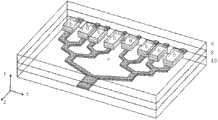
图3是短程表面等离子体波导与介质波导混合耦合阵列式结构的一个典型实施例的立体示意图;Fig. 3 is a three-dimensional schematic diagram of a typical embodiment of a hybrid coupling array structure of a short-range surface plasmon waveguide and a dielectric waveguide;
图4是图3的截面图;Fig. 4 is a sectional view of Fig. 3;
图5是本发明的短程表面等离子体波导与介质波导混合耦合阵列式传感结构的一个典型实施例的立体示意图;Fig. 5 is a three-dimensional schematic diagram of a typical embodiment of the short-range surface plasmon waveguide and dielectric waveguide hybrid coupling array sensing structure of the present invention;
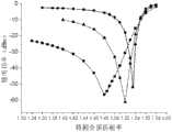
图6是本发明的短程表面等离子体波导与介质波导混合耦合阵列式传感结构的输出功率随待探测物质折射率的变化关系图;Fig. 6 is a graph showing the relationship between the output power of the short-range surface plasmon waveguide and the dielectric waveguide hybrid coupling array sensing structure as a function of the refractive index of the substance to be detected;
图7是短程表面等离子体波导与介质波导混合耦合阵列式传感结构的另一个典型实施例的立体示意图;Fig. 7 is a three-dimensional schematic diagram of another typical embodiment of a short-range surface plasmon waveguide and a dielectric waveguide hybrid coupling array sensing structure;
图8是短程表面等离子体波导与介质波导混合耦合阵列式传感结构另一个典型实施例的输出功率随待探测物质折射率的变化关系图;Fig. 8 is a graph showing the relationship between the output power and the refractive index of the substance to be detected in another typical embodiment of the short-range surface plasmon waveguide and dielectric waveguide hybrid coupling array sensing structure;
图9是短程表面等离子体波导与介质波导混合耦合阵列式传感结构的又一个典型实施例的立体示意图;Fig. 9 is a schematic perspective view of another typical embodiment of a short-range surface plasmon waveguide and dielectric waveguide hybrid coupling array sensing structure;
图10是短程表面等离子体波导与介质波导混合耦合阵列式传感结构又一个典型实施例的输出功率随待探测物质折射率的变化关系图;Fig. 10 is a graph showing the relationship between the output power and the refractive index of the substance to be detected in another typical embodiment of the short-range surface plasmon waveguide and dielectric waveguide hybrid coupling array sensing structure;
图11是短程表面等离子体波导与介质波导混合耦合阵列式传感结构的再一个典型实施例的立体示意图。Fig. 11 is a three-dimensional schematic diagram of yet another typical embodiment of a short-range surface plasmon waveguide and dielectric waveguide hybrid coupling array sensing structure.
图中:1、金属(或金属和介质的混合物);2、金属周围介质;3、界面处的表面等离子体波;4、长程表面等离子体波;5、短程表面等离子体波;6、短程表面等离子体波导层;7、介质波导层;8、耦合匹配层;9、介质覆盖层;10、介质衬底层;11、待探测物质层。In the figure: 1. Metal (or a mixture of metal and medium); 2. The medium surrounding the metal; 3. Surface plasmon waves at the interface; 4. Long-range surface plasmon waves; 5. Short-range surface plasmon waves; 6. Short-range surface plasmon waves Surface plasmon waveguide layer; 7. Dielectric waveguide layer; 8. Coupling matching layer; 9. Dielectric covering layer; 10. Dielectric substrate layer; 11. Substance layer to be detected.
具体实施方式Detailed ways
以下实施例用于说明本发明,但不用来限制本发明的范围。The following examples are used to illustrate the present invention, but are not intended to limit the scope of the present invention.
实施例1:Example 1:
图5所示为短程表面等离子体波导和介质波导混合耦合阵列式传感结构一实施例的结构图。在本实施例中,选择介质衬底层10的材料为SiO2,介质波导层7的材料为Si3N4,短程表面等离子体波导层6的材料为Au,介质覆盖层9的材料为SiO2,耦合匹配层8的材料为SiO2。在介质衬底层10上通过溅射或蒸镀和光刻的方法制作出宽度为2.5μm-5μm,180nm厚的Si3N4条7,一层1.5μm厚的SiO2耦合匹配层8后,在其上溅射一层15nm-30nm厚,长度为30μm-150μm的Au膜6,最后覆盖一层2μm的SiO2作为介质覆盖层9。短程表面等离子体波导层6(即金膜)6正上方除介质覆盖层9外还存在待探测物质层11,待探测物质层11的折射率随物理的(温度、湿度、压力、电磁场等)或生物、化学的因素(生化反应)发生变化时,从下边的介质臂耦合到上边金膜的能量将随着金膜6上方待探测物质11的折射率变化而发生变化。由于待探测物质层11的折射率将影响介质波导的TM模式和短程表面等离子体波之间的耦合,进而影响介质波导7的TM输出功率的大小,所以通过测定该介质波导7输出功率的变化可以检测该金膜6表面上方待探测物质11的折射率变化。所述待探测物质层11的折射率的微小变化可以是等效厚度的抗体、抗原等生物反应引起的,或是物理、化学等作用引起的该待探测物质层11的折射率微小变化。通过调整所述金膜6厚度可大范围调节所能探测的该待探测物质层11的折射率范围;通过调整所述介质波导宽度可小范围调节所能探测的该待探测物质层11的折射率范围。由于短程表面等离子体波模场高度趋附于金膜6表面,能够有效地感知金膜6周围较薄范围内的折射率变化,因此当待探测物质层11为一薄层物质时传感灵敏度依然很高,该待探测物质层11的厚度可薄至100nm以下。FIG. 5 is a structural diagram of an embodiment of a short-range surface plasmon waveguide and dielectric waveguide hybrid coupling array sensing structure. In this embodiment, the material of the
例如,当短程表面等离子体波导和介质波导混合耦合阵列式传感结构中某个传感单元中金膜6的厚度为22nm,长度为110μm,介质波导7的宽度为3.5μm,待探测物质层11厚度为300nm时,输入光波长为1550nm时,介质波导7的输入为0dB条件下,从介质波导7输出的功率Pout随待探测物质层11的折射率ndet变化的关系如图6中曲线F所示,可见,根据介质波导7的输出光强度的变化就可以获知待探测物质层11的折射率变化的信息,此时传感中心位置为1.448(黑线);而当介质波导7的宽度变为3μm和4μm,介质波导7传播的介质模式的传播常数出现轻微改变,因此传感中心分别移至1.445和1.451,可见传感中心随介质波导7的宽度出现轻微变化,如图6中曲线E和曲线G所示,进一步减小介质波导7的宽度到2.5μm时,传感中心进一步移动至1.442,如图6中曲线D所示;当改变金膜6的厚度为20nm,长度为100μm,介质波导7的宽度为3.5μm时,短程表面等离子体波导6(即金膜6)的传播的短程表面等离子体模式的传播常数发生剧烈变化,因此传感中心移至1.417,出现了大范围的移动,如图6中曲线B所示,此时继续改变介质波导7的宽度分别为3μm和4μm,传感中心出现轻微移动至1.413和1.42,分别如图6中曲线A和曲线C所示。于是,通过设计不同的金属膜厚度或介质波导宽度,可以大范围或精确地调整传感中心位置,解决了传统波导型SPP传感器件传感区域窄的问题。For example, when the thickness of the gold film 6 in a sensing unit in the short-range surface plasmon waveguide and dielectric waveguide hybrid coupling array sensing structure is 22 nm, the length is 110 μm, and the width of the dielectric waveguide 7 is 3.5 μm, the material layer to be detected When the thickness of 11 is 300nm, when the input light wavelength is 1550nm, and the input of the dielectric waveguide 7 is 0dB, the relationship between the output power Pout from the dielectric waveguide 7 and the change of the refractive index ndet of the material layer 11 to be detected is shown in Figure 6 As shown in the curve F, it can be seen that according to the change of the output light intensity of the dielectric waveguide 7, the information of the change in the refractive index of the material layer 11 to be detected can be obtained, and the sensing center position is 1.448 (black line); and when the dielectric waveguide 7 The width of the dielectric waveguide 7 becomes 3 μm and 4 μm, and the propagation constant of the dielectric mode propagated by the dielectric waveguide 7 changes slightly, so the sensing center moves to 1.445 and 1.451 respectively, and it can be seen that the sensing center changes slightly with the width of the dielectric waveguide 7, as shown in Figure 6 As shown in curve E and curve G, when the width of the dielectric waveguide 7 is further reduced to 2.5 μm, the sensing center further moves to 1.442, as shown in curve D in Figure 6; when the thickness of the gold film 6 is changed to 20nm, the length When the width of the dielectric waveguide 7 is 100 μm and the width of the dielectric waveguide 7 is 3.5 μm, the propagation constant of the short-range surface plasmon mode propagating in the short-range surface plasmon waveguide 6 (that is, the gold film 6) changes drastically, so the sensing center moves to 1.417, and a large The movement of the range, as shown by curve B in Figure 6, continues to change the width of the dielectric waveguide 7 to 3 μm and 4 μm, and the sensing center appears to move slightly to 1.413 and 1.42, respectively, as shown by curve A and curve C in Figure 6 Show. Therefore, by designing different metal film thicknesses or dielectric waveguide widths, the sensing center position can be adjusted in a large range or precisely, which solves the problem of narrow sensing areas of traditional waveguide-type SPP sensor devices.
根据本发明的各实施例,介质衬底层10可以是单一的介质衬底,也可以是其他类型衬底上形成的一层能起到衬底作用的介质层。介质衬底层10还可以是叠层结构,即根据需要由多种衬底以叠层或其他适当方式组合而成。According to various embodiments of the present invention, the
根据本发明的耦合阵列式结构包括位于介质衬底层10上的至少两个耦合结构,每个耦合结构都包括介质波导层7。各耦合结构的介质波导层7之间可以是独立的,即不互相连接,在各自入射端分别接收入射光源;也可以通过分光结构彼此存在连接关系,且存在连接关系的各介质波导层7拥有共同的入射端以接收入射光源。在后一种情况中,一种典型的连接实施例如说明书附图3所示,即各耦合结构的介质波导层7具有同一输入端口和多个输出端口。The coupled array structure according to the present invention includes at least two coupling structures located on the
耦合匹配层8是可选的,其作用在于提高介质波导7与短程表面等离子体波导层6之间的耦合效率,增强传感能力。因为介质波导7的TM模式和短程表面等离子体波导层6的短程表面等离子体模式之间的耦合效率决定于两个模式之间模场的交叠积分,两种模式的模场交叠面积越大而耦合效率就越高,所以耦合匹配层8厚度的选择将决定两种模式模场之间交叠积分的大小,从而进一步影响两个模式之间的耦合效率。The
介质覆盖层9也是可选的。介质覆盖层9的引入使得待探测物质层折射率的变化仅发生在短程表面等离子体波导6的正上方。因此,介质波导7的输入端和输出端的模场均不会受到待探测物质层11折射率变化的影响而发生模场泄露的现象,从而让检测结果更为准确。The
根据本发明的耦合阵列式结构包括位于介质衬底层10上的至少两个耦合结构,每个耦合结构都包括短程表面等离子体波导层6。本说明书附图3示出了各耦合结构的短程表面等离子体波导层6的一种实施方式。但本领域技术人员可以理解,各耦合结构的短程表面等离子体波导层6可以是如附图3所示的彼此断开的多个波导结构,也可以是彼此之间存在连接关系的结构,即形成连续的层结构,或者是若干个波导与层结构的适当组合。如果两个不同厚度的短程表面等离子体波导层6之间存是连续的,则其之间的过度可呈阶跃、阶梯或其他变化形式。但应注意到,如附图3所示的各耦合结构的短程表面等离子体波导层6的实施方式能带来好处,非连续的不同厚度的短程表面等离子波导层6具有有限的宽度,在工艺制作方面可通过光刻、刻蚀、溅射等工艺更好的控制厚度之间的阶跃。The coupled array structure according to the present invention includes at least two coupling structures on the
“短程表面等离子体波导层具有不同长度”,是指在入射光的传播方向上,某两个介质波导7上覆盖的短程表面等离子体波导层6延伸的长度不同。这包括短程表面等离子体波导层6是彼此断开的多个波导结构,或者是彼此连接的连续短程表面等离子体波导层结构这两种情况。"The short-range surface plasmon waveguide layers have different lengths" means that in the propagation direction of incident light, the extended lengths of the short-range surface plasmon waveguide layers 6 covered on two
与短程表面等离子体波导层6的情况类似,本说明书附图3也仅示出了位于短程表面等离子体波导层6之上的介质覆盖层9的一种实施方式。介质覆盖层9可以是如附图3所示的彼此断开的多个单独结构,也可以是彼此之间存在连接关系的结构,即形成连续的层结构,或者是若干个单独结构与层结构的适当组合。但应注意到,如附图3所示的各耦合结构的介质覆盖层9的实施方式能带来好处,在制作过程中,可通过等离子体增强化学气相沉积法或磁控溅射等半导体工艺在短程表面等离子体波导层6上方生长介质覆盖层,接着通过套刻、刻蚀等工艺即可简单的实现含短程等离子体波导层6上方的窗口的连续介质覆盖层9结构。Similar to the situation of the short-range surface plasmon waveguide layer 6 , FIG. 3 of this specification only shows an embodiment of the
根据本发明的一个实施例,至少一个所述耦合结构的短程表面等离子波导层6与另一个所述耦合结构的短程表面等离子波导层6具有相同厚度和不同长度。因为介质波导7的TM模式和短程表面等离子波导层6的短程表面等离子体模式之间的耦合效率与短程表面等离子体波导层6的长度有关。当短程表面等离子体波导层6的长度刚好等于耦合长度时,耦合效率最高,为了防止制作过程中出现的短程表面等离子体波导层6长度的工艺误差以及短程表面等离子波导层6厚度改变带来的耦合长度的变化,所以本发明中设计了不同长度的短程表面等离子体波导层6,使得器件的耦合和传感特性达到最佳。According to an embodiment of the present invention, at least one of the peggeic surface plasmon waveguiding layers 6 of the coupling structure has the same thickness and different lengths from the peggetic surface plasmon waveguide layer 6 of another coupling structure. Because the coupling efficiency between the TM mode of the
根据本发明的一个实施例,每一个所述介质波导层7的TM模式的等效折射率与对应的短程表面等离子体波导层6的短程表面等离子体波的等效折射率相等,所述耦合匹配层8的厚度大于使介质波导TM模式与短程表面等离子体波模式耦合发生截止的临界厚度。According to an embodiment of the present invention, the equivalent refractive index of the TM mode of each
当折射率待探测层11折射率发生变化时,介质波导层6的TM模式和短程表面等离子体波导层6的短程表面等离子体波的耦合效率发生改变,通过测定介质波导层7的输出功率的变化来检测所述折射率待探测层11折射率的变化。When the refractive index of the
通过调整所述短程表面等离子体波导层6厚度可大范围调节所能探测的该折射率待探测层11的折射率范围;通过调整所述介质波导层7的宽度可小范围调节所能探测的该折射率待探测层11的折射率范围。By adjusting the thickness of the short-range surface plasmon waveguide layer 6, the refractive index range of the detectable
实施例2:Example 2:
图7所示为短程表面等离子体波导和介质波导混合耦合阵列式传感结构的另一实施例的立体结构图。在本实施例中,选择介质衬底层10的材料为SiO2,介质波导层7的材料为Si3N4,短程表面等离子体波导层6的材料为Al,介质覆盖层9的材料为SiO2,耦合匹配层8的材料为SiO2。在介质衬底层10上通过溅射或蒸镀和光刻的方法制作出宽度为2.5μm-5μm,146nm厚的Si3N4条7,一层2μm厚的SiO2耦合匹配层8后,在其上溅射一层15nm-30nm厚Al膜6,最后覆盖一层3μm得SiO2作为介质覆盖层。入射波长为1550nm时,介质波导层7宽度分别为3μm,4μm,5μm,6μm时。待测介质层11的厚度仍为300nm,传播传方向长度为70μm。输出功率随被探测物的折射率变化如图8所示。此时传感中心降至1.35附近。FIG. 7 is a three-dimensional structure diagram of another embodiment of a hybrid coupling array sensing structure of a short-range surface plasmon waveguide and a dielectric waveguide. In this embodiment, the material of the
实施例3:Example 3:
又一个短程表面等离子体波导和介质波导混合耦合阵列式传感结构的例子如下所述。入射波长为850nm时,图9所示为短程表面等离子体波导和介质波导混合耦合阵列式传感结构又一实施例的结构图。选择介质衬底层10的材料为SiO2,介质波导层7的材料为PET(聚对苯二甲酸乙二酯),短程表面等离子体波导层6的材料为Au,介质覆盖层9的材料为SiO2,耦合匹配层8的材料为SiO2。在介质衬底层10上通过溅射或蒸镀和光刻的方法制作出宽度为10μm-15μm,1μm厚的有机材料PET条7,一层1.7μm厚的SiO2耦合匹配层8后,在其上溅射一层30nm-35nm厚Au膜6,最后覆盖一层2μm得SiO2作为介质覆盖层。当Au厚度为35nm时,待探测物质层11厚度为300nm时,根据介质覆盖层9的输出光强度的变化就可以获知待探测物质层11折射率变化的信息,此时传感中心位置为1.538,如图10中圆点曲线所示;而当将Au厚度改变为33nm时,传感中心移至1.52,同时探测动态范围增大,但灵敏度有所下降,如图10中三角曲线所示;继续减小Au厚度至30nm,传感中心继续向低折射率方向移动至1.48,如图10中方框曲线所示,且动态范围继续增大,灵敏度进一步下降。Another example of hybrid coupling array sensing structure of short-range surface plasmon waveguide and dielectric waveguide is as follows. When the incident wavelength is 850nm, FIG. 9 is a structural diagram of another embodiment of the hybrid coupling array sensing structure of the short-range surface plasmon waveguide and the dielectric waveguide. The material of the
实施例4:Example 4:
再一个短程表面等离子体波导和介质波导混合耦合阵列式传感结构的例子如下所述。入射光波长为633nm,图11所示为短程表面等离子体波导和介质波导混合耦合阵列式传感结构再一实施例的结构图。在本实施例中,衬底层10的材料选择为一种折射率为1.4的聚合物材料,介质波导层7的材料为Al2O3,短程表面等离子体波导层6的材料为Ag,介质覆盖层9的材料和耦合匹配层8的材料与衬底层10相同。在衬底上运用光刻及溅射或沉积的方法制作5μm-10μm宽、150nm厚的Al2O3条7。在Al2O3条上一层250nm厚的与介质衬底层10相同材料的聚合物作为耦合匹配层8并固化。随后15nm-20nm厚的Ag膜溅射于耦合匹配层之上,最后在Ag膜6上一层500nm厚的与介质衬底层10相同材料的聚合物作为介质覆盖层9并固化,Ag膜6上方除介质覆盖层9外还存在水体环境下的50nm厚的待探测物质层11,芯片传播传方向长度为50μm-100μm。在该探测波长更短,待探测物质层11更薄的情况下仍能获得高的灵敏度,相应的传感中心出现在1.37附近。传感芯片可采用CCD技术测试,如图11所示。Another example of a short-range surface plasmon waveguide and dielectric waveguide hybrid coupling array sensing structure is as follows. The wavelength of the incident light is 633nm. FIG. 11 is a structural diagram of another embodiment of the hybrid coupling array sensing structure of the short-range surface plasmon waveguide and the dielectric waveguide. In this embodiment, the material of the
上述实施例中短程表面等离子体波导层所使用的Al、Au、Ag等金属条可以换成铜、钛、镍、铬、铁中的任何一种或者是他们的合金,也可以是金属陶瓷条,即上述金属和合金和SiO2、MgF2、Al2O3、Si、GaAs、InP等介质的混合物。介质波导和介质衬底层、介质覆盖层的介质材料可换成树脂材料、SiO2、MgF2、Al2O3、Si、GaAs、InP等,但要求介质波导层的折射率大于周围介质的折射率。当改变材料时,短程表面等离子体波导层所使用的金属(或者金属陶瓷)条和介质波导层的几何参数要做一定的调整。The Al, Au, Ag and other metal strips used in the short-range surface plasmon waveguide layer in the above embodiments can be replaced by any one of copper, titanium, nickel, chromium, iron or their alloys, or cermet strips , that is, a mixture of the above metals and alloys and SiO2 , MgF2 , Al2 O3 , Si, GaAs, InP and other media. The dielectric material of the dielectric waveguide, the dielectric substrate layer, and the dielectric cover layer can be replaced by resin materials, SiO2 , MgF2 , Al2 O3 , Si, GaAs, InP, etc., but the refractive index of the dielectric waveguide layer is required to be greater than that of the surrounding medium Rate. When changing the material, the metal (or cermet) strips used in the short-range surface plasmon waveguide layer and the geometric parameters of the dielectric waveguide layer need to be adjusted to a certain extent.
以上实施方式仅用于说明本发明,而并非对本发明的限制,有关技术领域的普通技术人员,在不脱离本发明的精神和范围的情况下,还可以做出各种变化,因此所有等同的技术方案也属于本发明的范畴,本发明的专利保护范围应由其权利要求限定。The above embodiments are only used to illustrate the present invention, but not to limit the present invention. Those of ordinary skill in the relevant technical field can make various changes without departing from the spirit and scope of the present invention. Therefore, all equivalent The technical solution also belongs to the category of the present invention, and the scope of patent protection of the present invention should be defined by its claims.
Claims (20)
Priority Applications (1)
| Application Number | Priority Date | Filing Date | Title |
|---|---|---|---|
| CN201210009165.6ACN102608699B (en) | 2012-01-12 | 2012-01-12 | Short-range surface plasma waveguide and dielectric waveguide mixed coupling array type structure |
Applications Claiming Priority (1)
| Application Number | Priority Date | Filing Date | Title |
|---|---|---|---|
| CN201210009165.6ACN102608699B (en) | 2012-01-12 | 2012-01-12 | Short-range surface plasma waveguide and dielectric waveguide mixed coupling array type structure |
Publications (2)
| Publication Number | Publication Date |
|---|---|
| CN102608699Atrue CN102608699A (en) | 2012-07-25 |
| CN102608699B CN102608699B (en) | 2014-12-24 |
Family
ID=46526194
Family Applications (1)
| Application Number | Title | Priority Date | Filing Date |
|---|---|---|---|
| CN201210009165.6AActiveCN102608699B (en) | 2012-01-12 | 2012-01-12 | Short-range surface plasma waveguide and dielectric waveguide mixed coupling array type structure |
Country Status (1)
| Country | Link |
|---|---|
| CN (1) | CN102608699B (en) |
Cited By (4)
| Publication number | Priority date | Publication date | Assignee | Title |
|---|---|---|---|---|
| CN103267742A (en)* | 2013-04-19 | 2013-08-28 | 中国科学院半导体研究所 | Structures for Localized Surface Plasmon and Waveguide Mode Coupling |
| CN108051406A (en)* | 2018-02-02 | 2018-05-18 | 成都信息工程大学 | A kind of electrooptic effect fiber waveguide detection device |
| CN108303377A (en)* | 2018-02-02 | 2018-07-20 | 成都信息工程大学 | A kind of thermo-optic effect optical waveguide detection device |
| CN109407211A (en)* | 2018-11-30 | 2019-03-01 | 武汉邮电科学研究院有限公司 | A kind of waveguide component and divide bundling device |
Citations (2)
| Publication number | Priority date | Publication date | Assignee | Title |
|---|---|---|---|---|
| US6034809A (en)* | 1998-03-26 | 2000-03-07 | Verifier Technologies, Inc. | Optical plasmon-wave structures |
| CN101556353A (en)* | 2008-12-16 | 2009-10-14 | 清华大学 | Coupled structure of short-range surface plasma wave and media guided wave and application of same to sensor |
- 2012
- 2012-01-12CNCN201210009165.6Apatent/CN102608699B/enactiveActive
Patent Citations (2)
| Publication number | Priority date | Publication date | Assignee | Title |
|---|---|---|---|---|
| US6034809A (en)* | 1998-03-26 | 2000-03-07 | Verifier Technologies, Inc. | Optical plasmon-wave structures |
| CN101556353A (en)* | 2008-12-16 | 2009-10-14 | 清华大学 | Coupled structure of short-range surface plasma wave and media guided wave and application of same to sensor |
Non-Patent Citations (2)
| Title |
|---|
| BOYU FAN ET AL.: "Hybrid Coupler with Short Range Surface Plasmon Polarition and Dielectric Waveguide", 《SPIE-OSA-IEEE ASIA COMMUNICATIONS AND PHOTONICS》* |
| RUIYUAN WAN ET AL.: "Ultrathin layer sensing based on hybrid coupler with short-range surface plasmon polariton and dielectric waveguide", 《OPTICS LETTERS》* |
Cited By (7)
| Publication number | Priority date | Publication date | Assignee | Title |
|---|---|---|---|---|
| CN103267742A (en)* | 2013-04-19 | 2013-08-28 | 中国科学院半导体研究所 | Structures for Localized Surface Plasmon and Waveguide Mode Coupling |
| CN108051406A (en)* | 2018-02-02 | 2018-05-18 | 成都信息工程大学 | A kind of electrooptic effect fiber waveguide detection device |
| CN108303377A (en)* | 2018-02-02 | 2018-07-20 | 成都信息工程大学 | A kind of thermo-optic effect optical waveguide detection device |
| CN108051406B (en)* | 2018-02-02 | 2023-05-09 | 成都信息工程大学 | An electro-optic effect optical waveguide detection device |
| CN108303377B (en)* | 2018-02-02 | 2023-05-09 | 成都信息工程大学 | A thermo-optic effect optical waveguide detection device |
| CN109407211A (en)* | 2018-11-30 | 2019-03-01 | 武汉邮电科学研究院有限公司 | A kind of waveguide component and divide bundling device |
| CN109407211B (en)* | 2018-11-30 | 2021-03-02 | 武汉邮电科学研究院有限公司 | Waveguide element and beam splitter |
Also Published As
| Publication number | Publication date |
|---|---|
| CN102608699B (en) | 2014-12-24 |
Similar Documents
| Publication | Publication Date | Title |
|---|---|---|
| CN101246123B (en) | Long-range surface plasma wave refractive index detecting chip | |
| US8358880B2 (en) | Hybrid coupling structure of the short range plasmon polariton and conventional dielectric waveguide, a coupling structure of the long range plasmon polariton and conventional dielectric waveguide, and applications thereof | |
| CN110133771B (en) | Method for realizing ultra-narrow band absorption and sensing by using structural symmetry defects | |
| Ji et al. | Surface plasmon resonance refractive index sensor based on ultraviolet bleached polymer waveguide | |
| CN101581814A (en) | Coupling Structure of Long Range Surface Plasmon Wave and Dielectric Guided Wave and Its Application | |
| CN102608699A (en) | Short-range surface plasma waveguide and dielectric waveguide mixed coupling array type structure | |
| CN102062729A (en) | Integrated structure of micro-ring cavity structure-based two-channel sensors and microfluidic channels and manufacture method of integrated structure | |
| CN108802468A (en) | Photonic crystal fiber electromagnetism dual sampling device | |
| CN109001157A (en) | A method of refractive index sensing is realized based on duplex surface plasma resonance | |
| CN101556353B (en) | Coupled structure of short-range surface plasma wave and media guided wave and application of same to sensor | |
| Maurya et al. | Influence of adhesion layer on performance of surface plasmon resonance sensor | |
| CN104634763B (en) | A kind of SPR sensorgram chip and preparation method thereof | |
| Das et al. | A theoretical insight into the use of anti-reflective coatings for the upliftment of sensitivity of surface plasmon resonance sensors | |
| Kumar et al. | Long-range surface plasmon resonance biosensors with cytop/Al/Perovskite and cytop/Al/MoS2 configurations | |
| Singh et al. | High-performance plasmonic biosensor for blood cancer detection: achieving ultrahigh figure-of-merit | |
| Li et al. | Magneto-optical properties and sensing performance of one-dimensional all-metal magnetic nanogratings | |
| Liu et al. | Ge2Sb2Te5-coated fiber optic SPR sensor: Improving sensitivity | |
| CN100582830C (en) | Mixed three-arm long-distance surface plasma waveguide and media waveguide coupling device | |
| CN104089931A (en) | High-sensitivity refractive index sensor based on medium magneto-optical surface plasma resonance | |
| CN103900991A (en) | Refractive index sensor based on surface plasmon resonance | |
| CN114778493A (en) | Plasmon resonance sensor with ordered arrangement of nanoparticles and method for making the same | |
| Tarumaraja et al. | FDTD numerical analysis of SPR sensing using graphene-based photonic crystal | |
| Sheng et al. | Optimization of tunable symmetric SPR sensor based on Ag-graphene | |
| Lu et al. | Waveguide-coupled surface plasmon resonance sensor for both liquid and gas detections | |
| CN102393380A (en) | Surface plasma resonance sensor |
Legal Events
| Date | Code | Title | Description |
|---|---|---|---|
| C06 | Publication | ||
| PB01 | Publication | ||
| C10 | Entry into substantive examination | ||
| SE01 | Entry into force of request for substantive examination | ||
| C14 | Grant of patent or utility model | ||
| GR01 | Patent grant |