CN102544069B - Tunneling transistor with horizontal alignment coaxial cable structure and method for forming tunneling transistor - Google Patents
Tunneling transistor with horizontal alignment coaxial cable structure and method for forming tunneling transistorDownload PDFInfo
- Publication number
- CN102544069B CN102544069BCN201210035540.4ACN201210035540ACN102544069BCN 102544069 BCN102544069 BCN 102544069BCN 201210035540 ACN201210035540 ACN 201210035540ACN 102544069 BCN102544069 BCN 102544069B
- Authority
- CN
- China
- Prior art keywords
- region
- source region
- drain region
- type
- semiconductor body
- Prior art date
- Legal status (The legal status is an assumption and is not a legal conclusion. Google has not performed a legal analysis and makes no representation as to the accuracy of the status listed.)
- Expired - Fee Related
Links
Images


Landscapes
- Thin Film Transistor (AREA)
Abstract
Translated fromChinese
Description
Translated fromChinese技术领域technical field
本发明涉及半导体设计和制造技术领域,特别涉及一种具有水平准同轴电缆结构的隧穿晶体管及其形成方法。The invention relates to the technical field of semiconductor design and manufacture, in particular to a tunneling transistor with a horizontal quasi-coaxial cable structure and a forming method thereof.
背景技术Background technique
长期以来,为了获得更高的芯片密度、更快的工作速度以及更低的功耗。金属-氧化物-半导体场效应晶体管(MOSFET)的特征尺寸一直遵循着所谓的摩尔定律(Moore’slaw)不断按比例缩小,其工作速度越来越快。当前已经进入到了纳米尺度的范围。然而,随之而来的一个严重的挑战是出现了短沟道效应,例如亚阈值电压下跌(Vtroll-off)、漏极引起势垒降低(DIBL)、源漏穿通(punch through)等现象,使得器件的关态泄漏电流显著增大,从而导致性能发生恶化。For a long time, in order to obtain higher chip density, faster working speed and lower power consumption. The feature size of Metal-Oxide-Semiconductor Field Effect Transistors (MOSFETs) has been continuously scaling down in accordance with the so-called Moore's law, and their operating speeds are getting faster and faster. At present, it has entered the range of nanoscale. However, a serious challenge that comes with it is the short channel effect, such as subthreshold voltage drop (Vtroll-off), drain-induced barrier lowering (DIBL), source-drain punch through, etc. The off-state leakage current of the device is significantly increased, resulting in performance degradation.
当前,为了减小短沟道效应带来的负面影响,人们提出了各种各样的改进措施,其中尤为突出的是隧穿场效应晶体管(tunneling field effect transistor,TFET)。由于MOSFET器件处在亚阈值状态时,器件为弱反型,此时热电子发射为主要的导电机制,因此,在室温下MOSFET的亚阈值斜率受限于60mV/dec。相对于传统的MOSFET而言,一方面,因为隧穿场效应晶体管器件的有源区本质上为隧穿结,因此,隧穿场效应晶体管具有更弱的甚至没有短沟道效应;同时,隧穿场效应晶体管的主要电流机制为带-带隧穿(band-to-band tunneling),在亚阈值区以及饱和区漏极电流与外加的栅源电压呈指数关系,因此隧穿场效应晶体管具有更低的亚阈值斜率,并且电流几乎不受温度的影响。At present, in order to reduce the negative impact brought by the short channel effect, various improvement measures have been proposed, among which the tunneling field effect transistor (Tunneling field effect transistor, TFET) is the most prominent. Since the MOSFET device is in the subthreshold state, the device is weak inversion, and thermionic emission is the main conduction mechanism at this time. Therefore, the subthreshold slope of the MOSFET is limited to 60mV/dec at room temperature. Compared with the traditional MOSFET, on the one hand, because the active region of the tunneling field effect transistor device is essentially a tunneling junction, the tunneling field effect transistor has weaker or even no short channel effect; at the same time, the tunneling field effect transistor The main current mechanism of the field effect transistor is band-to-band tunneling. In the subthreshold region and saturation region, the drain current has an exponential relationship with the applied gate-source voltage, so the tunneling field effect transistor has Lower subthreshold slope, and the current is almost independent of temperature.
隧穿场效应晶体管的制备工艺与传统的互补型金属-氧化物-半导体场效应晶体管(CMOSFET)工艺相兼容。TFET晶体管的结构是基于金属-氧化物-半导体栅控的p-i-n二极管,如图1所示,为现有技术中一个典型的n型沟道TFET。具体地,N型沟道TFET包含一个P型掺杂的源区1000’和一个N型掺杂的漏区2000’,源区和漏区之间被一个沟道区3000’所隔离开,栅堆叠4000’包含一个位于沟道区上方的栅介质层和一个栅电极。The fabrication process of the tunneling field effect transistor is compatible with the traditional complementary metal-oxide-semiconductor field effect transistor (CMOSFET) process. The structure of the TFET transistor is based on a metal-oxide-semiconductor gate-controlled p-i-n diode, as shown in FIG. 1 , which is a typical n-channel TFET in the prior art. Specifically, the N-type channel TFET includes a P-type doped source region 1000' and an N-type doped drain region 2000', the source region and the drain region are separated by a channel region 3000', and the gate The stack 4000' includes a gate dielectric layer and a gate electrode over the channel region.
在TFET器件的关闭状态,即没有施加栅压时,源区1000’和漏区2000’之间形成的结为反向偏置的二极管,而由反向偏置二极管建立的势垒大于通常互补型MOSFET所建立的势垒,因此,这就导致了即使沟道长度非常短的时候TFET器件的亚阈值泄漏电流和直接隧穿电流大大降低。当对TFET的栅极施加电压,在场效应的作用下器件的沟道区3000’产生一个电子的通道,一旦沟道中的电子浓度发生简并,那么在源区1000’和沟道区3000’之间就会形成一个隧穿结,隧穿产生的隧穿电流通过这个隧穿结。从能带的角度来看,这种基于栅控P-I-N二极管结构的隧穿场效应晶体管是通过控制栅极电压来调节源区1000’和沟道区3000’之间所形成的PN结的隧道长度。In the off state of the TFET device, that is, when no gate voltage is applied, the junction formed between the source region 1000' and the drain region 2000' is a reverse-biased diode, and the potential barrier established by the reverse-biased diode is larger than the usual complementary The potential barrier established by the type MOSFET, therefore, leads to a greatly reduced subthreshold leakage current and direct tunneling current of the TFET device even when the channel length is very short. When a voltage is applied to the gate of the TFET, the channel region 3000' of the device generates an electron channel under the action of the field effect. Once the electron concentration in the channel degenerates, the source region 1000' and the channel region 3000' A tunneling junction will be formed between them, and the tunneling current generated by the tunneling will pass through the tunneling junction. From the point of view of the energy band, this tunneling field effect transistor based on the gated P-I-N diode structure adjusts the tunnel length of the PN junction formed between the source region 1000' and the channel region 3000' by controlling the gate voltage .
现有的水平隧穿的TFET器件的缺点在于:由于水平隧穿的截面积较小,导致驱动电流过小,影响TFET器件的驱动性能。The disadvantage of the existing horizontal tunneling TFET device is that: due to the small cross-sectional area of the horizontal tunneling, the driving current is too small, which affects the driving performance of the TFET device.
发明内容Contents of the invention
本发明的目的旨在至少解决上述技术缺陷之一,特别是解决或避免出现TFET器件的上述缺点。The object of the present invention is to solve at least one of the above-mentioned technical defects, especially to solve or avoid the above-mentioned defects of TFET devices.
为达到上述目的,本发明一方面提出一种具有水平准同轴电缆结构的隧穿晶体管,包括:半导体衬底;形成在所述半导体衬底上的源区或漏区,其中,所述源区或漏区具有第一掺杂类型,所述半导体衬底上未形成所述源区或漏区的区域形成有绝缘层;半导体体区,所述半导体体区的第一部分包覆所述源区或漏区的第一部分表面形成沟道区,所述半导体体区的第二部分位于所述绝缘层上且具有第二掺杂类型,所述半导体体区的第二部分为漏区或源区;形成在所述沟道区上的栅结构,所述栅结构包覆所述沟道区。To achieve the above object, the present invention proposes a tunneling transistor with a horizontal quasi-coaxial cable structure, comprising: a semiconductor substrate; a source region or a drain region formed on the semiconductor substrate, wherein the source A region or a drain region has a first doping type, and an insulating layer is formed on a region where the source region or drain region is not formed on the semiconductor substrate; a semiconductor body region, a first part of the semiconductor body region covers the source A first part of the surface of the region or drain region forms a channel region, a second part of the semiconductor body region is located on the insulating layer and has a second doping type, and the second part of the semiconductor body region is a drain region or a source region; a gate structure formed on the channel region, the gate structure wrapping the channel region.
在本发明的一个实施例中,所述源区或漏区为形成在所述半导体衬底上的半导体纳米线或纳米带。通过生长纳米线或纳米带形成的漏区或源区可以进一步在其上形成双栅或环栅(gate-all-around)结构,有利于增加栅对沟道区的控制能力,提高有效电场,增加隧穿概率。In one embodiment of the present invention, the source region or the drain region is a semiconductor nanowire or a nanoribbon formed on the semiconductor substrate. The drain or source region formed by growing nanowires or nanobelts can further form a double gate or gate-all-around structure on it, which is beneficial to increase the control ability of the gate to the channel region and improve the effective electric field. Increased tunneling probability.
在本发明的一个实施例中,所述源区或漏区的材料包括:Ge、SiGe、应变Si或者III-V族材料中的一种。这些半导体材料不仅可以形成异质结,而且禁带宽度小,有利于增大TFET的隧穿概率。In one embodiment of the present invention, the material of the source region or the drain region includes one of Ge, SiGe, strained Si or III-V group materials. These semiconductor materials can not only form heterojunctions, but also have a small forbidden band width, which is conducive to increasing the tunneling probability of TFETs.
在本发明的一个实施例中,所述半导体体区为在所述源区或漏区的第一部分表面以及所述绝缘层上外延形成,从而可以使所述沟道区的厚度小于10nm,以有效地减小TFET的隧穿路径。In one embodiment of the present invention, the semiconductor body region is epitaxially formed on the first part of the surface of the source region or the drain region and the insulating layer, so that the thickness of the channel region can be made less than 10 nm, so that Effectively reduce the tunneling path of TFET.
在本发明的一个实施例中,所述源区或漏区为P型重掺杂,所述沟道区为P型弱掺杂、N型弱掺杂或者本征,所述漏区或源区为N型重掺杂;或者,所述源区或漏区为N型重掺杂,所述沟道区为N型弱掺杂、P型弱掺杂或者本征,所述漏区或源区为P型重掺杂。其中,当源区为P型重掺杂,沟道区为P型弱掺杂、N型弱掺杂或者本征,漏区为N型重掺杂时,构成N型隧穿场效应晶体管;当源区为N型重掺杂,沟道区为P型弱掺杂、N型弱掺杂或者本征,漏区为P型重掺杂时,构成P型隧穿场效应晶体管。In one embodiment of the present invention, the source region or the drain region is P-type heavily doped, the channel region is P-type weakly doped, N-type weakly doped or intrinsic, and the drain region or source The region is N-type heavily doped; or, the source region or the drain region is N-type heavily doped, the channel region is N-type weakly doped, P-type weakly doped or intrinsic, and the drain region or The source region is heavily doped P-type. Wherein, when the source region is P-type heavily doped, the channel region is P-type weakly doped, N-type weakly doped or intrinsic, and the drain region is N-type heavily doped, an N-type tunneling field effect transistor is formed; When the source region is N-type heavily doped, the channel region is P-type weakly doped, N-type weakly doped or intrinsic, and the drain region is P-type heavily doped, a P-type tunneling field effect transistor is formed.
本发明另一方面还提出一种具有水平准同轴电缆结构的隧穿晶体管的形成方法,包括以下步骤:提供半导体衬底;在所述半导体衬底上形成源区或漏区,对所述源区或漏区进行第一类型掺杂;在所述半导体衬底上未形成所述源区或漏区的区域形成绝缘层;在所述源区或漏区的第一部分以及所述绝缘层上形成半导体体区,所述半导体体区的第一部分包覆所述源区或漏区的第一部分形成沟道区,对形成在所述绝缘层上的所述半导体体区的第二部分进行第二类型掺杂以形成漏区或源区;在所述沟道区上形成包覆所述沟道区的栅结构。Another aspect of the present invention also proposes a method for forming a tunneling transistor with a horizontal quasi-coaxial cable structure, including the following steps: providing a semiconductor substrate; forming a source region or a drain region on the semiconductor substrate; The source region or the drain region is doped with the first type; an insulating layer is formed in a region where the source region or the drain region is not formed on the semiconductor substrate; the first part of the source region or the drain region and the insulating layer are A semiconductor body region is formed on the insulating layer, the first part of the semiconductor body region covers the first part of the source region or the drain region to form a channel region, and the second part of the semiconductor body region formed on the insulating layer is second type doping to form a drain region or a source region; forming a gate structure covering the channel region on the channel region.
在本发明的一个实施例中,形成所述源区或漏区包括:在所述半导体衬底上生长半导体纳米线或纳米带,以形成所述源区或漏区。通过生长纳米线或纳米带形成的源区或漏区可以进一步在其上形成双栅或环栅(gate-all-around)结构,有利于增加栅对沟道区的控制能力,提高有效电场,增加隧穿概率。In one embodiment of the present invention, forming the source region or the drain region includes: growing semiconductor nanowires or nanobelts on the semiconductor substrate to form the source region or the drain region. The source or drain region formed by growing nanowires or nanobelts can further form a double gate or gate-all-around structure on it, which is conducive to increasing the control ability of the gate to the channel region and improving the effective electric field. Increased tunneling probability.
在本发明的一个实施例中,所述源区或漏区的材料包括:Ge、SiGe、应变Si或者III-V族材料。这些半导体材料不仅可以形成异质结,而且禁带宽度小,有利于增大TFET的隧穿概率。In one embodiment of the present invention, the material of the source region or the drain region includes: Ge, SiGe, strained Si or III-V group materials. These semiconductor materials can not only form heterojunctions, but also have a small forbidden band width, which is conducive to increasing the tunneling probability of TFETs.
在本发明的一个实施例中,形成所述沟道区以及漏区或源区包括:在所述源区或漏区和绝缘层上外延生长半导体体区层;根据预设图案刻蚀所述半导体体区层以形成半导体体区,使得所述半导体体区的第一部分包覆所述源区或漏区的第一部分形成沟道区,所述半导体体区的第二部分形成在所述绝缘层上;对所述半导体体区的第二部分进行第二类型掺杂以形成漏区或源区。通过外延生长形成的沟道区的厚度可以达到小于10nm,从而可以有效地减小TFET的隧穿路径。In one embodiment of the present invention, forming the channel region and the drain region or source region includes: epitaxially growing a semiconductor body layer on the source region or drain region and the insulating layer; etching the a semiconductor body region layer to form a semiconductor body region, so that the first part of the semiconductor body region covers the first part of the source region or the drain region to form a channel region, and the second part of the semiconductor body region is formed on the insulating layer; doping a second portion of the semiconductor body region with a second type to form a drain region or a source region. The thickness of the channel region formed by epitaxial growth can reach less than 10 nm, so that the tunneling path of the TFET can be effectively reduced.
在本发明的一个实施例中,形成所述栅结构包括:氧化所述半导体体区以形成氧化层;根据预设图案刻蚀所述氧化层,以在所述沟道区上形成栅介质层。在本发明的一个可选的实施例中,形成所述栅结构包括:在所述半导体体区上形成高介电常数介质层;根据预设图案刻蚀所述高介电常数介质层,以在所述沟道区上形成栅介质层。通过上述两种方式形成的栅介质层均可以达到等效氧化层厚度EOT小于1nm。In one embodiment of the present invention, forming the gate structure includes: oxidizing the semiconductor body region to form an oxide layer; etching the oxide layer according to a preset pattern to form a gate dielectric layer on the channel region . In an optional embodiment of the present invention, forming the gate structure includes: forming a high dielectric constant dielectric layer on the semiconductor body region; etching the high dielectric constant dielectric layer according to a preset pattern to A gate dielectric layer is formed on the channel region. The gate dielectric layer formed by the above two methods can achieve an equivalent oxide layer thickness EOT of less than 1 nm.
在本发明的一个实施例中,形成所述栅介质层之后还包括:在所述栅介质层上形成栅电极,在所述源区或漏区上形成第一电极,以及在所述漏区或源区上形成第二电极。其中,第一电极即为源电极或漏电极,第二电极即相应地为漏电极或源电极。In one embodiment of the present invention, after forming the gate dielectric layer, it further includes: forming a gate electrode on the gate dielectric layer, forming a first electrode on the source region or the drain region, and forming a first electrode on the drain region Or form a second electrode on the source region. Wherein, the first electrode is the source electrode or the drain electrode, and the second electrode is the drain electrode or the source electrode accordingly.
在本发明的一个实施例中,形成所述源区、漏区和沟道区包括:对所述源区或漏区进行N型重掺杂,对所述沟道区进行P型弱掺杂、N型弱掺杂或者本征,对所述漏区或源区进行P型重掺杂及;或者对所述源区或漏区进行P型重掺杂,对所述沟道区进行P型弱掺杂、N型弱掺杂或者本征,对所述漏区或源区进行N型重掺杂。In one embodiment of the present invention, forming the source region, the drain region and the channel region includes: performing N-type heavy doping on the source region or the drain region, and performing P-type weak doping on the channel region , N-type weak doping or intrinsic, carry out P-type heavy doping to the drain region or source region; or carry out P-type heavy doping to the source region or drain region, and carry out P-type doping to the channel region N-type weak doping, N-type weak doping or intrinsic, N-type heavy doping is performed on the drain region or source region.
本发明提供一种具有水平准同轴电缆结构的隧穿晶体管及其形成方法,通过将沟道区、源/漏区、栅结构设置成在具有水平方向同轴电缆的结构,从源区到沟道区的环状隧穿截面相对于普通的平面隧穿截面,隧穿截面积大大增加,栅对沟道区的控制能力显著增强,从而改善TFET器件的驱动能力。另外,由于根据本发明实施例的隧穿晶体管为形成在衬底上的水平结构,故其制造方法可以与现有的水平结构的半导体制造技术兼容,且有利于半导体器件的集成。The present invention provides a tunneling transistor with a horizontal quasi-coaxial cable structure and its forming method. By arranging the channel region, source/drain region, and gate structure in a structure with a horizontal coaxial cable, from the source region to the Compared with the ordinary planar tunneling section, the annular tunneling section of the channel region has a greatly increased tunneling section area, and the control ability of the gate to the channel area is significantly enhanced, thereby improving the driving ability of the TFET device. In addition, since the tunneling transistor according to the embodiment of the present invention is a horizontal structure formed on the substrate, its manufacturing method can be compatible with the existing semiconductor manufacturing technology of the horizontal structure, and is beneficial to the integration of semiconductor devices.
本发明附加的方面和优点将在下面的描述中部分给出,部分将从下面的描述中变得明显,或通过本发明的实践了解到。Additional aspects and advantages of the invention will be set forth in part in the description which follows, and in part will be obvious from the description, or may be learned by practice of the invention.
附图说明Description of drawings
本发明上述的和/或附加的方面和优点从下面结合附图对实施例的描述中将变得明显和容易理解,其中:The above and/or additional aspects and advantages of the present invention will become apparent and easy to understand from the following description of the embodiments in conjunction with the accompanying drawings, wherein:
图1为现有技术中一个典型的n型隧穿场效应晶体管结构图;FIG. 1 is a structural diagram of a typical n-type tunneling field effect transistor in the prior art;
图2为本发明实施例的具有水平准同轴电缆结构的TFET结构的俯视图;2 is a top view of a TFET structure with a horizontal quasi-coaxial cable structure according to an embodiment of the present invention;
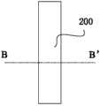
图3-5分别为沿图2所示的具有水平准同轴电缆结构的TFET结构的俯视图中的线AA’、BB’、CC’的剖面图;Fig. 3-5 is respectively along the sectional view of line AA ', BB ', CC ' in the plan view of the TFET structure with horizontal quasi-coaxial cable structure shown in Fig. 2;
图6-15为本发明实施例的具有水平准同轴电缆结构的TFET结构的形成方法各步骤的结构剖面图。6-15 are structural cross-sectional views of each step of the method for forming a TFET structure with a horizontal quasi-coaxial cable structure according to an embodiment of the present invention.
具体实施方式Detailed ways
下面详细描述本发明的实施例,所述实施例的示例在附图中示出,其中自始至终相同或类似的标号表示相同或类似的元件或具有相同或类似功能的元件。下面通过参考附图描述的实施例是示例性的,仅用于解释本发明,而不能解释为对本发明的限制。Embodiments of the present invention are described in detail below, examples of which are shown in the drawings, wherein the same or similar reference numerals designate the same or similar elements or elements having the same or similar functions throughout. The embodiments described below by referring to the figures are exemplary only for explaining the present invention and should not be construed as limiting the present invention.
下文的公开提供了许多不同的实施例或例子用来实现本发明的不同结构。为了简化本发明的公开,下文中对特定例子的部件和设置进行描述。当然,它们仅仅为示例,并且目的不在于限制本发明。此外,本发明可以在不同例子中重复参考数字和/或字母。这种重复是为了简化和清楚的目的,其本身不指示所讨论各种实施例和/或设置之间的关系。此外,本发明提供了的各种特定的工艺和材料的例子,但是本领域普通技术人员可以意识到其他工艺的可应用于性和/或其他材料的使用。另外,以下描述的第一特征在第二特征之“上”的结构可以包括第一和第二特征形成为直接接触的实施例,也可以包括另外的特征形成在第一和第二特征之间的实施例,这样第一和第二特征可能不是直接接触。The following disclosure provides many different embodiments or examples for implementing different structures of the present invention. To simplify the disclosure of the present invention, components and arrangements of specific examples are described below. Of course, they are only examples and are not intended to limit the invention. Furthermore, the present invention may repeat reference numerals and/or letters in different instances. This repetition is for the purpose of simplicity and clarity and does not in itself indicate a relationship between the various embodiments and/or arrangements discussed. In addition, various specific process and material examples are provided herein, but one of ordinary skill in the art will recognize the applicability of other processes and/or the use of other materials. Additionally, configurations described below in which a first feature is "on" a second feature may include embodiments where the first and second features are formed in direct contact, and may include additional features formed between the first and second features. For example, such that the first and second features may not be in direct contact.
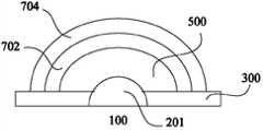
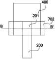
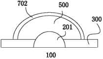
图2为本发明实施例的具有水平准同轴电缆结构的TFET的结构俯视图,图3-5分别为沿图2中的线AA’、BB’、CC’的剖面图。如图2-5所示,根据本发明实施例的具有水平准同轴电缆结构的TFET包括:半导体衬底100;形成在半导体衬底100上的具有第一掺杂类型的源区或漏区200,其中,半导体衬底100上未形成源区或漏区200的区域形成有绝缘层300;半导体体区400,半导体体区400的第一部分包覆源区或漏区的第一部分201表面形成沟道区500,半导体体区400的第二部分在其第一部分之后继续延伸以覆盖在绝缘层200上,半导体体区400的第二部分为具有第二掺杂类型的漏区或源区600;形成在沟道区500上的栅结构700,栅结构700包覆在沟道区500表面。Fig. 2 is a structural top view of a TFET with a horizontal quasi-coaxial cable structure according to an embodiment of the present invention, and Figs. 3-5 are cross-sectional views along lines AA', BB', and CC' in Fig. 2, respectively. As shown in FIGS. 2-5 , a TFET with a horizontal quasi-coaxial cable structure according to an embodiment of the present invention includes: a
需说明的是,在本发明各实施例中,以直接形成在半导体衬底100上的结构作为源区200,以半导体体区400的第二部分作为漏区600。以上限定仅为示例,对于将源漏区互换得到的具有水平准同轴电缆结构的隧穿晶体管结构,其不脱离本发明的原理和精神,则同样包含在本发明的保护范围之内。It should be noted that, in each embodiment of the present invention, the structure directly formed on the
根据本发明实施例的TFET,从沿俯视图图1中BB’的剖面图(图4)可知,内层源区200、中间层沟道区500以及栅结构700构成三层水平准同轴电缆结构。其中,沟道区500包覆在源区200的表面,从而使该TFET结构的从内层源区200到沟道区500的隧穿截面为环状或类环状隧穿截面,相对于普通TFET的平面隧穿截面,隧穿截面积大大增加,栅对沟道区的控制能力显著增强,从而改善TFET器件的驱动能力。According to the TFET according to the embodiment of the present invention, it can be seen from the cross-sectional view (FIG. 4) along BB' in the top view of FIG. . Wherein, the
在本发明实施例中,源区200为形成在半导体衬底100上的半导体纳米线或纳米带。通过生长纳米线或纳米带形成的源区可以进一步在其上形成双栅或环栅(gate-all-around)结构,有利于增加栅对沟道区的控制能力,提高有效电场,增加隧穿概率。源区200的材料可以包括Ge、SiGe、应变Si或者III-V族材料中的一种,这些半导体材料不仅可以形成异质结,而且禁带宽度小,有利于增大TFET的隧穿概率。In the embodiment of the present invention, the
半导体衬底100的材料可以包括硅、锗、金刚石、碳化硅、砷化镓、砷化铟或者磷化铟等半导体材料。此外,衬底100可以可选地包括外延层,可以被应力改变以增强其性能,以及也可以包括绝缘体上硅(SOI)结构。在本实施例中,衬底的材料为硅。沟道区500可以为本领域技术人员所公知的适合作为沟道区的材料,例如硅。栅结构700包括栅介质层702和栅电极704,如图2和图4所示。栅介质层702的材料可以是氧化物,例如SiO2;或者是高k介质材料,包括例如铪基材料,如氧化铪(HfO2),氧化铪硅(HfSiO),氮氧化铪硅(HfSiON),氧化铪钽(HfTaO),氧化铪钛(HfTiO),氧化铪锆(HfZrO),其组合和/或者其它适当的材料。栅电极504的材料可以是多晶硅或者金属。The material of the
在本发明优选的实施例中,沟道区500可以为在源区的第一部分201以及绝缘层300的表面外延形成,沟道区400的厚度可以小于10nm,较小的沟道区厚度可以有效地减小TFET的隧穿路径。In a preferred embodiment of the present invention, the
在本发明实施例中,源区200第二部分202(未被沟道区500覆盖的部分)上可以形成有源电极204,如图2和图5所示;漏区600上可以形成有漏电极604,如图2和图3所示。In the embodiment of the present invention, an
在本发明实施例中,源区200为P型重掺杂,沟道区500为P型弱掺杂、N型弱掺杂或者本征,漏区600为N型重掺杂,以构成N型TFET;源区200为N型重掺杂,沟道区500为N型弱掺杂、P型弱掺杂或者本征,漏区600为P型重掺杂,以构成P型TFET。In the embodiment of the present invention, the
图6-15为本发明实施例的具有水平准同轴电缆结构的TFET结构的形成方法各步骤的结构俯视图及其对应的剖面图。需说明的是,本发明实施例以形成N型TFET为例描述该形成方法,P型TFET的形成方法可以参照下述步骤,在此不再赘述。根据本发明实施例的形成方法包括以下步骤。6-15 are structural top views and corresponding cross-sectional views of each step of the method for forming a TFET structure with a horizontal quasi-coaxial cable structure according to an embodiment of the present invention. It should be noted that, in the embodiment of the present invention, the formation method is described by taking the formation of an N-type TFET as an example, and the formation method of the P-type TFET may refer to the following steps, which will not be repeated here. A forming method according to an embodiment of the present invention includes the following steps.
步骤S101:提供半导体衬底100。半导体衬底100的材料可以包括硅、锗、金刚石、碳化硅、砷化镓、砷化铟或者磷化铟等半导体材料。此外,衬底100可以可选地包括外延层,可以被应力改变以增强其性能,以及也可以包括绝缘体上硅(SOI)结构。在本实施例中,衬底的材料为硅。Step S101 : providing a
步骤S102:在半导体衬底100上形成源区200,对源区200进行第一类型掺杂,如图6和图7所示,其中,图6为该步骤的结构俯视图,图7为沿图6中BB’的剖面图。源区200的材料可以包括Ge、SiGe、应变Si或者III-V族材料中的一种,这些半导体材料不仅可以形成异质结,而且禁带宽度小,有利于增大TFET的隧穿概率。在本实施例中,源区200的材料为SiGe。源区200可以通过光刻工艺形成,在本发明优选的实施例中,可以半导体衬底100上生长半导体纳米线或纳米带(例如SiGe纳米线或纳米带),然后对纳米线或纳米带进行P型重掺杂以形成源区200。通过生长纳米线或纳米带形成的源区可以进一步在其上形成双栅或环栅(gate-all-around)结构,有利于增加栅对沟道区的控制能力,提高有效电场,增加隧穿概率。Step S102: forming a
步骤S103:在半导体衬底100上未形成源区200的区域形成绝缘层300。在本发明实施例中,可以在半导体衬底100上淀积绝缘层(例如SiO2),或者对硅衬底的表面进行氧化以形成SiO2绝缘层,然后实施光刻、刻蚀,去除源区200上的绝缘层部分,如图8和图9所示,其中,图8为该步骤的结构俯视图,图9为沿图8中BB’的剖面图。Step S103 : forming an insulating
步骤S104:在源区的第一部分201以及绝缘层300上形成半导体体区400,半导体体区的第一部分包覆源区的第一部分201形成沟道区500,对形成在绝缘层300上的半导体体区的第二部分进行第二类型掺杂以形成漏区600。形成沟道区500和漏区600具体可以包括以下步骤:Step S104: forming a
(4-1)在源区200和绝缘层300上外延生长半导体体区层401,如图10和图11所示,其中,图10为该步骤的结构俯视图,图11为沿图10中BB’的剖面图。在本发明实施例中,半导体体区层401材料可以是硅。(4-1) Epitaxially grow the semiconductor
(4-2)根据预设图案刻蚀半导体体区层401以形成半导体体区400,使得半导体体区的第一部分包覆源区的第一部分201形成沟道区500,半导体体区的第二部分位于绝缘层300上;对半导体体区的第二部分进行第二类型掺杂以形成漏区600。如图12和图13所示,其中,图12为该步骤结构俯视图,图13为沿图12中DD’的剖面图。通过外延生长形成的沟道区的厚度可以达到小于10nm,从而可以有效地减小TFET的隧穿路径。在本发明实施例中,对半导体体区的第一部分(即沟道区)进行P型弱掺杂、N型弱掺杂或者本征,对半导体体区的第二部分进行N型重掺杂以形成漏区600。(4-2) Etching the semiconductor
步骤S105:在沟道区500上形成包覆沟道区500的栅结构700。在本发明实施例中,形成栅结构700可以包括以下步骤:Step S105 : forming a gate structure 700 covering the
(5-1)氧化半导体体区400以形成氧化层,或者在半导体体区400上形成高k介质层。在本发明实施例中,可以氧化半导体体区400的硅形成SiO2,或者在半导体体区400上淀积高k介质材料,例如包括铪基材料,如氧化铪(HfO2),氧化铪硅(HfSiO),氮氧化铪硅(HfSiON),氧化铪钽(HfTaO),氧化铪钛(HfTiO),氧化铪锆(HfZrO),其组合和/或者其它适当的材料。高k介质材料的淀积可以采用常规淀积工艺形成,例如化学气相淀积(CVD)、物理气相淀积(PVD)、脉冲激光淀积(PLD)、原子层淀积(ALD)、等离子体增强原子层淀积(PEALD)或其他方法。(5-1) Oxidize the
(5-2)根据预设图案刻蚀该氧化层或者该高k介质层,以在沟道区500上形成栅介质层702。如图14和图15所示,其中,图14为该步骤的结构俯视图,图15为沿图14中BB’的剖面图。通过氧化和淀积高k介质材料的方式形成的栅介质层均可以达到等效氧化层厚度EOT小于1nm。(5-2) Etching the oxide layer or the high-k dielectric layer according to a preset pattern to form a
在本发明实施例中,在步骤S105之后,还包括在栅介质层702上形成栅电极704,在源区200的第二部分202(未被沟道区500所覆盖的部分)上形成源电极204,以及在漏区600上形成漏电极604。如图2-5所示。In the embodiment of the present invention, after step S105, forming a
本发明提供一种具有水平准同轴电缆结构的隧穿晶体管及其形成方法,通过将沟道区、源/漏区、栅结构设置成在具有水平方向同轴电缆的结构,从源区到沟道区的环状隧穿截面相对于普通的平面隧穿截面,隧穿截面积大大增加,栅对沟道区的控制能力显著增强,从而改善TFET器件的驱动能力。另外,由于根据本发明实施例的隧穿晶体管为形成在衬底上的水平结构,故其制造方法可以与现有的水平结构的半导体制造技术兼容,且有利于半导体器件的集成。The present invention provides a tunneling transistor with a horizontal quasi-coaxial cable structure and its forming method. By arranging the channel region, source/drain region, and gate structure in a structure with a horizontal coaxial cable, from the source region to the Compared with the ordinary planar tunneling section, the annular tunneling section of the channel region has a greatly increased tunneling section area, and the control ability of the gate to the channel area is significantly enhanced, thereby improving the driving ability of the TFET device. In addition, since the tunneling transistor according to the embodiment of the present invention is a horizontal structure formed on the substrate, its manufacturing method can be compatible with the existing semiconductor manufacturing technology of the horizontal structure, and is beneficial to the integration of semiconductor devices.
在本说明书的描述中,参考术语“一个实施例”、“一些实施例”、“示例”、“具体示例”、或“一些示例”等的描述意指结合该实施例或示例描述的具体特征、结构、材料或者特点包含于本发明的至少一个实施例或示例中。在本说明书中,对上述术语的示意性表述不一定指的是相同的实施例或示例。而且,描述的具体特征、结构、材料或者特点可以在任何的一个或多个实施例或示例中以合适的方式结合。In the description of this specification, descriptions referring to the terms "one embodiment", "some embodiments", "example", "specific examples", or "some examples" mean that specific features described in connection with the embodiment or example , structure, material or characteristic is included in at least one embodiment or example of the present invention. In this specification, schematic representations of the above terms do not necessarily refer to the same embodiment or example. Furthermore, the specific features, structures, materials or characteristics described may be combined in any suitable manner in any one or more embodiments or examples.
尽管已经示出和描述了本发明的实施例,对于本领域的普通技术人员而言,可以理解在不脱离本发明的原理和精神的情况下可以对这些实施例进行多种变化、修改、替换和变型,本发明的范围由所附权利要求及其等同限定。Although the embodiments of the present invention have been shown and described, those skilled in the art can understand that various changes, modifications and substitutions can be made to these embodiments without departing from the principle and spirit of the present invention. and modifications, the scope of the invention is defined by the appended claims and their equivalents.
Claims (15)
Priority Applications (1)
| Application Number | Priority Date | Filing Date | Title |
|---|---|---|---|
| CN201210035540.4ACN102544069B (en) | 2012-02-16 | 2012-02-16 | Tunneling transistor with horizontal alignment coaxial cable structure and method for forming tunneling transistor |
Applications Claiming Priority (1)
| Application Number | Priority Date | Filing Date | Title |
|---|---|---|---|
| CN201210035540.4ACN102544069B (en) | 2012-02-16 | 2012-02-16 | Tunneling transistor with horizontal alignment coaxial cable structure and method for forming tunneling transistor |
Publications (2)
| Publication Number | Publication Date |
|---|---|
| CN102544069A CN102544069A (en) | 2012-07-04 |
| CN102544069Btrue CN102544069B (en) | 2014-04-09 |
Family
ID=46350531
Family Applications (1)
| Application Number | Title | Priority Date | Filing Date |
|---|---|---|---|
| CN201210035540.4AExpired - Fee RelatedCN102544069B (en) | 2012-02-16 | 2012-02-16 | Tunneling transistor with horizontal alignment coaxial cable structure and method for forming tunneling transistor |
Country Status (1)
| Country | Link |
|---|---|
| CN (1) | CN102544069B (en) |
Citations (2)
| Publication number | Priority date | Publication date | Assignee | Title |
|---|---|---|---|---|
| CN101587905A (en)* | 2008-05-22 | 2009-11-25 | 上海市纳米科技与产业发展促进中心 | Phase change nanometer transistor unit device and manufacturing method thereof |
| CN101740619B (en)* | 2008-11-13 | 2011-07-20 | 北京大学 | Nano-wire field effect transistor |
Family Cites Families (1)
| Publication number | Priority date | Publication date | Assignee | Title |
|---|---|---|---|---|
| US20080173864A1 (en)* | 2007-01-20 | 2008-07-24 | Toshiba America Research, Inc. | Carbon nanotube transistor having low fringe capacitance and low channel resistance |
- 2012
- 2012-02-16CNCN201210035540.4Apatent/CN102544069B/ennot_activeExpired - Fee Related
Patent Citations (2)
| Publication number | Priority date | Publication date | Assignee | Title |
|---|---|---|---|---|
| CN101587905A (en)* | 2008-05-22 | 2009-11-25 | 上海市纳米科技与产业发展促进中心 | Phase change nanometer transistor unit device and manufacturing method thereof |
| CN101740619B (en)* | 2008-11-13 | 2011-07-20 | 北京大学 | Nano-wire field effect transistor |
Also Published As
| Publication number | Publication date |
|---|---|
| CN102544069A (en) | 2012-07-04 |
Similar Documents
| Publication | Publication Date | Title |
|---|---|---|
| CN102184955B (en) | Complementary tunneling field effect transistor and forming method thereof | |
| CN102148255B (en) | Grid-control schottky junction field effect transistor with tunneling dielectric layer and formation method | |
| CN104465657B (en) | Complementary TFET and its manufacture method | |
| US20110260173A1 (en) | Semiconductor structure | |
| CN102054870A (en) | Semiconductor structure and forming method thereof | |
| CN102142461B (en) | Gate-controlled Schottky junction tunneling field effect transistor and method of forming the same | |
| CN102931231A (en) | High-mobility III-V semiconductor MOS field effect transistor | |
| CN103262243A (en) | Nanowire field-effect device with multiple gates | |
| CN103500758A (en) | Semi-gate controlled source schottky barrier type tunneling field effect transistor | |
| CN104201195B (en) | Junction-free field-effect transistor and preparation method thereof | |
| CN102214684A (en) | Semiconductor structure with suspended sources and drains as well as formation method thereof | |
| CN104201205B (en) | Core-shell field effect transistor and preparation method thereof | |
| CN105633147A (en) | Tunneling field effect transistor and manufacturing method thereof | |
| WO2019205537A1 (en) | Dual-gate mosfet structure | |
| CN105118858B (en) | Longitudinal tunneling field-effect transistor | |
| CN105405875A (en) | Low off-state current tunneling field effect transistor | |
| CN102544094B (en) | Nanowire field effect transistor with split-gate structure | |
| CN104810405B (en) | A kind of tunneling field-effect transistor and preparation method | |
| CN104576721B (en) | A kind of tunneling field-effect transistor with electric field localization effects enhancing ON state current | |
| CN103996713B (en) | Vertical-channel double-mechanism conduction nano-wire tunneling transistor and preparation method | |
| CN104538442B (en) | A kind of tunneling field-effect transistor and preparation method thereof | |
| CN102569405B (en) | Tunneling transistor with quasi-coaxial cable structure and method of forming same | |
| KR102131902B1 (en) | Tunneling field effect transistor and fabrication methods of the same | |
| CN102544069B (en) | Tunneling transistor with horizontal alignment coaxial cable structure and method for forming tunneling transistor | |
| CN102593177B (en) | Tunneling transistor with horizontal quasi coaxial cable structure and forming method thereof |
Legal Events
| Date | Code | Title | Description |
|---|---|---|---|
| C06 | Publication | ||
| PB01 | Publication | ||
| C10 | Entry into substantive examination | ||
| SE01 | Entry into force of request for substantive examination | ||
| C14 | Grant of patent or utility model | ||
| GR01 | Patent grant | ||
| CF01 | Termination of patent right due to non-payment of annual fee | ||
| CF01 | Termination of patent right due to non-payment of annual fee | Granted publication date:20140409 |