CN102543910A - Chip packaging component and manufacturing method thereof - Google Patents
Chip packaging component and manufacturing method thereofDownload PDFInfo
- Publication number
- CN102543910A CN102543910ACN2012100251617ACN201210025161ACN102543910ACN 102543910 ACN102543910 ACN 102543910ACN 2012100251617 ACN2012100251617 ACN 2012100251617ACN 201210025161 ACN201210025161 ACN 201210025161ACN 102543910 ACN102543910 ACN 102543910A
- Authority
- CN
- China
- Prior art keywords
- chip
- substrate
- pattern
- chip package
- recesses
- Prior art date
- Legal status (The legal status is an assumption and is not a legal conclusion. Google has not performed a legal analysis and makes no representation as to the accuracy of the status listed.)
- Pending
Links
Images


Classifications
- H—ELECTRICITY
- H01—ELECTRIC ELEMENTS
- H01L—SEMICONDUCTOR DEVICES NOT COVERED BY CLASS H10
- H01L24/00—Arrangements for connecting or disconnecting semiconductor or solid-state bodies; Methods or apparatus related thereto
- H01L24/01—Means for bonding being attached to, or being formed on, the surface to be connected, e.g. chip-to-package, die-attach, "first-level" interconnects; Manufacturing methods related thereto
- H01L24/26—Layer connectors, e.g. plate connectors, solder or adhesive layers; Manufacturing methods related thereto
- H01L24/28—Structure, shape, material or disposition of the layer connectors prior to the connecting process
- H01L24/29—Structure, shape, material or disposition of the layer connectors prior to the connecting process of an individual layer connector
- H—ELECTRICITY
- H01—ELECTRIC ELEMENTS
- H01L—SEMICONDUCTOR DEVICES NOT COVERED BY CLASS H10
- H01L24/00—Arrangements for connecting or disconnecting semiconductor or solid-state bodies; Methods or apparatus related thereto
- H01L24/01—Means for bonding being attached to, or being formed on, the surface to be connected, e.g. chip-to-package, die-attach, "first-level" interconnects; Manufacturing methods related thereto
- H01L24/26—Layer connectors, e.g. plate connectors, solder or adhesive layers; Manufacturing methods related thereto
- H01L24/31—Structure, shape, material or disposition of the layer connectors after the connecting process
- H01L24/32—Structure, shape, material or disposition of the layer connectors after the connecting process of an individual layer connector
- H—ELECTRICITY
- H01—ELECTRIC ELEMENTS
- H01L—SEMICONDUCTOR DEVICES NOT COVERED BY CLASS H10
- H01L2224/00—Indexing scheme for arrangements for connecting or disconnecting semiconductor or solid-state bodies and methods related thereto as covered by H01L24/00
- H01L2224/01—Means for bonding being attached to, or being formed on, the surface to be connected, e.g. chip-to-package, die-attach, "first-level" interconnects; Manufacturing methods related thereto
- H01L2224/26—Layer connectors, e.g. plate connectors, solder or adhesive layers; Manufacturing methods related thereto
- H01L2224/28—Structure, shape, material or disposition of the layer connectors prior to the connecting process
- H01L2224/29—Structure, shape, material or disposition of the layer connectors prior to the connecting process of an individual layer connector
- H01L2224/29001—Core members of the layer connector
- H01L2224/29099—Material
- H01L2224/29198—Material with a principal constituent of the material being a combination of two or more materials in the form of a matrix with a filler, i.e. being a hybrid material, e.g. segmented structures, foams
- H01L2224/29199—Material of the matrix
- H01L2224/2929—Material of the matrix with a principal constituent of the material being a polymer, e.g. polyester, phenolic based polymer, epoxy
- H—ELECTRICITY
- H01—ELECTRIC ELEMENTS
- H01L—SEMICONDUCTOR DEVICES NOT COVERED BY CLASS H10
- H01L2224/00—Indexing scheme for arrangements for connecting or disconnecting semiconductor or solid-state bodies and methods related thereto as covered by H01L24/00
- H01L2224/01—Means for bonding being attached to, or being formed on, the surface to be connected, e.g. chip-to-package, die-attach, "first-level" interconnects; Manufacturing methods related thereto
- H01L2224/26—Layer connectors, e.g. plate connectors, solder or adhesive layers; Manufacturing methods related thereto
- H01L2224/28—Structure, shape, material or disposition of the layer connectors prior to the connecting process
- H01L2224/29—Structure, shape, material or disposition of the layer connectors prior to the connecting process of an individual layer connector
- H01L2224/29001—Core members of the layer connector
- H01L2224/29099—Material
- H01L2224/29198—Material with a principal constituent of the material being a combination of two or more materials in the form of a matrix with a filler, i.e. being a hybrid material, e.g. segmented structures, foams
- H01L2224/29298—Fillers
- H01L2224/29299—Base material
- H01L2224/293—Base material with a principal constituent of the material being a metal or a metalloid, e.g. boron [B], silicon [Si], germanium [Ge], arsenic [As], antimony [Sb], tellurium [Te] and polonium [Po], and alloys thereof
- H01L2224/29338—Base material with a principal constituent of the material being a metal or a metalloid, e.g. boron [B], silicon [Si], germanium [Ge], arsenic [As], antimony [Sb], tellurium [Te] and polonium [Po], and alloys thereof the principal constituent melting at a temperature of greater than or equal to 950°C and less than 1550°C
- H01L2224/29339—Silver [Ag] as principal constituent
- H—ELECTRICITY
- H01—ELECTRIC ELEMENTS
- H01L—SEMICONDUCTOR DEVICES NOT COVERED BY CLASS H10
- H01L2224/00—Indexing scheme for arrangements for connecting or disconnecting semiconductor or solid-state bodies and methods related thereto as covered by H01L24/00
- H01L2224/01—Means for bonding being attached to, or being formed on, the surface to be connected, e.g. chip-to-package, die-attach, "first-level" interconnects; Manufacturing methods related thereto
- H01L2224/26—Layer connectors, e.g. plate connectors, solder or adhesive layers; Manufacturing methods related thereto
- H01L2224/31—Structure, shape, material or disposition of the layer connectors after the connecting process
- H01L2224/32—Structure, shape, material or disposition of the layer connectors after the connecting process of an individual layer connector
- H01L2224/321—Disposition
- H01L2224/32151—Disposition the layer connector connecting between a semiconductor or solid-state body and an item not being a semiconductor or solid-state body, e.g. chip-to-substrate, chip-to-passive
- H01L2224/32221—Disposition the layer connector connecting between a semiconductor or solid-state body and an item not being a semiconductor or solid-state body, e.g. chip-to-substrate, chip-to-passive the body and the item being stacked
- H01L2224/32225—Disposition the layer connector connecting between a semiconductor or solid-state body and an item not being a semiconductor or solid-state body, e.g. chip-to-substrate, chip-to-passive the body and the item being stacked the item being non-metallic, e.g. insulating substrate with or without metallisation
- H—ELECTRICITY
- H01—ELECTRIC ELEMENTS
- H01L—SEMICONDUCTOR DEVICES NOT COVERED BY CLASS H10
- H01L2224/00—Indexing scheme for arrangements for connecting or disconnecting semiconductor or solid-state bodies and methods related thereto as covered by H01L24/00
- H01L2224/01—Means for bonding being attached to, or being formed on, the surface to be connected, e.g. chip-to-package, die-attach, "first-level" interconnects; Manufacturing methods related thereto
- H01L2224/42—Wire connectors; Manufacturing methods related thereto
- H01L2224/47—Structure, shape, material or disposition of the wire connectors after the connecting process
- H01L2224/48—Structure, shape, material or disposition of the wire connectors after the connecting process of an individual wire connector
- H01L2224/481—Disposition
- H01L2224/48151—Connecting between a semiconductor or solid-state body and an item not being a semiconductor or solid-state body, e.g. chip-to-substrate, chip-to-passive
- H01L2224/48221—Connecting between a semiconductor or solid-state body and an item not being a semiconductor or solid-state body, e.g. chip-to-substrate, chip-to-passive the body and the item being stacked
- H01L2224/48225—Connecting between a semiconductor or solid-state body and an item not being a semiconductor or solid-state body, e.g. chip-to-substrate, chip-to-passive the body and the item being stacked the item being non-metallic, e.g. insulating substrate with or without metallisation
- H01L2224/48227—Connecting between a semiconductor or solid-state body and an item not being a semiconductor or solid-state body, e.g. chip-to-substrate, chip-to-passive the body and the item being stacked the item being non-metallic, e.g. insulating substrate with or without metallisation connecting the wire to a bond pad of the item
- H—ELECTRICITY
- H01—ELECTRIC ELEMENTS
- H01L—SEMICONDUCTOR DEVICES NOT COVERED BY CLASS H10
- H01L2224/00—Indexing scheme for arrangements for connecting or disconnecting semiconductor or solid-state bodies and methods related thereto as covered by H01L24/00
- H01L2224/73—Means for bonding being of different types provided for in two or more of groups H01L2224/10, H01L2224/18, H01L2224/26, H01L2224/34, H01L2224/42, H01L2224/50, H01L2224/63, H01L2224/71
- H01L2224/732—Location after the connecting process
- H01L2224/73251—Location after the connecting process on different surfaces
- H01L2224/73265—Layer and wire connectors
- H—ELECTRICITY
- H01—ELECTRIC ELEMENTS
- H01L—SEMICONDUCTOR DEVICES NOT COVERED BY CLASS H10
- H01L2224/00—Indexing scheme for arrangements for connecting or disconnecting semiconductor or solid-state bodies and methods related thereto as covered by H01L24/00
- H01L2224/80—Methods for connecting semiconductor or other solid state bodies using means for bonding being attached to, or being formed on, the surface to be connected
- H01L2224/83—Methods for connecting semiconductor or other solid state bodies using means for bonding being attached to, or being formed on, the surface to be connected using a layer connector
- H01L2224/8319—Arrangement of the layer connectors prior to mounting
- H01L2224/83192—Arrangement of the layer connectors prior to mounting wherein the layer connectors are disposed only on another item or body to be connected to the semiconductor or solid-state body
- H—ELECTRICITY
- H01—ELECTRIC ELEMENTS
- H01L—SEMICONDUCTOR DEVICES NOT COVERED BY CLASS H10
- H01L2224/00—Indexing scheme for arrangements for connecting or disconnecting semiconductor or solid-state bodies and methods related thereto as covered by H01L24/00
- H01L2224/91—Methods for connecting semiconductor or solid state bodies including different methods provided for in two or more of groups H01L2224/80 - H01L2224/90
- H01L2224/92—Specific sequence of method steps
- H01L2224/922—Connecting different surfaces of the semiconductor or solid-state body with connectors of different types
- H01L2224/9222—Sequential connecting processes
- H01L2224/92242—Sequential connecting processes the first connecting process involving a layer connector
- H01L2224/92247—Sequential connecting processes the first connecting process involving a layer connector the second connecting process involving a wire connector
- H—ELECTRICITY
- H01—ELECTRIC ELEMENTS
- H01L—SEMICONDUCTOR DEVICES NOT COVERED BY CLASS H10
- H01L23/00—Details of semiconductor or other solid state devices
- H01L23/28—Encapsulations, e.g. encapsulating layers, coatings, e.g. for protection
- H01L23/31—Encapsulations, e.g. encapsulating layers, coatings, e.g. for protection characterised by the arrangement or shape
- H01L23/3107—Encapsulations, e.g. encapsulating layers, coatings, e.g. for protection characterised by the arrangement or shape the device being completely enclosed
- H01L23/3121—Encapsulations, e.g. encapsulating layers, coatings, e.g. for protection characterised by the arrangement or shape the device being completely enclosed a substrate forming part of the encapsulation
- H—ELECTRICITY
- H01—ELECTRIC ELEMENTS
- H01L—SEMICONDUCTOR DEVICES NOT COVERED BY CLASS H10
- H01L24/00—Arrangements for connecting or disconnecting semiconductor or solid-state bodies; Methods or apparatus related thereto
- H01L24/73—Means for bonding being of different types provided for in two or more of groups H01L24/10, H01L24/18, H01L24/26, H01L24/34, H01L24/42, H01L24/50, H01L24/63, H01L24/71
- H—ELECTRICITY
- H01—ELECTRIC ELEMENTS
- H01L—SEMICONDUCTOR DEVICES NOT COVERED BY CLASS H10
- H01L24/00—Arrangements for connecting or disconnecting semiconductor or solid-state bodies; Methods or apparatus related thereto
- H01L24/80—Methods for connecting semiconductor or other solid state bodies using means for bonding being attached to, or being formed on, the surface to be connected
- H01L24/83—Methods for connecting semiconductor or other solid state bodies using means for bonding being attached to, or being formed on, the surface to be connected using a layer connector
- H—ELECTRICITY
- H01—ELECTRIC ELEMENTS
- H01L—SEMICONDUCTOR DEVICES NOT COVERED BY CLASS H10
- H01L2924/00—Indexing scheme for arrangements or methods for connecting or disconnecting semiconductor or solid-state bodies as covered by H01L24/00
- H01L2924/10—Details of semiconductor or other solid state devices to be connected
- H01L2924/1015—Shape
- H01L2924/10155—Shape being other than a cuboid
- H01L2924/10158—Shape being other than a cuboid at the passive surface
- H—ELECTRICITY
- H01—ELECTRIC ELEMENTS
- H01L—SEMICONDUCTOR DEVICES NOT COVERED BY CLASS H10
- H01L2924/00—Indexing scheme for arrangements or methods for connecting or disconnecting semiconductor or solid-state bodies as covered by H01L24/00
- H01L2924/15—Details of package parts other than the semiconductor or other solid state devices to be connected
- H01L2924/181—Encapsulation
Landscapes
- Engineering & Computer Science (AREA)
- Computer Hardware Design (AREA)
- Microelectronics & Electronic Packaging (AREA)
- Power Engineering (AREA)
- Cooling Or The Like Of Semiconductors Or Solid State Devices (AREA)
- Structures Or Materials For Encapsulating Or Coating Semiconductor Devices Or Solid State Devices (AREA)
Abstract
Translated fromChinese
Description
Translated fromChinese技术领域technical field
本发明涉及一种芯片封装件及其制造方法,更具体地讲,涉及一种能够减小整体封装高度并具有良好散热性能的芯片封装件及其制造方法。The present invention relates to a chip package and its manufacturing method, more specifically, to a chip package capable of reducing the overall package height and having good heat dissipation performance and its manufacturing method.
背景技术Background technique
随着电子元件的小型化、轻量化和多功能化,对半导体芯片封装的要求越来越高。With the miniaturization, light weight and multi-functionalization of electronic components, the requirements for semiconductor chip packaging are getting higher and higher.
图1是示出传统的芯片封装件的剖视图。FIG. 1 is a cross-sectional view illustrating a conventional chip package.
如图1所示,传统的芯片封装件包括芯片10、基底20、粘附层30和包封层40。芯片10通过粘附层30粘附并固定到基底20上,并通过引线50连接到基底20以实现芯片10和基底20之间的电通信。包封层40包封并保护芯片10和封装件的内部结构。As shown in FIG. 1 , a conventional chip package includes a
在上述结构中,由于芯片10通过粘附层30粘附并固定到基底20上,所以芯片封装件的整体封装高度增加,即,增加的高度为粘附层30的高度。此外,这样的芯片封装件的散热性能差。In the above structure, since the
因此,亟待一种能够减小整体封装高度并具有良好散热性能的芯片封装件。Therefore, there is an urgent need for a chip package that can reduce the overall package height and has good heat dissipation performance.
发明内容Contents of the invention
本发明的目的在于克服现有技术的不足,提供一种能够减小整体封装高度并具有良好散热性能的芯片封装件以及该芯片封装件的制造方法。The object of the present invention is to overcome the shortcomings of the prior art, and provide a chip package that can reduce the overall package height and has good heat dissipation performance and a manufacturing method of the chip package.
本发明的一方面提供了一种芯片封装件,该芯片封装件包括:基底;芯片,在芯片的第一表面上形成有凸起和凹进图案并且第一表面面向基底;粘附层,设置在基底和芯片的第一表面之间并填充在第一表面的凹进图案中,其中,通过粘附层将芯片的第一表面粘附到基底上;包封层,用来包封并保护芯片和基底。An aspect of the present invention provides a chip package, the chip package includes: a substrate; a chip, on the first surface of the chip is formed with a convex and concave pattern and the first surface faces the substrate; an adhesive layer provided Between the substrate and the first surface of the chip and filled in the concave pattern of the first surface, wherein the first surface of the chip is adhered to the substrate by the adhesive layer; the encapsulation layer is used to encapsulate and protect chip and substrate.
根据本发明的实施例,所述凸起和凹进图案可以通过各向异性蚀刻而形成在芯片的第一表面上。According to an embodiment of the present invention, the protrusion and recess patterns may be formed on the first surface of the chip by anisotropic etching.
根据本发明的实施例,所述凸起和凹进图案可以为锯齿状。According to an embodiment of the present invention, the protrusion and recess pattern may be zigzag.
根据本发明的实施例,所述凸起和凹进图案可以由柱状凸起或锥状凸起构成。According to an embodiment of the present invention, the protrusion and recess patterns may be formed of columnar protrusions or conical protrusions.
根据本发明的实施例,所述凸起和凹进图案中的凸起图案和凹进图案均匀地分布。According to an embodiment of the present invention, the convex and concave patterns of the convex and concave patterns are evenly distributed.
根据本发明的实施例,所述粘附层可以包含散热颗粒。According to an embodiment of the present invention, the adhesive layer may contain heat dissipation particles.
本发明的另一方面提供了一种芯片封装件的制造方法,该方法包括:准备一侧表面具有凸起和凹进图案的芯片;将粘附材料设置在基底上;将芯片放置在基底上,使芯片的具有凸起和凹进图案的表面与粘附材料接触;进行固化,使得粘附材料填充在所述凹进图案中;用包封材料包封基底和芯片,从而形成芯片封装件。Another aspect of the present invention provides a method of manufacturing a chip package, the method comprising: preparing a chip having a pattern of protrusions and recesses on one surface; disposing an adhesive material on a substrate; placing the chip on the substrate , contacting the surface of the chip with the raised and recessed patterns with the adhesive material; curing such that the adhesive material fills the recessed pattern; encapsulating the substrate and the chip with the encapsulating material, thereby forming a chip package .
根据本发明的实施例,可以通过各向异性蚀刻在芯片的所述一侧表面上形成凸起和凹进图案。According to an embodiment of the present invention, a convex and concave pattern may be formed on the one side surface of the chip by anisotropic etching.
根据本发明的实施例,所述凸起和凹进图案可以为锯齿状。According to an embodiment of the present invention, the protrusion and recess pattern may be zigzag.
根据本发明的实施例,所述凸起和凹进图案可以由柱状凸起或锥状凸起构成。According to an embodiment of the present invention, the protrusion and recess patterns may be formed of columnar protrusions or conical protrusions.
根据本发明的实施例,所述凸起和凹进图案中的凸起图案和凹进图案均匀地分布。According to an embodiment of the present invention, the convex and concave patterns of the convex and concave patterns are evenly distributed.
根据本发明的实施例,所述粘附材料可以包含散热颗粒。According to an embodiment of the present invention, the adhesive material may contain heat dissipation particles.
根据本发明的芯片封装件及其制造方法,在芯片的与基底结合的一侧表面形成有凸起和凹进图案,这样,粘附材料可以填充在凹进图案中而减小粘附层的高度,从而实现芯片封装件的小型化。此外,由于粘附材料填充在凹进图案中,所以可以增大芯片和粘附材料之间的接触面,因此可以提高芯片的散热效果。According to the chip package and its manufacturing method of the present invention, a convex and concave pattern is formed on the surface of the chip which is combined with the substrate, so that the adhesive material can be filled in the concave pattern to reduce the adhesion of the adhesive layer. height, thereby realizing the miniaturization of the chip package. In addition, since the adhesive material is filled in the concave pattern, the contact surface between the chip and the adhesive material can be increased, and thus the heat dissipation effect of the chip can be improved.
附图说明Description of drawings
通过结合附图进行的示例性实施例的以下描述,本发明的这些和/或其他方面和优点将变得清楚和更易于理解,在附图中:These and/or other aspects and advantages of the present invention will become clear and more comprehensible from the following description of exemplary embodiments taken in conjunction with the accompanying drawings, in which:
图1是示出传统的芯片封装件的剖视图;FIG. 1 is a cross-sectional view showing a conventional chip package;
图2是根据本发明示例性实施例的芯片封装件的剖视图;2 is a cross-sectional view of a chip package according to an exemplary embodiment of the present invention;
图3是根据本发明另一示例性实施例的芯片封装件的剖视图;3 is a cross-sectional view of a chip package according to another exemplary embodiment of the present invention;
图4是根据本发明又一示例性实施例的芯片封装件的剖视图;4 is a cross-sectional view of a chip package according to still another exemplary embodiment of the present invention;
图5a至图5d是根据本发明示例性实施例的芯片封装件的制造方法的剖视图。5a to 5d are cross-sectional views of a method of manufacturing a chip package according to an exemplary embodiment of the present invention.
具体实施方式Detailed ways
下面将参照附图来详细地描述根据本发明示例性实施例的芯片封装件及该芯片封装件的制造方法。A chip package and a method of manufacturing the chip package according to exemplary embodiments of the present invention will be described in detail below with reference to the accompanying drawings.
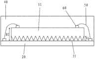
图2是根据本发明示例性实施例的芯片封装件的剖视图。如图2中所示,根据本发明示例性实施例的芯片封装件包括芯片11、基底20、粘附层31和包封层40。FIG. 2 is a cross-sectional view of a chip package according to an exemplary embodiment of the present invention. As shown in FIG. 2 , a chip package according to an exemplary embodiment of the present invention includes a
基底20可以是由诸如BT树脂(双马来酰亚胺三嗪树脂)等的各种绝缘材料以任意的形状形成的绝缘基板。基底20上可以形成有各种布线,以便于各种电路连接。The
芯片11可以通过粘附层31固定在基底20上。芯片11可以具有输入输出端60,输入输出端60可以通过引线50连接到基底20上,从而实现芯片11与基底20上的电路之间的电通信。The
粘附层31可以是晶片贴膜(DAF,Die attach film)或环氧树脂膜。The
包封层40可以形成在基底20的安装有芯片11的表面上,以包封芯片11、引线50和在基底20上的各种布线,从而保护它们不受外部环境影响。包封层20可以由诸如环氧树脂等的绝缘材料形成。The
如图2中所示,芯片11面向基底20的一侧表面(在下文中,称作下表面)为非平坦的。具体地讲,芯片11的下表面形成有凸起和凹陷图案,例如,锯齿状的凸起和凹进图案。芯片11的下表面的凸起和凹进图案由V型凸起和倒V型凹进交替排列而形成。此外,粘附层31的粘附材料填充在芯片11的下表面的倒V型凹进中,以将芯片11粘附并固定到基底20上。As shown in FIG. 2 , a side surface (hereinafter, referred to as a lower surface) of the
如果如图1中所示的结构,不在芯片11的下表面上形成V型的凸起和凹进图案,而将芯片11通过粘附层31粘附到基底20上,则芯片11和粘附层31的高度和为芯片11的高度H1与粘附层31的高度H2的和。然而,根据本发明的示例性实施例,由于在芯片11的下表面形成了V型的凸起和凹进图案,所以在形成粘附层31的粘附材料的固化过程中,粘附层31的粘附材料会填充在倒V型的凹进中。由于粘附层31本身一部分进入了芯片11的倒V型的凹进中,所以芯片11和粘附层31的高度和小于芯片11的高度H1与粘附层31的高度H2的和,因此,整体上减小了封装件的高度。如图2中所示,当粘附层31的材料恰好完全进入倒V型的凹进中时,芯片11和粘附层31的高度和只为芯片11的高度H1,大大地减小了芯片封装件的高度。If the structure shown in Figure 1 does not form V-shaped protrusions and concave patterns on the lower surface of the
此外,根据本示例性实施例,由于在芯片11的下表面形成有凸起和凹进图案,所以增大了芯片11和粘附层31的接触面积,从而可以增大芯片11的散热面积并提高芯片11的散热性能。In addition, according to the present exemplary embodiment, since the convex and concave patterns are formed on the lower surface of the
此外,由于在芯片11下表面形成有凸起和凹进图案,所以增大了芯片11和粘附层31的接触面积,从而提高芯片11与基底20的粘合强度。In addition, since the convex and concave patterns are formed on the lower surface of the
图3是根据本发明另一示例性实施例的芯片封装件的剖视图。FIG. 3 is a cross-sectional view of a chip package according to another exemplary embodiment of the present invention.
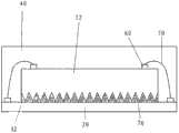
如图3中所示,根据本发明示例性实施例的芯片封装件包括芯片12、基底20、粘附层32和包封层40。除粘附层32中还包含散热颗粒70外,根据本示例性实施例的芯片封装件的结构与图2中示出的芯片封装件的结构基本相同。As shown in FIG. 3 , a chip package according to an exemplary embodiment of the present invention includes a
散热颗粒70可以是高导热性的金属颗粒,例如Ag颗粒。由于粘附层32中包含分散的散热颗粒70,所以可以大大地提高芯片12的散热性能。The
图4是根据本发明又一示例性实施例的芯片封装件的剖视图。FIG. 4 is a cross-sectional view of a chip package according to still another exemplary embodiment of the present invention.
如图4中所示,根据本发明示例性实施例的芯片封装件包括芯片13、基底20、粘附层33和包封层40。除在芯片13的下表面形成的凸起和凹进图案与图2中示出的芯片11的凸起和凹进图案不同之外,根据本示例性实施例的芯片封装件的结构与图2中示出的芯片封装件的结构基本相同。具体地讲,根据本示例性实施例,在芯片13的下表面形成的凸起和凹进图案可以为由交替排列的倒“ㄇ”型凸起和“ㄇ”型凹进形成的锯齿状的凸起和凹进图案。As shown in FIG. 4 , a chip package according to an exemplary embodiment of the present invention includes a
根据本示例性实施例的芯片封装件,由于芯片13的粘附到基底20的一侧表面形成“ㄇ”型的凸起和凹进图案,并且粘附层33的一部分材料填充在“ㄇ”型凹进中,所以如上所述,可以减小芯片封装件的整体高度并提高芯片的散热性能。According to the chip package of this exemplary embodiment, since the surface of one side of the
虽然图2和图4中分别示出了V型的凸起和凹进图案以及“ㄇ”型的凸起和凹进图案,但本领域技术人员应该认识到,本发明不限于上述形状的凸起和凹进图案,根据本发明的教导的各种形状的凸起和凹进图案都应在本发明的范围内。例如,根据本发明的凸起和凹进图案可以由柱状凸起、锥状凸起等构成。此外,这些凸起和凹进图案中的凸起图案和凹进图案可以均匀地分布以便于在芯片的表面上通过蚀刻来形成这些凸起和凹进图案。Although Fig. 2 and Fig. 4 show V-shaped protrusion and recess pattern and "ㄇ"-shaped protrusion and recess pattern respectively, those skilled in the art should realize that the present invention is not limited to the above-mentioned shapes of protrusions and recesses. Raised and recessed patterns, raised and recessed patterns of various shapes according to the teachings of the present invention are within the scope of the present invention. For example, the convex and concave patterns according to the present invention may be composed of columnar protrusions, tapered protrusions, and the like. In addition, the convex and concave patterns of the convex and concave patterns may be uniformly distributed so as to form the convex and concave patterns by etching on the surface of the chip.
图5a至图5d是根据本发明示例性实施例的芯片封装件的制造方法的剖视图。下面将参照图5a至图5d来详细地描述根据本发明示例性实施例的芯片封装件的制造方法。5a to 5d are cross-sectional views of a method of manufacturing a chip package according to an exemplary embodiment of the present invention. A method of manufacturing a chip package according to an exemplary embodiment of the present invention will be described in detail below with reference to FIGS. 5 a to 5 d.
如图5a所示,首先可以准备芯片11。将芯片11的将粘附到基底上的一侧表面(即,下表面)形成有凸起和凹进图案,如图5a中所示,该凸起和凹进图案为锯齿状,即,由V型凸起和倒V凹进交替排列的凸起和凹进图案。这里,可以通过各向异性蚀刻来形成如图5a中所示的凸起和凹进图案,但本发明不限于此。此外,芯片11的与所述下表面相对的另一侧表面(即,上表面)可以形成输入输出端60。As shown in Fig. 5a, first the
如图5b中所示,将粘附材料31’设置在基底20上。粘附材料31’可以为晶片贴膜或环氧树脂。这里使用的粘附材料31’中可以包含散热颗粒,散热颗粒可以为高导热性的金属颗粒,例如Ag颗粒。An adhesive material 31' is disposed on the
然后,将芯片11放置在基底20上,使芯片11的具有凸起和凹进图案的下表面位于粘附材料31’上。Then, the
接下来,如图5c中所示,进行固化,使得部分粘附材料31’填充在芯片的凹进表面中。这里可以使用热固化处理粘附材料30’,并且在芯片11的自重不足的情况下,可以在芯片11上施加适当的压力以使芯片11的凸起进入粘附材料31’中。Next, as shown in Fig. 5c, curing is performed so that part of the adhesive material 31' is filled in the recessed surface of the chip. Here, thermal curing can be used to process the adhesive material 30', and when the self-weight of the
最后,如图5d中所示,用诸如环氧树脂等的包封材料对芯片11等进行包封,从而形成芯片封装件。在进行包封之前,可以通过引线50将输入输出端60与基底20进行连接,从而实现芯片11与基底20之间的电通信。Finally, as shown in FIG. 5 d , the
通过以上对根据本发明示例性实施例的芯片封装件及其制造方法的描述中可以看出,由于在芯片的与基底结合的一侧表面上形成凸起和凹进图案,所以通过粘附层将芯片粘附到基底的情况下,粘附材料可以填充在凹进图案中而减小粘附层的高度,从而实现芯片封装件的小型化。此外,由于粘附材料填充在凹进图案中,所以可以增大芯片和粘附材料之间的接触面,因此可以提高芯片的散热效果。As can be seen from the above description of the chip package and its manufacturing method according to the exemplary embodiment of the present invention, since the convex and concave patterns are formed on the surface of the chip on the side bonded to the substrate, the adhesive layer In the case of attaching a chip to a substrate, the adhesive material may be filled in the recessed pattern to reduce the height of the adhesive layer, thereby achieving miniaturization of the chip package. In addition, since the adhesive material is filled in the concave pattern, the contact surface between the chip and the adhesive material can be increased, and thus the heat dissipation effect of the chip can be improved.
尽管已经参照本发明的示例性实施例示出并描述了本发明,但是本发明的范围不限于此。在不脱离本发明的精神或教导的情况,可以在形式和细节上对本发明做出各种修改。本发明的范围由权利要求及其等同物限定。While the invention has been shown and described with reference to the exemplary embodiments of the invention, the scope of the invention is not limited thereto. Various modifications in form and detail may be made to the present invention without departing from the spirit or teachings of the present invention. The scope of the invention is defined by the claims and their equivalents.
Claims (12)
Priority Applications (1)
| Application Number | Priority Date | Filing Date | Title |
|---|---|---|---|
| CN2012100251617ACN102543910A (en) | 2012-02-06 | 2012-02-06 | Chip packaging component and manufacturing method thereof |
Applications Claiming Priority (1)
| Application Number | Priority Date | Filing Date | Title |
|---|---|---|---|
| CN2012100251617ACN102543910A (en) | 2012-02-06 | 2012-02-06 | Chip packaging component and manufacturing method thereof |
Publications (1)
| Publication Number | Publication Date |
|---|---|
| CN102543910Atrue CN102543910A (en) | 2012-07-04 |
Family
ID=46350439
Family Applications (1)
| Application Number | Title | Priority Date | Filing Date |
|---|---|---|---|
| CN2012100251617APendingCN102543910A (en) | 2012-02-06 | 2012-02-06 | Chip packaging component and manufacturing method thereof |
Country Status (1)
| Country | Link |
|---|---|
| CN (1) | CN102543910A (en) |
Cited By (3)
| Publication number | Priority date | Publication date | Assignee | Title |
|---|---|---|---|---|
| JP2019024121A (en)* | 2015-07-01 | 2019-02-14 | 三菱電機株式会社 | Semiconductor device and method of manufacturing semiconductor device |
| CN112103259A (en)* | 2020-09-28 | 2020-12-18 | 东莞记忆存储科技有限公司 | Chip packaging structure with graphene heat dissipation coating and preparation method thereof |
| WO2023206122A1 (en)* | 2022-04-27 | 2023-11-02 | 重庆康佳光电技术研究院有限公司 | Chip assembly and preparation method therefor, and preparation method for display panel |
Citations (10)
| Publication number | Priority date | Publication date | Assignee | Title |
|---|---|---|---|---|
| JPH03237733A (en)* | 1989-11-16 | 1991-10-23 | Mitsubishi Electric Corp | Ic |
| JPH05308083A (en)* | 1992-04-30 | 1993-11-19 | Nippon Steel Corp | Semiconductor device |
| JPH06196511A (en)* | 1992-12-24 | 1994-07-15 | Kawasaki Steel Corp | Semiconductor device |
| US5545589A (en)* | 1993-01-28 | 1996-08-13 | Matsushita Electric Industrial Co., Ltd. | Method of forming a bump having a rugged side, a semiconductor device having the bump, and a method of mounting a semiconductor unit and a semiconductor device |
| US20020003293A1 (en)* | 2000-07-04 | 2002-01-10 | Yutaka Kobayashi | Semiconductor device and method for fabricating same |
| CN1357916A (en)* | 2000-12-14 | 2002-07-10 | 胜开科技股份有限公司 | Integrated circuit packaging structure and manufacturing method thereof |
| CN1574300A (en)* | 2003-05-22 | 2005-02-02 | 新光电气工业株式会社 | Packaging component and semiconductor package |
| US20060223231A1 (en)* | 2005-04-05 | 2006-10-05 | Oki Electric Industry Co., Ltd. | Packing method for electronic components |
| CN101164165A (en)* | 2005-04-26 | 2008-04-16 | 大日本印刷株式会社 | Circuit member, circuit member manufacturing method, semiconductor device and multilayer structure on circuit member surface |
| US20090267104A1 (en)* | 2008-04-28 | 2009-10-29 | Lighthouse Technology Co., Ltd | Light-emitting diode package |
- 2012
- 2012-02-06CNCN2012100251617Apatent/CN102543910A/enactivePending
Patent Citations (10)
| Publication number | Priority date | Publication date | Assignee | Title |
|---|---|---|---|---|
| JPH03237733A (en)* | 1989-11-16 | 1991-10-23 | Mitsubishi Electric Corp | Ic |
| JPH05308083A (en)* | 1992-04-30 | 1993-11-19 | Nippon Steel Corp | Semiconductor device |
| JPH06196511A (en)* | 1992-12-24 | 1994-07-15 | Kawasaki Steel Corp | Semiconductor device |
| US5545589A (en)* | 1993-01-28 | 1996-08-13 | Matsushita Electric Industrial Co., Ltd. | Method of forming a bump having a rugged side, a semiconductor device having the bump, and a method of mounting a semiconductor unit and a semiconductor device |
| US20020003293A1 (en)* | 2000-07-04 | 2002-01-10 | Yutaka Kobayashi | Semiconductor device and method for fabricating same |
| CN1357916A (en)* | 2000-12-14 | 2002-07-10 | 胜开科技股份有限公司 | Integrated circuit packaging structure and manufacturing method thereof |
| CN1574300A (en)* | 2003-05-22 | 2005-02-02 | 新光电气工业株式会社 | Packaging component and semiconductor package |
| US20060223231A1 (en)* | 2005-04-05 | 2006-10-05 | Oki Electric Industry Co., Ltd. | Packing method for electronic components |
| CN101164165A (en)* | 2005-04-26 | 2008-04-16 | 大日本印刷株式会社 | Circuit member, circuit member manufacturing method, semiconductor device and multilayer structure on circuit member surface |
| US20090267104A1 (en)* | 2008-04-28 | 2009-10-29 | Lighthouse Technology Co., Ltd | Light-emitting diode package |
Cited By (3)
| Publication number | Priority date | Publication date | Assignee | Title |
|---|---|---|---|---|
| JP2019024121A (en)* | 2015-07-01 | 2019-02-14 | 三菱電機株式会社 | Semiconductor device and method of manufacturing semiconductor device |
| CN112103259A (en)* | 2020-09-28 | 2020-12-18 | 东莞记忆存储科技有限公司 | Chip packaging structure with graphene heat dissipation coating and preparation method thereof |
| WO2023206122A1 (en)* | 2022-04-27 | 2023-11-02 | 重庆康佳光电技术研究院有限公司 | Chip assembly and preparation method therefor, and preparation method for display panel |
Similar Documents
| Publication | Publication Date | Title |
|---|---|---|
| CN101221946B (en) | Semiconductor package and method for manufacturing system-in-package module | |
| TWI415228B (en) | Semiconductor package structure, flip chip package, and method for forming semiconductor flip chip package | |
| CN102569214B (en) | Three-dimensional system-in-package stacked package structure | |
| CN102738094B (en) | Semiconductor packaging structure for stacking and manufacturing method thereof | |
| TWI495021B (en) | Chip package structure and method for manufacturing the same | |
| US20080093733A1 (en) | Chip package and manufacturing method thereof | |
| CN107305883A (en) | Electronic package and manufacturing method thereof | |
| CN106169449A (en) | Thin film flip chip package and heat dissipation method thereof | |
| US7564123B1 (en) | Semiconductor package with fastened leads | |
| CN100378972C (en) | Heat sink and package using the same | |
| TWI778560B (en) | Package structure and manufacturing method thereof | |
| TW571406B (en) | High performance thermally enhanced package and method of fabricating the same | |
| CN102543910A (en) | Chip packaging component and manufacturing method thereof | |
| CN107591378A (en) | Heat dissipation type packaging structure | |
| CN101944520B (en) | Semiconductor packaging structure and semiconductor packaging process | |
| TWI536515B (en) | Semiconductor package device with a heat dissipation structure and the packaging method thereof | |
| TWI388041B (en) | Semiconductor package having heat-dissipating structure | |
| CN101241902A (en) | Multi-chip semiconductor package and manufacturing method thereof | |
| TWI425676B (en) | Structure of the semiconductir package | |
| US6696750B1 (en) | Semiconductor package with heat dissipating structure | |
| EP2545584B1 (en) | Package having spaced apart heat sink | |
| CN101556940B (en) | Semiconductor package structure with heat sink | |
| CN106971981A (en) | Semiconductor package, semiconductor device and method of manufacturing semiconductor package | |
| TW201836114A (en) | Substrate-less package structure | |
| CN109935557B (en) | Electronic package and its manufacturing method |
Legal Events
| Date | Code | Title | Description |
|---|---|---|---|
| C06 | Publication | ||
| PB01 | Publication | ||
| C10 | Entry into substantive examination | ||
| SE01 | Entry into force of request for substantive examination | ||
| C12 | Rejection of a patent application after its publication | ||
| RJ01 | Rejection of invention patent application after publication | Application publication date:20120704 |