CN102543865A - Semiconductor device - Google Patents
Semiconductor deviceDownload PDFInfo
- Publication number
- CN102543865A CN102543865ACN2012100467749ACN201210046774ACN102543865ACN 102543865 ACN102543865 ACN 102543865ACN 2012100467749 ACN2012100467749 ACN 2012100467749ACN 201210046774 ACN201210046774 ACN 201210046774ACN 102543865 ACN102543865 ACN 102543865A
- Authority
- CN
- China
- Prior art keywords
- layer
- semiconductor
- transistor
- conductive layer
- semiconductor layer
- Prior art date
- Legal status (The legal status is an assumption and is not a legal conclusion. Google has not performed a legal analysis and makes no representation as to the accuracy of the status listed.)
- Granted
Links
Images


Classifications
- H—ELECTRICITY
- H10—SEMICONDUCTOR DEVICES; ELECTRIC SOLID-STATE DEVICES NOT OTHERWISE PROVIDED FOR
- H10D—INORGANIC ELECTRIC SEMICONDUCTOR DEVICES
- H10D86/00—Integrated devices formed in or on insulating or conducting substrates, e.g. formed in silicon-on-insulator [SOI] substrates or on stainless steel or glass substrates
- H10D86/01—Manufacture or treatment
- H10D86/021—Manufacture or treatment of multiple TFTs
- H10D86/0214—Manufacture or treatment of multiple TFTs using temporary substrates
- H—ELECTRICITY
- H10—SEMICONDUCTOR DEVICES; ELECTRIC SOLID-STATE DEVICES NOT OTHERWISE PROVIDED FOR
- H10D—INORGANIC ELECTRIC SEMICONDUCTOR DEVICES
- H10D86/00—Integrated devices formed in or on insulating or conducting substrates, e.g. formed in silicon-on-insulator [SOI] substrates or on stainless steel or glass substrates
- H10D86/01—Manufacture or treatment
- H10D86/021—Manufacture or treatment of multiple TFTs
- H10D86/0241—Manufacture or treatment of multiple TFTs using liquid deposition, e.g. printing
- H—ELECTRICITY
- H10—SEMICONDUCTOR DEVICES; ELECTRIC SOLID-STATE DEVICES NOT OTHERWISE PROVIDED FOR
- H10D—INORGANIC ELECTRIC SEMICONDUCTOR DEVICES
- H10D86/00—Integrated devices formed in or on insulating or conducting substrates, e.g. formed in silicon-on-insulator [SOI] substrates or on stainless steel or glass substrates
- H10D86/40—Integrated devices formed in or on insulating or conducting substrates, e.g. formed in silicon-on-insulator [SOI] substrates or on stainless steel or glass substrates characterised by multiple TFTs
- H10D86/471—Integrated devices formed in or on insulating or conducting substrates, e.g. formed in silicon-on-insulator [SOI] substrates or on stainless steel or glass substrates characterised by multiple TFTs having different architectures, e.g. having both top-gate and bottom-gate TFTs
- H—ELECTRICITY
- H10—SEMICONDUCTOR DEVICES; ELECTRIC SOLID-STATE DEVICES NOT OTHERWISE PROVIDED FOR
- H10D—INORGANIC ELECTRIC SEMICONDUCTOR DEVICES
- H10D86/00—Integrated devices formed in or on insulating or conducting substrates, e.g. formed in silicon-on-insulator [SOI] substrates or on stainless steel or glass substrates
- H10D86/40—Integrated devices formed in or on insulating or conducting substrates, e.g. formed in silicon-on-insulator [SOI] substrates or on stainless steel or glass substrates characterised by multiple TFTs
- H10D86/60—Integrated devices formed in or on insulating or conducting substrates, e.g. formed in silicon-on-insulator [SOI] substrates or on stainless steel or glass substrates characterised by multiple TFTs wherein the TFTs are in active matrices
Landscapes
- Thin Film Transistor (AREA)
- Electroluminescent Light Sources (AREA)
- Liquid Crystal (AREA)
- Metal-Oxide And Bipolar Metal-Oxide Semiconductor Integrated Circuits (AREA)
- Devices For Indicating Variable Information By Combining Individual Elements (AREA)
- Dram (AREA)
- Shift Register Type Memory (AREA)
Abstract
Description
Translated fromChinese本发明专利申请是申请日为2008年6月30日、申请号为200810129391.1、名称为“半导体装置”的发明专利申请的分案申请。The patent application of the present invention is a divisional application of the patent application for invention with the filing date of June 30, 2008, the application number of 200810129391.1, and the title of "semiconductor device".
技术领域technical field
本发明涉及物体、方法,或者制作物体的方法。特别涉及显示装置或者半导体装置。尤其涉及将单晶复制到玻璃基板而形成的显示装置或者半导体装置。The present invention relates to objects, methods, or methods of making objects. In particular, it relates to a display device or a semiconductor device. In particular, it relates to a display device or a semiconductor device formed by replicating a single crystal onto a glass substrate.
背景技术Background technique
近年来,液晶显示装置、场致发光(EL)显示装置等的平板显示器备受瞩目。In recent years, flat panel displays such as liquid crystal display devices and electroluminescent (EL) display devices have attracted attention.
作为平板显示器的驱动方式,包括无源矩阵方式及有源矩阵方式。有源矩阵方式与无源矩阵方式相比,具有下述优点:能够实现低功耗化、高清晰度、基板的大型化等。The driving method of the flat panel display includes a passive matrix method and an active matrix method. Compared with the passive matrix method, the active matrix method has advantages such as lower power consumption, higher definition, and larger substrate size.
在将驱动电路设置于面板的外部的结构中,由于可以采用使用了单晶硅的IC作为驱动电路,所以不会发生由于驱动电路的速度所引起的问题。然而,在这样设置IC的情况下,由于需要分别准备面板与IC,还需要进行面板与IC的连接工序等,因此不能充分地降低制造成本。In the structure in which the driving circuit is provided outside the panel, since an IC using single crystal silicon can be used as the driving circuit, problems due to the speed of the driving circuit do not occur. However, in the case of installing the ICs in this way, it is necessary to prepare the panel and the ICs separately, and also to perform a connection process between the panel and the ICs, etc., so that the manufacturing cost cannot be sufficiently reduced.
因此,从降低制造成本的角度,采用了将像素部与驱动电路部形成为一体的方法(例如,参照专利文献1)。Therefore, from the viewpoint of reducing the manufacturing cost, a method of integrating the pixel portion and the driver circuit portion has been adopted (for example, refer to Patent Document 1).
专利文献1日本专利特开平8-6053号公报
在专利文献1所示的情况中,作为驱动电路的半导体层,与像素部同样的,使用非晶硅或微晶硅、以及多晶硅等的非单晶硅。然而,非晶硅就不用说了、即使在使用微晶硅与多晶硅的情况下,都存在其特性远远不及使用单晶硅的情况的问题。尤其,在现有的驱动电路一体型的面板所使用的半导体层中,由于得不到必要且充分的迁移率,在面临制造驱动电路这种要求高速操作的半导体装置时成为很严重的问题。In the case disclosed in
发明内容Contents of the invention
鉴于上述问题,本发明的目的在于提供降低了制造成本的半导体装置。或者,其目的在于提供设置有可以高速操作的电路的半导体装置。或者,其目的在于提供低功耗的半导体装置。In view of the above problems, an object of the present invention is to provide a semiconductor device with reduced manufacturing cost. Alternatively, the object is to provide a semiconductor device provided with a circuit that can operate at high speed. Alternatively, the object is to provide a semiconductor device with low power consumption.
在本发明中,将硅层从单晶基板分离(剥离),并将其粘贴(复制)到玻璃基板上。或者,将单晶基板粘贴在玻璃基板上,并通过将单晶基板分离,从而在玻璃基板上形成硅层。并且,将硅层加工成岛形。之后,再次将硅层从单晶基板分离,并将其粘贴在玻璃基板上。或者,将单晶基板粘贴在玻璃基板上,并通过将单晶基板分离,从而在玻璃基板上形成硅层。并且,再次将硅层加工成岛形。In the present invention, the silicon layer is separated (peeled) from the single crystal substrate, and pasted (replicated) on the glass substrate. Alternatively, a single crystal substrate is attached to a glass substrate, and the single crystal substrate is separated to form a silicon layer on the glass substrate. And, the silicon layer is processed into an island shape. After that, the silicon layer is separated from the single crystal substrate again and pasted on the glass substrate. Alternatively, a single crystal substrate is attached to a glass substrate, and the single crystal substrate is separated to form a silicon layer on the glass substrate. And, the silicon layer is processed into an island shape again.
因此,使用这些硅层在玻璃基板上形成TFT。Therefore, TFTs are formed on glass substrates using these silicon layers.
此时,同时形成使用有非晶硅或微晶硅的TFT。At this time, TFTs using amorphous silicon or microcrystalline silicon are formed at the same time.
并且,在这些TFT中,共有作为栅电极其作用的导电层或作为源电极、漏电极起作用的导电层,并同时形成膜。通过这样,能够减少制造步骤。Furthermore, in these TFTs, a conductive layer functioning as a gate electrode or a conductive layer functioning as a source electrode and a drain electrode are shared, and films are formed at the same time. By doing so, the number of manufacturing steps can be reduced.
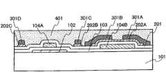
本发明的特征在于,在绝缘基板上方具有第一半导体层;在第一半导体层上方具有第一绝缘层;在第一绝缘层上方具有第一和第二导电层;在第一和第二导电层上方具有第二绝缘层;在第二绝缘层上方具有第二半导体层;在第二半导体层上方具有第三导电层;在第二绝缘层上方具有第四导电层;在第三和第四导电层上方具有第三绝缘层;在第三绝缘层上方具有第五导电层,其中,第一半导体层具有作为第一晶体管的激活层的功能,第二半导体层具有作为第二晶体管的激活层的功能,而且第一半导体层和第二半导体层具有不同的特性。The present invention is characterized in that there is a first semiconductor layer above the insulating substrate; there is a first insulating layer above the first semiconductor layer; there are first and second conductive layers above the first insulating layer; a second insulating layer over the layer; a second semiconducting layer over the second insulating layer; a third conducting layer over the second semiconducting layer; a fourth conducting layer over the second insulating layer; There is a third insulating layer above the conductive layer; a fifth conductive layer is arranged above the third insulating layer, wherein the first semiconductor layer has a function as an active layer of the first transistor, and the second semiconductor layer has a function as an active layer of the second transistor. function, and the first semiconductor layer and the second semiconductor layer have different characteristics.
本发明的特征在于,在上述结构中,第一绝缘层具有作为所述第一晶体管的栅极绝缘层的功能,第一导电层具有第一晶体管的栅电极的功能。The present invention is characterized in that, in the above structure, the first insulating layer functions as a gate insulating layer of the first transistor, and the first conductive layer functions as a gate electrode of the first transistor.
本发明的特征在于,在上述结构中,第二绝缘层具有作为第二晶体管的栅极绝缘层的功能,第二导电层具有作为第二晶体管的栅电极的功能。The present invention is characterized in that, in the above structure, the second insulating layer functions as a gate insulating layer of the second transistor, and the second conductive layer functions as a gate electrode of the second transistor.
本发明的特征在于,在上述结构中,第五导电层通过设置于第三绝缘层的接触孔,与第四导电层电连接。The present invention is characterized in that, in the above structure, the fifth conductive layer is electrically connected to the fourth conductive layer through a contact hole provided in the third insulating layer.
本发明的特征在于,在上述结构中,第五导电层通过设置于第一绝缘层、第二绝缘层及第三绝缘层的接触孔,与第一半导体层电连接。The present invention is characterized in that, in the above structure, the fifth conductive layer is electrically connected to the first semiconductor layer through contact holes provided in the first insulating layer, the second insulating layer, and the third insulating layer.
本发明的特征在于,在上述结构中,第三导电层与第二半导体层电连接。The present invention is characterized in that, in the above structure, the third conductive layer is electrically connected to the second semiconductor layer.
本发明的特征在于,在上述结构中,第一半导体层具有结晶性。The present invention is characterized in that, in the above structure, the first semiconductor layer has crystallinity.
本发明的特征在于,在上述结构中,第二半导体层具有非晶半导体。The present invention is characterized in that, in the above structure, the second semiconductor layer has an amorphous semiconductor.
本发明的特征在于,在上述结构中,第二半导体层具有微晶半导体。The present invention is characterized in that, in the above structure, the second semiconductor layer has a microcrystalline semiconductor.
另外,在本说明书中,可以使用各种方式的开关,例如有电子开关或机械开关等。换而言之,只要它可以控制电流的流动就可以,而不限定于特定开关。例如,作为开关,可以使用晶体管(例如,双极晶体管或MOS晶体管等)、二极管(例如,PN二极管、PIN二极管、肖特基二极管、MIM(Metal Insulator Metal;金属-绝缘体-金属)二极管、MIS(Metal InsulatorSemiconductor;金属-绝缘体-半导体)二极管、二极管连接的晶体管等)、或可控硅整流器等。或者,可以使用组合它们后的逻辑电路作为开关。In addition, in this specification, various types of switches may be used, for example, electronic switches, mechanical switches, and the like. In other words, as long as it can control the flow of current, it is not limited to a specific switch. For example, as switches, transistors (for example, bipolar transistors or MOS transistors, etc.), diodes (for example, PN diodes, PIN diodes, Schottky diodes, MIM (Metal Insulator Metal; metal-insulator-metal) diodes, MIS (Metal InsulatorSemiconductor; metal-insulator-semiconductor) diodes, diode-connected transistors, etc.), or silicon controlled rectifiers, etc. Alternatively, a logic circuit combining them may be used as a switch.
作为机械开关的例子,有像数字微镜装置(DMD)那样,利用MEMS(微电子机械系统)技术的开关。该开关具有以机械方式可动的电极,并且通过该电极移动来控制连接和不连接以实现工作。As an example of a mechanical switch, there is a switch utilizing MEMS (Micro Electro Mechanical System) technology, such as a digital micromirror device (DMD). The switch has electrodes that are mechanically movable, and the connection and disconnection are controlled by the movement of the electrodes to achieve operation.
在使用晶体管以作为开关的情况下,由于该晶体管作为简单的开关来工作,因此对晶体管的极性(导电类型)没有特别限制。然而,在想要抑制截止电流的情况下,优选采用具有较小截止电流的极性的晶体管。作为截止电流较小的晶体管,有具有LDD区的晶体管或具有多栅极结构的晶体管等。或者,当在作为开关来工作的晶体管的源极端子的电位接近于低电位侧电源(Vss、GND、0V等)的电位的状态下使其工作时,优选采用N沟道型晶体管。相反,当在源极端子的电位接近于高电位侧电源(Vdd等)的电位的状态下使其工作时,优选采用P沟道型晶体管。这是因为如下缘故:若是N沟道型晶体管,则当在源极端子接近于低电位侧电源的电位的状态下使其工作时,若是P沟道型晶体管,则当在源极端子接近于高电位侧电源的电位的状态下使其工作时,可以增大栅极-源极间电压的绝对值,因此作为开关使其更精确地工作。另外,这是因为进行源极跟随工作的情况较少,所以导致输出电压变小的情况少。In the case of using a transistor as a switch, since the transistor operates as a simple switch, there is no particular limitation on the polarity (conduction type) of the transistor. However, in the case where it is desired to suppress the off-current, it is preferable to employ a transistor having a polarity with a smaller off-current. As transistors having a small off-state current, there are transistors having an LDD region, transistors having a multi-gate structure, and the like. Alternatively, when a transistor operating as a switch is operated with the potential of its source terminal close to the potential of a low-potential side power supply (Vss, GND, 0V, etc.), an N-channel transistor is preferably used. Conversely, when the source terminal is operated in a state where the potential of the source terminal is close to the potential of the high-potential side power supply (Vdd, etc.), it is preferable to use a P-channel transistor. This is because of the following reason: if it is an N-channel type transistor, when it is operated in a state where the source terminal is close to the potential of the low-potential side power supply, if it is a P-channel type transistor, when the source terminal is close to the potential of the low-potential power supply When operating at the potential state of the high-potential side power supply, the absolute value of the gate-source voltage can be increased, so it can be operated more precisely as a switch. In addition, this is because the source follower operation is rarely performed, so the output voltage is rarely reduced.
另外,可以通过使用N沟道型晶体管和P沟道型晶体管两者来形成CMOS型开关以作为开关。当采用CMOS型开关时,因为若P沟道型晶体管或N沟道型晶体管中的某一方的晶体管导通则电流流动,因此作为开关更容易起作用。例如,无论输入开关的输入信号的电压是高或低,都可以适当地输出电压。而且,由于可以降低用于使开关导通或截止的信号的电压振幅值,所以还可以减少耗电量。In addition, a CMOS type switch may be formed by using both an N-channel type transistor and a P-channel type transistor as a switch. When a CMOS switch is used, current flows when either the P-channel transistor or the N-channel transistor is turned on, and thus functions as a switch more easily. For example, regardless of whether the voltage of the input signal input to the switch is high or low, the voltage can be appropriately output. Furthermore, since the voltage amplitude value of the signal for turning on or off the switch can be reduced, power consumption can also be reduced.
另外,在将晶体管作为开关来使用的情况下,开关具有输入端子(源极端子或漏极端子的一方)、输出端子(源极端子或漏极端子的另一方)、以及控制导通的端子(栅极端子)。另一方面,在将二极管作为开关来使用的情况下,开关有时不具有控制导通的端子。因此,与使用晶体管作为开关的情况相比,通过使用二极管作为开关的情况可以减少用于控制端子的布线。In addition, when a transistor is used as a switch, the switch has an input terminal (one of a source terminal or a drain terminal), an output terminal (the other of a source terminal or a drain terminal), and a terminal for controlling conduction. (gate terminal). On the other hand, when a diode is used as a switch, the switch may not have a terminal for controlling conduction. Therefore, the wiring for the control terminal can be reduced by the case of using the diode as the switch compared to the case of using the transistor as the switch.
另外,在本说明书中,明确地记载“A和B连接”的情况包括如下情况:A和B电连接的情况;A和B以功能方式连接的情况;以及A和B直接连接的情况。在此,A和B为对象物(例如,装置、元件、电路、布线、电极、端子、导电膜、层等)。因此,规定的连接关系还包括附图或文章所示的连接关系以外的连接关系,而不局限于如附图或文章所示的连接关系。In addition, in this specification, the case where "A and B are connected" explicitly includes the following cases: the case where A and B are electrically connected; the case where A and B are functionally connected; and the case where A and B are directly connected. Here, A and B are objects (for example, devices, elements, circuits, wiring, electrodes, terminals, conductive films, layers, etc.). Therefore, the specified connection relationship also includes the connection relationship other than the connection relationship shown in the drawings or articles, and is not limited to the connection relationship shown in the drawings or articles.
例如,在A和B电连接的情况下,也可以在A和B之间配置一个以上的能够电连接A和B的元件(例如开关、晶体管、电容元件、电感器、电阻元件、二极管等)。或者,在A和B以功能方式连接的情况下,也可以在A和B之间配置一个以上的能够以功能方式连接A和B的电路(例如,逻辑电路(反相器、NAND电路、NOR电路等)、信号转换电路(DA转换电路、AD转换电路、γ校正电路等)、电位电平转换电路(电源电路(升压电路、降压电路等)、改变信号的电位电平的电平转移电路等)、电压源、电流源、切换电路、放大电路(能够增大信号振幅或电流量等的电路、运算放大器、差动放大电路、源极跟随电路、缓冲电路等)、信号产生电路、存储电路、控制电路等)。或者,在A和B直接连接的情况下,也可以直接连接A和B且在其中间不夹有其它元件或其它电路。For example, when A and B are electrically connected, one or more elements capable of electrically connecting A and B (such as switches, transistors, capacitive elements, inductors, resistive elements, diodes, etc.) may be arranged between A and B. . Alternatively, in the case where A and B are functionally connected, more than one circuit capable of functionally connecting A and B (for example, a logic circuit (inverter, NAND circuit, NOR circuit, etc.) circuit, etc.), signal conversion circuit (DA conversion circuit, AD conversion circuit, γ correction circuit, etc.), potential level conversion circuit (power supply circuit (boost circuit, step-down circuit, etc.), level for changing the potential level of the signal Transfer circuits, etc.), voltage sources, current sources, switching circuits, amplifier circuits (circuits capable of increasing signal amplitude or current, operational amplifiers, differential amplifier circuits, source follower circuits, buffer circuits, etc.), signal generation circuits , storage circuits, control circuits, etc.). Alternatively, in the case where A and B are directly connected, A and B may also be directly connected without interposing other elements or other circuits therebetween.
另外,当明确地记载“A和B直接连接”的情况,包括如下情况:A和B直接连接(即,A和B连接且在其中间不夹有其它元件或其它电路)的情况;以及A和B电连接(即,A和B连接且在其中间夹有其它元件或其它电路)的情况。In addition, when it is clearly stated that "A and B are directly connected", the following cases are included: A and B are directly connected (that is, A and B are connected without interposing other elements or other circuits); and A A case where it is electrically connected to B (that is, A and B are connected with other elements or other circuits interposed therebetween).
另外,当明确地记载“A和B电连接”的情况,包括如下情况:A和B电连接(即,A和B连接且在其中间夹有其它元件或其它电路)的情况;A和B以功能方式连接(即,A和B以功能方式连接且在其中间夹有其它电路)的情况;以及,A和B直接连接(即,A和B连接且其中间不夹有其它元件或其它电路)的情况。总之,明确地记载“电连接”的情况与只是简单地记载“连接”的情况相同。In addition, when it is clearly stated that "A and B are electrically connected", it includes the following situations: A and B are electrically connected (that is, A and B are connected with other components or other circuits interposed therebetween); A and B The case where A and B are functionally connected (that is, A and B are functionally connected with other circuits interposed therebetween); and A and B are directly connected (that is, A and B are connected without interposing other components or other circuit). In short, the case where "electrically connected" is explicitly described is the same as the case where "connection" is simply described.
另外,本发明的显示元件、作为具有显示元件的装置的显示装置、发光元件、以及作为具有发光元件的装置的发光装置,可以采用各种方式或各种元件。例如,作为显示元件、显示装置、发光元件或发光装置,可以使用利用电磁作用来改变对比度、亮度、反射率、透过率等的显示介质,如EL元件(包含有机物及无机物的EL元件、有机EL元件、无机EL元件)、电子发射元件、液晶元件、电子墨水、电泳元件、光栅阀(GLV)、等离子体显示器(PDP)、数字微镜装置(DMD)、压电陶瓷显示器、碳纳米管等。此外,作为使用了EL元件的显示装置,可以举出EL显示器,作为使用了电子发射元件的显示装置,可以举出场致发光显示器(FED)或SED方式平面型显示器(SED:Surface-conduction Electron-emitter Display;表面传导电子发射显示器)等,作为使用了液晶元件的显示装置,可以举出液晶显示器(透过型液晶显示器、半透过型液晶显示器、反射型液晶显示器、直观型液晶显示器、投射型液晶显示器),并且作为使用了电子墨水或电泳元件的显示装置,可以举出电子纸。In addition, the display device of the present invention, the display device which is a device having a display device, the light emitting device, and the light emitting device which is a device having a light emitting device can employ various forms or various devices. For example, as a display element, a display device, a light-emitting element or a light-emitting device, it is possible to use a display medium that uses electromagnetic action to change contrast, brightness, reflectivity, transmittance, etc., such as EL elements (including organic and inorganic EL elements, Organic EL element, inorganic EL element), electron emission element, liquid crystal element, electronic ink, electrophoretic element, grating valve (GLV), plasma display (PDP), digital micromirror device (DMD), piezoelectric ceramic display, carbon nano tube etc. In addition, as a display device using an EL element, an EL display can be mentioned, and as a display device using an electron emission element, an electroluminescence display (FED) or an SED flat display (SED: Surface-conduction Electron- emitter Display; surface conduction electron emission display), etc., as a display device using a liquid crystal element, a liquid crystal display (transmissive liquid crystal display, semi-transmissive liquid crystal display, reflective liquid crystal display, direct-view liquid crystal display, projection type liquid crystal display), and as a display device using electronic ink or an electrophoretic element, electronic paper can be cited.
另外,EL元件是具有阳极、阴极、以及夹在阳极和阴极之间的EL层的元件。另外,作为EL层,可以使用利用来自单重态激子的发光(荧光)的层、利用来自三重态激子的发光(磷光)的层、包括利用来自单重态激子的发光(荧光)和利用来自三重态激子的发光(磷光)的层、利用有机物形成的层、利用无机物形成的层、包括利用有机物形成和利用无机物形成的层、高分子材料、低分子材料、以及包含高分子材料和低分子材料的层等。然而,不限定于此,可以使用各种元件作为EL元件。In addition, the EL element is an element having an anode, a cathode, and an EL layer sandwiched between the anode and the cathode. In addition, as the EL layer, a layer that utilizes light emission (fluorescence) from singlet excitons, a layer that utilizes light emission (phosphorescence) from triplet excitons, and a layer that utilizes light emission (fluorescence) from singlet excitons and a layer utilizing light emission (phosphorescence) from triplet excitons, a layer formed using an organic substance, a layer formed using an inorganic substance, including a layer formed using an organic substance and a layer formed using an inorganic substance, a high molecular material, a low molecular material, and a layer including A layer of high molecular material and low molecular material, etc. However, it is not limited thereto, and various elements can be used as the EL element.
另外,电子发射元件是将高电场集中到尖锐的阴极并抽出电子的元件。例如,作为电子发射元件,可以使用主轴(spindle)型、碳纳米管(CNT)型、层叠有金属-绝缘体-金属的MIM(Metal-Insulator-Metal)型、层叠有金属-绝缘体-半导体的MIS(Metal-Insulator-Semiconductor)型、MOS型、硅型、薄膜二极管型、金刚石型、表面传导发射SCD型等。然而,不限定于此,可以使用各种元件作为电子发射元件。In addition, the electron emission element is an element that concentrates a high electric field to a sharp cathode and extracts electrons. For example, as an electron emission element, a spindle type, a carbon nanotube (CNT) type, a metal-insulator-metal stacked MIM (Metal-Insulator-Metal) type, and a metal-insulator-semiconductor stacked MIS can be used. (Metal-Insulator-Semiconductor) type, MOS type, silicon type, thin film diode type, diamond type, surface conduction emission SCD type, etc. However, it is not limited thereto, and various elements can be used as the electron emission element.
另外,液晶元件是利用液晶的光学调制作用来控制光的透过或非透过的元件,是利用一对电极及液晶构成的。另外,液晶的光学调制作用由施加到液晶的电场(包括横向电场、纵向电场或倾斜电场)控制。另外,作为液晶元件,可以举出向列相液晶、胆甾醇液晶、近晶相液晶、盘状液晶、熱致液晶、溶致液晶、(漏了一个)低分子液晶、高分子液晶、强电性液晶、反强电性液晶、主链型液晶、侧链型高分子液晶、等离子体寻址液晶(PALC)、香蕉型液晶等。作为液晶的驱动方式,可以采用TN(TwistedNematic;扭转向列)模式、STN(Super Twisted Nematic;超扭曲向列)模式、IPS(In-Plane-Switching;平面内切换)模式、FFS(Fringe Field Switching;边缘场切换)模式、MVA(Multi-domain Vertical Alignment;多象限垂直配向)模式、PVA(Patterned Vertical Alignment;垂直取向构型)模式、ASV(Advanced Super View;流动超视觉)模式、ASM(Axially Symmetricaligned Micro-cell;轴线对称排列微单元)模式、OCB(Optical CompensatedBirefringenc;光学补偿弯曲)模式、ECB(Electrically ControlledBirefringence;电控双折射)模式、FLC(Ferroelectric Liquid Crystal;铁电液晶)模式、AFLC(AntiFerroelectric Liquid Crystal;反铁电液晶)模式、PDLC(Polymer Dispersed Liquid Crystal;聚合物分散液晶)模式、宾主模式等。然而,不限定于此,可以使用各种液晶元件及其驱动方式。In addition, the liquid crystal element is an element that controls the transmission or non-transmission of light by utilizing the optical modulation function of liquid crystal, and is composed of a pair of electrodes and liquid crystal. In addition, the optical modulation effect of the liquid crystal is controlled by an electric field (including a transverse electric field, a longitudinal electric field, or an oblique electric field) applied to the liquid crystal. In addition, examples of liquid crystal elements include nematic liquid crystals, cholesteric liquid crystals, smectic liquid crystals, discotic liquid crystals, thermotropic liquid crystals, lyotropic liquid crystals, (missing one) low-molecular liquid crystals, polymer liquid crystals, strong electric Liquid crystals, anti-ferroelectric liquid crystals, main chain liquid crystals, side chain polymer liquid crystals, plasma addressable liquid crystals (PALC), banana liquid crystals, etc. As the driving method of liquid crystal, TN (Twisted Nematic; twisted nematic) mode, STN (Super Twisted Nematic; super twisted nematic) mode, IPS (In-Plane-Switching; in-plane switching) mode, FFS (Fringe Field Switching) mode, and FFS (Fringe Field Switching) mode can be used. ; Edge field switching) mode, MVA (Multi-domain Vertical Alignment; multi-quadrant vertical alignment) mode, PVA (Patterned Vertical Alignment; vertical alignment configuration) mode, ASV (Advanced Super View; flow super vision) mode, ASM (Axially Symmetrically aligned Micro-cell; axially symmetrical arrangement of micro-units) mode, OCB (Optical Compensated Birefringence; optical compensation bending) mode, ECB (Electrically Controlled Birefringence; electrically controlled birefringence) mode, FLC (Ferroelectric Liquid Crystal; ferroelectric liquid crystal) mode, AFLC ( AntiFerroelectric Liquid Crystal; antiferroelectric liquid crystal) mode, PDLC (Polymer Dispersed Liquid Crystal; polymer dispersed liquid crystal) mode, guest-host mode, etc. However, it is not limited thereto, and various liquid crystal elements and their driving methods can be used.
另外,电子纸是指:利用如光学各向性和染料分子取向那样的分子来进行显示;利用如电泳、粒子移动、粒子旋转、相变那样的粒子来进行显示;通过移动薄膜的一个边缘而进行显示;利用分子的发色/相变来进行显示;通过分子的光吸收而进行显示;电子和空穴相结合而自发光来进行显示等。例如,作为电子纸,可以使用微囊型电泳、水平移动型电泳、垂直移动型电泳、球状扭转球、磁性扭转球、圆柱扭转球、带电色粉、电子粉液体、磁泳型、磁热敏式、电润湿、光散射(透明/白浊变化)、胆甾醇液晶/光导电层、胆甾醇液晶、双稳态向列相液晶、强电液晶、二色性色素·液晶分散型、可动薄膜、由无色染料引起的发消色、光致变色、电致变色、电沉积、柔性有机EL等。然而,不限定于此,可以使用各种物质来作为电子纸。在此,可以通过使用微囊型电泳,解决迁移粒子的凝集和沉淀,即电泳方式的缺点。电子粉液体具有高响应性、高反射率、广视角、低耗电量、存储性等的优点。In addition, electronic paper refers to: display using molecules such as optical anisotropy and dye molecule orientation; display using particles such as electrophoresis, particle movement, particle rotation, and phase transition; Display; display by molecular color development/phase change; display by molecular light absorption; display by combining electrons and holes to emit light, etc. For example, as electronic paper, microcapsule type electrophoresis, horizontal movement type electrophoresis, vertical movement type electrophoresis, spherical twisting ball, magnetic twisting ball, cylindrical twisting ball, charged toner, electronic powder liquid, magnetophoretic type, magnetothermosensitive formula, electrowetting, light scattering (transparency/turbidity change), cholesteric liquid crystal/photoconductive layer, cholesteric liquid crystal, bistable nematic liquid crystal, strong electric liquid crystal, dichroic pigment liquid crystal dispersion type, possible Moving thin film, hair achromatic caused by leuco dye, photochromic, electrochromic, electrodeposition, flexible organic EL, etc. However, it is not limited thereto, and various substances can be used as electronic paper. Here, by using microcapsule-type electrophoresis, the aggregation and precipitation of migrating particles, that is, the shortcomings of the electrophoresis method, can be solved. Electronic powder liquid has the advantages of high responsiveness, high reflectivity, wide viewing angle, low power consumption, storage, etc.
另外,等离子体显示器具有如下结构,即以较窄的间隔使其表面形成有电极的基板和其表面形成有电极及微小的槽且在该槽内形成有荧光体层的基板对置,并装入稀有气体。而且,通过在电极之间施加电压产生紫外线,并使荧光体发光,而可以进行显示。等离子体显示器可以是DC型PDP、AC型PDP。在此,作为等离子体显示面板,可以使用AWS(AddressWhile Sustain;地址同时显示)驱动;将子帧分为复位期间、地址期间、维持期间的ADS(Address Display Separated;地址显示分离)驱动;CLEAR(High-Contrast,Low Energy Address and Reduction of False ContourSequence;低能量地址和减小动态假轮廓)驱动;ALIS(Alternate Lighting ofSurfaces;交替发光表面)方式;TERES(Technology ofReciprocal Sustainer;倒易维持技术)驱动等。然而,不限定于此,可以使用各种显示器作为等离子体显示器。In addition, a plasma display has a structure in which a substrate with electrodes formed on its surface and a substrate with electrodes and minute grooves formed on its surface and a phosphor layer formed in the grooves are opposed at narrow intervals, and the substrate is mounted. into the rare gas. Furthermore, a display can be performed by applying a voltage between electrodes to generate ultraviolet rays and make phosphors emit light. The plasma display may be a DC type PDP, an AC type PDP. Here, as a plasma display panel, AWS (Address While Sustain; Address Simultaneous Display) driving can be used; ADS (Address Display Separated; Address Display Separated) driving that divides the subframe into a reset period, an address period, and a sustain period; High-Contrast, Low Energy Address and Reduction of False ContourSequence; Low Energy Address and Reduction of Dynamic False Contour) Drive; ALIS (Alternate Lighting of Surfaces; Alternate Lighting Surfaces) Mode; TERES (Technology of Reciprocal Sustainer; Reciprocal Maintenance Technology) Drive, etc. . However, it is not limited thereto, and various displays may be used as the plasma display.
另外,需要光源的显示装置,例如液晶显示器(透过型液晶显示器、半透过型液晶显示器、反射型液晶显示器、直观型液晶显示器、投射型液晶显示器)、利用光栅阀(GLV)的显示装置、利用微镜装置(DMD)的显示装置等的光源,可以使用电致发光、冷阴极管、热阴极管、LED、激光光源、汞灯等。然而,不限定于此,可以使用各种光源作为光源。In addition, display devices that require a light source, such as liquid crystal displays (transmissive liquid crystal displays, transflective liquid crystal displays, reflective liquid crystal displays, direct-view liquid crystal displays, projection liquid crystal displays), display devices using grating valves (GLV) 1. As a light source such as a display device using a micromirror device (DMD), electroluminescence, cold cathode tubes, hot cathode tubes, LEDs, laser light sources, mercury lamps, and the like can be used. However, it is not limited thereto, and various light sources can be used as the light source.
此外,作为晶体管,可以使用各种方式的晶体管。因此,对所使用的晶体管的种类没有限制。例如,可以使用具有以非晶硅、多晶硅或微晶(也称为半非晶(semi-amorphous))硅等为代表的非单晶半导体膜的薄膜晶体管(TFT)等。在使用TFT的情况下,具有各种优点。例如,因为可以在比使用单晶硅时低的温度下制造TFT,因此可以实现制造成本的降低、或制造设备的大型化。由于可以扩大制造设备,所以可以在大型基板上制造。因此,可以同时制造很多显示装置,且可以以低成本制造。再者,由于制造温度低,因此可以使用低耐热性基板。由此,可以在透明基板上制造晶体管。并且,可以通过使用形成在透明基板上的晶体管来控制显示元件的光透过。或者,因为晶体管的膜厚较薄,所以构成晶体管的膜的一部分能够透过光。因此,可以提高开口率。In addition, as the transistor, various types of transistors can be used. Therefore, there is no limitation on the kind of transistors used. For example, a thin film transistor (TFT) having a non-single crystal semiconductor film typified by amorphous silicon, polycrystalline silicon, or microcrystalline (also referred to as semi-amorphous) silicon or the like can be used. In the case of using TFTs, there are various advantages. For example, since TFTs can be manufactured at a lower temperature than when using single crystal silicon, it is possible to reduce manufacturing costs or increase the size of manufacturing facilities. Since the manufacturing equipment can be expanded, it can be manufactured on a large substrate. Therefore, many display devices can be manufactured at the same time, and can be manufactured at low cost. Furthermore, since the manufacturing temperature is low, a substrate with low heat resistance can be used. Thus, transistors can be fabricated on a transparent substrate. Also, light transmission of a display element can be controlled by using a transistor formed on a transparent substrate. Alternatively, since the film thickness of the transistor is thin, part of the film constituting the transistor can transmit light. Therefore, the aperture ratio can be increased.
另外,当制造多晶硅时,可以通过使用催化剂(镍等)进一步提高结晶性,从而能够制造电特性良好的晶体管。其结果是,可以在基板上一体地形成栅极驱动电路(扫描线驱动电路)、源极驱动电路(信号线驱动电路)、以及信号处理电路(信号产生电路、γ校正电路、DA转换电路等)。In addition, when producing polycrystalline silicon, crystallinity can be further improved by using a catalyst (nickel or the like), so that a transistor with good electrical characteristics can be produced. As a result, a gate driver circuit (scanning line driver circuit), a source driver circuit (signal line driver circuit), and a signal processing circuit (signal generation circuit, γ correction circuit, DA conversion circuit, etc.) can be integrally formed on the substrate. ).
另外,当制造微晶硅时,可以通过使用催化剂(镍等)进一步提高结晶性,从而能够制造电特性良好的晶体管。此时,仅通过进行热处理而不进行激光辐照,就可以提高结晶性。其结果是,可以在基板上一体地形成源极驱动电路的一部分(模拟开关等)以及栅极驱动电路(扫描线驱动电路)。再者,当为了实现结晶化而不进行激光辐照时,可以抑制硅结晶性的不均匀。因此,可以显示清晰的图像。In addition, when producing microcrystalline silicon, crystallinity can be further improved by using a catalyst (nickel or the like), so that a transistor with good electrical characteristics can be produced. At this time, crystallinity can be improved only by performing heat treatment without laser irradiation. As a result, a part of the source driver circuit (such as an analog switch) and a gate driver circuit (scanning line driver circuit) can be integrally formed on the substrate. Furthermore, when laser irradiation is not performed in order to achieve crystallization, uneven crystallinity of silicon can be suppressed. Therefore, a clear image can be displayed.
另外,可以制造多晶硅或微晶硅而不使用催化剂(镍等)。In addition, polycrystalline silicon or microcrystalline silicon can be produced without using a catalyst (nickel, etc.).
另外,虽然希望对面板的整体使硅的结晶性提高到多晶或微晶等,但不限定于此。也可以只在面板的一部分区域中提高硅的结晶性。通过选择性地照射激光,可以选择性地提高结晶性。例如,也可以只对作为像素以外的区域的外围电路区域照射激光。或者,也可以只对栅极驱动电路及源极驱动电路等的区域照射激光。或者,也可以只对源极驱动电路的一部分(例如模拟开关)的区域照射激光。其结果是,可以只在需要使电路高速地进行工作的区域中提高硅的结晶性。由于不需要使像素区域高速地工作,所以即使不提高结晶性,也可以使像素电路工作而不发生问题。由于提高结晶性的区域较少就够了,所以也可以缩短制造工序,且可以提高成品率并降低制造成本。另外,由于所需要的制造装置的数量较少就能够进行制造,所以可以降低制造成本。In addition, although it is desirable to improve the crystallinity of silicon to polycrystalline or microcrystalline for the entire panel, it is not limited thereto. It is also possible to increase the crystallinity of silicon only in a part of the panel. Crystallinity can be selectively improved by selectively irradiating laser light. For example, laser light may be irradiated only to peripheral circuit regions other than pixels. Alternatively, laser light may be irradiated only to regions such as the gate driver circuit and the source driver circuit. Alternatively, laser light may be irradiated only to a region of a part of the source driver circuit (for example, an analog switch). As a result, the crystallinity of silicon can be improved only in the region where it is necessary to operate the circuit at high speed. Since it is not necessary to operate the pixel region at high speed, it is possible to operate the pixel circuit without problems without improving the crystallinity. Since it suffices to have fewer regions for improving crystallinity, the manufacturing process can also be shortened, and the yield can be improved and the manufacturing cost can be reduced. In addition, since the manufacturing can be performed with a small number of required manufacturing devices, the manufacturing cost can be reduced.
或者,可以使用半导体基板或SOI基板等来形成晶体管。通过这样,可以制造特性、尺寸及形状等的不均匀性低、电流供给能力高且尺寸小的晶体管。如果使用这些晶体管,则可以谋求电路的低耗电量化或电路的高集成化。Alternatively, a transistor may be formed using a semiconductor substrate, an SOI substrate, or the like. By doing so, it is possible to manufacture a small-sized transistor with low non-uniformity in characteristics, size, shape, etc., and high current supply capability. If these transistors are used, it is possible to achieve low power consumption of the circuit or high integration of the circuit.
或者,可以使用具有ZnO、a-InGaZnO、SiGe、GaAs、IZO、ITO、SnO等的化合物半导体或氧化物半导体的晶体管,或对这些化合物半导体或氧化物半导体进行薄膜化后的薄膜晶体管等。通过这样,可以降低制造温度,例如可以在室温下制造晶体管。其结果是,可以在低耐热性基板、如塑料基板或薄膜基板上直接形成晶体管。此外,这些化合物半导体或氧化物半导体不仅可以用于晶体管的沟道部分,而且还可以作为其它用途来使用。例如,这些化合物半导体或氧化物半导体可以作为电阻元件、像素电极、透明电极来使用。再者,由于它们可以与晶体管同时成膜或形成,所以可以降低成本。Alternatively, a transistor having a compound semiconductor or oxide semiconductor such as ZnO, a-InGaZnO, SiGe, GaAs, IZO, ITO, SnO, or a thin film transistor obtained by thinning these compound semiconductors or oxide semiconductors may be used. By doing so, the manufacturing temperature can be lowered, for example, transistors can be manufactured at room temperature. As a result, transistors can be formed directly on low heat-resistant substrates such as plastic substrates or film substrates. In addition, these compound semiconductors or oxide semiconductors can be used not only for channel portions of transistors but also for other purposes. For example, these compound semiconductors or oxide semiconductors can be used as resistor elements, pixel electrodes, and transparent electrodes. Furthermore, since they can be filmed or formed simultaneously with transistors, cost can be reduced.
或者,可以使用通过喷墨法或印刷法而形成的晶体管等。通过这样,可以在室温下进行制造,以低真空度制造,或在大型基板上进行制造。由于即使不使用掩模(中间掩模)也可以制造晶体管,所以可以容易地改变晶体管的布局。再者,由于不需要抗蚀剂,所以可以减少材料费用,并减少工序数量。并且,因为只在需要的部分上形成膜,所以与在整个面上形成膜之后进行刻蚀的制造方法相比,可以实现低成本且不浪费材料。Alternatively, a transistor or the like formed by an inkjet method or a printing method may be used. In this way, fabrication can be performed at room temperature, in low vacuum, or on large substrates. Since the transistor can be manufactured without using a mask (reticle), the layout of the transistor can be easily changed. Furthermore, since a resist is not required, material costs can be reduced and the number of process steps can be reduced. Also, since the film is formed only on the necessary part, it is possible to achieve low cost and no waste of material compared with the manufacturing method of forming a film on the entire surface and then etching.
或者,可以使用具有有机半导体或碳纳米管的晶体管等。通过这样,可以在能够弯曲的基板上形成晶体管。因此,能够增强使用了具有有机半导体或碳纳米管的晶体管等的装置的耐冲击性。Alternatively, transistors or the like having organic semiconductors or carbon nanotubes may be used. In this way, transistors can be formed on a bendable substrate. Therefore, it is possible to enhance the shock resistance of a device using a transistor having an organic semiconductor or carbon nanotube, or the like.
再者,可以使用各种结构的晶体管。例如,可以使用MOS型晶体管、接合型晶体管、双极晶体管等来作为晶体管。通过使用MOS型晶体管,可以减少晶体管尺寸。因此,可以安装多个晶体管。通过使用双极晶体管,可以使大电流流过。因此,可以使电路高速地工作。Also, transistors of various structures can be used. For example, a MOS transistor, a junction transistor, a bipolar transistor, or the like can be used as the transistor. By using MOS type transistors, the transistor size can be reduced. Therefore, multiple transistors can be mounted. By using a bipolar transistor, a large current can flow. Therefore, the circuit can be operated at high speed.
此外,也可以将MOS型晶体管、双极晶体管等混合而形成在一个基板上。通过采用这种结构,可以实现低耗电量、小型化、高速工作等。In addition, MOS transistors, bipolar transistors, and the like may be mixed and formed on one substrate. By adopting this structure, low power consumption, miniaturization, high-speed operation, etc. can be realized.
除了上述以外,还可以采用各种晶体管。In addition to the above, various transistors can also be employed.
另外,可以使用各种基板形成晶体管。对基板的种类没有特别的限制。作为形成晶体管的基板,例如可以使用单晶基板、SOI基板、玻璃基板、石英基板、塑料基板、纸基板、玻璃纸基板、石材基板、木材基板、布基板(包括天然纤维(丝、棉、麻)、合成纤维(尼龙、聚氨酯、聚酯)、或再生纤维(醋酯纤维、铜氨纤维、人造丝、再生聚酯)等)、皮革基板、橡皮基板、不锈钢基板、具有不锈钢箔的基板等。或者,可以使用人等的动物皮肤(表皮、真皮)或皮下组织作为基板。或者,也可以使用某个基板来形成晶体管,然后将晶体管转置到另一基板上,从而在另一基板上配置晶体管。作为晶体管被转置的基板,可以使用单晶基板、SOI基板、玻璃基板、石英基板、塑料基板、纸基板、玻璃纸基板、石材基板、木材基板、布基板(包括天然纤维(丝、棉、麻)、合成纤维(尼龙、聚氨酯、聚酯)、或再生纤维(醋酯纤维、铜氨纤维、人造丝、再生聚酯)等)、皮革基板、橡皮基板、不锈钢基板、具有不锈钢箔的基板等。或者,也可以使用人等的动物皮肤(表皮、真皮)或皮下组织作为基板。或者,也可以使用某个基板形成晶体管,并抛光该基板以使其变薄。作为进行抛光的基板,可以使用单晶基板、SOI基板、玻璃基板、石英基板、塑料基板、纸基板、玻璃纸基板、石材基板、木材基板、布基板(包括天然纤维(丝、棉、麻)、合成纤维(尼龙、聚氨酯、聚酯)、或再生纤维(醋酯纤维、铜氨纤维、人造丝、再生聚酯)等)、皮革基板、橡皮基板、不锈钢基板、具有不锈钢箔的基板等。或者,也可以使用人等的动物皮肤(表皮、真皮)或皮下组织作为基板。通过使用这些基板,可以谋求形成特性良好的晶体管,形成低耗电量的晶体管,制造不容易被破坏的装置,赋予耐热性,并可以实现轻量化或薄型化。In addition, transistors can be formed using various substrates. There is no particular limitation on the kind of substrate. As the substrate on which transistors are formed, for example, single crystal substrates, SOI substrates, glass substrates, quartz substrates, plastic substrates, paper substrates, cellophane substrates, stone substrates, wood substrates, cloth substrates (including natural fibers (silk, cotton, hemp) , synthetic fibers (nylon, polyurethane, polyester), or recycled fibers (acetate fiber, cupro, rayon, recycled polyester), etc.), leather substrates, rubber substrates, stainless steel substrates, substrates with stainless steel foil, etc. Alternatively, animal skin (epidermis, dermis) or subcutaneous tissue of humans or the like can be used as a substrate. Alternatively, a certain substrate may be used to form a transistor, and then the transistor may be transposed on another substrate to arrange the transistor on another substrate. As the substrate on which transistors are transposed, single crystal substrates, SOI substrates, glass substrates, quartz substrates, plastic substrates, paper substrates, cellophane substrates, stone substrates, wood substrates, cloth substrates (including natural fibers (silk, cotton, hemp) can be used. ), synthetic fibers (nylon, polyurethane, polyester), or recycled fibers (acetate, cupro, rayon, recycled polyester), etc.), leather substrates, rubber substrates, stainless steel substrates, substrates with stainless steel foil, etc. . Alternatively, human or other animal skin (epidermis, dermis) or subcutaneous tissue can also be used as a substrate. Alternatively, transistors can be formed using a substrate and polished to make it thinner. As the substrate to be polished, single crystal substrates, SOI substrates, glass substrates, quartz substrates, plastic substrates, paper substrates, cellophane substrates, stone substrates, wood substrates, cloth substrates (including natural fibers (silk, cotton, hemp), Synthetic fibers (nylon, polyurethane, polyester), or recycled fibers (acetate, cupro, rayon, recycled polyester, etc.), leather substrates, rubber substrates, stainless steel substrates, substrates with stainless steel foil, etc. Alternatively, human or other animal skin (epidermis, dermis) or subcutaneous tissue can also be used as a substrate. By using these substrates, transistors with good characteristics can be formed, transistors with low power consumption can be formed, devices that are not easily broken can be manufactured, heat resistance can be imparted, and weight reduction or thinning can be realized.
此外,可以采用各种结构的晶体管,而不局限于特定的结构。例如,可以采用具有两个以上的栅电极的多栅极结构。如果采用多栅极结构,则由于将沟道区串联连接,所以能够实现多个晶体管串联的结构。通过采用多栅极结构,可以降低截止电流,并能够通过提高晶体管的耐压性来提高可靠性。或者,利用多栅极结构,当在饱和区工作时,即使漏极·源极间的电压变化,漏极·源极间电流的变化也不太大,从而可以获得斜率稳定的电压·电流特性。如果利用斜率稳定的电压·电流特性,则可以实现理想的电流源电路或电阻值非常高的有源负载。其结果是,可以实现特性良好的差动电路或电流反射镜电路。In addition, transistors of various structures can be employed without being limited to a specific structure. For example, a multi-gate structure having two or more gate electrodes may be employed. If a multi-gate structure is adopted, since the channel regions are connected in series, a structure in which a plurality of transistors are connected in series can be realized. By adopting a multi-gate structure, the off-state current can be reduced, and reliability can be improved by improving the withstand voltage of the transistor. Alternatively, with a multi-gate structure, when operating in the saturation region, even if the voltage between the drain and the source changes, the current between the drain and the source does not change too much, so that the voltage and current characteristics with a stable slope can be obtained. . Utilizing the voltage-current characteristics with stable slopes can realize an ideal current source circuit or an active load with a very high resistance value. As a result, a differential circuit or a current mirror circuit with good characteristics can be realized.
作为其他的例子,可以采用在沟道上下配置有栅电极的结构。因为通过采用在沟道上下配置有栅电极的结构,可以增加沟道区,所以可以增加电流值,或者由于容易得到耗尽层而可以谋求降低S值。通过采用在沟道上下配置有栅电极的结构,从而能够得到多个晶体管并联的结构。As another example, a structure in which gate electrodes are arranged above and below a channel may be employed. By adopting a structure in which gate electrodes are arranged above and below the channel, the channel region can be increased, so that the current value can be increased, or the S value can be lowered because the depletion layer is easily obtained. By employing a structure in which gate electrodes are arranged above and below a channel, a structure in which a plurality of transistors are connected in parallel can be obtained.
也可以采用将栅电极配置在沟道区上的结构,或将栅电极配置在沟道区下的结构,正交错结构,反交错结构,将沟道区分割成多个区域的结构,并联沟道区的结构,或者串联沟道区的结构。而且,还可以采用在沟道区(或其一部分)源电极与漏电极重叠的结构。通过采用在沟道区(或其一部分)源电极与漏电极重叠的结构,可以防止因电荷聚集在沟道区的一部分而造成的工作不稳定。或者,可以设置LDD区。通过设置LDD区,可以谋求通过提高晶体管的耐压性来提高可靠性。或者,通过设置LDD区,当在饱和区工作时,即使漏极·源极之间的电压变化,漏极·源极之间电流的变化也不太大,从而可以获得斜率稳定的电压及电流特性。It is also possible to adopt a structure in which the gate electrode is arranged on the channel region, or a structure in which the gate electrode is arranged under the channel region, a positive staggered structure, a reverse staggered structure, a structure in which the channel region is divided into multiple regions, and parallel trenches. The structure of the channel region, or the structure of the series channel region. Furthermore, a structure in which the source electrode and the drain electrode overlap in the channel region (or a part thereof) may also be employed. By adopting a structure in which the source electrode and the drain electrode overlap in the channel region (or a part thereof), it is possible to prevent operation instability caused by charges accumulating in a part of the channel region. Alternatively, an LDD area may be set. By providing the LDD region, reliability can be improved by improving the withstand voltage of the transistor. Or, by setting the LDD region, when working in the saturation region, even if the voltage between the drain and the source changes, the current between the drain and the source does not change too much, so that the voltage and current with a stable slope can be obtained. characteristic.
另外,作为晶体管,可以采用各种各样的类型,从而可以使用各种基板来形成。因此,为了实现预定功能所需要的所有电路可以形成在同一基板上。例如,为了实现预定功能所需要的所有电路也可以形成在各种基板,如玻璃基板、塑料基板、单晶基板或SOI基板等上。通过将为了实现预定功能所需要的所有电路形成在同一基板上,可以通过减少零部件个数来降低成本,或可以通过减少与电路零部件之间的连接个数来提高可靠性。或者,也可以将为了实现预定功能所需要的电路的一部分形成在某个基板上,而为了实现预定功能所需要的电路的另一部分形成在另一个基板上。换而言之,为了实现预定功能所需要的所有电路也可以不形成在同一基板上。例如,也可以利用晶体管将为了实现预定功能所需要的电路的一部分形成在玻璃基板上,而将为了实现预定功能所需要的电路的另一部分形成在单晶基板上,并通过COG(Chip On Glass:玻璃上芯片)将由形成在单晶基板上的晶体管所构成的IC芯片连接到玻璃基板,从而在玻璃基板上配置该IC芯片。或者,也可以使用TAB(Tape Automated Glass:卷带自动结合)或印刷电路板使该IC芯片和玻璃基板连接。像这样,通过将电路的一部分形成在同一基板上,可以通过减少零部件个数来降低成本、或可以通过减少与电路零部件之间的连接个数来提高可靠性。另外,驱动电压高的部分及驱动频率高的部分的电路,由于其耗电量高,因此不将该部分的电路形成在同一基板上,例如如果将该部分的电路形成在单晶基板上以使用由该电路构成的IC芯片,则能够防止耗电量的增加。In addition, various types of transistors can be used, and thus can be formed using various substrates. Therefore, all circuits required to realize predetermined functions can be formed on the same substrate. For example, all circuits required to realize predetermined functions can also be formed on various substrates, such as glass substrates, plastic substrates, single crystal substrates, or SOI substrates. By forming all the circuits required to realize predetermined functions on the same substrate, it is possible to reduce the cost by reducing the number of components, or to improve reliability by reducing the number of connections to circuit components. Alternatively, a part of the circuit required to realize a predetermined function may be formed on a certain substrate, and another part of the circuit required to realize a predetermined function may be formed on another substrate. In other words, all circuits required to realize predetermined functions may not be formed on the same substrate. For example, it is also possible to use transistors to form a part of the circuit required to realize the predetermined function on a glass substrate, and form another part of the circuit required to realize the predetermined function on a single crystal substrate, and pass COG (Chip On Glass) : chip-on-glass) An IC chip composed of transistors formed on a single crystal substrate is connected to a glass substrate, thereby disposing the IC chip on the glass substrate. Alternatively, the IC chip and the glass substrate may be connected using TAB (Tape Automated Glass: Tape Automated Bonding) or a printed circuit board. Thus, by forming a part of the circuit on the same substrate, it is possible to reduce the cost by reducing the number of components, or to improve reliability by reducing the number of connections to circuit components. In addition, since the circuits of the part with high driving voltage and the part with high driving frequency consume high power, the circuits of these parts are not formed on the same substrate. For example, if the circuits of this part are formed on a single crystal Using an IC chip composed of this circuit prevents an increase in power consumption.
另外,一个像素指的是能够控制明亮度的一个单元。因此,作为一个例子,一个像素指的是一个色彩单元,并用该一个色彩单元来表现明亮度。因此,在采用由R(红色)、G(绿色)和B(蓝色)这些色彩单元构成的彩色显示装置的情况下,将像素的最小单位设置为由R的像素、G的像素、以及B的像素这三个像素构成的像素。再者,色彩单元并不局限于三种颜色,也可以使用三种以上的颜色,并且可以使用RGB以外的颜色。例如,可以加上白色来实现RGBW(W是白色)。另外,可以对RGB加上黄色、蓝绿色、紫红色、翡翠绿及朱红色等的一种以上的颜色。例如,也可以对RGB加上类似于RGB中的至少一种的颜色。例如,可以采用R、G、B1、B2。B1和B2虽然都是蓝色,但是其频率稍微不同。与此同样,可以采用R1、R2、G、B。通过采用这种色彩单元,可以进行更逼真的显示。通过采用这种色彩单元,可以降低耗电量。作为其他例子,关于一个色彩单元,在使用多个区域来控制明亮度的情况下,可以将所述区域中的一个作为一个像素。因此,作为一个例子,在进行面积灰度的情况或具有子像素(亚像素)的情况下,每一个色彩单元具有控制明亮度的多个区域,虽然由它们全体来表现灰度,但是可以将其中控制明亮度的区域中的一个作为一个像素。因此,在此情况下,一个色彩单元由一个像素构成。或者,即使在一个色彩单元中具有多个控制明亮度的区域,也可以将它们汇总而将一个色彩单元作为一个像素。因此,在此情况下,一个色彩单元由一个像素构成。或者,关于一个色彩单元,在使用多个区域来控制明亮度的情况下,由于像素的不同,有助于显示的区域的大小可能不同。或者,在一个色彩单元所具有的多个控制明亮度的区域中,也可以使被提供到各个区域的信号稍微不同,从而扩大视角。就是说,一个色彩单元所具有的多个区域的每一个具有的像素电极的电位也可以互不相同。其结果是,施加到液晶分子的电压由于各像素电极而有所不相同。因此,可以扩大视角。In addition, one pixel refers to one unit capable of controlling brightness. Therefore, as an example, one pixel refers to one color unit, and the brightness is represented by this one color unit. Therefore, in the case of using a color display device composed of color units of R (red), G (green), and B (blue), the minimum unit of a pixel is set to be composed of R pixels, G pixels, and B A pixel These three pixels make up a pixel. Furthermore, the color unit is not limited to three colors, and more than three colors may be used, and colors other than RGB may be used. For example, white can be added to achieve RGBW (W is white). In addition, one or more colors such as yellow, cyan, magenta, emerald green, and vermilion may be added to RGB. For example, at least one color similar to RGB may be added to RGB. For example, R, G, B1, B2 can be used. Although both B1 and B2 are blue, their frequencies are slightly different. Similarly, R1, R2, G, B can be used. By employing such a color unit, a more realistic display can be performed. By adopting such a color unit, power consumption can be reduced. As another example, when brightness is controlled using a plurality of areas for one color unit, one of the areas may be used as one pixel. Therefore, as an example, in the case of performing area gradation or having sub-pixels (sub-pixels), each color cell has a plurality of regions for controlling brightness, and although all of them express gradation, it is possible to use One of the areas where the brightness is controlled is taken as a pixel. Therefore, in this case, one color unit consists of one pixel. Alternatively, even if there are a plurality of areas for controlling brightness in one color unit, they can be combined to make one color unit one pixel. Therefore, in this case, one color unit consists of one pixel. Or, with regard to one color unit, in the case of using a plurality of areas to control brightness, the size of the area that contributes to display may vary depending on the pixel. Alternatively, in a plurality of brightness control areas included in one color unit, the signals supplied to the respective areas may be slightly different to expand the viewing angle. In other words, the potentials of the pixel electrodes in the plurality of regions in one color cell may be different from each other. As a result, the voltage applied to the liquid crystal molecules differs for each pixel electrode. Therefore, it is possible to expand the viewing angle.
再者,在明确地记载“一个像素(对于三种颜色)”的情况下,将R、G和B三个像素看作一个像素。在明确地记载“一个像素(对于一种颜色)”的情况下,当每个色彩单元具有多个区域时,将该多个区域汇总并看作一个像素。Also, in the case where "one pixel (for three colors)" is explicitly stated, three pixels of R, G, and B are regarded as one pixel. In the case where "one pixel (for one color)" is clearly stated, when each color unit has a plurality of regions, the plurality of regions are collectively regarded as one pixel.
另外,像素有时配置(排列)为矩阵形状。这里,像素配置(排列)为矩阵形状包括如下情况:在纵向或横向上,在直线上排列而配置像素的情况,或者,在锯齿形线上配置像素的情况。因此,在以三种色彩单元(例如RGB)进行全彩色显示的情况下,也包括:进行条形配置的情况,或者将三种色彩单元的点配置为三角形状的情况。再者,还可以进行拜尔(Bayer)方式进行配置的情况。此外,色彩单元并不局限于三种颜色,也可以使用三种以上的颜色,例如可以采用RGBW(W是白色)、或在RGB上加上了黄色、蓝绿色、紫红色等的一种以上颜色后得到的颜色等。此外,每个色彩单元的点也可以具有不同大小的显示区域。由此,可以实现低耗电量化、或显示元件的长寿命化。In addition, pixels may be arranged (arranged) in a matrix shape. Here, the arrangement (arrangement) of pixels in a matrix shape includes a case where the pixels are arranged in a straight line in the vertical or horizontal direction, or a case where the pixels are arranged in a zigzag line. Therefore, in the case of performing full-color display in three color units (for example, RGB), the case of arranging stripes or the case of arranging dots of three color units in a triangular shape is also included. In addition, it is also possible to carry out the case where the arrangement is performed in a Bayer method. In addition, the color unit is not limited to three colors, and more than three colors can also be used, for example, RGBW (W is white), or more than one of yellow, blue-green, purple, etc., can be added to RGB. Get the color after color etc. In addition, the dots of each color cell can also have display areas of different sizes. Thereby, low power consumption and long life of the display element can be realized.
此外,可以采用在像素上具有主动元件的有源矩阵方式、或在像素上没有主动元件的无源矩阵方式。In addition, an active matrix system having active elements on pixels or a passive matrix system having no active elements on pixels may be employed.
在有源矩阵方式中,作为主动元件(有源元件、非线性元件),不仅可以使用晶体管,而且还可使用各种主动元件(有源元件、非线性元件)。例如,可以使用MIM(Metal Insulator Metal;金属-绝缘体-金属)或TFD(ThinFilm Diode;薄膜二极管)等。由于这些元件的制造工序少,所以可以降低制造成本或提高成品率。再者,由于元件尺寸小,所以可以提高开口率,并实现低耗电量化或高亮度化。In the active matrix method, not only transistors but also various active elements (active elements, nonlinear elements) can be used as active elements (active elements, nonlinear elements). For example, MIM (Metal Insulator Metal; metal-insulator-metal) or TFD (ThinFilm Diode; thin film diode) or the like can be used. Since these elements require fewer manufacturing steps, manufacturing costs can be reduced or yields can be improved. Furthermore, since the element size is small, the aperture ratio can be increased, and low power consumption and high brightness can be realized.
另外,除了有源矩阵方式以外,还可以采用没有主动元件(有源元件、非线性元件)的无源矩阵型。由于不使用主动元件(有源元件、非线性元件),所以制造工序少,且可以降低制造成本或提高成品率。由于不使用主动元件(有源元件、非线性元件),所以可以提高开口率,并实现低耗电量化或高亮度化。In addition, in addition to the active matrix method, a passive matrix type without active elements (active elements, nonlinear elements) can also be used. Since no active element (active element, nonlinear element) is used, the manufacturing process is less, and the manufacturing cost can be reduced or the yield can be improved. Since no active elements (active elements, nonlinear elements) are used, the aperture ratio can be increased, and low power consumption and high brightness can be achieved.
晶体管是指具有至少包括栅极、漏极、以及源极这三个端子的元件,且在漏区和源区之间具有沟道区,而且电流能够通过漏区、沟道区、以及源区流动。这里,因为源极和漏极由于晶体管的结构或工作条件等而改变,因此很难限定哪个是源极或漏极。因此,在本申请(说明书、权利要求书或附图等)中,有时不将用作源极及漏极的区域称为源极或漏极。在此情况下,作为一个例子,有时将它们分别记为第一端子和第二端子。或者,有时将它们分别记为第一电极和第二电极。或者,有时将它们记为源区和漏区。A transistor refers to an element having at least three terminals including a gate, a drain, and a source, and has a channel region between the drain region and the source region, and current can pass through the drain region, the channel region, and the source region flow. Here, it is difficult to define which is the source or the drain because the source and the drain are changed due to the structure or operating conditions of the transistor, or the like. Therefore, in this application (specification, claims, drawings, etc.), regions used as source and drain may not be referred to as source or drain. In this case, as an example, these may be respectively described as a first terminal and a second terminal. Alternatively, they are sometimes referred to as a first electrode and a second electrode, respectively. Alternatively, they are sometimes referred to as source and drain regions.
另外,晶体管也可以是具有至少包括基极、发射极和集电极这三个端子的元件。在此情况下,也与上述同样地有时将发射极和集电极分别记为第一端子和第二端子。In addition, a transistor may be an element including at least three terminals of a base, an emitter, and a collector. In this case, the emitter and the collector may be referred to as the first terminal and the second terminal, respectively, as described above.
再者,栅极是指包括栅电极和栅极布线(也称为栅极线、栅极信号线、扫描线、扫描信号线等)的整体,或者是指这些中的一部分。栅电极指的是通过栅极绝缘膜与形成沟道区的半导体重叠的部分的导电膜。此外,栅电极的一部分有时通过栅极绝缘膜与LDD(Lightly Doped Drain;轻掺杂漏极)区或源区(或漏区)重叠。栅极布线是指用于连接各晶体管的栅电极之间的布线、用于连接各像素所具有的栅电极之间的布线、或用于连接栅电极和其它布线的布线。In addition, the gate refers to the whole including a gate electrode and a gate wiring (also referred to as a gate line, a gate signal line, a scanning line, a scanning signal line, etc.), or refers to a part of them. The gate electrode refers to a conductive film at a portion overlapping a semiconductor forming a channel region through a gate insulating film. In addition, a part of the gate electrode sometimes overlaps with an LDD (Lightly Doped Drain; lightly doped drain) region or a source region (or drain region) through a gate insulating film. The gate wiring refers to a wiring for connecting gate electrodes of each transistor, a wiring for connecting gate electrodes of each pixel, or a wiring for connecting a gate electrode and another wiring.
但是,也存在着用作栅电极并用作栅极布线的部分(区域、导电膜、布线等)。这种部分(区域、导电膜、布线等)可以称为栅电极或栅极布线。换言之,也存在着不可明确区别栅电极和栅极布线的区域。例如,在沟道区与延伸而配置的栅极布线的一部分重叠的情况下,该部分(区域、导电膜、布线等)不仅用作栅极布线,而且还用作栅电极。因此,这种部分(区域、导电膜、布线等)可以称为栅电极或栅极布线。However, there are also portions (regions, conductive films, wirings, etc.) that function as gate electrodes and that function as gate wirings. Such a portion (region, conductive film, wiring, etc.) may be called a gate electrode or gate wiring. In other words, there is also a region where the gate electrode and the gate wiring cannot be clearly distinguished. For example, in the case where the channel region overlaps a part of the extended gate wiring, this part (region, conductive film, wiring, etc.) functions not only as the gate wiring but also as the gate electrode. Therefore, such a portion (region, conductive film, wiring, etc.) may be called a gate electrode or gate wiring.
另外,用与栅电极相同的材料形成、且形成与栅电极相同的岛而连接的部分(区域、导电膜、布线等)也可以称为栅电极。与此同样,用与栅极布线相同的材料形成、且形成与栅极布线相同的岛而连接的部分(区域、导电膜、布线等)也可以称为栅极布线。严密地说,有时这种部分(区域、导电膜、布线等)与沟道区不重叠,或者,不具有与其它栅电极之间实现连接的功能。但是,根据制造时的条件等关系,具有:由与栅电极或栅极布线相同的材料形成且形成与栅电极或栅极布线相同的岛,从而实现连接的部分(区域、导电膜、布线等)。因此,这种部分(区域、导电膜、布线等)也可以称为栅电极或栅极布线。In addition, a portion (region, conductive film, wiring, etc.) formed of the same material as the gate electrode and connected by forming the same island as the gate electrode may also be referred to as a gate electrode. Similarly, a portion (region, conductive film, wiring, etc.) formed of the same material as the gate wiring and connected by forming the same island as the gate wiring may also be referred to as a gate wiring. Strictly speaking, such a portion (region, conductive film, wiring, etc.) may not overlap the channel region, or may not have a function of realizing connection with other gate electrodes. However, depending on the conditions at the time of manufacture, there are parts (regions, conductive films, wiring, etc.) that are formed of the same material as the gate electrode or gate wiring and form the same island as the gate electrode or gate wiring to realize connection. ). Therefore, such a portion (region, conductive film, wiring, etc.) may also be called a gate electrode or gate wiring.
另外,例如在多栅极晶体管中,在很多情况下一个栅电极和其他的栅电极通过由与栅电极相同的材料形成的导电膜实现连接。因为这种部分(区域、导电膜、布线等)是用于连接栅电极和栅电极的部分(区域、导电膜、布线等),因此可以称为栅极布线。但是,由于也可以将多栅极晶体管看作一个晶体管,所以该部分也可以称为栅电极。换言之,由与栅电极或栅极布线相同的材料形成、且形成与栅电极或栅极布线相同的岛,从而连接的部分(区域、导电膜、布线等)也可以称为栅电极或栅极布线。而且,例如,连接栅电极和栅极布线的部分是导电膜,且由与栅电极或栅极布线不同的材料形成的导电膜也可以称为栅电极或栅极布线。In addition, for example, in a multi-gate transistor, one gate electrode is often connected to another gate electrode through a conductive film formed of the same material as the gate electrode. Since such a portion (region, conductive film, wiring, etc.) is a portion (region, conductive film, wiring, etc.) for connecting the gate electrode to the gate electrode, it can be called a gate wiring. However, since a multi-gate transistor can also be regarded as one transistor, this part can also be called a gate electrode. In other words, the part (region, conductive film, wiring, etc.) that is formed of the same material as the gate electrode or gate wiring and forms the same island as the gate electrode or gate wiring so as to be connected may also be called a gate electrode or a gate electrode. wiring. Also, for example, a portion connecting the gate electrode and gate wiring is a conductive film, and a conductive film formed of a material different from the gate electrode or gate wiring may also be called a gate electrode or gate wiring.
另外,栅极端子是指栅电极的部分(区域、导电膜、布线等)或与栅电极电连接的部分(区域、导电膜、布线等)中的一部分。In addition, the gate terminal refers to a portion (region, conductive film, wiring, etc.) of the gate electrode or a portion of a portion (region, conductive film, wiring, etc.) electrically connected to the gate electrode.
再者,在将某个布线称为栅极布线、栅极线、栅极信号线、扫描线、扫描信号线等的情况下,该布线有时不连接到晶体管的栅极。在此情况下,栅极布线、栅极线、栅极信号线、扫描线、扫描信号线有可能意味着以与晶体管的栅极相同的层形成的布线、由与晶体管的栅极相同的材料形成的布线、或与晶体管的栅极同时成膜的布线。作为一个例子,可以举出保持电容用布线、电源线、基准电位供给布线等。In addition, when a certain wiring is called a gate wiring, a gate line, a gate signal line, a scanning line, a scanning signal line, etc., this wiring may not be connected to the gate of a transistor. In this case, gate wiring, gate line, gate signal line, scanning line, and scanning signal line may mean wiring formed in the same layer as the gate of the transistor, made of the same material as the gate of the transistor The wiring formed, or the wiring formed at the same time as the gate of the transistor. As an example, wiring for a storage capacitor, a power supply line, a reference potential supply wiring, etc. are mentioned.
此外,源极是指包括源区、源电极、源极布线(也称为源极线、源极信号线、数据线、数据信号线等)的整体,或者是指这些中的一部分。源区是指包含很多P型杂质(硼或镓等)或N型杂质(磷或砷等)的半导体区。因此,稍微包含P型杂质或N型杂质的区域,即,所谓的LDD(Lightly DopedDrain;轻掺杂漏极)区,不包括在源区。源电极是指以与源区不相同的材料形成并与源区电连接而配置的部分的导电层。但是,源电极有时包括源区而称为源电极。源极布线是指用于连接各晶体管的源电极之间的布线、用于连接各像素所具有的源电极之间的布线、或用于连接源电极和其它布线的布线。In addition, the source refers to the whole including a source region, a source electrode, and a source wiring (also referred to as a source line, a source signal line, a data line, a data signal line, etc.), or a part of them. The source region refers to a semiconductor region containing many P-type impurities (boron or gallium, etc.) or N-type impurities (phosphorus or arsenic, etc.). Therefore, a region slightly containing P-type impurities or N-type impurities, that is, a so-called LDD (Lightly Doped Drain; Lightly Doped Drain) region, is not included in the source region. The source electrode refers to a part of the conductive layer formed of a material different from that of the source region and electrically connected to the source region. However, the source electrode is sometimes called a source electrode including a source region. The source wiring refers to a wiring for connecting source electrodes of each transistor, a wiring for connecting source electrodes of each pixel, or a wiring for connecting a source electrode and another wiring.
但是,也存在着作为源电极和源极布线起作用的部分(区域、导电膜、布线等)。这种部分(区域、导电膜、布线等)可以称为源电极或源极布线。换而言之,也存在着不可明确区别源电极和源极布线的区域。例如,在源区与延伸而配置的源极布线的一部分重叠的情况下,该部分(区域、导电膜、布线等)不仅作为源极布线起作用,而且还作为源电极起作用。因此,这种部分(区域、导电膜、布线等)可以称为源电极或源极布线。However, there are also portions (regions, conductive films, wirings, etc.) that function as source electrodes and source wirings. Such a portion (region, conductive film, wiring, etc.) may be called a source electrode or source wiring. In other words, there is also a region where the source electrode and the source wiring cannot be clearly distinguished. For example, when the source region overlaps a part of the extended source wiring, this part (region, conductive film, wiring, etc.) functions not only as the source wiring but also as the source electrode. Therefore, such a portion (region, conductive film, wiring, etc.) may be called a source electrode or source wiring.
另外,以与源电极相同的材料形成且形成与源电极相同的岛而连接的部分(区域、导电膜、布线等)、或连接源电极和源电极的部分(区域、导电膜、布线等)也可以称为源电极。另外,与源区重叠的部分也可以称为源电极。与此相同,以与源极布线相同的材料形成且形成与源极布线相同的岛而连接的区域也可以称为源极布线。严密地说,该部分(区域、导电膜、布线等)有时不具有与其它源电极之间实现连接的功能。但是,因为制造时的条件等的关系,具有以与源电极或源极布线相同的材料形成且与源电极或源极布线连接的部分(区域、导电膜、布线等)。因此,该种部分(区域、导电膜、布线等)也可以称为源电极或源极布线。In addition, the part (region, conductive film, wiring, etc.) that is formed of the same material as the source electrode and forms the same island as the source electrode is connected, or the part that connects the source electrode and the source electrode (region, conductive film, wiring, etc.) It may also be called a source electrode. In addition, the portion overlapping the source region may also be referred to as a source electrode. Similarly, a region that is formed of the same material as the source wiring and connected by forming the same island as the source wiring may also be referred to as a source wiring. Strictly speaking, this part (region, conductive film, wiring, etc.) may not have the function of realizing connection with other source electrodes. However, there are parts (regions, conductive films, wiring, etc.) that are formed of the same material as the source electrode or source wiring and are connected to the source electrode or source wiring due to manufacturing conditions and the like. Therefore, such a portion (region, conductive film, wiring, etc.) may also be called a source electrode or source wiring.
另外,例如,也可以将连接源电极和源极布线的部分的导电膜,并且以与源电极或源极布线不同的材料形成的导电膜称为源电极或源极布线。Also, for example, a conductive film that connects the source electrode and source wiring and is formed of a material different from the source electrode or source wiring may be called a source electrode or source wiring.
再者,源极端子是指源区、源电极、与源电极电连接的部分(区域、导电膜、布线等)中的一部分。In addition, the source terminal refers to a part of the source region, the source electrode, and the portion (region, conductive film, wiring, etc.) electrically connected to the source electrode.
另外,在称为源极布线、源极线、源极信号线、数据线、数据信号线等的情况下,布线有时不连接到晶体管的源极(漏极)。在此情况下,源极布线、源极线、源极信号线、数据线、数据信号线有时意味着以与晶体管的源极(漏极)相同的层形成的布线、以与晶体管的源极(漏极)相同的材料形成的布线、或与晶体管的源极(漏极)同时成膜的布线。作为一个例子,可以举出保持电容用布线、电源线、基准电位供给布线等。In addition, when referred to as source wiring, source line, source signal line, data line, data signal line, etc., the wiring may not be connected to the source (drain) of the transistor. In this case, the source wiring, source line, source signal line, data line, and data signal line sometimes refer to wiring formed in the same layer as the source (drain) of the transistor, and the same layer as the source (drain) of the transistor. A wiring formed of the same material as the (drain) or a wiring formed at the same time as the source (drain) of the transistor. As an example, wiring for a storage capacitor, a power supply line, a reference potential supply wiring, etc. are mentioned.
另外,漏极与源极同样。In addition, the drain is the same as the source.
再者,半导体装置是指具有包括半导体元件(晶体管、二极管、可控硅整流器等)的电路的装置。而且,也可以将通过利用半导体特性来起作用的所有装置称为半导体装置。或者,将具有半导体材料的装置称为半导体装置。In addition, a semiconductor device refers to a device having a circuit including semiconductor elements (transistors, diodes, silicon controlled rectifiers, etc.). Also, all devices that function by utilizing semiconductor characteristics may also be referred to as semiconductor devices. Alternatively, a device having a semiconductor material is referred to as a semiconductor device.
另外,显示元件指的是光学调制元件、液晶元件、发光元件、EL元件(有机EL元件、无机EL元件或包含有机物及无机物的EL元件)、电子发射元件、电泳元件、放电元件、光反射元件、光衍射元件、数字微镜装置(DMD)等。但是,本发明不局限于此。In addition, the display element refers to an optical modulation element, a liquid crystal element, a light emitting element, an EL element (an organic EL element, an inorganic EL element, or an EL element including organic and inorganic substances), an electron emission element, an electrophoretic element, a discharge element, a light reflection element components, light diffraction components, digital micromirror devices (DMDs), etc. However, the present invention is not limited thereto.
而且,显示装置指的是具有显示元件的装置。此外,显示装置也可以具有包含显示元件的多个像素。显示装置可以包括驱动多个像素的外围驱动电路。驱动多个像素的外围驱动电路也可以与多个像素形成在同一基板上。此外,显示装置可以包括通过引线键合或凸起等而配置在基板上的外围驱动电路、所谓的通过玻璃上芯片(COG)而连接的IC芯片、或者通过TAB等而连接的IC芯片。显示装置也可以包括安装有IC芯片、电阻元件、电容元件、电感器、晶体管等的柔性印刷电路(FPC)。此外,显示装置可以通过柔性印刷电路(FPC)等实现连接,并包括安装有IC芯片、电阻元件、电容元件、电感器、晶体管等的印刷线路板(PWB)。另外,显示装置也可以包括偏振板或相位差板等的光学片。此外,显示装置还包括照明装置、框体、声音输入输出装置、光传感器等。这里,诸如背光灯单元之类的照明装置也可以包括导光板、棱镜片、扩散片、反射片、光源(LED、冷阴极管等)、冷却装置(水冷式、空冷式)等。Also, a display device refers to a device having a display element. In addition, the display device may have a plurality of pixels including display elements. A display device may include a peripheral driving circuit that drives a plurality of pixels. A peripheral drive circuit for driving a plurality of pixels may also be formed on the same substrate as the plurality of pixels. In addition, the display device may include a peripheral driving circuit arranged on a substrate by wire bonding or bumping, an IC chip connected by so-called chip-on-glass (COG), or an IC chip connected by TAB or the like. The display device may also include a flexible printed circuit (FPC) on which IC chips, resistive elements, capacitive elements, inductors, transistors, and the like are mounted. In addition, the display device may be connected through a flexible printed circuit (FPC) or the like, and includes a printed wiring board (PWB) on which IC chips, resistive elements, capacitive elements, inductors, transistors, etc. are mounted. In addition, the display device may include an optical sheet such as a polarizing plate or a retardation plate. In addition, the display device also includes a lighting device, a frame, a sound input and output device, a light sensor, and the like. Here, the lighting device such as the backlight unit may also include a light guide plate, a prism sheet, a diffusion sheet, a reflection sheet, a light source (LED, cold cathode tube, etc.), a cooling device (water-cooled, air-cooled), and the like.
另外,照明装置指的是具有背光灯单元、导光板、棱镜片、扩散片、反射片、光源(LED、冷阴极管、热阴极管等)、冷却装置等的装置。In addition, the lighting device refers to a device having a backlight unit, a light guide plate, a prism sheet, a diffusion sheet, a reflection sheet, a light source (LED, cold cathode tube, hot cathode tube, etc.), a cooling device, and the like.
另外,发光装置指的是具有发光元件等的装置。在具有发光元件作为显示元件的情况下,发光装置是显示装置的一个具体例子。In addition, a light-emitting device refers to a device having a light-emitting element or the like. In the case of having a light emitting element as a display element, a light emitting device is a specific example of a display device.
另外,反射装置指的是具有光反射元件、光衍射元件、光反射电极等的装置。In addition, the reflection device refers to a device having a light reflection element, a light diffraction element, a light reflection electrode, and the like.
另外,液晶显示装置指的是具有液晶元件的显示装置。作为液晶显示装置,可以举出直观型、投射型、透过型、反射型、半透过型等。In addition, a liquid crystal display device refers to a display device having a liquid crystal element. Examples of liquid crystal display devices include a direct-view type, a projection type, a transmission type, a reflection type, and a transflective type.
另外,驱动装置指的是具有半导体元件、电路、电子电路的装置。例如,控制将信号从源极信号线输入到像素内的晶体管(有时称为选择用晶体管、开关用晶体管等)、将电压或电流提供到像素电极的晶体管、将电压或电流提供到发光元件的晶体管等,是驱动装置的一个例子。再者,将信号提供到栅极信号线的电路(有时称为栅极驱动器、栅极线驱动电路等)、将信号提供到源极信号线的电路(有时称为源极驱动器、源极线驱动电路等)等,是驱动装置的一个例子。In addition, the driving device refers to a device having a semiconductor element, a circuit, and an electronic circuit. For example, control transistors that input signals from source signal lines into pixels (sometimes referred to as selection transistors, switching transistors, etc.), transistors that supply voltage or current to pixel electrodes, and transistors that supply voltage or current to light-emitting elements A transistor or the like is an example of a driving device. Furthermore, a circuit that supplies a signal to a gate signal line (sometimes called a gate driver, a gate line driver circuit, etc.), a circuit that supplies a signal to a source signal line (sometimes called a source driver, a source line drive circuit, etc.) etc., are an example of a drive device.
再者,有可能重复具有显示装置、半导体装置、照明装置、冷却装置、发光装置、反射装置、驱动装置等。例如,显示装置有时具有半导体装置及发光装置。或者,半导体装置有时具有显示装置及驱动装置。Furthermore, it is possible to repeatedly have a display device, a semiconductor device, a lighting device, a cooling device, a light emitting device, a reflection device, a driving device, and the like. For example, a display device may include a semiconductor device and a light emitting device. Alternatively, a semiconductor device may include a display device and a drive device.
再者,明确地记载“B形成在A的上面”或“B形成在A上”的情况不局限于B直接接触地形成在A的上面的情况。还包括不直接接触的情况,即,在A和B之间夹有其它对象物的情况。这里,A和B是对象物(例如装置、元件、电路、布线、电极、端子、导电膜、层等)。In addition, the case where "B is formed on A" or "B is formed on A" is clearly stated is not limited to the case where B is formed on A in direct contact. A case where there is no direct contact, that is, a case where another object is interposed between A and B is also included. Here, A and B are objects (for example, devices, elements, circuits, wiring, electrodes, terminals, conductive films, layers, etc.).
因此,例如,明确地记载“层B形成在层A的上面(或层A上)”的情况包括如下两种情况:层B直接接触地形成在层A的上面的情况;以及在层A的上面直接接触地形成其它层(例如层C或层D等),并且层B直接接触地形成在所述其它层上的情况。另外,其他层(例如层C或层D等)可以是单层或层叠。Therefore, for example, the case where it is explicitly stated that "layer B is formed on (or on layer A)" includes the following two cases: the case where layer B is formed on layer A in direct contact; A case where other layers (for example, layer C or layer D, etc.) are formed in direct contact thereon, and layer B is formed in direct contact with the other layers. In addition, other layers (such as layer C or layer D, etc.) may be a single layer or a stack.
与此相同,明确地记载“B形成在A的上方”的情况也不局限于B与A的上面直接接触的情况,而还包括在A和B之间夹有其它对象物的情况。因此,例如,“层B形成在层A的上方”的情况包括如下两种情况:层B直接接触地形成在层A的上面的情况;以及在层A之上直接接触地形成其它层(例如层C或层D等)的情况,并且层B直接接触地形成在所述其它层上。注意,其他层(例如层C或层D等)可以是单层或层叠。Similarly, the case where it is clearly stated that "B is formed above A" is not limited to the case where B is in direct contact with the top of A, but also includes cases where other objects are interposed between A and B. Therefore, for example, the case where "layer B is formed over layer A" includes the following two cases: the case where layer B is formed over layer A in direct contact; and the case where other layers (such as layer C or layer D, etc.), and layer B is formed on the other layer in direct contact. Note that other layers (such as layer C or layer D, etc.) may be a single layer or stacked.
另外,明确地记载“B直接接触地形成在A的上面”的情况意味着B直接接触地形成在A的上面的情况,而不包括在A和B之间夹有其它对象物的情况。In addition, the case where "B is formed in direct contact with A" means that B is formed in direct contact with A, and does not include the case where other objects are interposed between A and B.
另外,“B形成在A的下面”或“B形成在A的下方”的情况与上述情况同样。In addition, the case of "B is formed under A" or "B is formed under A" is the same as the above case.
而且,明确记载为单数的情况优选是单数,但是本发明不局限于此,也可以是复数。与此同样,明确记载为复数的情况优选是复数,但是本发明不局限于此,也可以是单数。Furthermore, when clearly stated as singular, it is preferably singular, but the present invention is not limited thereto, and plural may be used. Similarly, when it is clearly described as a plural number, it is preferably a plural number, but the present invention is not limited thereto, and may be a singular number.
可以制造降低了制造成本的半导体装置。并且,可以制造具有多种功能的半导体装置。或者,可以制造设置有能够高速工作的电路的半导体装置。或者,可以制造低功耗的半导体装置。或者,可以制造其工序数量减少的半导体装置。A semiconductor device with reduced manufacturing cost can be manufactured. Also, a semiconductor device having various functions can be manufactured. Alternatively, a semiconductor device provided with a circuit capable of high-speed operation can be manufactured. Alternatively, a low power consumption semiconductor device can be manufactured. Alternatively, a semiconductor device whose number of processes is reduced can be manufactured.
附图说明Description of drawings
图1是说明本发明的半导体装置的制造工序的图;FIG. 1 is a diagram illustrating a manufacturing process of a semiconductor device of the present invention;
图2是说明本发明的半导体装置的制造工序的图;2 is a diagram illustrating a manufacturing process of the semiconductor device of the present invention;
图3是说明本发明的半导体装置的制造工序的图;3 is a diagram illustrating a manufacturing process of the semiconductor device of the present invention;
图4是说明本发明的半导体装置的制造工序的图;4 is a diagram illustrating a manufacturing process of the semiconductor device of the present invention;
图5是说明本发明的半导体装置的制造工序的图;5 is a diagram illustrating a manufacturing process of the semiconductor device of the present invention;
图6是说明本发明的半导体装置的制造工序的图;6 is a diagram illustrating a manufacturing process of the semiconductor device of the present invention;
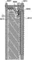
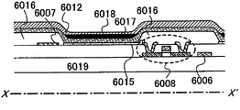
图7是说明本发明的半导体装置的截面图的图;7 is a diagram illustrating a cross-sectional view of a semiconductor device of the present invention;
图8是说明本发明的半导体装置的截面图的图;8 is a diagram illustrating a cross-sectional view of a semiconductor device of the present invention;
图9是说明本发明的半导体装置的截面图的图;9 is a diagram illustrating a cross-sectional view of a semiconductor device of the present invention;
图10是说明本发明的半导体装置的截面图的图;10 is a diagram illustrating a cross-sectional view of a semiconductor device of the present invention;
图11是说明本发明的半导体装置的俯视图的图;11 is a diagram illustrating a top view of a semiconductor device of the present invention;
图12是说明本发明的SOI基板的截面图;12 is a cross-sectional view illustrating an SOI substrate of the present invention;
图13是说明本发明的SOI基板的截面图;13 is a cross-sectional view illustrating an SOI substrate of the present invention;
图14是说明本发明的SOI基板的截面图;14 is a cross-sectional view illustrating an SOI substrate of the present invention;
图15是说明本发明的SOI基板的截面图;15 is a cross-sectional view illustrating an SOI substrate of the present invention;
图16是说明本发明的SOI基板的截面图;16 is a cross-sectional view illustrating an SOI substrate of the present invention;
图17是说明本发明的液晶显示装置的截面图;17 is a cross-sectional view illustrating a liquid crystal display device of the present invention;
图18是说明本发明的液晶显示装置的截面图;18 is a cross-sectional view illustrating a liquid crystal display device of the present invention;
图19是说明本发明的液晶显示装置的截面图;19 is a sectional view illustrating a liquid crystal display device of the present invention;
图20是说明本发明的液晶显示装置的结构的图;FIG. 20 is a diagram illustrating the structure of a liquid crystal display device of the present invention;
图21是说明本发明的液晶显示装置的截面图;21 is a sectional view illustrating a liquid crystal display device of the present invention;
图22是说明本发明的像素的电路图;Figure 22 is a circuit diagram illustrating a pixel of the present invention;
图23是说明本发明的像素的电路图;23 is a circuit diagram illustrating a pixel of the present invention;
图24是说明本发明的像素的电路图;Figure 24 is a circuit diagram illustrating a pixel of the present invention;
图25是说明本发明的像素的俯视图和截面图;Figure 25 is a top view and a cross-sectional view illustrating a pixel of the present invention;
图26是说明本发明的电子设备的图;FIG. 26 is a diagram illustrating an electronic device of the present invention;
图27是说明本发明的电子设备的图;FIG. 27 is a diagram illustrating an electronic device of the present invention;
图28是说明本发明的电子设备的图;FIG. 28 is a diagram illustrating an electronic device of the present invention;
图29是说明本发明的电子设备的图;FIG. 29 is a diagram illustrating an electronic device of the present invention;
图30是说明本发明的电子设备的图;30 is a diagram illustrating an electronic device of the present invention;
图31是说明本发明的电子设备的图;FIG. 31 is a diagram illustrating an electronic device of the present invention;
图32是说明本发明的电子设备的图;FIG. 32 is a diagram illustrating an electronic device of the present invention;
图33是说明本发明的电子设备的图;FIG. 33 is a diagram illustrating an electronic device of the present invention;
图34是说明本发明的电子设备的图;FIG. 34 is a diagram illustrating an electronic device of the present invention;
图35是说明本发明的电子设备的图;FIG. 35 is a diagram illustrating an electronic device of the present invention;
图36是说明本发明的电子设备的图;FIG. 36 is a diagram illustrating an electronic device of the present invention;
图37是说明本发明的电子设备的图;FIG. 37 is a diagram illustrating an electronic device of the present invention;
图38是说明本发明的电子设备的图;FIG. 38 is a diagram illustrating an electronic device of the present invention;
图39是说明本发明的电子设备的图。Fig. 39 is a diagram illustrating an electronic device of the present invention.
具体实施方式Detailed ways
以下参照附图说明本发明的实施方式。但是,本发明可以通过多种不同的方式来实施,本领域技术人员可以很容易地理解一个事实就是,在不脱离本发明的宗旨及其范围的情况下其方式和详细内容可以被变换为各种各样的形式。因此,本发明不应该被解释为仅限定在实施方式所记载的内容中。此外,在以下所说明的本发明的结构中,使用同一附图标记来表示不同附图之间的同一部分,并省略对同一部分或具有相同功能的部分的详细说明。Embodiments of the present invention will be described below with reference to the drawings. However, the present invention can be implemented in many different ways, and those skilled in the art can easily understand the fact that the modes and details can be changed into various forms without departing from the spirit and scope of the present invention. in various forms. Therefore, the present invention should not be interpreted as being limited only to the contents described in the embodiments. In addition, in the configuration of the present invention described below, the same reference numerals are used to designate the same parts between different drawings, and detailed descriptions of the same parts or parts having the same functions are omitted.
(实施方式1)(Embodiment 1)
在半导体装置或显示装置中,它们的全部或一部分由下述TFT构成:将硅层从单晶基板分离(剥离),并贴(复制)在玻璃基板上,从而在玻璃基板上形成的TFT;或者将单晶基板贴在玻璃基板上,利用从玻璃基板分离(剥离)单晶基板的方式在玻璃基板上形成硅层,从而在玻璃基板上形成的TFT。此外,将硅层从单晶基板分离,并将其贴在玻璃基板上,从而在玻璃基板上形成的TFT;或者将单晶基板贴在玻璃基板上,并利用将单晶基板分离的方式将单晶基板的硅层的一部分复制到玻璃基板上,从而在玻璃基板上形成的TFT,下面将它们称为单晶TFT。In semiconductor devices or display devices, all or part of them are composed of TFTs that are formed on a glass substrate by separating (peeling off) a silicon layer from a single crystal substrate and pasting (replicating) it on a glass substrate; Alternatively, a single crystal substrate is attached to a glass substrate, and a silicon layer is formed on the glass substrate by separating (peeling) the single crystal substrate from the glass substrate, thereby forming a TFT on the glass substrate. In addition, the silicon layer is separated from the single crystal substrate and attached to the glass substrate to form a TFT on the glass substrate; or the single crystal substrate is attached to the glass substrate and the single crystal substrate is separated. TFTs formed on the glass substrate by duplicating a part of the silicon layer of the single crystal substrate on the glass substrate are referred to as single crystal TFTs below.
然后,在形成单晶TFT的同时形成非单晶TFT。作为非单晶的例子,有非晶半导体((amorphous))、微晶半导体(也称为微晶体半导体、半非晶半导体、纳米晶半导体等)等。Then, the non-single-crystal TFT is formed simultaneously with the formation of the single-crystal TFT. Examples of non-single crystals include amorphous semiconductors (amorphous), microcrystalline semiconductors (also referred to as microcrystalline semiconductors, semi-amorphous semiconductors, nanocrystalline semiconductors, etc.), and the like.
接下来,将参照附图说明制造方法。Next, a manufacturing method will be described with reference to the drawings.
如图1(A)所示,绝缘基板101不局限于玻璃等,可以使用各种基板。例如,可以使用硼硅酸钡玻璃、硼硅酸铝玻璃等的玻璃基板、石英基板、陶瓷基板、或含有不锈钢的金属基板等。此外,也可以使用由以聚对苯二甲酸乙二醇酯(PET)、聚萘二甲酸乙二醇酯(PEN)、聚醚砜(PES)为代表的塑料或诸如丙烯酸等的具有柔性的合成树脂形成的基板。通过使用具有柔性的基板,可以制造可弯曲的半导体装置。如果是具有柔性的基板,则由于对基板的面积和形状方面没有特别限制,由此,作为绝缘基板101,如果使用例如一边长在1米以上且为矩形的基板,则可以显著提高生产率。与使用圆形硅基板的情况相比,该优点是极具优势的。As shown in FIG. 1(A), the insulating
另外,在绝缘基板101的表面等上,优选配置绝缘膜。该绝缘膜作为基底膜起作用。换而言之,防止来自绝缘基板101内部的诸如Na等的碱金属或碱土金属对半导体元件的特性造成负面影响。作为绝缘膜,可以使用包含氧或氮的绝缘膜的单层结构或层叠结构形成,包含氧或氮的绝缘膜例如是氧化硅(SiOx)、氮化硅(SiNx)、氧氮化硅(SiOxNy,x>y)或氮化氧化硅(SiNxOy,x>y)等。例如,当采用两层结构设置绝缘膜时,优选设置氮氧化硅膜作为第一层绝缘膜,并且设置氧氮化硅膜作为第二层绝缘膜。作为其它的例子,当采用三层结构设置绝缘膜时,优选设置氧氮化硅膜作为第一层绝缘膜,设置氮氧化硅膜作为第二层绝缘膜,并且设置氧氮化硅膜作为第三层绝缘膜。In addition, it is preferable to arrange an insulating film on the surface of the insulating
但是,不局限于此,也可以在绝缘基板101的表面上不配置绝缘膜。However, the present invention is not limited thereto, and an insulating film may not be disposed on the surface of the insulating
然后,在配置有绝缘膜等的绝缘基板101上配置半导体层102。半导体层102可以配置在绝缘基板101的整体表面上,也可以配置在绝缘基板101的一部分上。半导体层102优选是单晶。但是,不局限于此。因为单晶具有良好电流特性和高迁移率,所以这是优选的。Then, the
另外,对于半导体层102的配置方法等,在别的实施方式中进行说明。In addition, the method of arranging the
接下来,如图1(B)所示,为了使半导体层102成为规定的形状,通过刻蚀除去不需要的部分。换而言之,将半导体层102加工为岛形。换而言之,对半导体102形成图案。Next, as shown in FIG. 1(B), in order to make the
该半导体层102作为晶体管的激活层起作用。但是,不局限于此,有时作为电容元件的电极、电阻元件、二极管的激活层等起作用。This
接下来,如图1(C)所示,配置绝缘层103以使其覆盖半导体层102。绝缘层103通过使用CVD法、溅射法、热氧化法、气相淀积法、喷墨法及印刷法等进行配置。绝缘层103也可以作为栅绝缘膜起作用。另外,在将绝缘层103作为电容元件的绝缘体起作用时,绝缘层103有时作为层间膜起作用。Next, as shown in FIG. 1(C), an insulating
绝缘膜103可以使用下列膜的单层或层叠结构形成:硅氧烷树脂、氧化硅(SiOx)、氮化硅(SiNx)、氧氮化硅(SiOxNy,x>y)、氮氧化硅(SiNxOy,x>y)等的包含氧或氮的绝缘膜、DLC(类金刚石碳)等的包含碳的膜;或者环氧、聚酰亚胺、聚酰胺、聚乙烯苯酚、苯并环丁烯或丙烯酸等的有机材料。另外,硅氧烷树脂相当于包括Si-O-Si键的树脂。硅氧烷的骨架结构由硅(Si)和氧(O)的键构成。作为其取代基,可以使用至少包含氢的有机基(例如烷基或芳烃)。作为其取代基,也可以使用氟基。或者,也可以使用至少包含氢的有机基和氟基作为取代基。The insulating
但是,与半导体层102接触部分的绝缘层103优选是氧化硅(SiOx)。通过使用氧化硅(SiOx),可以防止电子被捕获且可以防止发生磁滞效果。However, the insulating
接下来,如图1(D)所示,配置导电层104以使其覆盖绝缘层103。导电层104通过使用CVD法、溅射法、热氧化法、气相淀积法、喷墨法及印刷法等进行配置。Next, as shown in FIG. 1(D), the
接下来,如图2(A)所示,通过蚀刻去除不需要的部分,以便使导电层104成为规定的形状。换而言之,将导电层104加工为岛状。也就是说,对导电层104形成图案。其结果,形成了栅电极104A和栅电极104B。Next, as shown in FIG. 2(A), unnecessary portions are removed by etching so that the
栅电极104A与半导体102及绝缘层103等一起构成晶体管203。因为栅电极104A配置于半导体102的上部,所以晶体管203成为顶栅型的晶体管。The
晶体管203可以采用多种结构。例如,晶体管203可以使用单漏极晶体管。在此情况下,因为可以通过简单的方法形成单漏极晶体管,所以它具有低制造成本和高成品率的优点。这里,半导体层102具有杂质浓度不同的区域,且具有沟道区、源区及漏区。通过这样控制杂质量,可以控制半导体层的电阻率。在源区及漏区中,可以使半导体层102和与其连接的导电膜之间的电学连接状态接近于欧姆接触。另外,作为分别形成杂质量彼此不同的半导体层的方法,可以使用以栅电极104A作为掩模对半导体层掺杂杂质的方法。The
另外,晶体管203可以形成为其栅电极104A具有一定程度以上的锥形角。在此情况下,因为可以通过简单的方法进行制造,所以它具有低制造成本和高成品率的优点。这里,半导体层102具有杂质浓度不同的区域,且具有沟道区、轻掺杂漏(Lightly Doped Drain:LDD)区、源区及漏区。通过这样控制杂质量,可以控制半导体层的电阻率。而且,可以使半导体层102和与其连接的导电膜之间的电学连接状态接近于欧姆接触。因为晶体管包括LDD区,所以在晶体管中不容易施加高的电场,可以抑制由于热载流子而导致的元件的退化。另外,作为分别形成杂质量不同的半导体层的方法,可以使用以栅电极104A作为掩模对半导体层掺杂杂质的方法。在栅电极104A具有一定程度以上的锥形角的情况下,可以提供通过栅电极104A掺杂到半导体层的杂质浓度的梯度,而且可以容易地形成LDD区。In addition, the
另外,在晶体管203中,栅电极104A可以至少由两层构成,且其下层栅电极比上层栅电极长。在此情况下,上层栅电极及下层栅电极的形状有时称为帽形。由于栅电极104A是帽形的,所以在不增加光掩模的情况下形成LDD区。另外,LDD区与栅电极104A重叠的结构特别称为GOLD结构(Gate Overlapped LDD)。再者,作为将栅电极104A的形状形成为帽形的方法,也可以使用下面的方法。In addition, in the
首先,当对栅电极104A形成图案时,通过干刻蚀来刻蚀下层栅电极及上层栅电极,使得其侧面形成为具有倾斜的形状(锥形)。然后,通过各向异性刻蚀,处理上层栅电极以使其倾角接近于垂直。通过该工序,形成了其截面形状为帽形的栅电极。然后,通过进行两次杂质元素的掺杂,形成沟道区、LDD区、源区及漏区。First, when patterning the
另外,将与栅电极104A重叠的LDD区称为Lov区,并且将不与栅电极104A重叠的LDD区称为Loff区。在此,Loff区在抑制截止电流值方面的效果高,而它在通过缓和漏极附近的电场来防止由于热载流子而导致的导通电流值的退化方面的效果低。另一方面,Lov区在通过缓和漏极附近的电场来防止导通电流值的退化方面的效果高,而它在抑制截止电流值方面的效果低。因此,优选在各种电路中制作具有对应于所需特性的结构的晶体管。例如,当使用半导体装置作为显示装置时,为了抑制截止电流值,像素晶体管优选使用具有Loff区的晶体管。另一方面,为了通过缓和漏极附近的电场来防止导通电流值的退化,外围电路中的晶体管优选使用具有Lov区的晶体管。In addition, the LDD region overlapping the
另外,作为晶体管203,可以形成具有与栅电极104A的侧面接触的侧壁的晶体管。当晶体管具有侧壁时,可以将与侧壁重叠的区域作为LDD区。In addition, as the
另外,作为晶体管203,可以通过使用掩模对半导体层102进行掺杂来形成LDD(Loff)区。通过这样,可以准确地形成LDD区,并且可以降低晶体管的截止电流值。In addition, as the
另外,作为晶体管203,可以通过使用掩模对半导体层进行掺杂来形成LDD(Lov)区。通过该方式,可以准确地形成LDD区,并且通过缓和晶体管的漏极附近的电场,可以降低导通电流值的退化。In addition, as the
另外,导电层104不局限于栅电极,也可以被加工为具有各种功能的导电膜。例如,导电层104可以具有用于形成存储电容的布线、用于形成扫描线的布线、用于连接电路的布线等的布线,以及电极等多种功能。In addition, the
下面,如图2(B)所示,设置绝缘层201以使其覆盖栅电极104A、栅电极104B。根据CVD法、溅射法、热氧化法、气相淀积法、喷墨法、印刷法等设置绝缘层201。绝缘层201也可作为栅绝缘膜起作用。此外,也可作为电容元件的绝缘体以及层间膜起作用。Next, as shown in FIG. 2(B), insulating
绝缘层201可以使用下列膜的单层或层叠结构形成:硅氧烷树脂、氧化硅(SiOx)、氮化硅(SiNx)、氧氮化硅(SiOxNy,x>y)、氮氧化硅(SiNxOy,x>y)等的包含氧或氮的绝缘膜、DLC(类金刚石碳)等的包含碳的膜;或者如环氧、聚酰亚胺、聚酰胺、聚乙烯苯酚、苯并环丁烯或丙烯酸等的有机材料等。再者,硅氧烷树脂相当于包括Si-O-Si键的树脂。硅氧烷的骨架结构由硅(Si)和氧(O)的键构成。作为其取代基,可以使用至少包含氢的有机基(例如烷基或芳烃)。也可以使用氟基作为取代基。或者,也可以使用至少包含氢的有机基和氟基作为取代基。The insulating
但是,与接下来要设置的半导体层202相接触的部分的绝缘层201优选采用氮化硅(SiNx)。半导体层202的内部有可能含有氢。此时,通过使用氮化硅(SiNx)作为绝缘层201,可以防止半导体层202所包含的氢与绝缘层201起反应。However, it is preferable to use silicon nitride (SiNx) for the insulating
接下来,如图2(C)所示,设置半导体层202以使其覆盖绝缘层201。根据CVD法、溅射法、热氧化法、气相淀积法、喷墨法、印刷法等设置半导体层202。半导体层202至少具有2层,在本征半导体上设置杂质半导体。Next, as shown in FIG. 2(C), a
半导体202的结晶度优选为非晶(amorphous)、微晶(也称为micro-crystal、半非晶、纳米晶体(nanocrystal))等。The crystallinity of the
下面,如图2(D)所示,为了将半导体层202形成为规定的形状,刻蚀去除不要的部分。也就是说,将半导体层202加工成岛形。即,对半导体层202形成图案。Next, as shown in FIG. 2(D), in order to form the
此时,作为形成图案后的半导体层,半导体层202A作为晶体管的激活层起作用。但是,不局限于此。也可将半导体层作为层间膜起作用。就是说,通过设置半导体层来减低布线的交叉电容,并且通过减少阶梯来减低布线的断裂。例如,半导体层202B及半导体层202C作为层间膜起作用。At this time, as a patterned semiconductor layer, the
下面,如图3(A)所示,设置导电层301以使其覆盖半导体层202A、半导体层202B、半导体层202C。根据CVD法、溅射法、热氧化法、气相淀积法、喷墨法、印刷法等设置导电层301。Next, as shown in FIG. 3(A), a
注意,导电层104、导电层301可以采用单层导电膜,或两层、三层的导电膜的叠层结构。作为导电层104的材料可以采用导电膜,例如,钽(Ta)、钛(Ti)、钼(Mo)、钨(W)、铬(Cr)、硅(Si)、铝(Al)、镍(Ni)、碳(C)、钨(W)、铂(Pt)、铜(Cu)、钽(Ta)、金(Au)、锰(Mn)等的元素的单体膜;或者上述元素的氮化膜(典型地,氮化钽膜、氮化钨膜或氮化钛膜);或者组合了上述元素的合金膜(典型地,Mo-W合金或Mo-Ta合金);或者上述元素的硅化物膜(典型地,钨硅化物膜或钛硅化物膜)等。或者,作为包含多个上述元素中的合金,可以使用包含C及Ti的Al合金、包含Ni的Al合金、包含C及Ni的Al合金、包含C及Mn的Al合金等。再者,上述的单体膜、氮化膜、合金膜、硅化物膜等可以具有单层结构或层叠结构。例如,在采用层跌结构的情况,可以采用将Al插入到Mo或Ti等之间的结构。通过采用该结构,可以提高Al对热或化学反应的耐受力。采用硅的情况下,为了提高导电性,优选包含多种杂质(P型杂质或N型杂质)。Note that the
接下来,如图3(B)所示,为了将导电层301形成为规定的形状,刻蚀去除不要的部分。也就是说,将导电层301加工成岛形。即,对导电层301形成图案。结果形成了导电层301A、导电层301B、导电层301C、导电层301D。导电层301A、导电层301B、导电层301C、导电层301D可作为源电极、漏电极、以及源极信号线等起作用。Next, as shown in FIG. 3(B), in order to form the
下面,如图3(C)所示,对半导体层202A的一部分进行刻蚀。由此,去除沟道区域的杂质层。结果完成晶体管303。由于栅电极104B设置在半导体层202A的下方,晶体管303既为底栅型晶体管,又是反交错型晶体管。另外,由于对沟道部分的半导体层进行了刻蚀,所以又是沟道刻蚀型晶体管。Next, as shown in FIG. 3(C), a part of the
半导体层202A可以使用非晶半导体、微晶半导体或半非晶半导体(SAS)形成。或者,也可以使用多晶半导体层。SAS是一种具有非晶结构和结晶结构(包括单晶、多晶)的中间结构且具有自由能稳定的第三状态的半导体,并且包括具有短程有序和晶格畸变的结晶区域。在SAS膜的至少一部分区域可以观察到0.5nm至20nm的结晶区域。当以硅为主要成分时,拉曼光谱向低于520cm-1波数的一侧偏移。在X射线衍射中,可以观察到来源于硅晶格的(111)和(220)的衍射峰。SAS至少包含1原子%以上的氢或卤素以补充悬空键。通过使材料气体辉光放电分解(等离子体CVD)形成SAS。作为材料气体,不仅可以使用SiH4,还可使用Si2H6、SiH2Cl2、SiHCl3、SiCl4、SiF4等。或者,也可以混合GeF4。该材料气体还可以用H2、或者H2与一种或多种选自He、Ar、Kr和Ne的稀有气体稀释。稀释比率为2倍至1000倍,压力大约为0.1Pa至133Pa,电源频率为1MHz至120MHz,优选为13MHz至60MHz。基板加热温度可以为300℃以下。作为膜中的杂质元素,来源于大气成分的杂质诸如氧、氮和碳等优选为1×1020cm-1以下。特别地,氧的浓度优选为5×1019/cm3以下,更优选为1×1019/cm3以下。这里,通过溅射法、LPCVD法或等离子体CVD法等、使用包含硅(Si)为其主要成分的材料(例如SixGe1-x等)形成非晶半导体层,然后,通过诸如激光晶化法、使用RTA或退火炉的热晶化法、或使用促进结晶的金属元素的热晶化法等的晶化法使该非晶半导体层结晶化。The
接下来,如图4(A)所示,配置绝缘层401以使其覆盖导电层301A、导电层301B、导电层301C及导电层C。绝缘层401通过使用CVD法、溅射法、热氧化法、气相淀积法、喷墨法及印刷法等进行配置。绝缘层401也作为保护膜起作用。另外,也在将绝缘膜401作为电容元件的绝缘体起作用时,绝缘膜401也有时用作层间膜。Next, as shown in FIG. 4(A), the insulating
绝缘层401可以使用下列膜的单层或叠层结构形成:硅氧烷树脂、氧化硅(SiOx)、氮化硅(SiNx)、氧氮化硅(SiOxNy,x>y)、氮氧化硅(SiNxOy,x>y)等的包含氧或氮的绝缘膜、DLC(类金刚石碳)等的包含碳的膜;或者如环氧、聚酰亚胺、聚酰胺、聚乙烯苯酚、苯并环丁烯或丙烯酸等的有机材料。另外,硅氧烷树脂相当于包括Si-O-Si键的树脂。硅氧烷的骨架结构由硅(Si)和氧(O)的键构成。作为其取代基,可以使用至少包含氢的有机基(例如烷基或芳烃)。也可以使用氟基作为取代基。或者,也可以使用至少包含氢的有机基和氟基作为取代基。The insulating
但是,与要配置的半导体层202接触部分的绝缘层401优选是氮化硅(SiNx)。半导体层202的内部有时含有氢。在此情况下,通过使用氮化硅(SiNx)作为绝缘层401,可以防止半导体层202所包含的氢与绝缘层401起反应。However, the insulating
再者,绝缘层401优选包含氮化硅(SiNx)。氮化硅(SiNx)具有阻挡杂质的功能。因此,可以保护晶体管免受杂质的影响。Furthermore, the insulating
另外,绝缘层401优选包含有机膜。由此,可以使绝缘层401的表面变得平坦。当绝缘层401的表面平坦时,也可以使形成于其上面的像素电极变得平坦。如果像素电极变得平坦,则可以适当地形成显示元件。In addition, the insulating
接下来,如图4(B)所示,形成接触孔。接触孔利用干刻蚀法或湿刻蚀法等、并通过刻蚀材料来形成。再者,当绝缘层401具有有机膜,且其有机膜由感光性材料形成时,可以与成膜同时形成接触孔。因此,不需要对接触孔部的材料进行刻蚀。所以,可以减少步骤数。接触孔501A、接触孔501B及接触孔501E通过刻蚀绝缘层401来形成。接触孔501C及接触孔501D通过刻蚀绝缘层401、绝缘层201及绝缘层103来形成。Next, as shown in FIG. 4(B), contact holes are formed. The contact hole is formed by etching a material using a dry etching method, a wet etching method, or the like. Furthermore, when the insulating
接下来,如图5所示,配置导电层601以使其覆盖绝缘层401、接触孔501A、接触孔501B、接触孔501C、接触孔501D、及接触孔501E。导电层601通过使用CVD法、溅射法、热氧化法、气相淀积法、喷墨法及印刷法等配置。导电层601作为布线、像素电极、透明电极及反射电极等起作用。Next, as shown in FIG. 5 , the
另外,导电层601可以为由单层的导电膜或两层、三层的导电膜的叠层结构。而且,导电层601优选具有高透光率,且具有透明或接近透明的区域。因此,导电层601可以用作透光区域的像素电极。另外,导电层601优选具有反射率高的区域。因此,导电层601可以用作反射区域的像素电极。In addition, the
另外,导电层601优选为包含ITO、IZO及ZnO等的膜。In addition, the
接下来,如图6所示,通过刻蚀除去不需要的部分以使导电层601形成为规定的形状。换而言之,将导电层601加工为岛形。换而言之,对导电层601形成图案。Next, as shown in FIG. 6 , unnecessary portions are removed by etching so that the
在这种情况下,作为形成图案后的导电层,导电层601A作为像素电极起作用。但是,不局限于此。此外,导电层601B及导电层601C作为布线起作用。导电层601B具有连接导电层301C和半导体层102的功能。导电层601C具有连接导电层301D和半导体层102的功能。In this case, as a patterned conductive layer, the
之后,与各种显示元件相吻合,经过各种工序完成显示装置。例如,形成定向膜,并且在与具有彩色滤光片的相对基板之间配置液晶。或者,在导电层601A之上配置有机EL材料,并在其上配置阴极。Afterwards, the display device is completed through various processes in accordance with various display elements. For example, an alignment film is formed, and a liquid crystal is disposed between an opposing substrate having a color filter. Alternatively, an organic EL material is disposed on the
此外,虽然在图4(B)中,通过形成接触孔并在其上配置导电层,从而连接导电层301C和半导体层102,但是如图7所示,也可以通过接触孔501F及接触孔501G并使用导电层601D,实现连接导电层301F和导电层104C。另外,导电层301F由导电层301形成,导电层104C由导电层104形成,导电层601D由导电层601形成。接触孔501F及接触孔501G与接触孔501A、接触孔501B、接触孔501C、接触孔501D等同时形成。In addition, although in FIG. 4(B), the
此外,既可以如导电层301C、导电层301D、导电层301F等,在它们的下面配置半导体层,又可以如图7所示,在导电层301E的下面不配置半导体层。In addition, a semiconductor layer may be disposed under the
再者,在图2(D)、图3(A)、图3(B)、图3(C)中,通过使用不同的掩模(中间掩模)对半导体层202和导电层301形成图案,但是不局限于此。通过采用半色调掩模、灰度掩模等,可以利用一个掩模(中间掩模)对半导体层202和导电层301形成图案。图8示出了该情况的截面图。由于使用半色调掩模、灰度掩模等,因此半导体层202E的尺寸比导电层301A、导电层301B的尺寸大。换而言之,在导电层301A、导电层301B的下面,一定配置有半导体层202E。Furthermore, in FIG. 2(D), FIG. 3(A), FIG. 3(B), and FIG. 3(C), the
另外,虽然在图6中,通过导电层601B、电层601C连接导电层301C及半导体层102,并且连接导电层301D及半导体层102,并且在图7中,通过导电层601D连接导电层301F及导电层104C,但不局限于此。也可以不通过其他的导电膜,而通过形成接触孔来直接进行连接。也就是说,作为图2(B)的下一步骤,或者作为图2(D)的下一步骤,可以通过对绝缘层201、绝缘层103进行刻蚀来形成接触孔,从而将使用导电层301形成的导电膜、与使用导电层104形成的导电膜或使用半导体层102形成的半导体层实现直接连接。图9表示了这种情况的示例。在图9中,使用导电层301形成的导电层301G及半导体层102通过接触孔901A实现直接连接。同样,使用导电层301形成的导电层301H及半导体层102通过接触孔901B实现直接连接。并且,导电层601E通过接触孔501H与导电层301H实现直接连接。另外,在这种情况下,关于导电层301H及导电层301G,优选在其下方不设置半导体层。这是因为当与半导体层102接触时,导电层301H及301G与半导体层102之间优选没有其他的层。In addition, although in Figure 6, the
另外,在图6中,晶体管303虽然为沟道蚀刻型,但是不局限于此。也可以使用沟道保护型。图10表示了这种情况的示例。在沟道保护型中,不是连续设置半导体层,而在其中间设置用来保护沟道部分的刻蚀的绝缘层1001。也就是说,在本征半导体层1002的上方设置绝缘层1001,在其上,设置半导体层1003A及半导体层1003B。在半导体层1003A及半导体层1003B中,包含杂质(N型或者P型)。In addition, in FIG. 6, although the
另外,在图10中,对半导体层1002形成图案,其后,对半导体层1003A、半导体层1003B、导电层301A及导电层301B同时形成图案,但是不局限于此。也可以对半导体层1002、半导体层1003A、半导体层1003B、导电层301A及导电层301B同时形成图案。这种情况下,在导电层301A及导电层301B的下方必须设置有半导体层1002。In addition, in FIG. 10 , the
以上说明了晶体管的结构及晶体管的制造方法。注意,布线、电极、导电层、导电膜、端子、通路、插头等优选从由铝(Al)、钽(Ta)、钛(Ti)、钼(Mo)、钨(W)、钕(Nd)、铬(Cr)、镍(Ni)、铂(Pt)、金(Au)、银(Ag)、铜(Cu)、镁(Mg)、钪(Sc)、钴(Co)、锌(Zn)、铌(Nb)、硅(Si)、磷(P)、硼(B)、砷(As)、镓(Ga)、铟(In)、锡(Sn)和氧(O)构成的族中选择的一个或多个元素、或者以从上述族中选择的一个或多个元素作为成分的化合物、合金材料(例如,氧化铟锡(ITO)、氧化铟锌(IZO)、包含氧化硅的氧化铟锡(ITSO)、氧化锌(ZnO)、氧化锡(SnO)、氧化锡镉(CTO)、铝钕(Al-Nd)、镁银(Mg-Ag)、钼铌(Mo-Nb)等)来形成。或者,优选形成布线、电极、导电层、导电膜、端子等,以包含组合上述化合物而成的物质等。或者,优选形成布线、电极、导电层、导电膜、端子等,以包含由选自上述族中的一个或多个元素和硅构成的化合物(硅化物)(例如,铝硅、钼硅、硅化镍等)、由选自上述群中的一个或多个元素和氮构成的化合物(例如,氮化钛、氮化钽、氮化钼等)。The structure of the transistor and the method of manufacturing the transistor have been described above. Note that wiring, electrodes, conductive layers, conductive films, terminals, vias, plugs, etc. are preferably made of aluminum (Al), tantalum (Ta), titanium (Ti), molybdenum (Mo), tungsten (W), neodymium (Nd) , chromium (Cr), nickel (Ni), platinum (Pt), gold (Au), silver (Ag), copper (Cu), magnesium (Mg), scandium (Sc), cobalt (Co), zinc (Zn) , niobium (Nb), silicon (Si), phosphorus (P), boron (B), arsenic (As), gallium (Ga), indium (In), tin (Sn) and oxygen (O) One or more elements, or compounds containing one or more elements selected from the above groups as components, alloy materials (for example, indium tin oxide (ITO), indium zinc oxide (IZO), indium oxide containing silicon oxide Tin (ITSO), zinc oxide (ZnO), tin oxide (SnO), tin cadmium oxide (CTO), aluminum neodymium (Al-Nd), magnesium silver (Mg-Ag), molybdenum niobium (Mo-Nb), etc.) form. Alternatively, it is preferable to form wirings, electrodes, conductive layers, conductive films, terminals, and the like to include combinations of the above-mentioned compounds, and the like. Alternatively, it is preferable to form wirings, electrodes, conductive layers, conductive films, terminals, etc. so as to contain compounds (silicides) composed of one or more elements selected from the above-mentioned groups and silicon (for example, aluminum silicon, molybdenum silicon, silicide nickel, etc.), compounds consisting of one or more elements selected from the above group and nitrogen (for example, titanium nitride, tantalum nitride, molybdenum nitride, etc.).
硅(Si)也可以包含n型杂质(磷等)或p型杂质(硼等)。由于硅包含杂质,可以提高导电率,并且可以实现类似于普通导体的功能。于是,可以更容易地使用于布线、电极等。Silicon (Si) may also contain n-type impurities (phosphorus, etc.) or p-type impurities (boron, etc.). Since silicon contains impurities, the conductivity can be improved and it can function like a normal conductor. Therefore, it can be more easily used for wiring, electrodes, and the like.
另外,作为硅可以使用具有各种结晶性的硅,诸如单晶硅、多晶硅、微晶硅等。或者,作为硅也可以使用没有结晶性的硅诸如非晶硅等。通过使用单晶硅或多晶硅,可以降低布线、电极、导电层、导电膜、端子等的电阻。通过使用非晶硅或微晶硅,可以利用简单工序来形成布线等。In addition, silicon having various crystallinities such as single crystal silicon, polycrystalline silicon, microcrystalline silicon, and the like can be used as silicon. Alternatively, silicon having no crystallinity such as amorphous silicon or the like may also be used as silicon. By using single crystal silicon or polycrystalline silicon, the resistance of wiring, electrodes, conductive layers, conductive films, terminals, and the like can be reduced. By using amorphous silicon or microcrystalline silicon, wiring and the like can be formed with a simple process.
再者,由于铝或银具有高导电率,所以可以减少信号延迟。再者,由于铝或银容易被刻蚀,所以可以容易地形成图案并对它们进行细微加工。Also, since aluminum or silver has high conductivity, signal delay can be reduced. Furthermore, since aluminum or silver is easily etched, it is possible to easily form patterns and microfabricate them.
再者,由于铜具有高导电率,所以可以减少信号延迟。当使用铜时,由于优选采用层叠结构,以便提高紧密性。Furthermore, since copper has high conductivity, signal delay can be reduced. When copper is used, it is preferable to adopt a laminated structure in order to improve compactness.
钼或钛具有如下优点:即使钼或钛与氧化物半导体(ITO、IZO等)或硅接触也不会产生缺陷,容易被蚀刻,具有高耐热性等有点。所以优选使用钼或钛。Molybdenum or titanium has advantages such as no defects occurring even if molybdenum or titanium contacts oxide semiconductors (ITO, IZO, etc.) or silicon, easy etching, and high heat resistance. Molybdenum or titanium are therefore preferably used.
由于钨具有高耐热性等的优点,所以优选使用钨。Since tungsten has advantages such as high heat resistance, tungsten is preferably used.
由于钕具有高耐热性等的优点,所以优选使用钕。特别地,优选使用钕和铝的合金,因为耐热性提高并且铝难以产生小丘。Neodymium is preferably used because it has advantages such as high heat resistance. In particular, an alloy of neodymium and aluminum is preferably used because heat resistance improves and aluminum hardly generates hillocks.
硅具有如下优点:可以与晶体管所具有的半导体层同时形成,具有高耐热性等。所以优选使用硅。Silicon has advantages in that it can be formed simultaneously with a semiconductor layer of a transistor, has high heat resistance, and the like. Silicon is therefore preferably used.
由于ITO、IZO、ITSO、氧化锌(ZnO)、硅(Si)、氧化锡(SnO)、氧化锡镉(CTO)具有透光性,所以可以使用于使光透过的部分。例如,它们可以用作于像素电极或共同电极。ITO, IZO, ITSO, Zinc Oxide (ZnO), Silicon (Si), Tin Oxide (SnO), and Cadmium Tin Oxide (CTO) are light-transmitting, so they can be used in parts that transmit light. For example, they can be used as pixel electrodes or common electrodes.
优选使用IZO,因为IZO容易被刻蚀和加工。在刻蚀IZO时,难以留下渣滓。因而,当IZO用作像素电极时,可以减少液晶元件或发光元件发生不良情况(短路、取向无序等)。IZO is preferably used because IZO is easily etched and processed. When etching IZO, it is difficult to leave dross. Therefore, when IZO is used as a pixel electrode, occurrence of defects (short circuit, alignment disorder, etc.) in liquid crystal elements or light emitting elements can be reduced.
另外,布线、电极、导电层、导电膜、端子、通路、插头等可以具有单层结构或多层结构。通过采用单层结构,布线、电极、导电层、导电膜、端子等的制造工序可以简化、可以减少工序数目,并且可以减少成本。或者,通过采用多层结构,可以在有效地利用各材料的优点的同时,减少缺点,以形成性能好的布线、电极等。例如,通过在多层结构中包括低电阻材料(铝等),可以谋求实现布线电阻的降低。作为其它的例子,通过采用用高耐热性材料夹住低耐热性材料的层叠结构,可以在有效地利用低耐热性材料所具有的优点的同时,提高布线、电极等的耐热性。例如,优选采用用含有钼、钛、钕等的层夹住包含铝的层的层叠结构。In addition, wiring, electrodes, conductive layers, conductive films, terminals, vias, plugs, and the like may have a single-layer structure or a multi-layer structure. By adopting a single-layer structure, manufacturing processes of wiring, electrodes, conductive layers, conductive films, terminals, etc. can be simplified, the number of processes can be reduced, and costs can be reduced. Alternatively, by adopting a multilayer structure, it is possible to effectively utilize the advantages of each material while reducing disadvantages to form wiring, electrodes, etc. with good performance. For example, by including a low-resistance material (aluminum, etc.) in the multilayer structure, reduction in wiring resistance can be sought. As another example, by adopting a laminated structure in which materials with low heat resistance are sandwiched between materials with high heat resistance, the heat resistance of wiring, electrodes, etc. can be improved while effectively utilizing the advantages of materials with low heat resistance. . For example, it is preferable to employ a laminated structure in which layers containing aluminum are sandwiched by layers containing molybdenum, titanium, neodymium, or the like.
在布线、电极等彼此直接接触的情况下,它们有时对彼此会有不利的影响。例如,一个布线、电极等材料混合到另一个布线、电极等中并改变其性质,于是使其不能发挥本来的作用。作为另一例子,当形成或制造高电阻部分时,出现问题,而不能正常地制造。在此情况下,优选通过采用层叠结构用难以反应的材料夹住容易反应的材料,或者利用难以反应的材料来覆盖容易反应的材料。例如,当使ITO与铝连接时,优选在ITO与铝之间插入钛、钼、钕的合金。作为另一例子,当使硅与铝连接时,优选在硅与铝之间插入钛、钼、钕的合金。In the case where wirings, electrodes, etc. are in direct contact with each other, they sometimes have an adverse effect on each other. For example, a material of one wiring, electrode, etc. is mixed into another wiring, electrode, etc. and changes its properties, thus making it unable to perform its original function. As another example, when forming or manufacturing a high-resistance portion, a problem occurs and cannot be normally manufactured. In this case, it is preferable to sandwich the easily reactive material with the difficultly reactive material by adopting a laminated structure, or to cover the easily reactive material with the difficultly reactive material. For example, when connecting ITO to aluminum, it is preferable to insert an alloy of titanium, molybdenum, or neodymium between ITO and aluminum. As another example, when connecting silicon and aluminum, it is preferable to insert an alloy of titanium, molybdenum, or neodymium between silicon and aluminum.
布线是指配置导电体后得到的部分。导电体既可以配置为长线状,又可以配置为短线状。因此,电极包括在布线中。The wiring refers to a portion obtained by arranging conductors. The conductors may be arranged in the form of long lines or in the form of short lines. Therefore, electrodes are included in the wiring.
也可以使用碳纳米管作为布线、电极、导电层、导电膜、端子、通路、插头等。而且,由于碳纳米管具有透光性,所以碳纳米管可以使用于使光透过的部分。例如,碳纳米管可以使用于像素电极或共同电极。Carbon nanotubes can also be used as wiring, electrodes, conductive layers, conductive films, terminals, vias, plugs, and the like. Furthermore, since carbon nanotubes have light-transmitting properties, carbon nanotubes can be used in parts that transmit light. For example, carbon nanotubes can be used for pixel electrodes or common electrodes.
以上示出了截面图,接下来将示出布局图。图11示出配置有两个晶体管203的布局图。通过在半导体层102AA和半导体层102BB上配置栅电极104AA来形成晶体管。第一电源线301AA和半导体层102AA通过接触孔并使用导电层601AA来实现彼此连接。同样,第二电源线301CC和半导体层102BB通过接触孔并使用导电层601CC来实现彼此连接。输出布线301BB通过接触孔501AA及接触孔501BB并使用导电层601BB与半导体层102AA及半导体层102BB来实现彼此连接。A sectional view is shown above, and a layout view will be shown next. FIG. 11 shows a layout diagram in which two
另外,图11所示的电路可以作为反相器电路或源极跟随电路进行工作。In addition, the circuit shown in FIG. 11 can operate as an inverter circuit or a source follower circuit.
通过这样,由于晶体管具有高迁移率和高电流供给能力,所以使用晶体管203而构成的电路优选用作驱动电路。另一方面,因为晶体管303是迁移率不高且可以在大面积上制造,所以优选用作像素电路。Through this, since the transistor has high mobility and high current supply capability, a circuit configured using the
另外,在本实施方式中参照各种附图进行了说明,但是各附图所示的内容(或其一部分)相对于其他附图所示的内容(或其一部分),可以自由地进行适用、组合、或置换等。再者,在如上所示的附图中,关于各个部分可以通过组合其他部分来构成更多附图。In addition, although the present embodiment has been described with reference to various drawings, the content (or a part thereof) shown in each drawing can be freely applied to the content (or a part thereof) shown in other drawings. Combination, or replacement, etc. Furthermore, in the drawings shown above, more drawings can be constituted by combining other parts with respect to each part.
与此同样,本实施方式的各附图所示的内容(或其一部分)相对于其他实施方式的附图所示的内容(或其一部分),可以自由地进行适用、组合、或置换等。再者,在本实施方式的附图中,关于各个部分,可以通过组合其他实施方式的部分来构成更多附图。Similarly, the content (or part thereof) shown in each drawing of this embodiment can be freely applied, combined, or substituted with respect to the content (or part thereof) shown in the drawings of other embodiments. In addition, in the drawings of this embodiment, regarding each part, it is possible to configure more drawings by combining parts of other embodiments.
此外,本实施方式表示其他实施方式所述的内容(或其一部分)的具体例子、其稍微变形的例子、变更一部分后的例子、改良后的例子、详细描述后的例子、应用后的例子、具有相关部分的例子等。因此,其他实施方式所述的内容可以对本实施方式所述的内容自由地进行适用、组合、或置换。In addition, this embodiment shows a specific example of the content (or part thereof) described in other embodiments, a slightly modified example, a partly modified example, an improved example, a detailed description example, an applied example, Examples etc. with relevant sections. Therefore, the contents described in other embodiments may be freely applied, combined, or replaced with the contents described in this embodiment.
(实施方式2)(Embodiment 2)
接下来,下面对于单晶TFT中所使用的半导体层的配置方法进行说明。Next, a method of arranging a semiconductor layer used in a single crystal TFT will be described below.
本发明的SOI基板的结构示出于图12(A)和图12(B)。在图12(A)中支撑基板9200为具有绝缘表面的基板或绝缘基板,可以应用铝硅酸盐玻璃、铝硼硅酸盐玻璃、钡硼硅酸盐玻璃等的用于电子工业中的各种玻璃基板。此外还可以使用石英玻璃、硅片等半导体基板。SOI层9202为单晶半岛体层,典型使用单晶硅。此外,可以使用于利用氢离子注入剥离法从硅或锗的单晶半导体基板或多晶半导体基板剥离的半导体层。另外还可以使用由镓砷、磷化铟等化合物半导体所形成的晶体半导体层。The structure of the SOI substrate of the present invention is shown in FIG. 12(A) and FIG. 12(B). In FIG. 12(A), the
在这种支撑基板9200和SOI层9202之间,设置具有平滑面且形成亲水性表面的键合层9204。作为该键合层9204适用氧化硅膜。特别优选的是使用有机硅烷气体且利用化学气相成长法而制造的氧化硅膜。作为有机硅烷气体可以使用含有硅的化合物,如四乙氧基硅烷(TEOS:化学式Si(OC2H5)4)、四甲基硅烷(TMS)、四甲基环四硅氧烷(TMCTS)、八甲基环四硅氧烷(OMCTS)、六甲基二硅氮烷(HMDS)、三乙氧基硅烷(化学式SiH(OC2H5)3)、三(二甲基氨基)硅烷(化学式SiH(N(CH3)2)3)等。Between such a
将上述具有平滑面并形成亲水性表面的键合层9204设为5nm至500nm的厚度。该厚度可以使被淀积的膜表面的表面粗糙平滑化,并且可以确保该膜的成长表面的平滑性。另外,可以缓和支撑基板9200和SOI层9202的应变。也可以在支撑基板9200上设置同样的氧化硅膜。即,当将SOI层9202键合到具有绝缘表面的基板或者绝缘性的支撑基板9200时,在形成键合的面的一方或双方上,通过设置以有机硅烷为原材料且淀积了的氧化硅膜构成的键合层9204,可以形成坚固键合。The
图12(B)表示在支撑基板9200上设置阻挡层9205和键合层9204的结构。当将SOI层9202键合到支撑基板9200时,可以防止如碱金属或碱土金属那样的可动离子杂质从用作支撑基板9200的玻璃基板扩散以污染SOI层9202。此外,适当地设置支撑基板9200一侧的键合层9204即可。FIG. 12(B) shows a structure in which a
图13(A)表示在SOI层9202和键合层9204之间设置含有氮的绝缘层9220的构成。含有氮的绝缘层9200是通过对选自氮化硅膜、氮氧化硅膜、或者氧氮化硅膜中的一种或多种的膜进行层叠而构成的。例如,可以从SOI层9202一侧层叠氧氮化硅膜、氮氧化硅膜来形成含有氮的绝缘层9220。为了形成与支撑基板9200的键合而设置键合层9204。与此相对,优选设置含有氮的绝缘层9220,以便防止可动离子或水分等的杂质扩散到SOI层9202且污染SOI层9202。FIG. 13(A) shows a configuration in which an insulating
另外,在此氧氮化硅膜是指如下膜:在组成方面氧的含量比氮的含量多,作为浓度范围,例如包含50原子%至70原子%的氧、0.5原子%至15原子%的氮、25原子%至35原子%的硅、0.1原子%至10原子%的氢。另外,氮氧化硅膜是指如下膜:在组成方面氮的含量比氧的含量多且当使用RBS及HFS测量时,作为浓度范围,例如包含5原子%至30原子%的氧、20原子%至55原子%的氮、25原子%至35原子%的Si、10原子%至30原子%的氢。但是,上述范围都是在使用卢瑟福背散射光谱学法(RBS:RutherfordBackscattering Spectrometry)以及氢前方散射法(HFS:Hydrogen ForwardScattering)进行测量的情况下得到的结果。另外,将构成元素的总计设为不超过100原子%。Here, the silicon oxynitride film refers to a film that contains more oxygen than nitrogen in terms of composition, and the concentration range includes, for example, 50 atomic % to 70 atomic % of oxygen, 0.5 atomic % to 15 atomic % of Nitrogen, 25 to 35 atomic % silicon, 0.1 to 10 atomic % hydrogen. In addition, the silicon oxynitride film refers to a film that contains more nitrogen than oxygen in terms of composition, and when measured using RBS and HFS, the concentration range includes, for example, 5 atomic % to 30 atomic % of oxygen, 20 atomic % Nitrogen to 55 atomic %, Si from 25 atomic % to 35 atomic %, hydrogen from 10 atomic % to 30 atomic %. However, the above-mentioned ranges are the results obtained when measurements are performed using Rutherford Backscattering Spectrometry (RBS: Rutherford Backscattering Spectrometry) and Hydrogen Forward Scattering (HFS: Hydrogen Forward Scattering). In addition, the total of the constituent elements is made not to exceed 100 atomic %.
图13(B)表示在支撑基板9200上设置键合层9204的构成。优选在支撑基板9200和键合层9204之间设有阻挡层9205。因此可以防止如碱金属或碱土金属那样的可动离子杂质从用作支撑基板9200的玻璃基板扩散且污染SOI层9202。另外,在SOI层9202上形成有氧化硅膜9221。该氧化硅膜9221与键合层9204形成键合,从而在支撑基板9200上固定SOI层。作为氧化硅膜9221优选通过热氧化而形成的结构。此外,也可以与键合层9204一样使用TEOS且通过化学气相成长法而形成的膜。另外,作为氧化硅膜9221可以使用化学氧化物。例如可以通过利用含臭氧的水对半导体基板表面进行处理来形成化学氧化物。优选形成化学氧化物以反映半导体基板的平坦性。FIG. 13(B) shows a configuration in which a
对这种SOI基板的制造方法参照图14(A)至图14(C)和图15进行说明。A method of manufacturing such an SOI substrate will be described with reference to FIGS. 14(A) to 14(C) and FIG. 15 .
图14(A)所示的半导体基板9201被清洗,并且从其表面将以电场经过加速后的离子导入到规定的深度,从而形成脆化层9203。进行离子的照射及导入要考虑形成于支撑基板上的SOI层的厚度。该SOI层的厚度为5nm至500nm,优选为10nm至200nm。导入离子时的加速电压要考虑这种厚度,从而将厚度设定为离子导入到半导体基板9201。脆化层通过导入以氦或以氟为代表的卤素的离子来形成。在此情况下,优选使用由一种或多种相同的原子构成的质量不同的离子。当照射氢离子时,该氢离子优选包含H+、H2+、H3+离子且将H3+离子的比率提高。通过提高H3+离子的比率,可以提高照射效率,从而可以缩短照射时间。利用这样的结构可以容易地进行分离。The
在以高剂量条件照射离子的情况下,有时半导体基板9201的表面会变得粗糙。因此也可以在照射离子后的表面上利用氮化硅膜或氮氧化硅膜等进行设置,且相对于照射离子的保护膜,其厚度为50nm至200nm。When ions are irradiated under high-dose conditions, the surface of the
其次,如图14(B)所示,在与支撑基板形成键合的面上形成氧化硅膜作为键合层9204。作为氧化硅膜,如上所述,使用有机硅烷气体且通过化学气相成长法来制造的氧化硅膜是优选的。另外也可以采用使用硅烷气体且通过化学气相成长法来制造的氧化硅膜。在利用化学气相成长法进行的成膜中,作为从形成于单晶半导体基板上的脆化层9203不发生脱气的温度,采用例如350℃以下的淀积温度。另外,作为从单晶或多晶半导体基板分离SOI层的热处理采用比淀积温度高的热处理温度。Next, as shown in FIG. 14(B), a silicon oxide film is formed as a
图14(C)表示使支撑基板9200与形成半导体基板9201的键合层9204的表面密接,且使两者键合起来的情况。对形成键合的面进行充分清洗。然后通过使支撑基板9200和键合层9204密接以形成键合。范德瓦耳斯力作用于该键合,并且通过压接支撑基板9200和半导体基板9201,从而可以利用氢耦合来形成更坚固的键合。FIG. 14(C) shows a case where the
为了形成良好的键合,也可以使表面活化。例如,对形成键合的面照射原子束或离子束。当利用原子束或离子束时,可以使用氩等惰性气体中性原子束或惰性气体离子束。另外,进行等离子体照射或自由基处理。通过这种表面处理,即使在温度为200℃至400℃的情况下也可以容易地形成异种材料之间的键合。In order to form a good bond, the surface can also be activated. For example, an atomic beam or an ion beam is irradiated to the bonded surface. When using an atomic beam or an ion beam, an inert gas neutral atom beam such as argon or an inert gas ion beam can be used. In addition, plasma irradiation or radical treatment is performed. With this surface treatment, bonding between dissimilar materials can be easily formed even at a temperature of 200°C to 400°C.
在中间夹着键合层9204而贴合支撑基板9200和半导体基板9201之后,优选进行加热处理或加压处理。通过进行加热处理或加压处理,可以提高键合强度。加热处理的温度优选为支撑基板9200的耐热温度以下。在加压处理中,对于键合面施加向垂直方向的压力,且考虑支撑基板9200及半导体基板9201的耐压性,从而进行该处理。After bonding the
在图15中,在将支撑基板9200和半导体基板9201贴合之后,进行热处理,从而在脆化层9203处分离半导体基板9201。热处理的温度优选为键合层9204的成膜温度以上且支撑基板9200的耐热温度以下。例如,通过进行400℃至600℃的热处理,形成于脆化层9203中的微小空洞发生堆积变化,因而可以沿着脆化层9203进行分离(劈开)。因为键合层9204与支撑基板9200键合,所以在支撑基板9200上残留具有与半导体基板9201相同的结晶性的SOI层9202。In FIG. 15 , after bonding the
图16示出在支撑基板一侧设置键合层以形成SOI层的工序。图16(A)示出将对于形成有氧化硅膜9221的半导体基板9201将以电场加速后的离子导入到规定的深度以形成脆化层9203的工序。关于氢、氦或以氟为代表的卤素的离子的导入与图14(A)的情况相同。通过在半导体基板9201的表面形成氧化硅膜9221,可以防止由照射离子而使表面受损伤、从而使其平坦性恶化的情况。FIG. 16 shows a step of forming an SOI layer by providing a bonding layer on the support substrate side. FIG. 16(A) shows a step of introducing ions accelerated by an electric field to a predetermined depth into a
图16(B)示出形成有阻挡层9225及键合层9204的支撑基板9200、与半导体基板9201的形成有氧化硅膜9221的一面密接而形成键合的工序。通过使支撑基板9200上的键合层9204与半导体基板9201的氧化硅膜9221密接来形成键合。16(B) shows a step in which the
之后,如图16(C)所示,分离半导体基板9201。与图15的情况一样地进行分离半导体基板的热处理。如此可以获得图13(B)所示的SOI基板。After that, as shown in FIG. 16(C), the
通过这样,根据本方式,即使在使用玻璃基板等的耐热温度为700℃以下的支撑基板9200的情况下,也可以获得耦合部的粘接力坚固的SOI层9202。作为支撑基板9200可以使用铝硅酸盐玻璃、铝硼硅酸盐玻璃、钡硼硅酸盐玻璃等被称为无碱玻璃的用于电子工业中的各种玻璃基板。即,可以在一边超过一米的基板上形成单晶半导体层。通过使用这种大面积基板,不仅可以制造液晶显示器等显示装置,而且还可以制造半导体集成电路。Thus, according to this aspect, even when using a
再者,半导体层的制造方法和配置方法不局限于此。也可以通过CVD法等在绝缘基板上对非晶硅进行成膜,然后通过照射激光(线状激光、连续固体振荡激光等)、或者进行加热等的方式对该非晶硅进行结晶化,从而制造多晶硅或微晶硅。Furthermore, the manufacturing method and arrangement method of the semiconductor layer are not limited thereto. It is also possible to form a film of amorphous silicon on an insulating substrate by the CVD method, and then crystallize the amorphous silicon by irradiating laser light (line laser, continuous solid-state oscillator laser, etc.) or heating. Manufacture of polysilicon or microcrystalline silicon.
另外,在本实施方式中参照各种附图进行了说明,但是各附图所示的内容(或其一部分)相对于其他附图所示的内容(或其一部分),可以自由地进行适用、组合、或置换等。再者,在如上所示的附图中,关于各个部分,可以通过组合其他部分来构成更多附图。In addition, although the present embodiment has been described with reference to various drawings, the content (or a part thereof) shown in each drawing can be freely applied to the content (or a part thereof) shown in other drawings. Combination, or replacement, etc. Also, in the drawings shown above, regarding each part, more drawings can be constituted by combining other parts.
与此同样,本实施方式的各附图所示的内容(或其一部分)相对于其他实施方式的附图所示的内容(或其一部分),可以自由地进行适用、组合、或置换等。再者,在本实施方式的附图中,关于各个部分,可以通过组合其他实施方式的部分来构成更多附图。此外,本实施方式表示其他实施方式所述的内容(或其一部分)的具体例子、其稍微变形后的例子、变更其一部分后的例子、改良后的例子、详细描述后的例子、应用后的例子、具有相关部分的例子等。因此,其他实施方式所述的内容相对于本实施方式所述的内容自由地进行适用、组合、或置换。Similarly, the content (or part thereof) shown in each drawing of this embodiment can be freely applied, combined, or substituted with respect to the content (or part thereof) shown in the drawings of other embodiments. In addition, in the drawings of this embodiment, regarding each part, it is possible to configure more drawings by combining parts of other embodiments. In addition, this embodiment shows a specific example of the content (or a part thereof) described in other embodiments, a slightly modified example, a partly modified example, an improved example, a detailed description example, and an applied example. Examples, examples with related sections, etc. Therefore, the contents described in other embodiments can be freely applied, combined, or replaced with respect to the contents described in this embodiment.
(实施方式3)(Embodiment 3)
本实施方式中,说明液晶面板的外围部分。In this embodiment, the peripheral portion of the liquid crystal panel will be described.
图17示出了包括被称为边缘照明型的背光灯单元5201和液晶面板5207的液晶显示装置的一个例子。边缘照明型是指在背光灯单元的端部配置光源且光源的荧光从整个发光表面发射的类型。边缘照明型的背光灯单元很薄且可以节省耗电量。FIG. 17 shows an example of a liquid crystal display device including a so-called edge-light
背光灯单元5201由扩散板5202、导光板5203、反射板5204、灯反射器5205、以及光源5206构成。The
光源5206具有根据需要发光的功能。例如,作为光源5206,可以使用冷阴极管、热阴极管、发光二极管、无机EL元件或有机EL元件等。The
图18(A)、(B)、(C)以及(D)示出了边缘照明型的背光灯单元的详细结构。另外,省略了扩散板、导光板、以及反射板等的说明。18(A), (B), (C) and (D) show a detailed structure of an edge-light type backlight unit. In addition, descriptions of the diffusion plate, the light guide plate, the reflection plate, and the like are omitted.
图18(A)所示的背光灯单元5211具有使用冷阴极管5213作为光源的结构。此外,设置有灯反射器5212以使来自冷阴极管5213的光高效地反射。为了提高来自冷阴极管的亮度的强度,这种结构通常用于大型显示装置中。A
图18(B)所示的背光灯单元5221具有使用发光二极管(LED)5223作为光源的结构。例如,发射白光的发光二极管(LED)5223以规定的间隔进行配置。此外,设置有灯反射器5222以使来自发光二极管(LED)5223的光高效地反射。A
图18(C)所示的背光灯单元5231具有使用R、G和B各个颜色的发光二极管(LED)5233、发光二极管(LED)5234、以及发光二极管(LED)5235作为光源的结构。R、G和B各个颜色的发光二极管(LED)5233、发光二极管(LED)5234、以及发光二极管(LED)5235分别以规定的间隔进行配置。通过使用R、G和B各个颜色的发光二极管(LED)5233、发光二极管(LED)5234、以及发光二极管(LED)5235,可以提高颜色再现性。此外,设置有灯反射器5232以使来自发光二极管的光高效地反射。A
图18(D)所示的背光灯单元5241具有使用R、G和B各个颜色的发光二极管(LED)5243、发光二极管(LED)5244、以及发光二极管(LED)5245作为光源的结构。例如,在R、G和B各个颜色的发光二极管(LED)5243、发光二极管(LED)5244、以及发光二极管(LED)5245中的发光强度较低的颜色(例如绿色)的发光二极管被设置为多个。通过使用R、G和B各个颜色的发光二极管(LED)5243、发光二极管(LED)5244、以及发光二极管(LED)5245,可以提高颜色再现性。此外,设置有灯反射器5242以使来自发光二极管的光高效地反射。A backlight unit 5241 shown in FIG. 18(D) has a structure using light emitting diodes (LEDs) 5243, 5244, and 5245 of each color of R, G, and B as light sources. For example, among light-emitting diodes (LEDs) 5243, light-emitting diodes (LEDs) 5244, and light-emitting diodes (LEDs) 5245 of the respective colors of R, G, and B, light-emitting diodes of a color (for example, green) with lower luminous intensity are set as Multiple. By using light emitting diodes (LEDs) 5243 , 5244 , and 5245 of the respective colors of R, G, and B, color reproducibility can be improved. In addition, a lamp reflector 5242 is provided to efficiently reflect light from the light emitting diodes.
图21示出了包括被称为直下型的背光灯单元和液晶面板的液晶显示装置的一个例子。直下型是指通过在发光表面正下方配置光源且该光源的荧光从整个发光表面发射的方式。直下型背光灯单元可以高效地利用发射光量。FIG. 21 shows an example of a liquid crystal display device including a so-called direct type backlight unit and a liquid crystal panel. The direct type refers to a method in which a light source is disposed directly below the light emitting surface and the fluorescence of the light source is emitted from the entire light emitting surface. The direct type backlight unit can efficiently use the amount of emitted light.
背光灯单元5290由扩散板5291、遮光板5292、灯反射器5293、光源5294、以及液晶面板5295构成。The
光源5294具有根据需要发光的功能。例如,作为光源5294,可以使用冷阴极管、热阴极管、发光二极管、无机EL或有机EL等。The
图19示出了偏振板(也称为偏振膜)的结构的一个例子。FIG. 19 shows an example of the structure of a polarizing plate (also referred to as a polarizing film).
偏振膜5250包括保护膜5251、基板膜5252、PVA偏振膜5253、基板膜5254、粘合剂层5255、以及离型模(release)膜5256。The
PVA偏振膜5253通过利用以基础材料构成的膜(基板膜5252及基板膜5254)夹住两侧,从而可以提高可靠性。另外,也可以通过具有高透明度和高耐久性的纤维素三醋酸酯(TAC)膜夹住PVA偏振膜5253。另外,基板膜及TAC膜作为PVA偏振膜5253所具有的偏振器的保护层起作用。The PVA
在一方基板膜(基板膜5254)上设置有用于粘合到液晶面板的玻璃基板上的粘合剂层5255。另外,粘合剂层5255通过将粘合剂涂敷在一方基板膜(基板膜5254)来来形成。粘合剂层5255具有离型膜5256(分离膜)。An
在另一基板膜(基板膜5252)上提供有保护膜5251。A
另外,还可以在偏振膜5250的表面上具有硬涂敷散射层(防闪光层)。由于硬涂敷散射层的表面具有通过AG处理所形成的微小凹凸,且由于具有散射外部光的抗闪功能,因此可以防止外部光反射到液晶面板中。还可以防止表面反射。In addition, a hard coat scattering layer (anti-glare layer) may be provided on the surface of the
另外,还可以在偏振膜5250的表面上层叠由多个具有不同折射率的光学薄膜层(也称为防反射处理或AR处理)。层叠后的多个具有不同折射率的光学薄膜层可以通过光的干涉效应来减少表面的反射。In addition, a plurality of optical film layers having different refractive indices may be laminated on the surface of the polarizing film 5250 (also referred to as anti-reflection treatment or AR treatment). The laminated multiple optical film layers with different refractive indices can reduce the reflection of the surface through the interference effect of light.
图20是示出了液晶显示装置的系统框图的一个例子的图。FIG. 20 is a diagram showing an example of a system block diagram of a liquid crystal display device.
在像素部5265中,配置有从信号线驱动电路5263延伸的信号线5269。在像素部5265中,配置有从扫描线驱动电路5264延伸的扫描线5260。此外,多个像素以矩阵形状配置在信号线5269和扫描线5260的交叉区域。另外,多个像素分别包括开关元件。由此,可以将用于控制液晶分子的倾角的电压独立地输入到多个像素中的每一个。以这种方式在每个交叉区域设置有开关元件的结构被称为有源矩阵型。然而,本发明不限于这种有源矩阵型,还可以使用无源矩阵型。因为无源矩阵型在每个像素中没有开关元件,所以工序简单。In the pixel portion 5265, a signal line 5269 extending from the signal line driver circuit 5263 is arranged. In the pixel portion 5265, the scanning line 5260 extending from the scanning
驱动电路部分5268包括控制电路5262、信号线驱动电路5263、以及扫描线驱动电路5264。图像信号5261被输入到控制电路5262。控制电路5262根据该图像信号5261控制信号线驱动电路5263及扫描线驱动电路5264。由此,控制电路5262的控制信号被分别输入到信号线驱动电路5263及扫描线驱动电路5264。然后,根据这个控制信号,信号线驱动电路5263将视频信号输入到信号线5269,并且扫描线驱动电路5264将扫描信号输入到扫描线5260。然后,根据扫描信号选择像素所具有的开关元件,并将视频信号输入到像素的像素电极。The driving circuit section 5268 includes a
另外,控制电路5262还根据图像信号5261控制电源5267。电源5267包括用于向照明单元5266供应电力的单元。作为照明单元5266,可以使用边缘照明型的背光灯单元、或直下型的背光灯单元。但是,也可以使用前光灯作为照明单元5266。前光灯是指由照射整体的发光体及导光体构成的板状照明单元,且将其安装在像素部的前面一侧。通过使用这种照明单元,可以以低耗电量而均匀地照射像素部。In addition, the
如图20(B)所示,扫描线驱动电路5264包括移位寄存器5271、电平转移电路5272、以及作为缓冲器5273起作用的电路。诸如栅极起始脉冲(GSP)或栅极时钟信号(GCK)等的信号被输入到移位寄存器5271。As shown in FIG. 20(B), the scanning
如图20(C)所示,信号线驱动电路5263包括移位寄存器5281、第一锁存器5282、第二锁存器5283、电平转移电路5284、以及用作缓冲器5285的电路。用作缓冲器5285的电路是指具有使微弱信号放大的功能的电路,且其包括运算放大器等。诸如源极起始脉冲(SSP)等的信号被输入到移位寄存器5281,且诸如视频信号等的数据(DATA)被输入到第一锁存器5282。锁存(LAT)信号可以被暂时保持在第二锁存器5283中,且同时被输入到像素部5265。这称为线顺序驱动。因此,当像素执行点顺序驱动而非行顺序驱动时,可以不形成第二锁存器。As shown in FIG. 20(C), the signal line driver circuit 5263 includes a
另外,在本实施方式中,可以使用各种结构的液晶面板。例如,作为液晶面板,可以使用液晶层被密封在两个基板之间的结构。在一方基板上,形成有晶体管、电容元件、像素电极或取向膜等。另外,也可以在与一方基板的上面相反一侧上,配置有偏振板、相位差板或棱镜片。在另一方基板上,形成有彩色滤光片、黑矩阵、对向电极或取向膜等。另外,也可以在与另一方基板相反一侧上,配置有偏振板或相位差板。另外,彩色滤光片及黑矩阵也可以形成在一方基板的上面。另外,通过在一方基板的上面一侧或与其相反一侧上配置狭缝(栅格),从而可以进行三维显示。In addition, in this embodiment mode, liquid crystal panels of various structures can be used. For example, as a liquid crystal panel, a structure in which a liquid crystal layer is sealed between two substrates can be used. On one substrate, transistors, capacitive elements, pixel electrodes, alignment films, and the like are formed. In addition, a polarizing plate, retardation plate, or prism sheet may be arranged on the side opposite to the upper surface of one substrate. On the other substrate, a color filter, a black matrix, a counter electrode, an alignment film, and the like are formed. In addition, a polarizing plate or a retardation plate may be disposed on the side opposite to the other substrate. In addition, a color filter and a black matrix may also be formed on one substrate. In addition, three-dimensional display can be performed by arranging slits (grids) on the upper surface side or the opposite side of one substrate.
另外,可以在两个基板之间分别配置偏振板、相位差板、棱镜片。或者,可以使它们与两个基板中的任一个形成为一体。In addition, a polarizing plate, a retardation plate, and a prism sheet may be respectively disposed between the two substrates. Alternatively, they may be integrally formed with either of the two substrates.
另外,在本实施方式中参照各种附图进行了说明,但是各附图所示的内容(或其一部分)相对于其他附图所示的内容(或其一部分),可以自由地进行适用、组合、或置换等。再者,在如上所示的附图中,可以通过组合其他部分来构成更多附图。In addition, although the present embodiment has been described with reference to various drawings, the content (or a part thereof) shown in each drawing can be freely applied to the content (or a part thereof) shown in other drawings. Combination, or replacement, etc. Also, in the drawings shown above, more drawings can be constituted by combining other parts.
与此同样,本实施方式的各附图所示的内容(或其一部分)相对于其他实施方式的附图所示的内容(或其一部分),可以自由地进行适用、组合、或置换等。再者,在本实施方式的附图中,关于各个部分可以通过组合其他实施方式的部分来构成更多附图。Similarly, the content (or part thereof) shown in each drawing of this embodiment can be freely applied, combined, or substituted with respect to the content (or part thereof) shown in the drawings of other embodiments. In addition, in the drawings of this embodiment, it is possible to configure more drawings by combining parts of other embodiments about each part.
此外,本实施方式表示其他实施方式所述的内容(或其一部分)的具体例子、其稍微变形后的例子、变更其一部分后的例子、改良后的例子、详细描述后的例子、应用后的例子、具有相关部分的例子等。因此,其他实施方式所述的内容可以对本实施方式所述的内容自由地进行适用、组合、或置换。In addition, this embodiment shows a specific example of the content (or part thereof) described in other embodiments, a slightly modified example, a partly modified example, an improved example, a detailed description example, and an applied example. Examples, examples with related sections, etc. Therefore, the contents described in other embodiments may be freely applied, combined, or replaced with the contents described in this embodiment.
(实施方式4)(Embodiment 4)
在本实施方式中,将对可应用于液晶显示装置的像素的结构以及像素的工作进行说明。In this embodiment mode, the structure of a pixel applicable to a liquid crystal display device and the operation of the pixel will be described.
另外,在本实施方式中,作为液晶原件的工作方式,可以采用TN(Twisted Nematic;扭转向列)方式、IPS(In-Plane-Switching;平面内切换)方式、FFS(Fringe Field Switching;边缘场切换)方式、MVA(Multi-domain Vertical Alignment;多像限垂直配向)方式、PVA(Patterned Vertical Alignment;垂直取向构型)方式、ASM(AxiallySymmetric aligned Micro-cell;轴线对称排列微单元)方式、OCB(OpticalCompensated Birefringence;光学补偿弯曲)方式、FLC(Ferroelectric LiquidCrystal;铁电性液晶)方式、AFLC(AntiFerroelectric Liquid Crystal;反铁电性液晶)方式等。In addition, in this embodiment, as the working mode of the liquid crystal element, TN (Twisted Nematic; twisted nematic) mode, IPS (In-Plane-Switching; in-plane switching) mode, FFS (Fringe Field Switching; fringe field switching) mode can be used. Switching) mode, MVA (Multi-domain Vertical Alignment; multi-quadrant vertical alignment) mode, PVA (Patterned Vertical Alignment; vertical orientation configuration) mode, ASM (AxiallySymmetric aligned Micro-cell; axially symmetrical arrangement of micro-cells) mode, OCB (Optical Compensated Birefringence; optical compensation bending) method, FLC (Ferroelectric Liquid Crystal; ferroelectric liquid crystal) method, AFLC (AntiFerroelectric Liquid Crystal; antiferroelectric liquid crystal) method, etc.
图22(A)是示出了可以应用于液晶显示装置的像素结构的一个例子的图。FIG. 22(A) is a diagram showing an example of a pixel structure applicable to a liquid crystal display device.
像素5600包括晶体管5601、液晶元件5602以及电容元件5603。晶体管5601的栅极连接到布线5605。晶体管5601的第一端子连接到布线5604。晶体管5601的第二端子连接到液晶元件5602的第一电极和电容元件5603的第一电极。液晶元件5602的第二电极相当于对向电极5607。电容元件5603的第二电极连接到布线5606。A
布线5604作为信号线起作用。布线5605作为扫描线起作用。布线5606作为电容线起作用。晶体管5601作为开关起作用。电容元件5603作为存储电容器起作用。The
晶体管5601可以作为开关起作用,且晶体管5601的极性可以是p沟道型或n沟道型。The
图22(B)是示出了可以应用于液晶显示装置的像素结构的一个例子的图。具体而言,图22(B)是示出了可应用到适用于横向电场方式(包括IPS方式和FFS方式)的液晶显示装置的像素结构的一个例子的图。FIG. 22(B) is a diagram showing an example of a pixel structure applicable to a liquid crystal display device. Specifically, FIG. 22(B) is a diagram showing an example of a pixel structure applicable to a liquid crystal display device applicable to a lateral electric field method (including IPS method and FFS method).
像素5610包括晶体管5611、液晶元件5612以及电容元件5613。晶体管5611的栅极连接到布线5615。晶体管5611的第一端子连接到布线5614。晶体管5611的第二端子连接到液晶元件5612的第一电极和电容元件5613的第一电极。液晶元件5612的第二电极连接到布线5616。电容元件5613的第二电极连接到布线5616。The
布线5614作为信号线起作用。布线5615作为扫描线起作用。布线5616作为电容线起作用。晶体管5611作为开关起作用。电容元件5613作为存储电容器起作用。The
晶体管5611可以作为开关起作用,且晶体管5611的极性可以是P沟道型或N沟道型。The
图23是示出了可以应用于液晶显示装置的像素结构的一个例子的图。具体而言,图23示出了一种可以通过减少布线的数目来增加像素的开口率的像素结构的一个例子。FIG. 23 is a diagram showing an example of a pixel structure that can be applied to a liquid crystal display device. Specifically, FIG. 23 shows an example of a pixel structure that can increase the aperture ratio of a pixel by reducing the number of wires.
图23示出了配置于相同列方向上的两个像素(像素5620和像素5630)。例如,当在第N行配置像素5620时,在第(N+1)行配置像素5630。Fig. 23 shows two pixels (a
像素5620包括晶体管5621、液晶元件5622以及电容元件5623。晶体管5621的栅极连接到布线5625。晶体管5621的第一端子连接到布线5624。晶体管5621的第二端子连接到液晶元件5622的第一电极和电容元件5623的第一电极。液晶元件5622的第二电极相当于对向电极5627。电容元件5623的第二电极连接到与前一行的晶体管的栅极相同的布线。The
像素5630包括晶体管5631、液晶元件5632以及电容元件5633。晶体管5631的栅极连接到布线5635。晶体管5631的第一端子连接到布线5624。晶体管5631的第二端子连接到液晶元件5632的第一电极和电容元件5633的第一电极。液晶元件5632的第二电极相当于对向电极5637。电容元件5633的第二电极连接到与前一行的晶体管的栅极相同的布线(布线5625)。The
布线5624作为信号线起作用。布线5625作为第N行扫描线起作用。布线5625也可作为第(N+1)行的电容线起作用。晶体管5621作为开关起作用。电容元件5623作为存储电容器起作用。The
布线5635作为第(N+1)行的扫描线起作用。布线5635作为第(N+2)行的电容线起作用。晶体管5631作为开关起作用。电容元件5633作为存储电容器起作用。The
晶体管5621和晶体管5631可以作为开关起作用,且晶体管5621和晶体管5631的极性可以是P沟道型或N沟道型。The
图24是示出了可以应用于液晶显示装置的像素结构的一个例子的图。具体而言,图24示出了一种可以通过使用子像素来改善视角的像素结构的一个例子。FIG. 24 is a diagram showing an example of a pixel structure that can be applied to a liquid crystal display device. Specifically, FIG. 24 shows an example of a pixel structure in which a viewing angle can be improved by using sub-pixels.
像素5659包括子像素5640和子像素5650。尽管下面描述了像素5659包括两个子像素的情况,但是像素5659可以包括三个或更多个子像素。
子像素5640包括晶体管5641、液晶元件5642以及电容元件5643。晶体管5641的栅极连接到布线5645。晶体管5641的第一端子连接到布线5644。晶体管5641的第二端子连接到液晶元件5642的第一电极和电容元件5643的第一电极。液晶元件5642的第二电极相当于对向电极5647。电容元件5643的第二电极连接到布线5646。The sub-pixel 5640 includes a
子像素5650包括晶体管5651、液晶元件5652以及电容元件5653。晶体管5651的栅极连接到布线5655。晶体管5651的第一端子连接到布线5644。晶体管5651的第二端子连接到液晶元件5652的第一电极和电容元件5653的第一电极。液晶元件5652的第二电极相当于对向电极5657。电容元件5653的第二电极连接到布线5646。The sub-pixel 5650 includes a
布线5644作为信号线起作用。布线5645作为扫描线起作用。布线5655作为信号线起作用。布线5646作为电容线起作用。晶体管5641和晶体管5651作为开关起作用。电容元件5643和电容元件5653作为存储电容器起作用。The
晶体管5641可以作为开关起作用,且晶体管5641的极性可以是P沟道型或N沟道型。晶体管5651可以作为开关起作用,且晶体管5651的极性可以是P沟道型或N沟道型。The
输入到子像素5640的视频信号可以是不同于输入到子像素5650的视频信号的值。在此情况下,因为能够使液晶元件5642的液晶分子的取向和液晶元件5652的液晶分子的取向彼此不同,所以可以拓宽视角。A video signal input to the sub-pixel 5640 may be a different value than a video signal input to the sub-pixel 5650 . In this case, since the orientation of the liquid crystal molecules of the
再者,在本实施方式中参照各种附图进行了说明,但是各附图所示的内容(或其一部分)相对于其他附图所示的内容(或其一部分),可以自由地进行适用、组合、或置换等。再者,在如上所示的附图中,可以通过组合其他部分来构成更多附图。In addition, although the present embodiment has been described with reference to various drawings, the content (or a part thereof) shown in each drawing can be freely applied to the content (or a part thereof) shown in other drawings. , combination, or replacement, etc. Also, in the drawings shown above, more drawings can be constituted by combining other parts.
与此同样,本实施方式的各附图所示的内容(或其一部分)相对于其他实施方式的附图所示的内容(或其一部分),可以自由地进行适用、组合、或置换等。再者,在本实施方式的附图中,关于各个部分可以通过组合其他实施方式的部分来构成更多附图。Similarly, the content (or part thereof) shown in each drawing of this embodiment can be freely applied, combined, or substituted with respect to the content (or part thereof) shown in the drawings of other embodiments. In addition, in the drawings of this embodiment, it is possible to configure more drawings by combining parts of other embodiments about each part.
此外,本实施方式表示其他实施方式所述的内容(或其一部分)的具体例子、其稍微变形后的例子、变更其一部分后的例子、改良后的例子、详细描述后的例子、应用后的例子、具有相关部分的例子等。因此,其他实施方式所述的内容可以对本实施方式所述的内容自由地进行适用、组合、或置换。In addition, this embodiment shows a specific example of the content (or part thereof) described in other embodiments, a slightly modified example, a partly modified example, an improved example, a detailed description example, and an applied example. Examples, examples with related sections, etc. Therefore, the contents described in other embodiments may be freely applied, combined, or replaced with the contents described in this embodiment.
(实施方式5)(Embodiment 5)
在本实施方式中,说明显示装置的像素结构。特别地,说明使用了有机EL元件后的显示装置的像素结构。In this embodiment mode, a pixel structure of a display device will be described. In particular, the pixel structure of a display device using an organic EL element will be described.
图25(A)示出了在一个像素中包括两个晶体管的像素的俯视图(布局图)的示例。图25(B)示出了沿图25(A)中的X-X’部分的截面图的一个例子。FIG. 25(A) shows an example of a plan view (layout view) of a pixel including two transistors in one pixel. Fig. 25(B) shows an example of a cross-sectional view along the X-X' portion in Fig. 25(A).
图25(A)示出了第一晶体管6005、第一布线6006、第二布线6007、第二晶体管6008、第三布线6011、对向电极6012、电容器6013、像素电极6015、隔壁6016、有机导电膜6017、有机薄膜6018以及基板6019。另外,优选地用于如下部分进行使用:第一晶体管6005用作开关晶体管,第一布线6006用作栅极信号线,第二布线6007用作源极信号线,第二晶体管6008用作驱动晶体管,且第三布线6011用作电流供应线。25(A) shows the
第一晶体管6005的栅电极电连接到第一布线6006,第一晶体管6005的源电极和漏电极中的一方电连接到第二布线6007,第一晶体管6005的源电极和漏电极中的另一方电连接到第二晶体管6008的栅电极和电容器6013的一个电极。另外,第一晶体管6005的栅电极由多个栅电极构成。通过这样,可以减少第一晶体管6005的截止状态的泄漏电流。The gate electrode of the
第二晶体管6008的源电极和漏电极中的一方电连接到第三布线6011,第二晶体管6008的源电极和漏电极中的另一方电连接到像素电极6015。通过这样,可以利用第二晶体管6008来控制流过像素电极6015的电流。One of the source electrode and the drain electrode of the
在像素电极6015上设置有机导电膜6017,而且在其上还设置有机薄膜6018(有机化合物层)。在有机薄膜6018(有机化合物层)上提供有相对电极6012。另外,对向电极6012可以形成在整个表面上以使得所有的像素公共相连,或可以使用阴影掩模等来形成图案。An organic
从有机薄膜6018(有机化合物层)射出的光透过像素电极6015或对向电极6012而进行发射。Light emitted from the organic thin film 6018 (organic compound layer) passes through the
图25(B)中,光发射到像素电极侧、即形成有晶体管等的一侧的情况被称为“底部发射”,而光发射到对向电极侧的情况被称为“顶部发射”。In FIG. 25(B), the case where light is emitted to the pixel electrode side, that is, the side where transistors, etc. are formed, is called "bottom emission", and the case where light is emitted to the counter electrode side is called "top emission".
在底部发射的情况下,优选的是利用透明导电膜来形成像素电极6015。反之,在顶部发射的情况下,优选的是利用透明导电膜来形成对向电极6012。In the case of bottom emission, it is preferable to form the
在彩色显示的发光装置中,可以分别地涂覆具有R、G、B各个发光颜色的EL元件,也可以在整个表面上涂覆具有单个颜色的EL元件,且通过使用滤色器来获得R、G、B的发光。In a light-emitting device for color display, EL elements with respective emission colors of R, G, and B can be coated separately, or EL elements with a single color can be coated on the entire surface, and R can be obtained by using a color filter. , G, B light.
另外,图25中所示的结构仅是一个例子,关于像素布局、截面结构、EL元件的电极的层叠顺序等,可以采用除了图25中所示的结构以外的各种结构。而且,作为发光元件,除了附图中所示的由有机薄膜形成的元件以外,还可以使用各种元件,例如如LED那样的晶体元件、由无机薄膜形成的元件等。In addition, the structure shown in FIG. 25 is only an example, and various structures other than the structure shown in FIG. 25 can be adopted regarding pixel layout, cross-sectional structure, stacking order of electrodes of an EL element, and the like. Furthermore, as the light-emitting element, various elements other than those formed of organic thin films shown in the drawings, such as crystal elements such as LEDs, elements formed of inorganic thin films, and the like can be used.
另外,在本实施方式中参照各种附图进行了说明,但是各附图所示的内容(或其一部分)相对于其他附图所示的内容(或其一部分),可以自由地进行适用、组合、或置换等。再者,在如上所示的附图中,关于各个部分可以通过组合其他部分来构成更多附图。In addition, although the present embodiment has been described with reference to various drawings, the content (or a part thereof) shown in each drawing can be freely applied to the content (or a part thereof) shown in other drawings. Combination, or replacement, etc. Furthermore, in the drawings shown above, more drawings can be constituted by combining other parts with respect to each part.
与此同样,本实施方式的各附图所示的内容(或其一部分)相对于其他实施方式的附图所示的内容(或其一部分),可以自由地进行适用、组合、或置换等。再者,在本实施方式的附图中,关于各个部分可以通过组合其他实施方式的部分来构成更多附图。Similarly, the content (or part thereof) shown in each drawing of this embodiment can be freely applied, combined, or substituted with respect to the content (or part thereof) shown in the drawings of other embodiments. In addition, in the drawings of this embodiment, it is possible to configure more drawings by combining parts of other embodiments about each part.
此外,本实施方式表示其他实施方式所述的内容(或其一部分)的具体例子、其稍微变形后的例子、变更其一部分后的例子、改良后的例子、详细描述后的例子、应用后的例子、具有相关部分的例子等。因此,其他实施方式所述的内容可以对本实施方式所述的内容自由地进行适用、组合、或置换。In addition, this embodiment shows a specific example of the content (or part thereof) described in other embodiments, a slightly modified example, a partly modified example, an improved example, a detailed description example, and an applied example. Examples, examples with related sections, etc. Therefore, the contents described in other embodiments may be freely applied, combined, or replaced with the contents described in this embodiment.
(实施方式6)(Embodiment 6)
在本实施方式中,说明电子产品的例子。In this embodiment, an example of an electronic product will be described.
图26表示由组合显示面板9601和电路基板9605而成的显示面板模块。显示面板9601其包括像素部9602、扫描线驱动电路9603以及信号线驱动电路9604。例如,在电路基板9605上形成有控制电路9606及信号分割电路9607等。由连接布线9608连接显示面板9601和电路基板9605。并且在连接布线上可以使用FPC等。FIG. 26 shows a display panel module formed by combining a
图27是表示电视图像接收机的主要结构的框图。调谐器9611接收图像信号和声音信号。利用图像信号放大电路9612、从图像信号放大电路9612输出的信号转换为对应于红、绿、蓝的各颜色的颜色信号的图像信号处理电路9613、以及用于将图像信号转换成驱动电路的输入格式的控制电路9622,对图像信号进行处理。控制电路9622将信号分别输出到扫描线驱动电路9624和信号线驱动电路9614。于是,扫描线驱动电路9624和信号线驱动电路9614用于驱动显示面板9621。在进行数字驱动的情况下,也可以采用如下结构:将信号分割电路9623设置在信号线一侧,并将输入数字信号分割为m(m是正整数)个以进行提供。Fig. 27 is a block diagram showing the main configuration of the television image receiver. The
由调谐器9611所接收的信号中,将声音信号送到声音信号放大电路9615,其输出经过声音信号处理电路9616提供给扬声器9617。控制电路9618从输入部9619收到接收站(接收频率)及音量的控制信息,并向调谐器9611或声音信号处理电路9616送出信号。Among the signals received by the
此外,图28(A)表示装入与图27不同方式的显示面板模块而形成的电视图像接收机。在图28(A)中,使用显示面板模块来形成收纳于外壳9631内的显示屏幕9632。另外,也可以适当地设置有扬声器9633、输入单元(操作键9634、连接端子9635、传感器9636(具有测定如下因素的功能:力、位移、位置、速度、加速度、角速度、转速、距离、光、液、磁、温度、化学物质、声音、时间、硬度、电场、电流、电压、电力、射线、流量、湿度、斜率、振动、气味或红外线)、麦克风9637等)。In addition, FIG. 28(A) shows a television image receiver formed by incorporating a display panel module of a different form from that of FIG. 27 . In FIG. 28(A), a
图28(B)表示只有显示器能够进行无线携带的电视图像接收机。在该电视图像接收器中,可以适当地设置有扬声器9633、输入单元(操作键9634、连接端子9635、传感器9636(具有测定如下因素的功能:力、位移、位置、速度、加速度、角速度、转速、距离、光、液、磁、温度、化学物质、声音、时间、硬度、电场、电流、电压、电力、射线、流量、湿度、斜率、振动、气味或红外线)、麦克风9637等)。外壳9642内置有电池以及信号接收器,并由该电池驱动显示部9643、扬声器部9647、传感器9649、以及麦克风9641。该电池可以用充电器9640进行反复充电。此外,充电器9640能够发送及接收图像信号,并将该图像信号发送到显示器的信号接收器。通过操作操作键9646来控制图28(B)所示的装置。或者,图28(B)所示的装置还可以通过操作键9646来将信号发送到充电器9640。就是说,也可以作为/用作图像声音双向通信装置。或者,图28(B)所示的装置还可以通过操作键9646将信号发送到充电器9640,并使其它电子产品接收充电器9640能够发送的信号,以进行其它电子产品的通信控制。就是说,也可以作为/用作通用遥控装置。另外,本实施方式的各附图所示的内容(或其一部分)可以适用于显示部9643。Fig. 28(B) shows a television image receiver in which only a display can be carried wirelessly. In this television image receiver, a
下面,参照图29对手机的结构例子进行说明。Next, a structural example of a mobile phone will be described with reference to FIG. 29 .
显示面板9662可以自由装卸地装入到外壳9650中。根据显示面板9662的尺寸,外壳9650可以适当地改变其形状或尺寸。将固定有显示面板9662的外壳9650嵌入到印刷基板9651以组成为模块。The
显示面板9662通过FPC9663连接于印刷基板9651。在印刷基板9651上形成有扬声器9652、麦克风9653、发送/接收电路9654、其包括CPU和控制器等的信号处理电路9655、以及传感器9661(具有测定如下因素的功能:力量、位移、位置、速度、加速度、角速度、转动数、距离、光、液、磁、温度、化学物质、声音、时间、硬度、电场、电流、电压、电力、射线、流量、湿度、斜率、振动、气味或红外线)。这种模块与操作键9656、电池9657、天线9660组合并收纳到外壳9659中。显示面板9662的像素部配置为从形成于外壳9659中的开口窗可以进行视觉确认的形式。The
显示面板9662可以采用如下结构:在基板上使用晶体管来一体形成像素部和一部分外围驱动电路(在多个驱动电路中,工作频率较低的驱动电路),并将另一部分外围驱动电路(在多个驱动电路中,工作频率较高的驱动电路)形成在IC芯片上,从而将该IC芯片通过COG(玻璃上芯片)安装到显示面板9662。或者,也可以通过TAB(Tape Automated Bonding,即卷带式自动结合)或印刷基板来连接该IC芯片和玻璃基板。通过采用这种结构,可以谋求显示装置的低耗电量化,并可以增加通过充电一次而获得的手机使用时间。而且,可以谋求手机的低成本化。The
图29所示的手机具有如下功能:显示各种信息(静止图像、活动图像、文字图像等)。具有将日历、日期或时刻等显示在显示部上的功能。具有对显示在显示部上的信息进行操作或编辑的功能。具有通过利用各种软件(程序)进行控制处理的功能。具有进行无线通信的功能。具有通过使用无线通信功能来与其他手机、固定电话或声音通信装置进行通话的功能。具有通过使用无线通信功能来与各种计算机网络连接的功能。具有通过使用无线通信功能来进行各种数据的发送或接收的功能。具有振子根据来电、数据接收或警报而进行工作的功能。具有根据来电、数据接收或警报而发出声音的功能。另外,图29所示的手机所具有的功能不局限于这些功能,而能够具有各种功能。The mobile phone shown in FIG. 29 has a function of displaying various information (still images, moving images, text images, etc.). It has the function of displaying the calendar, date, time, etc. on the display unit. It has the function of operating or editing the information displayed on the display. It has the function of controlling processing by using various software (programs). It has the function of wireless communication. It has the function of talking with other mobile phones, landline phones or voice communication devices by using the wireless communication function. It has the function of connecting with various computer networks by using the wireless communication function. It has a function of transmitting or receiving various data by using a wireless communication function. It has the function that the vibrator works according to the incoming call, data reception or alarm. Features sound for incoming calls, data reception or alarms. In addition, the functions of the mobile phone shown in FIG. 29 are not limited to these functions, but can have various functions.
图30(A)是显示器,其包括:外壳9671、支撑台9672、显示部9673、扬声器9777、LED等9679、输入单元(连接端子9674、传感器9675(具有测定如下因素的功能:力量、位移、位置、速度、加速度、角速度、转动数、距离、光、液、磁、温度、化学物质、声音、时间、硬度、电场、电流、电压、电力、射线、流量、湿度、斜率、振动、气味或红外线)、麦克风9676、操作键9678)等。图30(A)所示的显示器具有将各种信息(静止图像、活动图像、文字图像等)显示在显示部上的功能。再者,图30(A)所示的显示器所具有各种功能不局限于此,而可以具有各种功能。Fig. 30 (A) is display, and it comprises: shell 9671, supporting table 9672, display part 9673, loudspeaker 9777, LED etc. 9679, input unit (connection terminal 9674, sensor 9675 (have the function of measuring following factors: force, displacement, Position, velocity, acceleration, angular velocity, number of revolutions, distance, light, liquid, magnetism, temperature, chemical substance, sound, time, hardness, electric field, current, voltage, electricity, ray, flow, humidity, slope, vibration, smell or Infrared), microphone 9676, operation key 9678), etc. The display shown in FIG. 30(A) has a function of displaying various information (still images, moving images, character images, etc.) on the display unit. Furthermore, various functions of the display shown in FIG. 30(A) are not limited thereto, but may have various functions.
图30(B)表示影像拍摄装置,其包括:主体9691,显示部9692,快门按钮9696、扬声器9700、LED灯9701、输入单元(图像接收部9693、操作键9694、外部连接端口9695、输入单元9697、传感器9698(具有测定如下因素的功能:力量、位移、位置、速度、加速度、角速度、转动数、距离、光、液、磁、温度、化学物质、声音、时间、硬度、电场、电流、电压、电力、射线、流量、湿度、斜率、振动、气味或红外线)、麦克风9699)等。图30(B)所示的影像拍摄装置具有如下功能:拍摄静止图像;拍摄活动图像;自动地对所拍摄的图像(静止图像或活动图像)进行校正;将所拍摄的图像存储在记录介质(外部或内置于照相机)中;将所拍摄的图像显示在显示部上。另外,图30(B)所示的影像拍摄装置可以具有各种功能,而不局限于这些功能。Fig. 30 (B) shows the video shooting device, and it comprises:
图30(C)是计算机,其包括:主体9711、外壳9712、显示部9713、扬声器9720、LED灯9721、读写器9722、输入单元(键盘9714、外部连接端口9715、定位装置9716、输入单元9717、传感器9718(具有测定如下因素的功能:力量、位移、位置、速度、加速度、角速度、转动数、距离、光、液、磁、温度、化学物质、声音、时间、硬度、电场、电流、电压、电力、射线、流量、湿度、斜率、振动、气味或红外线)、麦克风9719)等。图30(C)所示的计算机具有如下功能:将各种信息(静止图像、活动图像、文字图像等)显示在显示部上;通过利用各种软件(程序)来控制处理;进行无线通信或有线通信等的通信;通过使用通信功能来与各种计算机网络实现连接;通过使用通信功能来进行各种数据的发送或接收。再者,图30(C)所示的计算机可以具有各种功能,而不局限于这些功能。Figure 30 (C) is a computer, which includes: a
图37(A)是移动计算机,其包括:主体9791、显示部9792、开关9793、、扬声器9799、LED灯9800、输入单元(操作键9794、红外线端口9795、输入单元9796、传感器9797(具有测定如下因素的功能:力量、位移、位置、速度、加速度、角速度、转动数、距离、光、液、磁、温度、化学物质、声音、时间、硬度、电场、电流、电压、电力、射线、流量、湿度、倾斜度、振动、气味或红外线)、麦克风9798)等。图37(A)所示的移动计算机具有将各种信息(静止图像、活动图像、文字图像等)显示在显示部上的功能。而且,在显示部上,具有如下功能:触控面板;显示日历、日期或时刻等。所述移动计算机还具有如下功能:通过使用各种软件(程序)来控制处理;进行无线通信;通过使用无线通信功能来与各种计算机网络实现连接;通过使用无线通信功能来进行各种数据的发送或接收。再者,图37(A)所示的移动计算机可以具有各种功能,而不局限于这些功能。Figure 37 (A) is a mobile computer, which includes: a
图37(B)是设有记录介质的便携式图像再现装置(例如,DVD再现装置),其包括:主体9811、外壳9812、显示部A9813、显示部B9814、扬声器部9817、LED灯9821、输入单元(记录介质(DVD等)读取部9815、操作键9816、输入单元9818、传感器9819(具有测定如下因素的功能:力量、位移、位置、速度、加速度、角速度、转动数、距离、光、液、磁、温度、化学物质、声音、时间、硬度、电场、电流、电压、电力、射线、流量、湿度、斜率、振动、气味或红外线)、麦克风9820)等。显示部A9813主要显示图像信息,并且显示部B9814主要显示文字信息。Fig. 37 (B) is provided with the portable image reproducing device of recording medium (for example, DVD reproducing device), and it comprises:
图37(C)是护目镜型显示器,其包括:主体9031、显示部9032、耳机9033、支撑部9034、LED灯9039、扬声器9038、输入单元(连接端子9035、传感器9036(具有测定如下因素的功能:力量、位移、位置、速度、加速度、角速度、转动数、距离、光、液、磁、温度、化学物质、声音、时间、硬度、电场、电流、电压、电力、射线、流量、湿度、斜率、振动、气味或红外线)、麦克风9037)等。图37(C)所示的护目镜型显示器具有将从外部获得的图像(静止图像、活动图像、文字图像等)并显示在显示部上的功能。再者,图37(C)所示的护目镜型显示器可以具有各种功能,而不局限于此。Fig. 37 (C) is the goggles type display, and it comprises:
图38(A)是便携式游戏机,其包括:外壳9851、显示部9852、扬声器部9853、存储介质插入部9855、、LED灯9859、输入单元(连接端子9856、操作键9854、传感器9857(具有测定如下因素的功能:力量、位移、位置、速度、加速度、角速度、转动数、距离、光、液、磁、温度、化学物质、声音、时间、硬度、电场、电流、电压、电力、射线、流量、湿度、斜率、振动、气味或红外线)、麦克风9858)等。图38(A)所示的便携式游戏机具有如下功能:读出存储在记录介质中的程序或数据并将它显示在显示部上;通过与其他便携式游戏机进行无线通信实现共有信息。再者,图38(A)所示的便携式游戏机可以具有各种功能,而不局限于这些功能。Fig. 38 (A) is a portable game machine, which includes: a
图38(B)是带电视图像接收功能的数码相机,其包括:主体9861、显示部9862、扬声器9864、快门按钮9865、LED灯9871(操作键9863、图像接收部9866、天线9867、输入单元9868、传感器9869(具有测定如下因素的功能:力量、位移、位置、速度、加速度、角速度、转动数、距离、光、液、磁、温度、化学物质、声音、时间、硬度、电场、电流、电压、电力、射线、流量、湿度、斜率、振动、气味或红外线)、麦克风9870)等。图38(B)所示的带电视图像接收功能的数码相机具有如下功能:拍摄静止图像;拍摄活动图像;自动地对所拍摄的图像进行校正;从天线获得各种信息;存储所拍摄的图像、或从天线获得的信息;将所拍摄的图像、或从天线获得的信息显示在显示部上。再者,图38(B)所示的带电视图像接收功能的数码相机可以具有各种功能,而不局限于这些功能。Figure 38 (B) is a digital camera with TV image receiving function, which includes: main body 9861, display portion 9862, speaker 9864, shutter button 9865, LED light 9871 (operation key 9863, image receiving portion 9866, antenna 9867, input unit 9868, sensor 9869 (with the function of measuring the following factors: force, displacement, position, speed, acceleration, angular velocity, rotation number, distance, light, liquid, magnetism, temperature, chemical substance, sound, time, hardness, electric field, current, voltage, electricity, ray, flow, humidity, slope, vibration, smell or infrared), microphone 9870), etc. The digital camera with TV image receiving function shown in Figure 38(B) has the following functions: shooting still images; shooting moving images; automatically correcting the captured images; obtaining various information from the antenna; storing the captured images , or information obtained from the antenna; displaying the captured image or the information obtained from the antenna on the display unit. Furthermore, the digital camera with a television image receiving function shown in FIG. 38(B) may have various functions, and is not limited to these functions.
图39是便携式游戏机,其包括:外壳9881、第一显示部9882第二显示部9883、扬声器部9884、记录介质插入部9886、LED灯9890、输入单元(操作键9885、输入单元9887、传感器9888(具有测定如下因素的功能:力量、位移、位置、速度、加速度、角速度、转动数、距离、光、液、磁、温度、化学物质、声音、时间、硬度、电场、电流、电压、电力、射线、流量、湿度、斜率、振动、气味或红外线)、麦克风9889)等。图39所示的便携式游戏机具有如下功能:读出存储在记录介质中的程序或数据并将它显示在显示部上;通过与其他便携式游戏机进行无线通信实现共有信息。再者,图39所示的便携式游戏机可以具有各种功能,而不局限于这些功能。Fig. 39 is a portable game machine, which includes: a
如图30(A)至30(C)、图37(A)至37(C)、图38(A)至38(C)及图39所示,电子产品的特征在于具有显示某些信息的显示部。这种电子产品消耗电力小,可以长时间的使用电池驱动。并且,由于制作方法简单,所以能够降低制造成本。As shown in Figures 30(A) to 30(C), Figures 37(A) to 37(C), Figures 38(A) to 38(C) and Figure 39, electronic products are characterized by having Display section. This electronic product consumes little power and can be driven by batteries for a long time. Moreover, since the manufacturing method is simple, the manufacturing cost can be reduced.
下面,说明半导体装置的应用例子。Next, application examples of semiconductor devices will be described.
图31表示将半导体装置和建筑物形成为一体的例子。图31包括外壳9730、显示部9731、作为操作部的遥控装置9732、扬声器部9733等。半导体装置与建筑物形成为一体以作为壁挂式,并且能够在不需要较大的空间的情况下进行设置。FIG. 31 shows an example in which a semiconductor device and a building are integrated. FIG. 31 includes a
图32表示在建筑物内将半导体装置和建筑物形成为一体的其他例子。显示面板9741与浴室9742形成为一体,并且洗澡的人可以看到显示面板9741。显示面板9741可以通过洗澡的人的操作来显示信息。并且可以被用作广告或娱乐装置。FIG. 32 shows another example in which a semiconductor device and a building are integrated in a building. The
另外,半导体装置不限于被应用于图32所示的浴室9742的侧墙内的情况,可以应用于各种地方。例如,可以将半导体装置和镜子的一部分或浴缸本身形成为一体。此时,显示面板9741的形状可以按照镜子或浴缸的形状来进行设定。In addition, the semiconductor device is not limited to being applied to the side wall of the
图33表示将半导体装置和建筑物形成为一体的其他例子。与柱状物体9751的曲面吻合而使显示面板9752弯曲地进行配置。这里,以柱状物体9751为电线杆来进行说明。FIG. 33 shows another example in which a semiconductor device and a building are integrated. The
图33所示的显示面板9752被设置在高于人眼的位置。将显示面板9752设置于在屋外树立的建筑物如电线杆,从而使非特定的多数的观察者可以看到广告。由于通过来自外部的控制,可以容易地使显示面板9752显示同一图像或者瞬时切换图像,因此可以得到效率极高的信息显示和广告效果。通过将自发光型显示元件设置于显示面板9752,即使在夜间作为高可见度显示媒体也很有用。通过设置在电线杆上,可以容易地确保显示面板9752的电力供给。在灾难发生时等的异常情况下,可以用来将准确的信息迅速地传达给受灾者。The
此外,作为显示面板9752,例如可以使用通过将开关元件如有机晶体管等设置在膜状基板上来驱动显示元件,从而显示图像的显示面板。In addition, as the
此外,在本实施方式中,举出墙、柱状物体、以及浴室作为建筑物的例子。但是,本实施方式不局限于此,半导体装置可以设置在各种建筑物上。In addition, in this embodiment, a wall, a columnar object, and a bathroom are given as an example of a building. However, the present embodiment is not limited thereto, and semiconductor devices may be installed in various buildings.
下面,表示将半导体装置和移动物体形成为一体的例子。Next, an example in which a semiconductor device and a moving object are integrated will be shown.
图34表示将半导体装置和汽车形成为一体的例子。显示面板9762与车体9761形成为一体,并能够根据需要显示车体的工作或从车体内部或外部输入的信息。另外,也可以具有导航功能。FIG. 34 shows an example in which a semiconductor device and an automobile are integrated. The
半导体装置不仅可设置于图34所示的车体9761,而且还可设置在各种各样的地方。例如,半导体装置可以与玻璃窗、门、方向盘、变速杆、座位、镜子等形成为一体。此时,显示面板9762的形状可以根据设有显示面板9762的物体的形状来设定。The semiconductor device can be installed not only in the
图35表示将半导体装置和火车形成为一体的例子。Fig. 35 shows an example in which a semiconductor device and a train are integrated.
图35(A)表示将显示面板9772设置在火车门9771的玻璃上的例子。与由纸构成的现有广告相比,具有不需要在转换广告时所需要的人事费的优点。由于显示面板9772可以利用来自外部的信号瞬时切换显示部分所显示的图像。因此,当乘客上下火车的时间段,可以切换显示面板上的图像,因而可以得到更有效的广告效果。FIG. 35(A) shows an example in which a
图35(B)表示除了火车门9771的玻璃以外,显示面板9772还设置在玻璃窗9773及天花板9774上的例子。如上所述,由于半导体装置可以容易地设置在以前不容易设置的地方,因而可以得到更有效的广告效果。由于半导体装置可以利用来自外部的信号瞬时切换显示部分显示的图像,因此可以减少在转换广告时的成本及时间,并可以实现更灵活的广告运用及信息传达。FIG. 35(B) shows an example in which a
此外,半导体装置不仅可设置在图35所示的门9771、玻璃窗9773及天花板9774,而且还可设置在各种各样的地方。例如,半导体装置可以与吊环、座位、扶手、地板等形成为一体。此时,显示面板9772的形状可以根据设有显示面板9772的物体的形状来设定。In addition, the semiconductor device can be installed not only in the
图36表示将半导体装置和客用飞机形成为一体的例子。FIG. 36 shows an example of integrating a semiconductor device with a passenger aircraft.
图36(A)表示在将显示面板9782设置在客用飞机的座位上方的天花板9781上的情况下使用显示面板9782时的形状。显示面板9782通过铰链部分9783与天花板9781形成为一体,并且乘客因铰链部分9783伸缩而可以观看显示板9782。显示板9782可以通过乘客的操作来显示信息,并且可以被用作广告或娱乐装置。如图36(B)所示,通过将铰链部分弯曲并收入天花板9781中,从而可以确保起飞和着陆时的安全。此外,在紧急情况下,通过使显示面板的显示元件发光,从而也可以用作信息传达装置及紧急撤离灯。FIG. 36(A) shows the shape when the
另外,半导体装置不仅可设置在图36所示的天花板9781,而且还可设置在各种各样的地方。例如,半导体装置可以与座位、桌子、扶手、窗等形成为一体。也可以将多数人能够同时观看的大型显示面板设置在飞机墙上。此时,显示面板9782的形状可以根据设有显示面板9782的物体的形状来设定。In addition, the semiconductor device can be installed not only on the
在本实施方式中,举出火车、汽车、飞机作为移动物体,但是本发明不限于此,还可以设在各种移动物体如摩托车、自动四轮车(包括汽车、公共汽车等)、火车(包括单轨、铁路客车等)、以及船等。半导体装置可以利用来自外部的信号瞬时切换设在移动物体内的显示面板所显示的图像,因此通过将半导体装置设在移动物体上,可以将移动物体用作以非特定多数用户为对象的广告显示板或在灾难发生时的信息显示板等。In this embodiment, trains, automobiles, and airplanes are cited as moving objects, but the present invention is not limited thereto, and can also be set on various moving objects such as motorcycles, automatic four-wheel vehicles (including automobiles, buses, etc.), trains, etc. (including monorail, railway passenger cars, etc.), and ships, etc. The semiconductor device can instantaneously switch the image displayed on the display panel installed in the mobile object by using a signal from the outside, so by installing the semiconductor device on the mobile object, the mobile object can be used as an advertisement display for an unspecified number of users boards or information display boards in the event of a disaster, etc.
另外,在本实施方式中参照各种附图进行了说明,但是各附图所示的内容(或其一部分)相对于其他附图所示的内容(或其一部分),可以自由地进行适用、组合、或置换等。再者,在如上所示的附图中,关于各个部分可以通过组合其他部分来构成更多附图。In addition, although the present embodiment has been described with reference to various drawings, the content (or a part thereof) shown in each drawing can be freely applied to the content (or a part thereof) shown in other drawings. Combination, or replacement, etc. Furthermore, in the drawings shown above, more drawings can be constituted by combining other parts with respect to each part.
与此同样,本实施方式的各附图所示的内容(或其一部分)相对于其他实施方式的附图所示的内容(或其一部分),可以自由地进行适用、组合、或置换等。再者,在本实施方式的附图中,关于各个部分可以通过组合其他实施方式的部分来构成更多附图。Similarly, the content (or part thereof) shown in each drawing of this embodiment can be freely applied, combined, or substituted with respect to the content (or part thereof) shown in the drawings of other embodiments. In addition, in the drawings of this embodiment, it is possible to configure more drawings by combining parts of other embodiments about each part.
此外,本实施方式表示其他实施方式所述的内容(或其一部分)的具体例子、其稍微变形后的例子、变更其一部分后的例子、改良后的例子、详细描述后的例子、应用后的例子、具有相关部分的例子等。因此,其他实施方式所述的内容可以对本实施方式所述的内容自由地进行适用、组合、或置换。In addition, this embodiment shows a specific example of the content (or part thereof) described in other embodiments, a slightly modified example, a partly modified example, an improved example, a detailed description example, and an applied example. Examples, examples with related sections, etc. Therefore, the contents described in other embodiments may be freely applied, combined, or replaced with the contents described in this embodiment.
Claims (17)
Translated fromChineseApplications Claiming Priority (3)
| Application Number | Priority Date | Filing Date | Title |
|---|---|---|---|
| JP2007173311 | 2007-06-29 | ||
| JP2007-173311 | 2007-06-29 | ||
| CN2008101293911ACN101335273B (en) | 2007-06-29 | 2008-06-30 | Semiconductor device |
Related Parent Applications (1)
| Application Number | Title | Priority Date | Filing Date |
|---|---|---|---|
| CN2008101293911ADivisionCN101335273B (en) | 2007-06-29 | 2008-06-30 | Semiconductor device |
Publications (2)
| Publication Number | Publication Date |
|---|---|
| CN102543865Atrue CN102543865A (en) | 2012-07-04 |
| CN102543865B CN102543865B (en) | 2015-11-25 |
Family
ID=40159950
Family Applications (2)
| Application Number | Title | Priority Date | Filing Date |
|---|---|---|---|
| CN201210046774.9AActiveCN102543865B (en) | 2007-06-29 | 2008-06-30 | Semiconductor device |
| CN2008101293911AActiveCN101335273B (en) | 2007-06-29 | 2008-06-30 | Semiconductor device |
Family Applications After (1)
| Application Number | Title | Priority Date | Filing Date |
|---|---|---|---|
| CN2008101293911AActiveCN101335273B (en) | 2007-06-29 | 2008-06-30 | Semiconductor device |
Country Status (4)
| Country | Link |
|---|---|
| US (7) | US8354674B2 (en) |
| JP (15) | JP5222636B2 (en) |
| CN (2) | CN102543865B (en) |
| TW (2) | TWI450364B (en) |
Cited By (7)
| Publication number | Priority date | Publication date | Assignee | Title |
|---|---|---|---|---|
| CN106229329A (en)* | 2016-08-22 | 2016-12-14 | 华南理工大学 | A kind of metal oxide thin-film transistor drives backboard and preparation method thereof |
| US9627418B2 (en) | 2013-12-26 | 2017-04-18 | Semiconductor Energy Laboratory Co., Ltd. | Semiconductor device |
| CN107799064A (en)* | 2016-08-29 | 2018-03-13 | 三星显示有限公司 | Organic light-emitting display device and its manufacture method |
| CN110690256A (en)* | 2019-08-29 | 2020-01-14 | 福建华佳彩有限公司 | Flexible TFT substrate and manufacturing method thereof |
| CN113889520A (en)* | 2021-09-30 | 2022-01-04 | 合肥视涯技术有限公司 | A display panel and display device |
| TWI819745B (en)* | 2022-08-11 | 2023-10-21 | 友達光電股份有限公司 | Near-eye display device and manufacturing method of the same |
| US12444722B2 (en) | 2021-09-30 | 2025-10-14 | Seeya Optronics Co., Ltd. | Display panel comprising a substrate including a first region and a second region and display apparatus having the same |
Families Citing this family (248)
| Publication number | Priority date | Publication date | Assignee | Title |
|---|---|---|---|---|
| US8354674B2 (en)* | 2007-06-29 | 2013-01-15 | Semiconductor Energy Laboratory Co., Ltd. | Semiconductor device wherein a property of a first semiconductor layer is different from a property of a second semiconductor layer |
| US8334537B2 (en)* | 2007-07-06 | 2012-12-18 | Semiconductor Energy Laboratory Co., Ltd. | Light-emitting device |
| TWI456663B (en) | 2007-07-20 | 2014-10-11 | Semiconductor Energy Lab | Display device manufacturing method |
| KR101484297B1 (en)* | 2007-08-31 | 2015-01-19 | 가부시키가이샤 한도오따이 에네루기 켄큐쇼 | Display device and method of manufacturing display device |
| CN101656769B (en)* | 2008-08-22 | 2012-10-10 | 清华大学 | Mobile telephone |
| TWI371223B (en)* | 2008-02-20 | 2012-08-21 | Chimei Innolux Corp | Organic light emitting display device and fabrications thereof and electronic device |
| TW201023341A (en)* | 2008-12-12 | 2010-06-16 | Ind Tech Res Inst | Integrated circuit structure |
| US8734547B2 (en) | 2008-12-30 | 2014-05-27 | Greatpoint Energy, Inc. | Processes for preparing a catalyzed carbonaceous particulate |
| US8174021B2 (en)* | 2009-02-06 | 2012-05-08 | Semiconductor Energy Laboratory Co., Ltd. | Semiconductor device and method of manufacturing the semiconductor device |
| US20120147448A1 (en)* | 2009-02-10 | 2012-06-14 | Applied Nanotech Holdings, Inc, | Electrochromic device |
| US8278657B2 (en)* | 2009-02-13 | 2012-10-02 | Semiconductor Energy Laboratory Co., Ltd. | Transistor, semiconductor device including the transistor, and manufacturing method of the transistor and the semiconductor device |
| US9047815B2 (en) | 2009-02-27 | 2015-06-02 | Semiconductor Energy Laboratory Co., Ltd. | Method for driving semiconductor device |
| TWI511288B (en)* | 2009-03-27 | 2015-12-01 | Semiconductor Energy Lab | Semiconductor device |
| KR101681884B1 (en)* | 2009-03-27 | 2016-12-05 | 가부시키가이샤 한도오따이 에네루기 켄큐쇼 | Semiconductor device, display device, and electronic appliance |
| EP2256814B1 (en) | 2009-05-29 | 2019-01-16 | Semiconductor Energy Laboratory Co, Ltd. | Oxide semiconductor device and method for manufacturing the same |
| KR102011616B1 (en) | 2009-06-30 | 2019-08-16 | 가부시키가이샤 한도오따이 에네루기 켄큐쇼 | Method for manufacturing semiconductor device |
| KR101732859B1 (en) | 2009-06-30 | 2017-05-04 | 가부시키가이샤 한도오따이 에네루기 켄큐쇼 | Method for manufacturing semiconductor device |
| WO2011001881A1 (en) | 2009-06-30 | 2011-01-06 | Semiconductor Energy Laboratory Co., Ltd. | Method for manufacturing semiconductor device |
| KR101791370B1 (en)* | 2009-07-10 | 2017-10-27 | 가부시키가이샤 한도오따이 에네루기 켄큐쇼 | Semiconductor device |
| KR102798889B1 (en)* | 2009-07-10 | 2025-04-23 | 가부시키가이샤 한도오따이 에네루기 켄큐쇼 | Method for manufacturing liquid crystal display device |
| KR101073301B1 (en) | 2009-07-15 | 2011-10-12 | 삼성모바일디스플레이주식회사 | Organic Light emitting Display device and fabrication method thereof |
| WO2011010542A1 (en)* | 2009-07-23 | 2011-01-27 | Semiconductor Energy Laboratory Co., Ltd. | Semiconductor device and method for manufacturing the same |
| KR102097932B1 (en)* | 2009-07-31 | 2020-04-06 | 가부시키가이샤 한도오따이 에네루기 켄큐쇼 | Semiconductor device and manufacturing method thereof |
| TWI596741B (en)* | 2009-08-07 | 2017-08-21 | 半導體能源研究所股份有限公司 | Semiconductor device and method of manufacturing same |
| TWI634642B (en)* | 2009-08-07 | 2018-09-01 | 半導體能源研究所股份有限公司 | Semiconductor device and method of manufacturing same |
| JP5672678B2 (en)* | 2009-08-21 | 2015-02-18 | Tdk株式会社 | Electronic component and manufacturing method thereof |
| US8115883B2 (en) | 2009-08-27 | 2012-02-14 | Semiconductor Energy Laboratory Co., Ltd. | Display device and method for manufacturing the same |
| KR101073542B1 (en)* | 2009-09-03 | 2011-10-17 | 삼성모바일디스플레이주식회사 | Organic light emitting diode display and method for manufacturing the same |
| CN102498570B (en) | 2009-09-04 | 2016-02-10 | 株式会社半导体能源研究所 | Light emitting device and manufacturing method thereof |
| KR101746198B1 (en) | 2009-09-04 | 2017-06-12 | 가부시키가이샤 한도오따이 에네루기 켄큐쇼 | Display device and electronic device |
| KR20120068772A (en)* | 2009-09-16 | 2012-06-27 | 가부시키가이샤 한도오따이 에네루기 켄큐쇼 | Light-emitting device and manufacturing method thereof |
| KR20230165355A (en)* | 2009-09-16 | 2023-12-05 | 가부시키가이샤 한도오따이 에네루기 켄큐쇼 | Display device |
| KR20190045396A (en)* | 2009-09-16 | 2019-05-02 | 가부시키가이샤 한도오따이 에네루기 켄큐쇼 | Transistor |
| CN102024410B (en) | 2009-09-16 | 2014-10-22 | 株式会社半导体能源研究所 | Semiconductor devices and electronic equipment |
| KR20120071398A (en)* | 2009-09-16 | 2012-07-02 | 가부시키가이샤 한도오따이 에네루기 켄큐쇼 | Semiconductor device and manufacturing method thereof |
| KR20220127372A (en) | 2009-09-24 | 2022-09-19 | 가부시키가이샤 한도오따이 에네루기 켄큐쇼 | Oxide semiconductor film and semiconductor device |
| WO2011037050A1 (en)* | 2009-09-24 | 2011-03-31 | Semiconductor Energy Laboratory Co., Ltd. | Semiconductor device and manufacturing method thereof |
| KR102219095B1 (en) | 2009-09-24 | 2021-02-23 | 가부시키가이샤 한도오따이 에네루기 켄큐쇼 | Semiconductor device and method for manufacturing the same |
| KR101843558B1 (en) | 2009-10-09 | 2018-03-30 | 가부시키가이샤 한도오따이 에네루기 켄큐쇼 | Shift register and display device and driving method thereof |
| KR101396096B1 (en) | 2009-10-09 | 2014-05-15 | 가부시키가이샤 한도오따이 에네루기 켄큐쇼 | Semiconductor device and manufacturing method thereof |
| KR101882350B1 (en) | 2009-10-09 | 2018-07-27 | 가부시키가이샤 한도오따이 에네루기 켄큐쇼 | Display device |
| KR101772639B1 (en)* | 2009-10-16 | 2017-08-29 | 가부시키가이샤 한도오따이 에네루기 켄큐쇼 | Semiconductor device |
| EP2491585B1 (en)* | 2009-10-21 | 2020-01-22 | Semiconductor Energy Laboratory Co. Ltd. | Semiconductor device |
| CN107731931B (en) | 2009-10-21 | 2021-03-23 | 株式会社半导体能源研究所 | Display device and electronic equipment including display device |
| CN105702688B (en)* | 2009-10-21 | 2020-09-08 | 株式会社半导体能源研究所 | Liquid crystal display device and electronic apparatus including the same |
| KR101490726B1 (en)* | 2009-10-21 | 2015-02-09 | 가부시키가이샤 한도오따이 에네루기 켄큐쇼 | Semiconductor device |
| SG10201406869QA (en)* | 2009-10-29 | 2014-12-30 | Semiconductor Energy Lab | Semiconductor device |
| IN2012DN03080A (en)* | 2009-10-30 | 2015-07-31 | Semiconductor Energy Lab | |
| CN102687400B (en)* | 2009-10-30 | 2016-08-24 | 株式会社半导体能源研究所 | Logic circuit and semiconductor device |
| KR102019239B1 (en)* | 2009-10-30 | 2019-09-06 | 가부시키가이샤 한도오따이 에네루기 켄큐쇼 | Semiconductor device |
| CN102576708B (en) | 2009-10-30 | 2015-09-23 | 株式会社半导体能源研究所 | Semiconductor device |
| KR101753927B1 (en) | 2009-11-06 | 2017-07-04 | 가부시키가이샤 한도오따이 에네루기 켄큐쇼 | Semiconductor device |
| WO2011055660A1 (en) | 2009-11-06 | 2011-05-12 | Semiconductor Energy Laboratory Co., Ltd. | Semiconductor device |
| KR102148664B1 (en)* | 2009-11-06 | 2020-08-28 | 가부시키가이샤 한도오따이 에네루기 켄큐쇼 | Semiconductor device and manufacturing method thereof |
| KR101893332B1 (en)* | 2009-11-13 | 2018-08-31 | 가부시키가이샤 한도오따이 에네루기 켄큐쇼 | Semiconductor device and driving method thereof |
| KR102329497B1 (en)* | 2009-11-13 | 2021-11-22 | 가부시키가이샤 한도오따이 에네루기 켄큐쇼 | Display device and electronic device including the same |
| KR20190124813A (en) | 2009-11-20 | 2019-11-05 | 가부시키가이샤 한도오따이 에네루기 켄큐쇼 | Semiconductor device |
| KR101829176B1 (en)* | 2009-11-20 | 2018-02-13 | 가부시키가이샤 한도오따이 에네루기 켄큐쇼 | Semiconductor device |
| CN104332177B (en)* | 2009-11-20 | 2018-05-08 | 株式会社半导体能源研究所 | Non-volatile latch circuit and logic circuit, and use its semiconductor devices |
| WO2011065183A1 (en)* | 2009-11-24 | 2011-06-03 | Semiconductor Energy Laboratory Co., Ltd. | Semiconductor device including memory cell |
| KR101802406B1 (en) | 2009-11-27 | 2017-11-28 | 가부시키가이샤 한도오따이 에네루기 켄큐쇼 | Semiconductor device and method for manufacturing the same |
| WO2011065258A1 (en)* | 2009-11-27 | 2011-06-03 | Semiconductor Energy Laboratory Co., Ltd. | Semiconductor device |
| KR102250803B1 (en) | 2009-12-04 | 2021-05-11 | 가부시키가이샤 한도오따이 에네루기 켄큐쇼 | Semiconductor device |
| KR102719739B1 (en) | 2009-12-04 | 2024-10-21 | 가부시키가이샤 한도오따이 에네루기 켄큐쇼 | Semiconductor device |
| KR101720072B1 (en) | 2009-12-11 | 2017-03-27 | 가부시키가이샤 한도오따이 에네루기 켄큐쇼 | Nonvolatile latch circuit and logic circuit, and semiconductor device using the same |
| JP5727204B2 (en) | 2009-12-11 | 2015-06-03 | 株式会社半導体エネルギー研究所 | Method for manufacturing semiconductor device |
| KR101894821B1 (en) | 2009-12-11 | 2018-09-05 | 가부시키가이샤 한도오따이 에네루기 켄큐쇼 | Semiconductor device |
| KR101481399B1 (en) | 2009-12-18 | 2015-01-14 | 가부시키가이샤 한도오따이 에네루기 켄큐쇼 | Semiconductor device |
| WO2011073044A1 (en)* | 2009-12-18 | 2011-06-23 | Basf Se | Metal oxide field effect transistors on a mechanically flexible polymer substrate having a dielectric that can be processed from solution at low temperatures |
| KR20250048807A (en) | 2009-12-25 | 2025-04-10 | 가부시키가이샤 한도오따이 에네루기 켄큐쇼 | Semiconductor device |
| CN103985760B (en) | 2009-12-25 | 2017-07-18 | 株式会社半导体能源研究所 | Semiconductor device |
| CN102656801B (en)* | 2009-12-25 | 2016-04-27 | 株式会社半导体能源研究所 | Memory device, semiconductor device and electronic device |
| EP2519969A4 (en) | 2009-12-28 | 2016-07-06 | Semiconductor Energy Lab | SEMICONDUCTOR DEVICE |
| CN105353551A (en)* | 2009-12-28 | 2016-02-24 | 株式会社半导体能源研究所 | Liquid crystal display device and electronic device |
| KR101762316B1 (en) | 2009-12-28 | 2017-07-27 | 가부시키가이샤 한도오따이 에네루기 켄큐쇼 | Semiconductor device |
| KR102198144B1 (en) | 2009-12-28 | 2021-01-04 | 가부시키가이샤 한도오따이 에네루기 켄큐쇼 | Memory device and semiconductor device |
| US8780629B2 (en)* | 2010-01-15 | 2014-07-15 | Semiconductor Energy Laboratory Co., Ltd. | Semiconductor device and driving method thereof |
| KR101798367B1 (en)* | 2010-01-15 | 2017-11-16 | 가부시키가이샤 한도오따이 에네루기 켄큐쇼 | Semiconductor device |
| US8415731B2 (en) | 2010-01-20 | 2013-04-09 | Semiconductor Energy Laboratory Co., Ltd. | Semiconductor storage device with integrated capacitor and having transistor overlapping sections |
| KR20180043383A (en) | 2010-01-22 | 2018-04-27 | 가부시키가이샤 한도오따이 에네루기 켄큐쇼 | Method for manufacturing semiconductor device |
| US8879010B2 (en)* | 2010-01-24 | 2014-11-04 | Semiconductor Energy Laboratory Co., Ltd. | Display device |
| KR101948707B1 (en)* | 2010-01-29 | 2019-02-15 | 가부시키가이샤 한도오따이 에네루기 켄큐쇼 | Semiconductor memory device |
| TWI444323B (en)* | 2010-02-03 | 2014-07-11 | Prime View Int Co Ltd | Driving memberand driving member array module |
| KR20180006507A (en) | 2010-02-05 | 2018-01-17 | 가부시키가이샤 한도오따이 에네루기 켄큐쇼 | Semiconductor device and method for manufacturing the same |
| WO2011096277A1 (en) | 2010-02-05 | 2011-08-11 | Semiconductor Energy Laboratory Co., Ltd. | Semiconductor device and method of driving semiconductor device |
| KR101921618B1 (en)* | 2010-02-05 | 2018-11-26 | 가부시키가이샤 한도오따이 에네루기 켄큐쇼 | Semiconductor device and method of driving semiconductor device |
| WO2011096270A1 (en)* | 2010-02-05 | 2011-08-11 | Semiconductor Energy Laboratory Co., Ltd. | Semiconductor device |
| WO2011096262A1 (en)* | 2010-02-05 | 2011-08-11 | Semiconductor Energy Laboratory Co., Ltd. | Semiconductor device |
| WO2011099389A1 (en) | 2010-02-12 | 2011-08-18 | Semiconductor Energy Laboratory Co., Ltd. | Semiconductor device and driving method of the same |
| KR101775180B1 (en)* | 2010-02-12 | 2017-09-05 | 가부시키가이샤 한도오따이 에네루기 켄큐쇼 | Semiconductor device and method for driving the same |
| KR101889285B1 (en)* | 2010-02-19 | 2018-08-20 | 가부시키가이샤 한도오따이 에네루기 켄큐쇼 | Semiconductor memory device, driving method thereof, and method for manufacturing semiconductor device |
| CN104617105B (en)* | 2010-02-19 | 2018-01-26 | 株式会社半导体能源研究所 | Semiconductor device |
| WO2011105310A1 (en) | 2010-02-26 | 2011-09-01 | Semiconductor Energy Laboratory Co., Ltd. | Semiconductor device |
| KR101838628B1 (en) | 2010-03-02 | 2018-03-14 | 가부시키가이샤 한도오따이 에네루기 켄큐쇼 | Pulse signal output circuit and shift register |
| WO2011108678A1 (en)* | 2010-03-02 | 2011-09-09 | Semiconductor Energy Laboratory Co., Ltd. | Pulse signal output circuit and shift register |
| KR101932909B1 (en) | 2010-03-04 | 2018-12-27 | 가부시키가이샤 한도오따이 에네루기 켄큐쇼 | Semiconductor memory device and semiconductor device |
| WO2011114866A1 (en) | 2010-03-17 | 2011-09-22 | Semiconductor Energy Laboratory Co., Ltd. | Memory device and semiconductor device |
| WO2011114905A1 (en) | 2010-03-19 | 2011-09-22 | Semiconductor Energy Laboratory Co., Ltd. | Semiconductor memory device |
| WO2011118741A1 (en)* | 2010-03-26 | 2011-09-29 | Semiconductor Energy Laboratory Co., Ltd. | Method for manufacturing semiconductor device |
| KR101884031B1 (en) | 2010-04-07 | 2018-07-31 | 가부시키가이샤 한도오따이 에네루기 켄큐쇼 | Semiconductor memory device |
| CN102884633B (en) | 2010-05-13 | 2013-11-13 | 夏普株式会社 | Circuit board and display device |
| TWI511236B (en) | 2010-05-14 | 2015-12-01 | Semiconductor Energy Lab | Semiconductor device |
| JP5923248B2 (en) | 2010-05-20 | 2016-05-24 | 株式会社半導体エネルギー研究所 | Semiconductor device |
| WO2011145468A1 (en) | 2010-05-21 | 2011-11-24 | Semiconductor Energy Laboratory Co., Ltd. | Memory device and semiconductor device |
| JP5852793B2 (en)* | 2010-05-21 | 2016-02-03 | 株式会社半導体エネルギー研究所 | Method for manufacturing liquid crystal display device |
| JP5714973B2 (en) | 2010-05-21 | 2015-05-07 | 株式会社半導体エネルギー研究所 | Semiconductor device |
| WO2012002186A1 (en) | 2010-07-02 | 2012-01-05 | Semiconductor Energy Laboratory Co., Ltd. | Semiconductor device |
| KR101830193B1 (en)* | 2010-07-02 | 2018-02-20 | 가부시키가이샤 한도오따이 에네루기 켄큐쇼 | Semiconductor device and manufacturing method thereof |
| US20120001179A1 (en)* | 2010-07-02 | 2012-01-05 | Semiconductor Energy Laboratory Co., Ltd. | Semiconductor device |
| CN102315245A (en)* | 2010-07-09 | 2012-01-11 | 卡西欧计算机株式会社 | Transistor configurations body and light-emitting device |
| WO2012008304A1 (en) | 2010-07-16 | 2012-01-19 | Semiconductor Energy Laboratory Co., Ltd. | Semiconductor device |
| WO2012014952A1 (en)* | 2010-07-27 | 2012-02-02 | Semiconductor Energy Laboratory Co., Ltd. | Semiconductor device and method of manufacturing the same |
| JP5846789B2 (en) | 2010-07-29 | 2016-01-20 | 株式会社半導体エネルギー研究所 | Semiconductor device |
| TWI438868B (en) | 2010-07-30 | 2014-05-21 | Au Optronics Corp | Complementary gold-oxygen semi-transistor and manufacturing method thereof |
| TWI555128B (en) | 2010-08-06 | 2016-10-21 | 半導體能源研究所股份有限公司 | Semiconductor device and driving method of semiconductor device |
| TWI524347B (en) | 2010-08-06 | 2016-03-01 | 半導體能源研究所股份有限公司 | Semiconductor device and method for driving semiconductor device |
| TWI688047B (en) | 2010-08-06 | 2020-03-11 | 半導體能源研究所股份有限公司 | Semiconductor device |
| KR101925159B1 (en)* | 2010-08-06 | 2018-12-04 | 가부시키가이샤 한도오따이 에네루기 켄큐쇼 | Semiconductor device |
| US8792284B2 (en) | 2010-08-06 | 2014-07-29 | Semiconductor Energy Laboratory Co., Ltd. | Oxide semiconductor memory device |
| US8422272B2 (en)* | 2010-08-06 | 2013-04-16 | Semiconductor Energy Laboratory Co., Ltd. | Semiconductor device and driving method thereof |
| US8508276B2 (en) | 2010-08-25 | 2013-08-13 | Semiconductor Energy Laboratory Co., Ltd. | Semiconductor device including latch circuit |
| US8854220B1 (en)* | 2010-08-30 | 2014-10-07 | Exelis, Inc. | Indicating desiccant in night vision goggles |
| US8593858B2 (en) | 2010-08-31 | 2013-11-26 | Semiconductor Energy Laboratory Co., Ltd. | Driving method of semiconductor device |
| US8634228B2 (en) | 2010-09-02 | 2014-01-21 | Semiconductor Energy Laboratory Co., Ltd. | Driving method of semiconductor device |
| KR101851817B1 (en) | 2010-09-03 | 2018-04-24 | 가부시키가이샤 한도오따이 에네루기 켄큐쇼 | Semiconductor device and driving method thereof |
| US8786815B2 (en) | 2010-09-07 | 2014-07-22 | Au Optronics Corporation | Driving circuit and display panel having the same |
| US8520426B2 (en) | 2010-09-08 | 2013-08-27 | Semiconductor Energy Laboratory Co., Ltd. | Method for driving semiconductor device |
| JP2012256821A (en) | 2010-09-13 | 2012-12-27 | Semiconductor Energy Lab Co Ltd | Memory device |
| US8871565B2 (en)* | 2010-09-13 | 2014-10-28 | Semiconductor Energy Laboratory Co., Ltd. | Method for manufacturing semiconductor device |
| TWI608486B (en) | 2010-09-13 | 2017-12-11 | 半導體能源研究所股份有限公司 | Semiconductor device |
| TWI670711B (en) | 2010-09-14 | 2019-09-01 | 日商半導體能源研究所股份有限公司 | Memory device and semiconductor device |
| TW201218367A (en) | 2010-09-14 | 2012-05-01 | Casio Computer Co Ltd | Transistor structure, manufacturing method of transistor structure, and light emitting apparatus |
| TWI574259B (en) | 2010-09-29 | 2017-03-11 | 半導體能源研究所股份有限公司 | Semiconductor memory device and driving method thereof |
| KR101952456B1 (en)* | 2010-10-29 | 2019-02-26 | 가부시키가이샤 한도오따이 에네루기 켄큐쇼 | Storage device |
| CN102466937B (en)* | 2010-10-29 | 2014-10-22 | 北京京东方光电科技有限公司 | Thin film transistor-liquid crystal display (TFT-LCD), and driving device and manufacture method thereof |
| KR101952733B1 (en)* | 2010-11-05 | 2019-02-27 | 가부시키가이샤 한도오따이 에네루기 켄큐쇼 | Semiconductor device |
| US8902637B2 (en)* | 2010-11-08 | 2014-12-02 | Semiconductor Energy Laboratory Co., Ltd. | Semiconductor memory device comprising inverting amplifier circuit and driving method thereof |
| CN103500712B (en) | 2010-12-03 | 2016-05-25 | 株式会社半导体能源研究所 | Semiconductor device |
| JP5908263B2 (en)* | 2010-12-03 | 2016-04-26 | 株式会社半導体エネルギー研究所 | DC-DC converter |
| KR101680768B1 (en)* | 2010-12-10 | 2016-11-29 | 삼성전자주식회사 | Transistor and electronic device including the same |
| JP2012142562A (en) | 2010-12-17 | 2012-07-26 | Semiconductor Energy Lab Co Ltd | Semiconductor memory device |
| JP5852874B2 (en) | 2010-12-28 | 2016-02-03 | 株式会社半導体エネルギー研究所 | Semiconductor device |
| JP5993141B2 (en) | 2010-12-28 | 2016-09-14 | 株式会社半導体エネルギー研究所 | Storage device |
| US8735892B2 (en) | 2010-12-28 | 2014-05-27 | Semiconductor Energy Laboratory Co., Ltd. | Semiconductor device using oxide semiconductor |
| JP2012151453A (en) | 2010-12-28 | 2012-08-09 | Semiconductor Energy Lab Co Ltd | Semiconductor device and driving method of the same |
| US9443984B2 (en)* | 2010-12-28 | 2016-09-13 | Semiconductor Energy Laboratory Co., Ltd. | Semiconductor device and manufacturing method thereof |
| TWI621121B (en) | 2011-01-05 | 2018-04-11 | 半導體能源研究所股份有限公司 | Storage component, storage device, and signal processing circuit |
| US8421071B2 (en) | 2011-01-13 | 2013-04-16 | Semiconductor Energy Laboratory Co., Ltd. | Memory device |
| KR102026718B1 (en) | 2011-01-14 | 2019-09-30 | 가부시키가이샤 한도오따이 에네루기 켄큐쇼 | Memory device, semiconductor device, and detecting method |
| JP5798933B2 (en)* | 2011-01-26 | 2015-10-21 | 株式会社半導体エネルギー研究所 | Signal processing circuit |
| KR102233959B1 (en)* | 2011-01-28 | 2021-03-29 | 가부시키가이샤 한도오따이 에네루기 켄큐쇼 | Method for manufacturing semiconductor device and semiconductor device |
| KR101899375B1 (en)* | 2011-01-28 | 2018-09-17 | 가부시키가이샤 한도오따이 에네루기 켄큐쇼 | Semiconductor device |
| US8629445B2 (en) | 2011-02-21 | 2014-01-14 | Semiconductor Energy Laboratory Co., Ltd. | Semiconductor device, manufacturing method thereof, and electronic appliance |
| TWI567735B (en) | 2011-03-31 | 2017-01-21 | 半導體能源研究所股份有限公司 | Memory circuit, memory unit, and signal processing circuit |
| JP6019329B2 (en)* | 2011-03-31 | 2016-11-02 | 株式会社Joled | Display device and electronic device |
| US8797788B2 (en) | 2011-04-22 | 2014-08-05 | Semiconductor Energy Laboratory Co., Ltd. | Semiconductor device |
| US8729545B2 (en) | 2011-04-28 | 2014-05-20 | Semiconductor Energy Laboratory Co., Ltd. | Semiconductor memory device |
| TWI743509B (en) | 2011-05-05 | 2021-10-21 | 日商半導體能源研究所股份有限公司 | Semiconductor device and method for manufacturing the same |
| US9443844B2 (en) | 2011-05-10 | 2016-09-13 | Semiconductor Energy Laboratory Co., Ltd. | Gain cell semiconductor memory device and driving method thereof |
| TWI422039B (en)* | 2011-05-11 | 2014-01-01 | Au Optronics Corp | Thin film transistor element and manufacturing method thereof |
| KR101849268B1 (en) | 2011-05-13 | 2018-04-18 | 한국전자통신연구원 | Highly stable thin film transistor under bias and illumination stress and fabrication method therof |
| KR102081792B1 (en) | 2011-05-19 | 2020-02-26 | 가부시키가이샤 한도오따이 에네루기 켄큐쇼 | Arithmetic circuit and method of driving the same |
| JP6013682B2 (en) | 2011-05-20 | 2016-10-25 | 株式会社半導体エネルギー研究所 | Driving method of semiconductor device |
| KR101851567B1 (en)* | 2011-07-04 | 2018-04-25 | 삼성전자주식회사 | Transistor, electronic device including transistor and manufacturing methods thereof |
| TWI464869B (en) | 2011-07-14 | 2014-12-11 | Au Optronics Corp | Semiconductor element and electroluminescent element and manufacturing method thereof |
| US8718224B2 (en) | 2011-08-05 | 2014-05-06 | Semiconductor Energy Laboratory Co., Ltd. | Pulse signal output circuit and shift register |
| TWI419336B (en) | 2011-08-26 | 2013-12-11 | Au Optronics Corp | Semiconductor component and manufacturing method thereof |
| US9252279B2 (en)* | 2011-08-31 | 2016-02-02 | Semiconductor Energy Laboratory Co., Ltd. | Semiconductor device and manufacturing method thereof |
| KR102504604B1 (en) | 2011-09-29 | 2023-02-27 | 가부시키가이샤 한도오따이 에네루기 켄큐쇼 | Semiconductor device |
| US9117916B2 (en) | 2011-10-13 | 2015-08-25 | Semiconductor Energy Laboratory Co., Ltd. | Semiconductor device comprising oxide semiconductor film |
| KR20130040706A (en) | 2011-10-14 | 2013-04-24 | 가부시키가이샤 한도오따이 에네루기 켄큐쇼 | Semiconductor device and method of manufacturing semiconductor device |
| WO2013054933A1 (en) | 2011-10-14 | 2013-04-18 | Semiconductor Energy Laboratory Co., Ltd. | Semiconductor device |
| US20130109124A1 (en)* | 2011-10-28 | 2013-05-02 | General Electric Company | Methods of making a transparent layer and a photovoltaic device |
| US8962386B2 (en)* | 2011-11-25 | 2015-02-24 | Semiconductor Energy Laboratory Co., Ltd. | Semiconductor device and method for manufacturing the same |
| US9076505B2 (en) | 2011-12-09 | 2015-07-07 | Semiconductor Energy Laboratory Co., Ltd. | Memory device |
| US10002968B2 (en) | 2011-12-14 | 2018-06-19 | Semiconductor Energy Laboratory Co., Ltd. | Semiconductor device and display device including the same |
| JP6041707B2 (en) | 2012-03-05 | 2016-12-14 | 株式会社半導体エネルギー研究所 | Latch circuit and semiconductor device |
| CN107340509B (en)* | 2012-03-09 | 2020-04-14 | 株式会社半导体能源研究所 | Driving method of semiconductor device |
| US9058892B2 (en) | 2012-03-14 | 2015-06-16 | Semiconductor Energy Laboratory Co., Ltd. | Semiconductor device and shift register |
| US9208849B2 (en) | 2012-04-12 | 2015-12-08 | Semiconductor Energy Laboratory Co., Ltd. | Semiconductor device and method for driving semiconductor device, and electronic device |
| KR20230004930A (en) | 2012-04-13 | 2023-01-06 | 가부시키가이샤 한도오따이 에네루기 켄큐쇼 | Semiconductor device |
| KR101925344B1 (en)* | 2012-05-10 | 2018-12-05 | 리쿠아비스타 비.브이. | Electro wetting display device |
| US8873308B2 (en) | 2012-06-29 | 2014-10-28 | Semiconductor Energy Laboratory Co., Ltd. | Signal processing circuit |
| KR101989001B1 (en) | 2012-09-07 | 2019-06-14 | 삼성디스플레이 주식회사 | Display device |
| TWI661553B (en) | 2012-11-16 | 2019-06-01 | 日商半導體能源研究所股份有限公司 | Semiconductor device |
| JP2014142986A (en) | 2012-12-26 | 2014-08-07 | Semiconductor Energy Lab Co Ltd | Semiconductor device |
| KR102222344B1 (en)* | 2013-05-02 | 2021-03-02 | 가부시키가이샤 한도오따이 에네루기 켄큐쇼 | Semiconductor device |
| JP2014239201A (en)* | 2013-05-08 | 2014-12-18 | ソニー株式会社 | Semiconductor device, antenna switch circuit, and wireless communication device |
| JP6516978B2 (en) | 2013-07-17 | 2019-05-22 | 株式会社半導体エネルギー研究所 | Semiconductor device |
| US9385158B2 (en)* | 2013-08-07 | 2016-07-05 | Pixart Imaging Inc. | Bipolar junction transistor pixel circuit, driving method thereof, and image sensor |
| JP6329843B2 (en) | 2013-08-19 | 2018-05-23 | 株式会社半導体エネルギー研究所 | Semiconductor device |
| US9818765B2 (en) | 2013-08-26 | 2017-11-14 | Apple Inc. | Displays with silicon and semiconducting oxide thin-film transistors |
| US9564478B2 (en)* | 2013-08-26 | 2017-02-07 | Apple Inc. | Liquid crystal displays with oxide-based thin-film transistors |
| KR102294507B1 (en)* | 2013-09-06 | 2021-08-30 | 가부시키가이샤 한도오따이 에네루기 켄큐쇼 | Semiconductor device |
| CN103471505B (en)* | 2013-09-16 | 2016-04-13 | 京东方科技集团股份有限公司 | The detection method of via hole and pick-up unit |
| JP6570817B2 (en) | 2013-09-23 | 2019-09-04 | 株式会社半導体エネルギー研究所 | Semiconductor device |
| JP2015084418A (en) | 2013-09-23 | 2015-04-30 | 株式会社半導体エネルギー研究所 | Semiconductor device |
| US9985055B2 (en)* | 2013-10-09 | 2018-05-29 | Sharp Kabushiki Kaisha | Semiconductor device and method for manufacturing same |
| US10163897B2 (en)* | 2013-11-15 | 2018-12-25 | Taiwan Semiconductor Manufacturing Co., Ltd. | Inter-level connection for multi-layer structures |
| KR102345617B1 (en)* | 2014-01-13 | 2022-01-03 | 삼성디스플레이 주식회사 | Display panel |
| US9691799B2 (en) | 2014-02-24 | 2017-06-27 | Lg Display Co., Ltd. | Thin film transistor substrate and display using the same |
| US10985196B2 (en) | 2014-02-24 | 2021-04-20 | Lg Display Co., Ltd. | Thin film transistor substrate with intermediate insulating layer and display using the same |
| US9214508B2 (en) | 2014-02-24 | 2015-12-15 | Lg Display Co., Ltd. | Thin film transistor substrate with intermediate insulating layer and display using the same |
| US10186528B2 (en) | 2014-02-24 | 2019-01-22 | Lg Display Co., Ltd. | Thin film transistor substrate and display using the same |
| US9721973B2 (en) | 2014-02-24 | 2017-08-01 | Lg Display Co., Ltd. | Thin film transistor substrate and display using the same |
| US10325937B2 (en) | 2014-02-24 | 2019-06-18 | Lg Display Co., Ltd. | Thin film transistor substrate with intermediate insulating layer and display using the same |
| US10903246B2 (en) | 2014-02-24 | 2021-01-26 | Lg Display Co., Ltd. | Thin film transistor substrate and display using the same |
| US9881986B2 (en) | 2014-02-24 | 2018-01-30 | Lg Display Co., Ltd. | Thin film transistor substrate and display using the same |
| JP6560508B2 (en) | 2014-03-13 | 2019-08-14 | 株式会社半導体エネルギー研究所 | Semiconductor device |
| TWI539592B (en)* | 2014-05-22 | 2016-06-21 | 友達光電股份有限公司 | Pixel structure |
| TWI548067B (en)* | 2014-05-22 | 2016-09-01 | 友達光電股份有限公司 | Pixel structure |
| KR20150138026A (en) | 2014-05-29 | 2015-12-09 | 가부시키가이샤 한도오따이 에네루기 켄큐쇼 | Semiconductor device |
| CN110246850B (en)* | 2014-07-23 | 2022-12-02 | 索尼公司 | Display device |
| KR101658716B1 (en)* | 2014-12-31 | 2016-09-30 | 엘지디스플레이 주식회사 | Display device |
| US10522693B2 (en) | 2015-01-16 | 2019-12-31 | Semiconductor Energy Laboratory Co., Ltd. | Memory device and electronic device |
| KR102326170B1 (en)* | 2015-04-20 | 2021-11-17 | 엘지디스플레이 주식회사 | Thin Film Transistor Substrate And Method For Manufacturing The Same |
| JP2017022377A (en)* | 2015-07-14 | 2017-01-26 | 株式会社半導体エネルギー研究所 | Semiconductor device |
| US11733807B2 (en)* | 2015-09-25 | 2023-08-22 | Apple Inc. | Light sensing display |
| US9773787B2 (en) | 2015-11-03 | 2017-09-26 | Semiconductor Energy Laboratory Co., Ltd. | Semiconductor device, memory device, electronic device, or method for driving the semiconductor device |
| CN109196679B (en) | 2015-12-01 | 2021-06-08 | 株式会社半导体能源研究所 | Light-emitting element, light-emitting device, electronic equipment and lighting device |
| US9818344B2 (en) | 2015-12-04 | 2017-11-14 | Apple Inc. | Display with light-emitting diodes |
| KR20170073948A (en)* | 2015-12-21 | 2017-06-29 | 삼성전자주식회사 | flexible substrate structure and manufacturing method, and flexible display device using the same |
| SG10201701689UA (en) | 2016-03-18 | 2017-10-30 | Semiconductor Energy Lab | Semiconductor device, semiconductor wafer, and electronic device |
| KR20180107212A (en)* | 2016-03-25 | 2018-10-01 | 엔지케이 인슐레이터 엘티디 | Joining method |
| US10490116B2 (en) | 2016-07-06 | 2019-11-26 | Semiconductor Energy Laboratory Co., Ltd. | Semiconductor device, memory device, and display system |
| US9985082B2 (en)* | 2016-07-06 | 2018-05-29 | Lg Display Co., Ltd. | Organic light emitting display device comprising multi-type thin film transistor and method of manufacturing the same |
| KR102458660B1 (en) | 2016-08-03 | 2022-10-26 | 가부시키가이샤 한도오따이 에네루기 켄큐쇼 | Display device and electronic device |
| CN106298645B (en)* | 2016-08-17 | 2019-04-02 | 深圳市华星光电技术有限公司 | A kind of preparation method of TFT substrate |
| TWI729030B (en) | 2016-08-29 | 2021-06-01 | 日商半導體能源研究所股份有限公司 | Display device and control program |
| JP2018074076A (en)* | 2016-11-02 | 2018-05-10 | 株式会社ジャパンディスプレイ | Display device |
| KR102512925B1 (en) | 2016-11-23 | 2023-03-21 | 가부시키가이샤 한도오따이 에네루기 켄큐쇼 | Display devices, display modules, and electronic devices |
| JP6706570B2 (en) | 2016-12-05 | 2020-06-10 | 株式会社Joled | Semiconductor device, method of manufacturing semiconductor device, and display device |
| WO2018180617A1 (en) | 2017-03-27 | 2018-10-04 | シャープ株式会社 | Active matrix substrate, liquid crystal display device, and organic el display device |
| CN106952928B (en)* | 2017-03-30 | 2018-10-23 | 深圳市华星光电技术有限公司 | A kind of production method and TFT backplate of TFT backplate |
| CN107369651B (en)* | 2017-07-17 | 2020-03-27 | 京东方科技集团股份有限公司 | Complementary field effect transistor, preparation method thereof and pixel circuit |
| CN208722925U (en)* | 2018-08-16 | 2019-04-09 | 京东方科技集团股份有限公司 | A packaging structure of a display device and a display device |
| JP7193404B2 (en)* | 2019-03-29 | 2022-12-20 | 株式会社ジャパンディスプレイ | Display device |
| US10944027B2 (en)* | 2019-06-14 | 2021-03-09 | X Display Company Technology Limited | Pixel modules with controllers and light emitters |
| US11454053B2 (en)* | 2019-09-03 | 2022-09-27 | GM Global Technology Operations LLC | Multidirectional opening storage cover with invisible latch |
| TW202211195A (en) | 2020-08-12 | 2022-03-16 | 日商半導體能源研究所股份有限公司 | Display device, method for operating same, and electronic instrument |
| US12040333B2 (en) | 2020-08-27 | 2024-07-16 | Semiconductor Energy Laboratory Co., Ltd. | Semiconductor device, display device, and electronic device |
| US11891022B2 (en)* | 2020-10-12 | 2024-02-06 | Au Optronics Corporation | Raindrop sensor device and driving method thereof |
| US11984508B2 (en)* | 2021-02-24 | 2024-05-14 | Taiwan Semiconductor Manufacturing Company Limited | Thin film transistor including a compositionally-modulated active region and methods for forming the same |
| CN116802165A (en)* | 2021-03-25 | 2023-09-22 | 肖特股份有限公司 | Near-infrared transparent, visible light absorbing coatings and coated glass substrates |
| TWI773298B (en)* | 2021-05-05 | 2022-08-01 | 友達光電股份有限公司 | Manufacturing method of display device |
| WO2023230922A1 (en)* | 2022-05-31 | 2023-12-07 | 京东方科技集团股份有限公司 | Display substrate and manufacturing method therefor, and display device |
| JP2025059498A (en) | 2023-09-29 | 2025-04-10 | 株式会社ジャパンディスプレイ | Semiconductor Device |
| WO2025142588A1 (en)* | 2023-12-27 | 2025-07-03 | 株式会社村田製作所 | Oscillator, production method for same, information processing device |
Citations (6)
| Publication number | Priority date | Publication date | Assignee | Title |
|---|---|---|---|---|
| US5569936A (en)* | 1993-03-12 | 1996-10-29 | Semiconductor Energy Laboratory Co., Ltd. | Semiconductor device employing crystallization catalyst |
| CN1353329A (en)* | 2000-11-15 | 2002-06-12 | 松下电器产业株式会社 | Thin film transistor array and its manufacturing method and display board using same |
| CN1650435A (en)* | 2002-05-02 | 2005-08-03 | 皇家飞利浦电子股份有限公司 | Electronic device including bottom gate thin film transistor and method for manufacturing same |
| CN1656617A (en)* | 2002-05-22 | 2005-08-17 | 夏普株式会社 | Semiconductor device and display device using same |
| US6964890B1 (en)* | 1992-03-17 | 2005-11-15 | Semiconductor Energy Laboratory Co., Ltd. | Semiconductor device and method for forming the same |
| CN1941299A (en)* | 2005-09-29 | 2007-04-04 | 株式会社半导体能源研究所 | Semiconductor device and manufacturing method thereof |
Family Cites Families (189)
| Publication number | Priority date | Publication date | Assignee | Title |
|---|---|---|---|---|
| JP2776820B2 (en)* | 1988-01-27 | 1998-07-16 | ソニー株式会社 | Method for manufacturing semiconductor device |
| JPH0442579A (en)* | 1990-06-08 | 1992-02-13 | Seiko Epson Corp | Thin film transistor and manufacturing method |
| US6067062A (en)* | 1990-09-05 | 2000-05-23 | Seiko Instruments Inc. | Light valve device |
| JP3071851B2 (en)* | 1991-03-25 | 2000-07-31 | 株式会社半導体エネルギー研究所 | Electro-optical device |
| JPH05299653A (en)* | 1991-04-05 | 1993-11-12 | Fuji Xerox Co Ltd | Semiconductor device and manufacturing method thereof |
| FR2681472B1 (en) | 1991-09-18 | 1993-10-29 | Commissariat Energie Atomique | PROCESS FOR PRODUCING THIN FILMS OF SEMICONDUCTOR MATERIAL. |
| US5485019A (en)* | 1992-02-05 | 1996-01-16 | Semiconductor Energy Laboratory Co., Ltd. | Semiconductor device and method for forming the same |
| EP0566838A3 (en)* | 1992-02-21 | 1996-07-31 | Matsushita Electric Industrial Co Ltd | Manufacturing method of thin film transistor |
| US5899709A (en)* | 1992-04-07 | 1999-05-04 | Semiconductor Energy Laboratory Co., Ltd. | Method for forming a semiconductor device using anodic oxidation |
| JP3320845B2 (en)* | 1992-07-06 | 2002-09-03 | 株式会社半導体エネルギー研究所 | Method for manufacturing semiconductor device |
| JPH06132532A (en)* | 1992-10-16 | 1994-05-13 | Matsushita Electron Corp | Semiconductor device |
| JPH0792500A (en)* | 1993-06-29 | 1995-04-07 | Toshiba Corp | Semiconductor device |
| JPH07135324A (en)* | 1993-11-05 | 1995-05-23 | Semiconductor Energy Lab Co Ltd | Thin film semiconductor integrated circuit |
| TW299897U (en) | 1993-11-05 | 1997-03-01 | Semiconductor Energy Lab | A semiconductor integrated circuit |
| JP4801488B2 (en)* | 1993-11-22 | 2011-10-26 | 株式会社半導体エネルギー研究所 | Flip-flop circuit and static RAM using the same |
| JP3067949B2 (en) | 1994-06-15 | 2000-07-24 | シャープ株式会社 | Electronic device and liquid crystal display device |
| JP3442500B2 (en) | 1994-08-31 | 2003-09-02 | 株式会社半導体エネルギー研究所 | Method for manufacturing semiconductor circuit |
| KR100394896B1 (en) | 1995-08-03 | 2003-11-28 | 코닌클리케 필립스 일렉트로닉스 엔.브이. | A semiconductor device including a transparent switching element |
| JP3228399B2 (en)* | 1995-09-12 | 2001-11-12 | シャープ株式会社 | Liquid crystal display |
| JP3625598B2 (en) | 1995-12-30 | 2005-03-02 | 三星電子株式会社 | Manufacturing method of liquid crystal display device |
| JPH09236818A (en)* | 1996-03-01 | 1997-09-09 | Toshiba Electron Eng Corp | Thin film transistor array and method of manufacturing the same |
| US6288764B1 (en)* | 1996-06-25 | 2001-09-11 | Semiconductor Energy Laboratory Co., Ltd. | Display device or electronic device having liquid crystal display panel |
| JP4103968B2 (en) | 1996-09-18 | 2008-06-18 | 株式会社半導体エネルギー研究所 | Insulated gate type semiconductor device |
| JP3856901B2 (en)* | 1997-04-15 | 2006-12-13 | 株式会社半導体エネルギー研究所 | Display device |
| US6388652B1 (en) | 1997-08-20 | 2002-05-14 | Semiconductor Energy Laboratory Co., Ltd. | Electrooptical device |
| US6686623B2 (en) | 1997-11-18 | 2004-02-03 | Semiconductor Energy Laboratory Co., Ltd. | Nonvolatile memory and electronic apparatus |
| JP2000012864A (en) | 1998-06-22 | 2000-01-14 | Semiconductor Energy Lab Co Ltd | Method for manufacturing semiconductor device |
| JP4170454B2 (en) | 1998-07-24 | 2008-10-22 | Hoya株式会社 | Article having transparent conductive oxide thin film and method for producing the same |
| US6271101B1 (en) | 1998-07-29 | 2001-08-07 | Semiconductor Energy Laboratory Co., Ltd. | Process for production of SOI substrate and process for production of semiconductor device |
| JP4476390B2 (en) | 1998-09-04 | 2010-06-09 | 株式会社半導体エネルギー研究所 | Method for manufacturing semiconductor device |
| JP2000150861A (en) | 1998-11-16 | 2000-05-30 | Tdk Corp | Oxide thin film |
| JP3276930B2 (en) | 1998-11-17 | 2002-04-22 | 科学技術振興事業団 | Transistor and semiconductor device |
| US6506635B1 (en) | 1999-02-12 | 2003-01-14 | Semiconductor Energy Laboratory Co., Ltd. | Semiconductor device, and method of forming the same |
| US6380559B1 (en) | 1999-06-03 | 2002-04-30 | Samsung Electronics Co., Ltd. | Thin film transistor array substrate for a liquid crystal display |
| HK1041366B (en)* | 1999-08-02 | 2009-06-19 | Casio Computer Co., Ltd. | Photosensor and photosensor system |
| TW460731B (en) | 1999-09-03 | 2001-10-21 | Ind Tech Res Inst | Electrode structure and production method of wide viewing angle LCD |
| JP2001154218A (en)* | 1999-09-08 | 2001-06-08 | Matsushita Electric Ind Co Ltd | Display device and method of manufacturing the same |
| US6747638B2 (en)* | 2000-01-31 | 2004-06-08 | Semiconductor Energy Laboratory Co., Ltd. | Adhesion type area sensor and display device having adhesion type area sensor |
| US7517551B2 (en)* | 2000-05-12 | 2009-04-14 | Semiconductor Energy Laboratory Co., Ltd. | Method of manufacturing a light-emitting device |
| US6995753B2 (en)* | 2000-06-06 | 2006-02-07 | Semiconductor Energy Laboratory Co., Ltd. | Display device and method of manufacturing the same |
| JP4089858B2 (en) | 2000-09-01 | 2008-05-28 | 国立大学法人東北大学 | Semiconductor device |
| JP3997731B2 (en) | 2001-03-19 | 2007-10-24 | 富士ゼロックス株式会社 | Method for forming a crystalline semiconductor thin film on a substrate |
| JP2002289859A (en) | 2001-03-23 | 2002-10-04 | Minolta Co Ltd | Thin film transistor |
| US7253032B2 (en)* | 2001-04-20 | 2007-08-07 | Semiconductor Energy Laboratory Co., Ltd. | Method of flattening a crystallized semiconductor film surface by using a plate |
| CN1170196C (en)* | 2001-06-04 | 2004-10-06 | 友达光电股份有限公司 | Method for manufacturing thin film transistor liquid crystal display |
| TW548860B (en)* | 2001-06-20 | 2003-08-21 | Semiconductor Energy Lab | Light emitting device and method of manufacturing the same |
| WO2003010804A1 (en)* | 2001-07-25 | 2003-02-06 | Seiko Epson Corporation | Method of producing semiconductor thin film, method of producing semiconductor device, semiconductor device, integrated circuit, electrooptical device and electronic apparatus |
| JP2003109773A (en)* | 2001-07-27 | 2003-04-11 | Semiconductor Energy Lab Co Ltd | Light emitting device, semiconductor device, and manufacturing method thereof |
| JP3925839B2 (en) | 2001-09-10 | 2007-06-06 | シャープ株式会社 | Semiconductor memory device and test method thereof |
| JP4090716B2 (en) | 2001-09-10 | 2008-05-28 | 雅司 川崎 | Thin film transistor and matrix display device |
| JP4634673B2 (en)* | 2001-09-26 | 2011-02-16 | シャープ株式会社 | Liquid crystal display device and manufacturing method thereof |
| WO2003040441A1 (en) | 2001-11-05 | 2003-05-15 | Japan Science And Technology Agency | Natural superlattice homologous single crystal thin film, method for preparation thereof, and device using said single crystal thin film |
| JP4164562B2 (en) | 2002-09-11 | 2008-10-15 | 独立行政法人科学技術振興機構 | Transparent thin film field effect transistor using homologous thin film as active layer |
| JP3962800B2 (en)* | 2001-11-29 | 2007-08-22 | Nec液晶テクノロジー株式会社 | Manufacturing method of liquid crystal display device |
| JP4245292B2 (en)* | 2001-12-06 | 2009-03-25 | シャープ株式会社 | Transistor array, active matrix substrate, display device, and method for manufacturing transistor array and active matrix substrate |
| JP4062254B2 (en)* | 2001-12-10 | 2008-03-19 | 三菱電機株式会社 | Reflective liquid crystal display |
| US7098069B2 (en)* | 2002-01-24 | 2006-08-29 | Semiconductor Energy Laboratory Co., Ltd. | Light emitting device, method of preparing the same and device for fabricating the same |
| JP4083486B2 (en) | 2002-02-21 | 2008-04-30 | 独立行政法人科学技術振興機構 | Method for producing LnCuO (S, Se, Te) single crystal thin film |
| KR100892945B1 (en)* | 2002-02-22 | 2009-04-09 | 삼성전자주식회사 | Active matrix organic light emitting display device and manufacturing method thereof |
| CN1445821A (en) | 2002-03-15 | 2003-10-01 | 三洋电机株式会社 | Forming method of ZnO film and ZnO semiconductor layer, semiconductor element and manufacturing method thereof |
| JP3933591B2 (en) | 2002-03-26 | 2007-06-20 | 淳二 城戸 | Organic electroluminescent device |
| US7119365B2 (en)* | 2002-03-26 | 2006-10-10 | Sharp Kabushiki Kaisha | Semiconductor device and manufacturing method thereof, SOI substrate and display device using the same, and manufacturing method of the SOI substrate |
| US7339187B2 (en) | 2002-05-21 | 2008-03-04 | State Of Oregon Acting By And Through The Oregon State Board Of Higher Education On Behalf Of Oregon State University | Transistor structures |
| JP2004022625A (en) | 2002-06-13 | 2004-01-22 | Murata Mfg Co Ltd | Semiconductor device and method of manufacturing the semiconductor device |
| US7105868B2 (en) | 2002-06-24 | 2006-09-12 | Cermet, Inc. | High-electron mobility transistor with zinc oxide |
| US6908797B2 (en) | 2002-07-09 | 2005-06-21 | Semiconductor Energy Laboratory Co., Ltd. | Method of manufacturing a semiconductor device |
| US7508034B2 (en) | 2002-09-25 | 2009-03-24 | Sharp Kabushiki Kaisha | Single-crystal silicon substrate, SOI substrate, semiconductor device, display device, and manufacturing method of semiconductor device |
| US7067843B2 (en) | 2002-10-11 | 2006-06-27 | E. I. Du Pont De Nemours And Company | Transparent oxide semiconductor thin film transistors |
| JP4175877B2 (en)* | 2002-11-29 | 2008-11-05 | 株式会社半導体エネルギー研究所 | Semiconductor device and manufacturing method thereof |
| JP4166105B2 (en) | 2003-03-06 | 2008-10-15 | シャープ株式会社 | Semiconductor device and manufacturing method thereof |
| JP2004273732A (en) | 2003-03-07 | 2004-09-30 | Sharp Corp | Active matrix substrate and manufacturing method thereof |
| JP2004317727A (en)* | 2003-04-15 | 2004-11-11 | Seiko Epson Corp | Shift register, data line driving circuit and scanning line driving circuit, electro-optical device, and electronic equipment |
| JP4108633B2 (en) | 2003-06-20 | 2008-06-25 | シャープ株式会社 | THIN FILM TRANSISTOR, MANUFACTURING METHOD THEREOF, AND ELECTRONIC DEVICE |
| US7262463B2 (en) | 2003-07-25 | 2007-08-28 | Hewlett-Packard Development Company, L.P. | Transistor including a deposited channel region having a doped portion |
| JP4483235B2 (en)* | 2003-09-01 | 2010-06-16 | カシオ計算機株式会社 | Transistor array substrate manufacturing method and transistor array substrate |
| US7760317B2 (en)* | 2003-10-14 | 2010-07-20 | Lg Display Co., Ltd. | Thin film transistor array substrate and fabricating method thereof, liquid crystal display using the same and fabricating method thereof, and method of inspecting liquid crystal display |
| KR100992126B1 (en)* | 2003-10-20 | 2010-11-04 | 삼성전자주식회사 | Thin film transistor array panel and manufacturing method thereof |
| JP4574158B2 (en)* | 2003-10-28 | 2010-11-04 | 株式会社半導体エネルギー研究所 | Semiconductor display device and manufacturing method thereof |
| KR100900404B1 (en)* | 2003-12-22 | 2009-06-02 | 엘지디스플레이 주식회사 | Manufacturing method of liquid crystal display device |
| JP4009759B2 (en)* | 2004-02-17 | 2007-11-21 | カシオ計算機株式会社 | Image processing apparatus and manufacturing method thereof |
| TWI255032B (en)* | 2004-01-29 | 2006-05-11 | Casio Computer Co Ltd | Transistor array and manufacturing method thereof image processing device |
| US7297977B2 (en) | 2004-03-12 | 2007-11-20 | Hewlett-Packard Development Company, L.P. | Semiconductor device |
| US7242039B2 (en)* | 2004-03-12 | 2007-07-10 | Hewlett-Packard Development Company, L.P. | Semiconductor device |
| US7282782B2 (en) | 2004-03-12 | 2007-10-16 | Hewlett-Packard Development Company, L.P. | Combined binary oxide semiconductor device |
| US7145174B2 (en) | 2004-03-12 | 2006-12-05 | Hewlett-Packard Development Company, Lp. | Semiconductor device |
| CN1998087B (en) | 2004-03-12 | 2014-12-31 | 独立行政法人科学技术振兴机构 | Amorphous oxide and thin film transistor |
| JP5008823B2 (en)* | 2004-03-19 | 2012-08-22 | シャープ株式会社 | Display device |
| JP4370957B2 (en) | 2004-03-26 | 2009-11-25 | カシオ計算機株式会社 | Image reading device |
| US20050275018A1 (en) | 2004-06-10 | 2005-12-15 | Suresh Venkatesan | Semiconductor device with multiple semiconductor layers |
| US7211825B2 (en) | 2004-06-14 | 2007-05-01 | Yi-Chi Shih | Indium oxide-based thin film transistors and circuits |
| FR2873085B1 (en)* | 2004-07-19 | 2006-10-27 | Plastic Omnium Cie | MOTOR VEHICLE BUMPER SHIELD CONSISTING OF SKIN AND SKIN LINER AND METHOD FOR MOUNTING SUCH SHIELD ON THE CHASSIS OF A MOTOR VEHICLE |
| JP2006039272A (en)* | 2004-07-28 | 2006-02-09 | Sony Corp | Display device and manufacturing method therefor |
| JP2006079589A (en)* | 2004-08-05 | 2006-03-23 | Sanyo Electric Co Ltd | Touch panel |
| JP4997691B2 (en)* | 2004-08-25 | 2012-08-08 | カシオ計算機株式会社 | Thin film transistor panel and manufacturing method thereof |
| JP4872197B2 (en)* | 2004-08-25 | 2012-02-08 | カシオ計算機株式会社 | Thin film transistor panel and manufacturing method thereof |
| JP4872196B2 (en)* | 2004-08-25 | 2012-02-08 | カシオ計算機株式会社 | Thin film transistor panel and manufacturing method thereof |
| JP2006100760A (en) | 2004-09-02 | 2006-04-13 | Casio Comput Co Ltd | Thin film transistor and manufacturing method thereof |
| JP4286754B2 (en) | 2004-09-16 | 2009-07-01 | 株式会社半導体エネルギー研究所 | Method for manufacturing display device |
| US7285501B2 (en) | 2004-09-17 | 2007-10-23 | Hewlett-Packard Development Company, L.P. | Method of forming a solution processed device |
| US7298084B2 (en) | 2004-11-02 | 2007-11-20 | 3M Innovative Properties Company | Methods and displays utilizing integrated zinc oxide row and column drivers in conjunction with organic light emitting diodes |
| JP5053537B2 (en)* | 2004-11-10 | 2012-10-17 | キヤノン株式会社 | Semiconductor device using amorphous oxide |
| US7829444B2 (en) | 2004-11-10 | 2010-11-09 | Canon Kabushiki Kaisha | Field effect transistor manufacturing method |
| EP2453481B1 (en) | 2004-11-10 | 2017-01-11 | Canon Kabushiki Kaisha | Field effect transistor with amorphous oxide |
| KR100953596B1 (en) | 2004-11-10 | 2010-04-21 | 캐논 가부시끼가이샤 | Light emitting device |
| AU2005302964B2 (en) | 2004-11-10 | 2010-11-04 | Canon Kabushiki Kaisha | Field effect transistor employing an amorphous oxide |
| US7791072B2 (en) | 2004-11-10 | 2010-09-07 | Canon Kabushiki Kaisha | Display |
| US7863611B2 (en) | 2004-11-10 | 2011-01-04 | Canon Kabushiki Kaisha | Integrated circuits utilizing amorphous oxides |
| US7453065B2 (en) | 2004-11-10 | 2008-11-18 | Canon Kabushiki Kaisha | Sensor and image pickup device |
| US7579224B2 (en) | 2005-01-21 | 2009-08-25 | Semiconductor Energy Laboratory Co., Ltd. | Method for manufacturing a thin film semiconductor device |
| TWI505473B (en) | 2005-01-28 | 2015-10-21 | Semiconductor Energy Lab | Semiconductor device, electronic device, and method of manufacturing semiconductor device |
| TWI445178B (en) | 2005-01-28 | 2014-07-11 | Semiconductor Energy Lab | Semiconductor device, electronic device, and method of manufacturing semiconductor device |
| US7858451B2 (en) | 2005-02-03 | 2010-12-28 | Semiconductor Energy Laboratory Co., Ltd. | Electronic device, semiconductor device and manufacturing method thereof |
| US7948171B2 (en) | 2005-02-18 | 2011-05-24 | Semiconductor Energy Laboratory Co., Ltd. | Light emitting device |
| US20060197092A1 (en) | 2005-03-03 | 2006-09-07 | Randy Hoffman | System and method for forming conductive material on a substrate |
| US8681077B2 (en) | 2005-03-18 | 2014-03-25 | Semiconductor Energy Laboratory Co., Ltd. | Semiconductor device, and display device, driving method and electronic apparatus thereof |
| US7544967B2 (en) | 2005-03-28 | 2009-06-09 | Massachusetts Institute Of Technology | Low voltage flexible organic/transparent transistor for selective gas sensing, photodetecting and CMOS device applications |
| JP2006278621A (en)* | 2005-03-29 | 2006-10-12 | Toppan Printing Co Ltd | Method for manufacturing transistor logic circuit |
| US7645478B2 (en) | 2005-03-31 | 2010-01-12 | 3M Innovative Properties Company | Methods of making displays |
| JP5089072B2 (en)* | 2005-04-19 | 2012-12-05 | 株式会社半導体エネルギー研究所 | Semiconductor device |
| US7928938B2 (en)* | 2005-04-19 | 2011-04-19 | Semiconductor Energy Laboratory Co., Ltd. | Semiconductor device including memory circuit, display device and electronic apparatus |
| US8300031B2 (en) | 2005-04-20 | 2012-10-30 | Semiconductor Energy Laboratory Co., Ltd. | Semiconductor device comprising transistor having gate and drain connected through a current-voltage conversion element |
| WO2006117900A1 (en)* | 2005-04-26 | 2006-11-09 | Sharp Kabushiki Kaisha | Process for producing semiconductor device and semiconductor device |
| JP2006344849A (en) | 2005-06-10 | 2006-12-21 | Casio Comput Co Ltd | Thin film transistor |
| US7402506B2 (en) | 2005-06-16 | 2008-07-22 | Eastman Kodak Company | Methods of making thin film transistors comprising zinc-oxide-based semiconductor materials and transistors made thereby |
| US7691666B2 (en) | 2005-06-16 | 2010-04-06 | Eastman Kodak Company | Methods of making thin film transistors comprising zinc-oxide-based semiconductor materials and transistors made thereby |
| JP2007005462A (en) | 2005-06-22 | 2007-01-11 | Wakayama Univ | Thin film transistor and manufacturing method thereof |
| US7507618B2 (en) | 2005-06-27 | 2009-03-24 | 3M Innovative Properties Company | Method for making electronic devices using metal oxide nanoparticles |
| KR100711890B1 (en) | 2005-07-28 | 2007-04-25 | 삼성에스디아이 주식회사 | OLED display and manufacturing method thereof |
| JP2007059128A (en) | 2005-08-23 | 2007-03-08 | Canon Inc | Organic EL display device and manufacturing method thereof |
| FR2890236B1 (en)* | 2005-08-30 | 2007-11-30 | Commissariat Energie Atomique | PROCESS FOR MANUFACTURING AMORPHOUS SILICON THIN FILM CIRCUITS AND POLYCRYSTALLINE |
| JP4981283B2 (en)* | 2005-09-06 | 2012-07-18 | キヤノン株式会社 | Thin film transistor using amorphous oxide layer |
| JP4850457B2 (en) | 2005-09-06 | 2012-01-11 | キヤノン株式会社 | Thin film transistor and thin film diode |
| JP5116225B2 (en) | 2005-09-06 | 2013-01-09 | キヤノン株式会社 | Manufacturing method of oxide semiconductor device |
| JP2007073705A (en) | 2005-09-06 | 2007-03-22 | Canon Inc | Oxide semiconductor channel thin film transistor and method for manufacturing the same |
| JP4280736B2 (en) | 2005-09-06 | 2009-06-17 | キヤノン株式会社 | Semiconductor element |
| JP4732080B2 (en) | 2005-09-06 | 2011-07-27 | キヤノン株式会社 | Light emitting element |
| JP2007110064A (en)* | 2005-09-14 | 2007-04-26 | Ishikawajima Harima Heavy Ind Co Ltd | Laser annealing method and device thereof |
| JP2007079431A (en)* | 2005-09-16 | 2007-03-29 | Toshiba Matsushita Display Technology Co Ltd | Array substrate for display device, manufacturing method therefor, and display device using same |
| JP5057731B2 (en)* | 2005-09-16 | 2012-10-24 | 株式会社半導体エネルギー研究所 | Display device, module, and electronic device |
| JP5064747B2 (en)* | 2005-09-29 | 2012-10-31 | 株式会社半導体エネルギー研究所 | Semiconductor device, electrophoretic display device, display module, electronic device, and method for manufacturing semiconductor device |
| JP5078246B2 (en)* | 2005-09-29 | 2012-11-21 | 株式会社半導体エネルギー研究所 | Semiconductor device and manufacturing method of semiconductor device |
| WO2007046290A1 (en) | 2005-10-18 | 2007-04-26 | Semiconductor Energy Laboratory Co., Ltd. | Semiconductor device and manufacturing method thereof |
| JP2007115807A (en)* | 2005-10-19 | 2007-05-10 | Toppan Printing Co Ltd | Transistor |
| JP5037808B2 (en) | 2005-10-20 | 2012-10-03 | キヤノン株式会社 | Field effect transistor using amorphous oxide, and display device using the transistor |
| JP2007123702A (en) | 2005-10-31 | 2007-05-17 | Toppan Printing Co Ltd | Thin film transistor and manufacturing method thereof |
| CN101577231B (en) | 2005-11-15 | 2013-01-02 | 株式会社半导体能源研究所 | Semiconductor device and method of manufacturing the same |
| JP5395994B2 (en)* | 2005-11-18 | 2014-01-22 | 出光興産株式会社 | Semiconductor thin film, manufacturing method thereof, and thin film transistor |
| JP2007157916A (en) | 2005-12-02 | 2007-06-21 | Idemitsu Kosan Co Ltd | TFT substrate and manufacturing method of TFT substrate |
| TWI292281B (en) | 2005-12-29 | 2008-01-01 | Ind Tech Res Inst | Pixel structure of active organic light emitting diode and method of fabricating the same |
| US7867636B2 (en) | 2006-01-11 | 2011-01-11 | Murata Manufacturing Co., Ltd. | Transparent conductive film and method for manufacturing the same |
| JP4977478B2 (en) | 2006-01-21 | 2012-07-18 | 三星電子株式会社 | ZnO film and method of manufacturing TFT using the same |
| US7576394B2 (en) | 2006-02-02 | 2009-08-18 | Kochi Industrial Promotion Center | Thin film transistor including low resistance conductive thin films and manufacturing method thereof |
| US7977169B2 (en) | 2006-02-15 | 2011-07-12 | Kochi Industrial Promotion Center | Semiconductor device including active layer made of zinc oxide with controlled orientations and manufacturing method thereof |
| KR20070101595A (en) | 2006-04-11 | 2007-10-17 | 삼성전자주식회사 | ZnO TFT |
| US20070252928A1 (en) | 2006-04-28 | 2007-11-01 | Toppan Printing Co., Ltd. | Structure, transmission type liquid crystal display, reflection type display and manufacturing method thereof |
| JP5028033B2 (en) | 2006-06-13 | 2012-09-19 | キヤノン株式会社 | Oxide semiconductor film dry etching method |
| KR100878379B1 (en)* | 2006-07-12 | 2009-01-13 | 엡슨 이미징 디바이스 가부시키가이샤 | Liquid crystal display |
| JP4609797B2 (en) | 2006-08-09 | 2011-01-12 | Nec液晶テクノロジー株式会社 | Thin film device and manufacturing method thereof |
| JP4999400B2 (en) | 2006-08-09 | 2012-08-15 | キヤノン株式会社 | Oxide semiconductor film dry etching method |
| US7663165B2 (en)* | 2006-08-31 | 2010-02-16 | Aptina Imaging Corporation | Transparent-channel thin-film transistor-based pixels for high-performance image sensors |
| JP4332545B2 (en) | 2006-09-15 | 2009-09-16 | キヤノン株式会社 | Field effect transistor and manufacturing method thereof |
| JP5164357B2 (en) | 2006-09-27 | 2013-03-21 | キヤノン株式会社 | Semiconductor device and manufacturing method of semiconductor device |
| JP4274219B2 (en) | 2006-09-27 | 2009-06-03 | セイコーエプソン株式会社 | Electronic devices, organic electroluminescence devices, organic thin film semiconductor devices |
| US7622371B2 (en) | 2006-10-10 | 2009-11-24 | Hewlett-Packard Development Company, L.P. | Fused nanocrystal thin film semiconductor and method |
| US7772021B2 (en) | 2006-11-29 | 2010-08-10 | Samsung Electronics Co., Ltd. | Flat panel displays comprising a thin-film transistor having a semiconductive oxide in its channel and methods of fabricating the same for use in flat panel displays |
| JP2008140684A (en) | 2006-12-04 | 2008-06-19 | Toppan Printing Co Ltd | Color EL display and manufacturing method thereof |
| DE102007057089B4 (en)* | 2006-12-22 | 2010-04-29 | Lg Display Co., Ltd. | Liquid crystal display with photosensor and manufacturing method thereof |
| KR101303578B1 (en) | 2007-01-05 | 2013-09-09 | 삼성전자주식회사 | Etching method of thin film |
| US8207063B2 (en) | 2007-01-26 | 2012-06-26 | Eastman Kodak Company | Process for atomic layer deposition |
| JP4305533B2 (en)* | 2007-03-12 | 2009-07-29 | エプソンイメージングデバイス株式会社 | Display device |
| KR100851215B1 (en) | 2007-03-14 | 2008-08-07 | 삼성에스디아이 주식회사 | Thin film transistor and organic light emitting display device using same |
| US7795613B2 (en) | 2007-04-17 | 2010-09-14 | Toppan Printing Co., Ltd. | Structure with transistor |
| KR101325053B1 (en) | 2007-04-18 | 2013-11-05 | 삼성디스플레이 주식회사 | Thin film transistor substrate and manufacturing method thereof |
| KR20080094300A (en) | 2007-04-19 | 2008-10-23 | 삼성전자주식회사 | Thin film transistors and methods of manufacturing the same and flat panel displays comprising thin film transistors |
| KR101334181B1 (en) | 2007-04-20 | 2013-11-28 | 삼성전자주식회사 | Thin Film Transistor having selectively crystallized channel layer and method of manufacturing the same |
| CN101663762B (en) | 2007-04-25 | 2011-09-21 | 佳能株式会社 | Oxynitride semiconductor |
| KR101345376B1 (en) | 2007-05-29 | 2013-12-24 | 삼성전자주식회사 | Fabrication method of ZnO family Thin film transistor |
| US8354674B2 (en) | 2007-06-29 | 2013-01-15 | Semiconductor Energy Laboratory Co., Ltd. | Semiconductor device wherein a property of a first semiconductor layer is different from a property of a second semiconductor layer |
| TWI412125B (en)* | 2007-07-17 | 2013-10-11 | Creator Technology Bv | Method of manufacturing electronic components and electronic components |
| US8202365B2 (en) | 2007-12-17 | 2012-06-19 | Fujifilm Corporation | Process for producing oriented inorganic crystalline film, and semiconductor device using the oriented inorganic crystalline film |
| KR101048965B1 (en)* | 2009-01-22 | 2011-07-12 | 삼성모바일디스플레이주식회사 | Organic electroluminescent display |
| CN102870220B (en)* | 2010-04-30 | 2014-05-07 | 夏普株式会社 | Circuit board and display device |
| SG2014013833A (en)* | 2011-06-24 | 2014-10-30 | Sharp Kk | Display device and method for manufacturing same |
| US9985055B2 (en)* | 2013-10-09 | 2018-05-29 | Sharp Kabushiki Kaisha | Semiconductor device and method for manufacturing same |
| KR102235597B1 (en)* | 2014-02-19 | 2021-04-05 | 삼성디스플레이 주식회사 | Organic light emitting display device and manufacturing method thereof |
| US9881986B2 (en)* | 2014-02-24 | 2018-01-30 | Lg Display Co., Ltd. | Thin film transistor substrate and display using the same |
| KR102326170B1 (en)* | 2015-04-20 | 2021-11-17 | 엘지디스플레이 주식회사 | Thin Film Transistor Substrate And Method For Manufacturing The Same |
| JP2018170326A (en)* | 2017-03-29 | 2018-11-01 | 株式会社ジャパンディスプレイ | Display device |
| JP2018195632A (en)* | 2017-05-15 | 2018-12-06 | 株式会社ジャパンディスプレイ | Semiconductor device and display device |
- 2008
- 2008-06-13USUS12/213,036patent/US8354674B2/ennot_activeExpired - Fee Related
- 2008-06-24TWTW097123590Apatent/TWI450364B/enactive
- 2008-06-24TWTW101107331Apatent/TWI466235B/enactive
- 2008-06-27JPJP2008168841Apatent/JP5222636B2/enactiveActive
- 2008-06-30CNCN201210046774.9Apatent/CN102543865B/enactiveActive
- 2008-06-30CNCN2008101293911Apatent/CN101335273B/enactiveActive
- 2010
- 2010-02-05JPJP2010023770Apatent/JP5292330B2/ennot_activeExpired - Fee Related
- 2010-04-06USUS12/754,936patent/US20100193785A1/ennot_activeAbandoned
- 2013
- 2013-03-11JPJP2013047801Apatent/JP5684308B2/ennot_activeExpired - Fee Related
- 2015
- 2015-01-14JPJP2015004652Apatent/JP2015111706A/ennot_activeWithdrawn
- 2016
- 2016-10-20JPJP2016205626Apatent/JP2017034275A/ennot_activeWithdrawn
- 2018
- 2018-04-19JPJP2018080320Apatent/JP6642950B2/enactiveActive
- 2019
- 2019-01-03USUS16/239,008patent/US20190157314A1/ennot_activeAbandoned
- 2019-06-04JPJP2019104399Apatent/JP6756012B2/enactiveActive
- 2020
- 2020-01-05JPJP2020000039Apatent/JP6756060B2/enactiveActive
- 2020-08-26JPJP2020142549Apatent/JP2021005091A/ennot_activeWithdrawn
- 2020-08-26JPJP2020142676Apatent/JP6838191B2/enactiveActive
- 2021
- 2021-06-02JPJP2021092972Apatent/JP6978625B2/enactiveActive
- 2021-12-10USUS17/547,600patent/US20220102392A1/ennot_activeAbandoned
- 2021-12-10USUS17/547,603patent/US20220102393A1/ennot_activeAbandoned
- 2021-12-10USUS17/547,595patent/US20220102391A1/ennot_activeAbandoned
- 2021-12-20JPJP2021205781Apatent/JP7129539B2/enactiveActive
- 2022
- 2022-08-22JPJP2022131735Apatent/JP7293473B2/enactiveActive
- 2023
- 2023-06-07JPJP2023094161Apatent/JP7584571B2/enactiveActive
- 2024
- 2024-02-20USUS18/581,606patent/US20240213276A1/ennot_activeAbandoned
- 2024-11-05JPJP2024193695Apatent/JP7739574B2/enactiveActive
Patent Citations (6)
| Publication number | Priority date | Publication date | Assignee | Title |
|---|---|---|---|---|
| US6964890B1 (en)* | 1992-03-17 | 2005-11-15 | Semiconductor Energy Laboratory Co., Ltd. | Semiconductor device and method for forming the same |
| US5569936A (en)* | 1993-03-12 | 1996-10-29 | Semiconductor Energy Laboratory Co., Ltd. | Semiconductor device employing crystallization catalyst |
| CN1353329A (en)* | 2000-11-15 | 2002-06-12 | 松下电器产业株式会社 | Thin film transistor array and its manufacturing method and display board using same |
| CN1650435A (en)* | 2002-05-02 | 2005-08-03 | 皇家飞利浦电子股份有限公司 | Electronic device including bottom gate thin film transistor and method for manufacturing same |
| CN1656617A (en)* | 2002-05-22 | 2005-08-17 | 夏普株式会社 | Semiconductor device and display device using same |
| CN1941299A (en)* | 2005-09-29 | 2007-04-04 | 株式会社半导体能源研究所 | Semiconductor device and manufacturing method thereof |
Cited By (9)
| Publication number | Priority date | Publication date | Assignee | Title |
|---|---|---|---|---|
| US9627418B2 (en) | 2013-12-26 | 2017-04-18 | Semiconductor Energy Laboratory Co., Ltd. | Semiconductor device |
| US10002886B2 (en) | 2013-12-26 | 2018-06-19 | Semiconductor Energy Laboratory Co., Ltd. | Semiconductor device |
| CN106229329A (en)* | 2016-08-22 | 2016-12-14 | 华南理工大学 | A kind of metal oxide thin-film transistor drives backboard and preparation method thereof |
| CN107799064A (en)* | 2016-08-29 | 2018-03-13 | 三星显示有限公司 | Organic light-emitting display device and its manufacture method |
| CN110690256A (en)* | 2019-08-29 | 2020-01-14 | 福建华佳彩有限公司 | Flexible TFT substrate and manufacturing method thereof |
| CN110690256B (en)* | 2019-08-29 | 2023-02-03 | 福建华佳彩有限公司 | Flexible TFT substrate and manufacturing method thereof |
| CN113889520A (en)* | 2021-09-30 | 2022-01-04 | 合肥视涯技术有限公司 | A display panel and display device |
| US12444722B2 (en) | 2021-09-30 | 2025-10-14 | Seeya Optronics Co., Ltd. | Display panel comprising a substrate including a first region and a second region and display apparatus having the same |
| TWI819745B (en)* | 2022-08-11 | 2023-10-21 | 友達光電股份有限公司 | Near-eye display device and manufacturing method of the same |
Also Published As
Similar Documents
| Publication | Publication Date | Title |
|---|---|---|
| JP7293473B2 (en) | Display device | |
| JP6522189B2 (en) | Semiconductor device | |
| TWI764644B (en) | Display device and electronic device | |
| US8431451B2 (en) | Display device and method for manufacturing the same | |
| JP5520437B2 (en) | Display device | |
| US20080284934A1 (en) | Liquid crystal display device |
Legal Events
| Date | Code | Title | Description |
|---|---|---|---|
| C06 | Publication | ||
| PB01 | Publication | ||
| C10 | Entry into substantive examination | ||
| SE01 | Entry into force of request for substantive examination | ||
| C14 | Grant of patent or utility model | ||
| GR01 | Patent grant |