CN102541355A - Touch control display panel - Google Patents
Touch control display panelDownload PDFInfo
- Publication number
- CN102541355A CN102541355ACN2012100634915ACN201210063491ACN102541355ACN 102541355 ACN102541355 ACN 102541355ACN 2012100634915 ACN2012100634915 ACN 2012100634915ACN 201210063491 ACN201210063491 ACN 201210063491ACN 102541355 ACN102541355 ACN 102541355A
- Authority
- CN
- China
- Prior art keywords
- sensing electrode
- touch
- sensing
- display panel
- substrate
- Prior art date
- Legal status (The legal status is an assumption and is not a legal conclusion. Google has not performed a legal analysis and makes no representation as to the accuracy of the status listed.)
- Granted
Links
Images


Classifications
- G—PHYSICS
- G06—COMPUTING OR CALCULATING; COUNTING
- G06F—ELECTRIC DIGITAL DATA PROCESSING
- G06F3/00—Input arrangements for transferring data to be processed into a form capable of being handled by the computer; Output arrangements for transferring data from processing unit to output unit, e.g. interface arrangements
- G06F3/01—Input arrangements or combined input and output arrangements for interaction between user and computer
- G06F3/03—Arrangements for converting the position or the displacement of a member into a coded form
- G06F3/041—Digitisers, e.g. for touch screens or touch pads, characterised by the transducing means
- G06F3/0412—Digitisers structurally integrated in a display
- G—PHYSICS
- G06—COMPUTING OR CALCULATING; COUNTING
- G06F—ELECTRIC DIGITAL DATA PROCESSING
- G06F3/00—Input arrangements for transferring data to be processed into a form capable of being handled by the computer; Output arrangements for transferring data from processing unit to output unit, e.g. interface arrangements
- G06F3/01—Input arrangements or combined input and output arrangements for interaction between user and computer
- G06F3/03—Arrangements for converting the position or the displacement of a member into a coded form
- G06F3/041—Digitisers, e.g. for touch screens or touch pads, characterised by the transducing means
- G06F3/044—Digitisers, e.g. for touch screens or touch pads, characterised by the transducing means by capacitive means
- G06F3/0445—Digitisers, e.g. for touch screens or touch pads, characterised by the transducing means by capacitive means using two or more layers of sensing electrodes, e.g. using two layers of electrodes separated by a dielectric layer
- G—PHYSICS
- G06—COMPUTING OR CALCULATING; COUNTING
- G06F—ELECTRIC DIGITAL DATA PROCESSING
- G06F3/00—Input arrangements for transferring data to be processed into a form capable of being handled by the computer; Output arrangements for transferring data from processing unit to output unit, e.g. interface arrangements
- G06F3/01—Input arrangements or combined input and output arrangements for interaction between user and computer
- G06F3/03—Arrangements for converting the position or the displacement of a member into a coded form
- G06F3/041—Digitisers, e.g. for touch screens or touch pads, characterised by the transducing means
- G06F3/044—Digitisers, e.g. for touch screens or touch pads, characterised by the transducing means by capacitive means
- G06F3/0446—Digitisers, e.g. for touch screens or touch pads, characterised by the transducing means by capacitive means using a grid-like structure of electrodes in at least two directions, e.g. using row and column electrodes
- G—PHYSICS
- G06—COMPUTING OR CALCULATING; COUNTING
- G06F—ELECTRIC DIGITAL DATA PROCESSING
- G06F2203/00—Indexing scheme relating to G06F3/00 - G06F3/048
- G06F2203/041—Indexing scheme relating to G06F3/041 - G06F3/045
- G06F2203/04103—Manufacturing, i.e. details related to manufacturing processes specially suited for touch sensitive devices
Landscapes
- Engineering & Computer Science (AREA)
- General Engineering & Computer Science (AREA)
- Theoretical Computer Science (AREA)
- Human Computer Interaction (AREA)
- Physics & Mathematics (AREA)
- General Physics & Mathematics (AREA)
- Position Input By Displaying (AREA)
- Devices For Indicating Variable Information By Combining Individual Elements (AREA)
- Liquid Crystal (AREA)
Abstract
Translated fromChinese
Description
Translated fromChinese【技术领域】【Technical field】
本发明是有关于一种触控显示面板,且特别是有关于一种具有内嵌式(in-cell type)的触控元件的电容式触控显示面板。The present invention relates to a touch display panel, and in particular to a capacitive touch display panel with in-cell type touch elements.
【背景技术】【Background technique】
随着显示科技的日益进步,人们借着显示器的辅助可使生活更加便利,为求显示器轻、薄的特性,促使平面显示器(flat panel display,FPD)成为目前的主流。近年来,各式电子产品都不断朝向操作简便、小体积以及大屏幕尺寸的方向迈进,特别是携带式的电子产品对于体积及屏幕尺寸的要求更为严格。因此,许多电子产品都将触控式的设计与显示面板整合,以省略键盘或是操控按键所需的空间,进而使屏幕可配置的面积扩大。With the advancement of display technology, people can make their lives more convenient with the assistance of displays. In order to achieve the characteristics of lightness and thinness of displays, flat panel displays (FPDs) have become the current mainstream. In recent years, all kinds of electronic products are constantly moving towards the direction of easy operation, small size and large screen size, especially portable electronic products have stricter requirements on volume and screen size. Therefore, many electronic products integrate the touch-sensitive design with the display panel, so as to omit the space required for the keyboard or control buttons, thereby expanding the configurable area of the screen.
一般而言,触控显示面板包括多个显示单元与多个触控单元,其中多个显示单元可以构成显示面板,多个触控单元可内建于显示面板中或构成外贴于显示面板上的一触控面板。目前,触控单元依照其感测方式的不同而大致上区分为电阻式触控单元、电容式触控单元、光学式触控单元、声波式触控单元以及电磁式触控单元。当使用者以手指或是触控笔等接触触控显示面板时,在被接触的位置上的触控单元会产生电性上的改变,诸如电容改变、电流改变、电阻改变等。此等电性上的改变会转换为电子信号并经运算处理而输出适当的指令以操作电子装置。Generally speaking, a touch display panel includes a plurality of display units and a plurality of touch units, wherein the plurality of display units can constitute a display panel, and the plurality of touch units can be built into the display panel or formed externally attached to the display panel. of a touch panel. At present, touch units are roughly divided into resistive touch units, capacitive touch units, optical touch units, acoustic wave touch units and electromagnetic touch units according to different sensing methods. When the user touches the touch display panel with a finger or a stylus, the touch unit at the touched position will undergo electrical changes, such as capacitance changes, current changes, resistance changes, and the like. These electrical changes will be converted into electronic signals and processed to output appropriate instructions to operate the electronic device.
一般而言,现有的触控面板是使用透明导电层作为感测垫,上述透明导电层的材质例如为铟锡氧化物(ITO)。目前来说,使用透明导电层作为感测垫的光线穿透率可以达到97%至98%。然而,感测垫以外的区域的光线穿透率是仍大于感测垫所分布的区域,如此一来,感测垫分布的区域与感测垫以外的区域的光线穿透率就会有所差别。当使用者观看现有的触控面板时,就可能会观察到感测垫的存在,进而影响显示的画面。因此,如何在不影响显示画面亮度的前提下,将触控单元整合于显示面板中实为此领域技术人员亟欲解决的问题之一。Generally speaking, the existing touch panel uses a transparent conductive layer as a sensing pad, and the material of the transparent conductive layer is, for example, indium tin oxide (ITO). Currently, the light transmittance of using a transparent conductive layer as a sensing pad can reach 97% to 98%. However, the light transmittance of the area outside the sensing pads is still greater than the area where the sensing pads are distributed, so the light transmittance of the area where the sensing pads are distributed and the area outside the sensing pads will be different. difference. When users look at the existing touch panel, they may observe the presence of the sensing pads, thereby affecting the displayed images. Therefore, how to integrate the touch unit into the display panel without affecting the brightness of the display screen is one of the problems that those skilled in the art want to solve urgently.
【发明内容】【Content of invention】
本发明提供一种触控显示面板,其具有内嵌式(in-cell type)的触控元件。The invention provides a touch display panel, which has an in-cell type touch element.
本发明提出一种触控显示面板,其包括主动元件阵列基板、触控基板以及显示介质。触控基板包括第一基板、多个第一感测电极、多个第二感测电极、介电层以及黑矩阵。多个第一感测电极平行设置于第一基板上,且位于第一基板与主动元件阵列基板之间,其中各第一感测电极分别具有多个第一开口。多个第二感测电极平行设置于第一基板上,且位于第一基板与主动元件阵列基板之间,其中第二感测电极与第一感测电极交错并且电性绝缘,各第二感测电极分别具有多个第二开口。介电层至少配置于第一感测电极与第二感测电极的交错处,使第二感测电极与第一感测电极电性绝缘。黑矩阵配置于第一感测电极、第二感测电极跟第一基板之间,其中黑矩阵具有多个阵列排列的画素开口,且各第一开口与各第二开口分别对应于其中一个画素开口。显示介质配置于主动元件阵列基板与触控基板之间。The invention provides a touch display panel, which includes an active element array substrate, a touch substrate and a display medium. The touch control substrate includes a first substrate, a plurality of first sensing electrodes, a plurality of second sensing electrodes, a dielectric layer and a black matrix. A plurality of first sensing electrodes are arranged in parallel on the first substrate and located between the first substrate and the active element array substrate, wherein each first sensing electrode has a plurality of first openings respectively. A plurality of second sensing electrodes are arranged in parallel on the first substrate, and are located between the first substrate and the active element array substrate, wherein the second sensing electrodes and the first sensing electrodes are intersected and electrically insulated, and each second sensing electrode The measuring electrodes respectively have a plurality of second openings. The dielectric layer is at least disposed at the intersection of the first sensing electrode and the second sensing electrode, so as to electrically insulate the second sensing electrode from the first sensing electrode. The black matrix is arranged between the first sensing electrode, the second sensing electrode and the first substrate, wherein the black matrix has a plurality of pixel openings arranged in an array, and each first opening and each second opening corresponds to one of the pixels respectively Open your mouth. The display medium is disposed between the active element array substrate and the touch substrate.
在本发明的一实施例中,上述的主动元件阵列基板包括第二基板、多条扫描线、多条数据线以及多个画素电极。扫描线配置于第二基板上,数据线配置于第二基板上,其中扫描线与数据线交错。画素电极配置于第二基板上,各画素电极分别对应于其中一个画素开口,且各画素电极分别与对应的扫描线以及对应的数据线电性连接。In an embodiment of the present invention, the above-mentioned active device array substrate includes a second substrate, a plurality of scan lines, a plurality of data lines, and a plurality of pixel electrodes. The scanning lines are arranged on the second substrate, and the data lines are arranged on the second substrate, wherein the scanning lines and the data lines are interlaced. The pixel electrodes are disposed on the second substrate, each pixel electrode corresponds to one of the pixel openings, and each pixel electrode is electrically connected to the corresponding scanning line and the corresponding data line.
在本发明的一实施例中,上述的画素开口的尺寸小于或实质上等于各第一开口的尺寸,且各画素开口的尺寸小于或实质上等于各第二开口的尺寸。In an embodiment of the present invention, the size of the aforementioned pixel openings is smaller than or substantially equal to the size of each first opening, and the size of each pixel opening is smaller than or substantially equal to the size of each second opening.
在本发明的一实施例中,上述的第一开口的尺寸实质上等于各第二开口的尺寸。In an embodiment of the present invention, the size of the above-mentioned first opening is substantially equal to the size of each second opening.
在本发明的一实施例中,上述的各第一感测电极为一具有第一开口的条状电极,而各第二感测电极包括多个具有第二开口的感测垫以及多条连结于相邻感测垫之间的第一桥接线。第一感测电极与第二感测电极的第一桥接线交错,且第一桥接线的位置对应于黑矩阵的位置。In an embodiment of the present invention, each of the above-mentioned first sensing electrodes is a strip electrode with a first opening, and each of the second sensing electrodes includes a plurality of sensing pads with a second opening and a plurality of connecting strips. A first bridge line between adjacent sensing pads. The first bridge lines of the first sensing electrodes and the second sensing electrodes are intersected, and the positions of the first bridge lines correspond to the positions of the black matrix.
在本发明的一实施例中,上述的第一桥接线的宽度小于或实质上等于黑矩阵的宽度。In an embodiment of the present invention, the width of the above-mentioned first bridge line is smaller than or substantially equal to the width of the black matrix.
在本发明的一实施例中,上述的感测垫与第一桥接线属于同一材料层,而第一感测电极与第二感测电极分属不同材料层。In an embodiment of the present invention, the aforementioned sensing pads and the first bridge lines belong to the same material layer, while the first sensing electrodes and the second sensing electrodes belong to different material layers.
在本发明的一实施例中,上述的感测垫与第一桥接线分属不同材料层,而第一感测电极与感测垫属于同一材料层。In an embodiment of the present invention, the above-mentioned sensing pads and the first bridge lines belong to different material layers, while the first sensing electrodes and the sensing pads belong to the same material layer.
在本发明的一实施例中,上述的各第一桥接线系与单一个第一感测电极交错。In an embodiment of the present invention, each of the above-mentioned first bridging lines intersects with a single first sensing electrode.
在本发明的一实施例中,上述的各第一桥接线系与多个第一感测电极交错。In an embodiment of the present invention, each of the above-mentioned first bridging lines intersects with a plurality of first sensing electrodes.
在本发明的一实施例中,上述的触控显示面板,更包括多个第一接地电极以及多个第二接地电极。各第一接地电极分别位于相邻的第一感测电极之间。各第二接地电极分别位于相邻的第二感测电极之间,其中各第一桥接线系与多个第一感测电极以及其中一个第一接地电极交错。In an embodiment of the present invention, the above-mentioned touch display panel further includes a plurality of first ground electrodes and a plurality of second ground electrodes. Each first ground electrode is respectively located between adjacent first sensing electrodes. Each second ground electrode is respectively located between adjacent second sensing electrodes, wherein each first bridging line intersects with a plurality of first sensing electrodes and one of the first ground electrodes.
在本发明的一实施例中,上述的第一接地电极与第二接地电极通过多条第二桥接线电性连接,且第二桥接线系与第一感测电极交错。In an embodiment of the present invention, the first ground electrode and the second ground electrode are electrically connected through a plurality of second bridge lines, and the second bridge lines are intersected with the first sensing electrodes.
在本发明的一实施例中,上述的触控显示面板更包括多个接地电极。各接地电极分别位于相邻的感测垫之间以及感测垫与第一感测电极之间。In an embodiment of the present invention, the above-mentioned touch display panel further includes a plurality of ground electrodes. Each ground electrode is respectively located between adjacent sensing pads and between the sensing pad and the first sensing electrode.
在本发明的一实施例中,上述的接地电极之间通过多条第三桥接线彼此电性连接。In an embodiment of the present invention, the above-mentioned ground electrodes are electrically connected to each other through a plurality of third bridge lines.
在本发明的一实施例中,上述的触控显示面板更包括多个彩色滤光薄膜。彩色滤光薄膜设置在第一基板上,且分别对应于画素开口配置。In an embodiment of the present invention, the above-mentioned touch display panel further includes a plurality of color filter films. The color filter films are arranged on the first substrate and respectively corresponding to the pixel openings.
在本发明的一实施例中,上述的第一感测电极、第二感测电极在垂直方向上完全被黑矩阵覆盖。In an embodiment of the present invention, the above-mentioned first sensing electrodes and second sensing electrodes are completely covered by the black matrix in the vertical direction.
在本发明的一实施例中,上述的扫描线与第二感测电极沿第一方向延伸,且扫描线与第二感测电极在垂直方向上约略重叠。而上述数据线与第一感测电极沿第二方向延伸,且数据线与第一感测电极在垂直方向上约略重叠。In an embodiment of the present invention, the above-mentioned scanning lines and the second sensing electrodes extend along a first direction, and the scanning lines and the second sensing electrodes approximately overlap in a vertical direction. The data line and the first sensing electrode extend along the second direction, and the data line and the first sensing electrode roughly overlap in the vertical direction.
在本发明的一实施例中,上述的每一第一感测电极具有多个第一感测区块,每一第二感测电极具有多个第二感测区块,且第一感测区块与第二感测区块在垂直方向上不重叠。In an embodiment of the present invention, each of the above-mentioned first sensing electrodes has a plurality of first sensing areas, each of the second sensing electrodes has a plurality of second sensing areas, and the first sensing The block does not overlap with the second sensing block in the vertical direction.
基于上述,本申请案的触控显示面板中,从使用者观赏的角度来看,感测电极的布线设计将被黑矩阵所遮蔽。如此一来,使用者就不会察觉到感测电极的存在,进而提供良好的显示画面的品质。Based on the above, in the touch display panel of the present application, from the perspective of viewing by the user, the wiring design of the sensing electrodes will be covered by the black matrix. In this way, the user will not be aware of the existence of the sensing electrodes, thereby providing a good display image quality.
为让本发明之上述特征和优点能更明显易懂,下文特举实施例,并配合所附图式作详细说明如下。In order to make the above-mentioned features and advantages of the present invention more comprehensible, the following specific embodiments are described in detail in conjunction with the accompanying drawings.
【附图说明】【Description of drawings】
图1A为本发明的第一实施例的触控显示面板的剖面示意图。FIG. 1A is a schematic cross-sectional view of a touch display panel according to a first embodiment of the present invention.
图1B为图1A的触控显示面板中主动元件阵列基板以及触控基板的配置关系示意图。FIG. 1B is a schematic diagram of a configuration relationship between an active element array substrate and a touch substrate in the touch display panel of FIG. 1A .
图1C绘示沿图1B中的剖线B-B’的剖面示意图。Fig. 1C is a schematic cross-sectional view along the section line B-B' in Fig. 1B.
图2A绘示本发明第二实施例的触控显示面板的触控基板的结构示意图。FIG. 2A is a schematic structural diagram of a touch substrate of a touch display panel according to a second embodiment of the present invention.
图2B为沿图2A中剖线A-A’的剖面示意图。Fig. 2B is a schematic cross-sectional view along the line A-A' in Fig. 2A.
图2C为沿2A中剖线B-B’的剖面示意图。Fig. 2C is a schematic cross-sectional view along the section line B-B' in 2A.
图2D为本发明的触控基板中第二感测电极的示意图。FIG. 2D is a schematic diagram of the second sensing electrodes in the touch substrate of the present invention.
图2E为本发明的触控基板中第二感测电极的示意图。FIG. 2E is a schematic diagram of the second sensing electrodes in the touch substrate of the present invention.
图3A绘示本发明第三实施例的触控显示面板的触控基板的结构示意图。FIG. 3A is a schematic structural diagram of a touch substrate of a touch display panel according to a third embodiment of the present invention.
图3B为沿图3A中剖线A-A’的剖面示意图。Fig. 3B is a schematic cross-sectional view along line A-A' in Fig. 3A.
图3C为沿图3A中剖线B-B’的剖面示意图。Fig. 3C is a schematic cross-sectional view along the line B-B' in Fig. 3A.
图4A绘示本发明第四实施例的触控显示面板的触控基板的结构示意图。FIG. 4A is a schematic structural diagram of a touch substrate of a touch display panel according to a fourth embodiment of the present invention.
图4B为沿图4A中剖线A-A’的剖面示意图。Fig. 4B is a schematic cross-sectional view along the line A-A' in Fig. 4A.
图4C为沿图4A中剖线B-B’的剖面示意图。Fig. 4C is a schematic cross-sectional view along the line B-B' in Fig. 4A.
图5A绘示本发明第五实施例的触控显示面板的触控基板的结构示意图。FIG. 5A is a schematic structural diagram of a touch substrate of a touch display panel according to a fifth embodiment of the present invention.
图5B为沿图5A中剖线A-A’的剖面示意图。Fig. 5B is a schematic cross-sectional view along line A-A' in Fig. 5A.
图5C为沿图5A中剖线B-B’的剖面示意图。Fig. 5C is a schematic cross-sectional view along the line B-B' in Fig. 5A.
图6A绘示本发明第六实施例的触控显示面板的触控基板的结构示意图。FIG. 6A is a schematic structural diagram of a touch substrate of a touch display panel according to a sixth embodiment of the present invention.
图6B为沿图6A中剖线A-A’的剖面示意图。Fig. 6B is a schematic cross-sectional view along line A-A' in Fig. 6A.
图6C为沿图6A中剖线B-B’的剖面示意图。Fig. 6C is a schematic cross-sectional view along the line B-B' in Fig. 6A.
【主要元件符号说明】[Description of main component symbols]
10:触控显示面板10: Touch display panel
100:主动元件阵列基板100: active element array substrate
110:第二基板110: second substrate
120:扫描线120: scan line
130:数据线130: data line
140:画素电极140: pixel electrode
200a、200b、200c、200d、200e、200f:触控基板200a, 200b, 200c, 200d, 200e, 200f: touch substrate
300:显示介质300: display media
210:第一基板210: first substrate
220:第一感测电极220: first sensing electrode
222:第一开口222: First Opening
240a、240b、240c、240d、240e、240f:第二感测电极240a, 240b, 240c, 240d, 240e, 240f: second sensing electrodes
242:第二开口242: Second opening
244:感测垫244: Sensing Pad
260:介电层260: dielectric layer
270:彩色滤光薄膜270: Color filter film
280:黑矩阵280: black matrix
282:画素开口282: pixel opening
290:平坦层290: flat layer
L1:第一桥接线L1: first bridge line
L2:第二桥接线L2: second bridge line
L3:第三桥接线L3: third bridge wire
G:接地电极G: Ground electrode
G1:第一接地电极G1: first ground electrode
G2:第二接地电极G2: second ground electrode
M1:第一感测区块M1: the first sensing block
M2:第二感测区块M2: Second sensing block
D1、D2、D3:方向D1, D2, D3: direction
【具体实施方式】【Detailed ways】
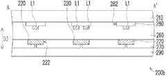
图1A为本发明的第一实施例的一触控显示面板10的剖面示意图。请参考图1A,本实施例的触控显示面板10包括一主动元件阵列基板100、一触控基板200a以及一显示介质300,其中显示介质300配置于主动元件阵列基板100与触控基板200a之间。本实施例的触控基板200a包括一第一基板210、多个第一感测电极220、多个第二感测电极240a、一介电层260以及一黑矩阵280。其中,第一基板210例如是玻璃基板、强化玻璃基板、石英基板、塑胶基板、可挠式软性基板或是上述的复合基板等等。黑矩阵280的材质例如是黑色树脂、铬氧化物、钛氧化物等或是其迭层,且较佳是低反射的材质所构成,在黑矩阵280与第一基板210之间更可以加入其他低反射或是抗反射的材质,例如是多层膜抗反射材料。显示介质300例如是非自发光材料、自发光有机材料、自发光无机材料或上述材料的组合。本发明的显示介质300包含液晶材料、电泳显示材料、有机发光二极管材料、无机发光二极管材料、荧光材料、磷光材料、等离子体材料等,甚至是呈真空状态而于画素结构中涂布荧光物质。本发明的显示介质300以非自发光的液晶材料为范例进行说明,而其他实施例亦可作等效的变化。据此所形成的触控式显示面板可为一液晶显示面板,其例如是穿透式显示面板、反射式显示面板、半穿透半反射式显示面板、微反射型显示面板、垂直配向型(VA)显示面板、水平切换型(IPS)显示面板、多域垂直配向型(MVA)显示面板、扭曲向列型(TN)显示面板、超扭曲向列型(STN)显示面板、图案垂直配向型(PVA)显示面板、超级图案垂直配向型(S-PVA)显示面板、先进大视角型(ASV)显示面板、边缘电场切换型(FFS)显示面板、连续焰火状排列型(CPA)显示面板、轴对称排列微胞型(ASM)显示面板、光学补偿弯曲排列型(OCB)显示面板、超级水平切换型(S-IPS)显示面板、先进超级水平切换型(AS-IPS)显示面板、极端边缘电场切换型(UFFS)显示面板、高分子稳定配向型显示面板、双视角型(dual-view)显示面板、三视角型(triple-view)显示面板、三维立体显示面板(three-dimensional)、多面显示面板(multi-panel)、或其它型面板)、微胶囊型电泳式(micro-capsuleelectrophoretic)显示面板、微罩杯型电泳式(micro-cup electrophoretic)显示面板、向上发光型有机/无机发光二极管显示面板(top emission OLED/LEDdisplay panel)、向下发光型有机/无机发光二极管显示面板(bottom emissionOLED/LED display panel)、双面发光型有机/无机二极管显示面板(dualemission OLED/LED display panel)、等离子体显示面板(PDP)或者是场发射显示面板(FED)等显示装置。详细的材质与结构为本领域通常知识者所熟知,因此不再赘述。FIG. 1A is a schematic cross-sectional view of a
图1B为图1A的触控显示面板10中主动元件阵列基板100以及触控基板200a的配置关系示意图。在此说明的是,图1A是绘示沿图1B中的剖线A-A’的剖面示意图。为了更清楚本实施例的触控基板200a的结构,另以图1C绘示沿图1B中的剖线B-B’的剖面示意图。请同时参考图1A、图1B以及图1C,主动元件阵列基板100包括一第二基板110、多条扫描线120、多条数据线130以及多个画素电极140。扫描线120配置于第二基板110上且沿一第一方向D1延伸。数据线130配置于第二基板110上且沿一第二方向D2延伸,其中扫描线120与数据线130交错布置。画素电极140配置于第二基板110上。须注意的是,图1B中为了清楚绘示第一感测电极220以及第二感测电极240a与主动元件阵列基板100的配置关系,因而省略绘示第一基板210、介电层260、黑矩阵280以及第二基板110。在本实施例中,第一感测电极220是以平行的方式设置于第一基板210上,并且位于第一基板210与主动元件阵列基板100之间,其中各第一感测电极220分别具有多个第一开口222。此外,第一感测电极220沿着第二方向D2延伸,且第一感测电极220与数据线130在一垂直方向D3上约略重叠。第一感测电极220的材质例如是金属、透明导电物质或其他适合的导电物质。其中,金属例如是铝、铜、银、金、钛、钼、钨、铬等,以及其合金或迭层。透明导电物质例如是铟锡氧化物、铟锌氧化物、铝锌氧化物等,以及其混合物或是迭层。FIG. 1B is a schematic diagram of the arrangement relationship between the active
第二感测电极240a是以平行的方式设置在第一基板210上,并且位于第一基板210与主动元件阵列基板100之间,其中第二感测电极240a具有多个第二开口242。此外,第二感测电极240a沿着第一方向D1延伸而与第一感测电极220交错配置且电性绝缘。第二感测电极240a与扫描线120在垂直方向D3上约略重叠。第二感测电极240a的材质例如是金属、透明导电物质或其他适合的导电物质。在本实施例中,第一感测电极220与第二感测电极240a例如是分属不同材料层。换言之,第一感测电极220与第二感测电极240a位于不同平面上。The
此外,每一个第一感测电极220具有多个第一感测区块M1,而每一个第二感测电极240a具有多个第二感测区块M2,其中第一感测区块M1是指第一感测电极220中与第二感测电极240a交错的区域,而第二感测区块M2是指第二感测电极240a中不与第一感测电极220交错的区域。因此,第一感测区块M1与第二感测区块M2在垂直方向D3上不重叠。In addition, each
介电层260例如是全面性地配置于第一感测电极220与第二感测电极240a的之间,而使得第一感测电极220与第二感测电极240a彼此电性绝缘。然,本发明不限于此,在其他实施例中(未绘示),介电层260例如是仅配置于第一感测电极220与第二感测电极240a的交错之处。其中,介电层260的材质可以是无机介电材质、有机介电材质或是其迭层,无机介电材质例如是硅氧化物、硅氮化物、硅氮氧化物、硅碳化物、硅碳氧化物等,有机介电材质例如是聚亚酰胺(polyimide)或压克力树脂等。介电层260的厚度可以是0.1至10微米。The
黑矩阵280配置于第一感测电极220与第一基板210之间,并且配置于第二感测电极240a与第一基板210之间。黑矩阵280具有多个阵列排列的画素开口282,其中各第一开口222分别对应其中一个画素开口282,且各第二开口242分别对应其中一个画素开口282。也就是说,由于第一开口222以及第二开口242对应画素开口282设置,因此光线不会被第一感测电极220以及第二感测电极240a所遮蔽,因此,触控显示面板10可以维持一定的亮度。The
详细而言,各画素开口282的尺寸小于或实质上等于各第一开口222的尺寸,且各画素开口282的尺寸小于或实质上等于各第二开口242的尺寸,其中各第一开口222的尺寸实质上等于各第二开口242的尺寸。换言之,由于黑矩阵280中的画素开口282尺寸小于或实质上等于各第一开口222以及各第二开口242的尺寸,因此黑矩阵280的布线面积大于第一感测电极220以及第二感测电极240a的布线面积。此外,主动元件阵列基板100中的各画素电极140也分别对应于其中一个画素开口282,而且各画素电极140分别与对应的扫描线120以及对应的数据线130电性连接。如此一来,当触控显示面板10运作之时,第一感测电极220以及第二感测电极240a在垂直方向D3上会被黑矩阵280完全覆盖,因此第一感测电极220以及第二感测电极240a的设置就不会影响开口率的大小。Specifically, the size of each
接着,本实施例的触控基板200a可以更包括多个彩色滤光薄膜270以及一平坦层290,其中彩色滤光薄膜270可配置于第一基板210上,且第二感测电极240a可位于介电层260以及彩色滤光薄膜270之间。其中,彩色滤光薄膜270可以是各原色的区块,例如是蓝、绿、红等滤光薄膜区块等,各个彩色滤光薄膜270分别对应于画素开口282配置。平坦层290亦可配置于第一基板210之上,且彩色滤光薄膜270可位于介电层260以及平坦层290之间。其中,彩色滤光薄膜270的厚度例如可以是1至10微米,平坦层290的材质可以使用聚亚酰胺(Polyimide)或压克力树脂(acrylic resin)等有机材质,其厚度可以是1至200微米,且较佳是2至10微米,以减少第一感测电极220以及第二感测电极240a对显示介质300的电性耦合与干扰。Next, the
以下将列举其他实施例以作为说明。在此必须说明的是,下述实施例沿用前述实施例的元件标号与部分内容,其中采用相同的标号来表示相同或近似的元件,并且省略了相同技术内容的说明。此外,为了详细说明本发明的技术特征,以下实施例中仅针对触控基板的部分作说明,而省略了显示介质以及主动元件阵列基板的相关说明。关于省略部分的说明可参考前述实施例,下述实施例不再重复描述。Other embodiments are listed below for illustration. It must be noted here that the following embodiments use the component numbers and part of the content of the previous embodiments, wherein the same numbers are used to denote the same or similar components, and descriptions of the same technical content are omitted. In addition, in order to describe the technical features of the present invention in detail, the following embodiments only describe the part of the touch substrate, and omit the relevant descriptions of the display medium and the active element array substrate. For the description of omitted parts, reference may be made to the foregoing embodiments, and the following embodiments will not be described repeatedly.
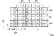
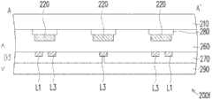
图2A绘示本发明第二实施例的一触控显示面板的一触控基板200b的结构示意图。图2B为沿图2A中剖线A-A’的剖面示意图。图2C为沿2A中剖线B-B’的剖面示意图。须注意的是,图2A仅绘示第一感测电极220以及第二感测电极240b而省略绘示其他构件。请同时参考图2A、图2B以及图2C,于此实施例中,触控基板200b与图1B的触控基板200a的结构相似,惟二者主要差异之处:第二感测电极240b为部分连续性的条状电极。详细而言,第一感测电极220为一具有第一开口222的条状电极。第二感测电极240b则包括多个具有第二开口242的感测垫244以及多条连结于相邻感测垫244之间的第一桥接线L1,第一感测电极220与第一桥接线L1交错,且第一桥接线L1例如是与单一个第一感测电极220交错。在本实施例中,感测垫244与第一桥接线L1例如是属于同一材料层,而第一感测电极220与第二感测电极240b例如是分属不同材料层。换言之,第一感测电极220与第二感测电极240b位于不同平面上,且第二感测电极240b中的各感测垫244则是与第一桥接线L1同时制作且通过第一桥接线L1电性连接各感测垫244。第一感测电极220与第二感测电极240b较佳为条状电极,可以增进制程上的精准度,使第一感测电极220与第二感测电极240b跟黑矩阵280的对准裕度(process window)提高,以避免影响开口率的大小。FIG. 2A is a schematic structural diagram of a
再者,第一桥接线L1的位置对应于黑矩阵280的位置设置,且各第一桥接线L1的宽度小于或实质上等于黑矩阵280的宽度,因此第一桥接线L1可以被黑矩阵280完全地覆盖,以避免影响开口率的大小。Furthermore, the position of the first bridge line L1 is set corresponding to the position of the
另外,在本实施例中,第一感测区块M1是指第一感测电极220中与第二感测电极240b交错的区域,而第二感测区块M2是指第二感测电极240b中感测垫244所位于的区域,其中第一感测区块M1与第二感测区块M2在垂直方向D3上不重叠。In addition, in this embodiment, the first sensing area M1 refers to the area intersecting with the
具体而言,第二感测电极240b是通过第一桥接线L1横跨第一感测电极220以连接相邻的感测垫244,因此第一感测电极220与第二感测电极240b之间的重叠面积仅剩下第一桥接线L1与第一感测电极220之间的重叠面积。如此一来,第一感测电极220与第二感测电极240b之间的重叠面积减少,可使电性干扰的现象获得改善并直接降低第一感测电极与第二感测电极的感应电容。Specifically, the
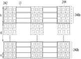
特别一提的是,在本实施例中,第二感测电极240b为紧邻配置。然而,本发明不限于此。于其他实施例中,各第二感测电极240b之间的一间隔距离d可例如是如图2D所示的一个画素单元长度a的非整数倍,或者例如是如图2E所示的一个画素单元长度a的整数倍。另外,第二感测电极240b的宽度h可以是画素单元长度a的非整数倍,例如为图2D所示的2.5倍,或是第二感测电极240b的宽度h可以是画素单元长度a的整数倍,例如为图2E所示的3倍。此外,第一桥接线L1的数目并无限制,只要第一桥接线L1可以被黑矩阵280所遮盖,即为本发明保护的范围。具体而言,本发明中第二感测电极240b之间之间隔距离d的大小、第二感测电极240b的宽度h以及第一桥接线L1的数目可视设计者的实际需求而做线宽线距的调整,以符合理想的感应电容值设计,本发明不以此为限。In particular, in this embodiment, the
图3A绘示本发明第三实施例中触控显示面板的触控基板200c的结构示意图。图3B为沿图3A中剖线A-A’的剖面示意图。图3C为沿图3A中剖线B-B’的剖面示意图。须注意的是,图3A仅绘示第一感测电极220以及第二感测电极240c而省略绘示其他构件。请同时参考图3A、图3B以及图3C,于此实施例中,触控基板200c与图2A的触控基板200b的结构相似,惟二者主要差异之处:在本实施例中,感测垫244与第一桥接线L1例如是属于不同材料层,而第一感测电极220与第二感测电极240c例如是属于同一材料层。详细而言,第一感测电极220与第二感测电极240c中的感测垫244是同时制作且位于同一平面上。各第一桥接线L1是与单一个第一感测电极220交错,并且电性连接相邻的感测垫244。换言之,第二感测电极240c是通过第一桥接线L1横跨第一感测电极220以电性连接相邻的感测垫244,因此,与图2A类似地,第一感测电极220仅与第一桥接线L1于垂直方向D3上重叠。FIG. 3A is a schematic structural diagram of a touch substrate 200c of a touch display panel in a third embodiment of the present invention. Fig. 3B is a schematic cross-sectional view along line A-A' in Fig. 3A. Fig. 3C is a schematic cross-sectional view along the line B-B' in Fig. 3A. It should be noted that FIG. 3A only shows the
图4A绘示本发明第四实施例中触控显示面板的触控基板200d的结构示意图。图4B为沿图4A中剖线A-A’的剖面示意图。图4C为沿图4A中剖线B-B’的剖面示意图。须注意的是,图4A仅绘示第一感测电极220以及第二感测电极240d而省略绘示其他构件。请同时参考图4A、图4B以及图4C,于此实施例中,触控基板200d与图2A的触控基板200b的结构相似,惟二者主要差异之处:本实施例的触控基板200d更包括多个第一接地电极G1以及多个第二接地电极G2。须说明的是,第一接地电极G1与第一感测电极220属于同一材料层,而第二接地电极G2与第二感测电极240d属于同一材料层。详细而言,各第一接地电极G1别分位于相邻的第一感测电极220之间,而各第二接地电极G2分别位于相邻的第二感测电极240d,其中各第一桥接线L1是与多个第一感测电极220以及其中一个第一接地电极G1交错。此外,各第二感测电极240d中与第一接地电极G1重叠之处并不属于感测垫244的区域。具体而言,由于第一接地电极G1与第二接地电极G2会用以接地,而与第一感测电极220以及第二感测电极240d的电压不同,因此第一接地电极G1可以用来屏蔽相邻的第一感测电极220,而第二接地电极可以用来屏蔽相邻的第二感测电极240b,以减少电性干扰的现象。FIG. 4A is a schematic structural diagram of a
图5A绘示本发明第五实施例中触控显示面板的触控基板200e的结构示意图。图5B为沿图5A中剖线A-A’的剖面示意图。图5C为沿图5A中剖线B-B’的剖面示意图。须注意的是,图5A仅绘示第一感测电极220以及第二感测电极240e而省略绘示其他构件。请同时参考图5A、图5B以及图5C,于此实施例中,触控基板200e与图4A的触控基板200d的结构相似,惟二者主要差异之处:本实施例的感测垫244与第一桥接线L1例如是属于不同材料层,而第一感测电极220与第二感测电极240e例如是属于同一材料层。此外,本实施例的触控基板200e更包括多条第二桥接线L2,且第二桥接线L2与第一感测电极220交错。具体而言,触控基板200e中的第一接地电极G1可以屏蔽各第一感测电极220之间的电性干扰,而第二接地电极G2可以屏蔽各第二感测电极240e之间的电性干扰。此外,相邻的感测垫244是通过位于不同平面的第一桥接线L1电性连接,而第一接地电极G1与第二接地电极G2是通过第二桥接线L2电性连接。FIG. 5A is a schematic structural diagram of a
图6A绘示本发明第六实施例中触控显示面板的触控基板200f的结构示意图。图6B为沿图6A中剖线A-A’的剖面示意图。图6C为沿图6A中剖线B-B’的剖面示意图。须注意的是,图6A仅绘示第一感测电极220以及第二感测电极240f而省略绘示其他构件。请同时参考图6A、图6B以及图6C,于此实施例中,触控基板200f包括多个接地电极G,各接地电极G分别位于相邻的感测垫244之间以及感测垫244与第一感测电极220之间。因此接地电极G可以减少各感测垫244之间的电性干扰,而且接地电极G可以减少感测垫244与第一感测电极220之间的电性干扰。此外,接地电极G与第一感测电极220以及第二感测电极240f是属于同一材料层,即位于同一平面上。另外,接地电极G之间通过多条第三桥接线L3彼此电性连接,而感测垫244彼此之间是通过第一桥接线L1电性连接。FIG. 6A is a schematic structural diagram of a
本发明的触控显示面板可以对照上述的结构,使用沉积、微影与蚀刻等制程,依照层别依序制作而成,其详细的制造步骤可以对照上述的结构,此皆为本领域通常知识者所熟知,因此不再赘述。本发明的触控显示面板可以使用互感式(mutual-type)电容感测方式驱动侦测,例如是以第一感测电极220为驱动电极,第二感测电极240a为侦测电极,利用电容变化判断出触碰触控面板的导体(例如是手指)的位置。另外亦可第一感测电极220为侦测电极,第二感测电极240a为驱动电极,亦可达到近似的效果。此外,也可以使用自感式(self-type)电容感测方式驱动侦测,对第一感测电极220与第二感测电极240a分别施加独立的驱动感测信号,利用电容变化判断出触碰触控面板的导体(例如是手指)的位置。至于详细的驱动方法,此皆为本领域通常知识者所熟知,因此不再赘述。The touch display panel of the present invention can be fabricated in accordance with the above-mentioned structure by using processes such as deposition, lithography, and etching in sequence, and its detailed manufacturing steps can be compared with the above-mentioned structure, which is common knowledge in the art are well known, so no further details are given. The touch display panel of the present invention can be driven and detected using a mutual-type capacitance sensing method. The change determines the position of the conductor (such as a finger) touching the touch panel. In addition, the
综上所述,通过具有开口、桥接线及/或接地电极的设计的感测电极以形成触控基板的主要构件,可以减少触控基板的构件之间发生串音的现象。此外,上述开口是对应画素开口而设置,因此本发明的触控显示面板不会因为感测电极的设置而影响其亮度。再者,感测电极的布线是对应黑矩阵而设置,因此从观赏者的角度看来,黑矩阵的面积会完全覆盖感测电极的面积。换言的,感测电极的设置不会影响开口率的大小。如此一来,触控基板的设置将不会影响画面的显示。从另一方面来看,本发明的用于内建式的触控显示面板是由具有开口的感测电极全面性的交错布置于基板上,因此感测电极更可以当作是现有的遮蔽层,以用来减少触控单元运作时,被用以触碰触控面板的导体(例如是手指)干扰的可能性。换言之,本发明的触控显示面板进一步整合了遮蔽层的功能,而不需要另外制作遮蔽层。如此一来,具有此触控基板的触控显示面板可具有较佳的信号灵敏度。To sum up, the main components of the touch substrate are formed by designing the sensing electrodes with openings, bridge lines and/or ground electrodes, which can reduce crosstalk between components of the touch substrate. In addition, the above-mentioned openings are set corresponding to the pixel openings, so the brightness of the touch display panel of the present invention will not be affected by the arrangement of the sensing electrodes. Furthermore, the wiring of the sensing electrodes is arranged corresponding to the black matrix, so from the viewer's point of view, the area of the black matrix will completely cover the area of the sensing electrodes. In other words, the arrangement of the sensing electrodes will not affect the size of the aperture ratio. In this way, the setting of the touch substrate will not affect the display of the screen. From another point of view, the built-in touch display panel of the present invention has sensing electrodes with openings that are comprehensively and staggeredly arranged on the substrate, so the sensing electrodes can be regarded as existing shielding The layer is used to reduce the possibility of interference from conductors (such as fingers) used to touch the touch panel when the touch unit is in operation. In other words, the touch display panel of the present invention further integrates the function of the shielding layer without additionally making a shielding layer. In this way, the touch display panel with the touch substrate can have better signal sensitivity.
虽然本发明已以实施例揭露如上,然其并非用以限定本发明,任何所属技术领域中具有通常知识者,在不脱离本发明的精神和范围内,当可作些许的更动与润饰,故本发明的保护范围当视后附的申请专利范围所界定者为准。Although the present invention has been disclosed as above with the embodiments, it is not intended to limit the present invention. Anyone with ordinary knowledge in the technical field can make some changes and modifications without departing from the spirit and scope of the present invention. Therefore, the scope of protection of the present invention should be defined by the scope of the appended patent application.
Claims (19)
Applications Claiming Priority (2)
| Application Number | Priority Date | Filing Date | Title |
|---|---|---|---|
| TW100145313ATWI456321B (en) | 2011-12-08 | 2011-12-08 | Touch display panel |
| TW100145313 | 2011-12-08 |
Publications (2)
| Publication Number | Publication Date |
|---|---|
| CN102541355Atrue CN102541355A (en) | 2012-07-04 |
| CN102541355B CN102541355B (en) | 2014-09-17 |
Family
ID=46348378
Family Applications (1)
| Application Number | Title | Priority Date | Filing Date |
|---|---|---|---|
| CN201210063491.5AActiveCN102541355B (en) | 2011-12-08 | 2012-03-12 | Touch control display panel |
Country Status (3)
| Country | Link |
|---|---|
| US (1) | US9007337B2 (en) |
| CN (1) | CN102541355B (en) |
| TW (1) | TWI456321B (en) |
Cited By (25)
| Publication number | Priority date | Publication date | Assignee | Title |
|---|---|---|---|---|
| CN103064573A (en)* | 2013-01-11 | 2013-04-24 | 北京京东方光电科技有限公司 | Capacitive touch screen |
| CN103279251A (en)* | 2013-04-24 | 2013-09-04 | 友达光电股份有限公司 | Touch panel |
| CN103472965A (en)* | 2013-09-13 | 2013-12-25 | 北京京东方光电科技有限公司 | Array substrate and touch display device |
| CN103677399A (en)* | 2012-09-11 | 2014-03-26 | 三星显示有限公司 | Sensor substrate, manufacturing method thereof, and sensing display panel having same |
| CN103677465A (en)* | 2012-09-19 | 2014-03-26 | 上海天马微电子有限公司 | Capacitive touch panel and display |
| CN103853377A (en)* | 2012-11-30 | 2014-06-11 | 株式会社日本显示器 | Display device with touch detection function and electronic apparatus |
| CN103913871A (en)* | 2012-12-28 | 2014-07-09 | 业鑫科技顾问股份有限公司 | touch display device |
| CN103913869A (en)* | 2012-12-31 | 2014-07-09 | 上海天马微电子有限公司 | Liquid crystal display with embedded touch device and forming method thereof |
| CN104182075A (en)* | 2013-05-28 | 2014-12-03 | 三星显示有限公司 | Display device |
| CN104516168A (en)* | 2012-11-21 | 2015-04-15 | 京东方科技集团股份有限公司 | Convertible lens and preparation method thereof, as well as two-dimension and three-dimension display baseplate and display device |
| CN104750342A (en)* | 2013-12-26 | 2015-07-01 | 乐金显示有限公司 | Touch screen panel and method of manufacturing the same |
| CN105183220A (en)* | 2015-07-02 | 2015-12-23 | 友达光电股份有限公司 | Touch display device and driving method thereof |
| CN105549780A (en)* | 2015-10-02 | 2016-05-04 | 友达光电股份有限公司 | Touch panel and manufacturing method thereof |
| CN105705989A (en)* | 2013-11-11 | 2016-06-22 | 凸版印刷株式会社 | Liquid crystal display device |
| WO2016145773A1 (en)* | 2015-03-16 | 2016-09-22 | 京东方科技集团股份有限公司 | Color film substrate, touch display screen and method for manufacturing color film substrate |
| CN106062618A (en)* | 2014-02-28 | 2016-10-26 | 凸版印刷株式会社 | Liquid crystal display device |
| CN106201043A (en)* | 2015-05-08 | 2016-12-07 | 群创光电股份有限公司 | Touch control structure and application thereof |
| CN106354322A (en)* | 2016-05-31 | 2017-01-25 | 友达光电股份有限公司 | Touch panel |
| CN106371667A (en)* | 2016-06-27 | 2017-02-01 | 友达光电股份有限公司 | Panel board |
| CN106445261A (en)* | 2015-08-07 | 2017-02-22 | 群创光电股份有限公司 | Touch display device |
| CN106598321A (en)* | 2015-10-16 | 2017-04-26 | 群创光电股份有限公司 | Touch display panel and pixel structure |
| CN107065267A (en)* | 2017-05-22 | 2017-08-18 | 东旭(昆山)显示材料有限公司 | Touch screen color membrane substrates |
| CN107634085A (en)* | 2017-09-15 | 2018-01-26 | 业成科技(成都)有限公司 | Touch control display apparatus and its manufacture method |
| CN109766032A (en)* | 2014-10-22 | 2019-05-17 | 赛普拉斯半导体公司 | Low-power capacitance type sensor button |
| CN112639697A (en)* | 2018-09-03 | 2021-04-09 | 深圳市柔宇科技股份有限公司 | Touch display panel and touch display device |
Families Citing this family (49)
| Publication number | Priority date | Publication date | Assignee | Title |
|---|---|---|---|---|
| JPWO2014045602A1 (en)* | 2012-09-24 | 2016-08-18 | パナソニックIpマネジメント株式会社 | Display device |
| TWI509335B (en)* | 2012-10-05 | 2015-11-21 | Innocom Tech Shenzhen Co Ltd | Tft touch-control display panel device and driving method thereof |
| CN102981343B (en)* | 2012-11-21 | 2015-01-07 | 京东方科技集团股份有限公司 | Conversion lens and its preparation method, two-dimensional-three-dimensional display substrate and display device |
| US20140225859A1 (en)* | 2013-02-14 | 2014-08-14 | Broadcom Corporation | Mutual capacitive touch sensor pattern |
| TWI531844B (en)* | 2013-03-04 | 2016-05-01 | 聯詠科技股份有限公司 | Capacitive touch panel and controlling method thereof |
| CN103207719A (en)* | 2013-03-28 | 2013-07-17 | 北京京东方光电科技有限公司 | Capacitive inlaid touch screen and display device |
| CN103186287B (en)* | 2013-03-28 | 2015-12-23 | 合肥京东方光电科技有限公司 | A kind of touching display screen and touch control display apparatus |
| KR102050446B1 (en)* | 2013-06-26 | 2019-12-02 | 엘지디스플레이 주식회사 | Diode display device including touch panel |
| TWI485599B (en)* | 2013-08-15 | 2015-05-21 | Hannstouch Solution Inc | Touch component and flat panel display |
| CN104461182B (en)* | 2013-09-16 | 2017-07-28 | 和鑫光电股份有限公司 | Touch element and flat display device |
| CN103488341A (en)* | 2013-09-23 | 2014-01-01 | 京东方科技集团股份有限公司 | In-cell touch panel and display device |
| KR102116483B1 (en) | 2013-10-18 | 2020-05-29 | 삼성디스플레이 주식회사 | Touch screen panel and fabrication method of the same |
| CN103558942B (en)* | 2013-11-08 | 2016-03-09 | 京东方科技集团股份有限公司 | Touch-screen and manufacture method thereof |
| KR102239367B1 (en) | 2013-11-27 | 2021-04-09 | 가부시키가이샤 한도오따이 에네루기 켄큐쇼 | Touch panel |
| KR102192035B1 (en)* | 2013-12-02 | 2020-12-17 | 삼성디스플레이 주식회사 | Flexible display device including touch detecting sensor |
| KR20150073539A (en)* | 2013-12-23 | 2015-07-01 | 삼성전자주식회사 | Apparatus and method for sensing a touch input in electronic device |
| CN103792711A (en)* | 2014-01-14 | 2014-05-14 | 京东方科技集团股份有限公司 | Touch display panel and manufacturing method thereof |
| CN103941952B (en)* | 2014-03-31 | 2017-03-29 | 上海天马微电子有限公司 | Electromagnetic induction type touch substrate and inductive touch display device |
| TWI518434B (en)* | 2014-04-25 | 2016-01-21 | 元太科技工業股份有限公司 | Display device |
| US9836165B2 (en)* | 2014-05-16 | 2017-12-05 | Apple Inc. | Integrated silicon-OLED display and touch sensor panel |
| CN104020913A (en)* | 2014-05-30 | 2014-09-03 | 京东方科技集团股份有限公司 | Embedded touch screen and display device |
| TWI765679B (en) | 2014-05-30 | 2022-05-21 | 日商半導體能源研究所股份有限公司 | Touch panel |
| WO2016006081A1 (en)* | 2014-07-10 | 2016-01-14 | 凸版印刷株式会社 | Black electrode substrate, production method for black electrode substrate, and display device |
| US20160124548A1 (en)* | 2014-11-03 | 2016-05-05 | Northwestern University | Materials and structures for haptic displays with simultaneous sensing and actuation |
| CN104375707A (en)* | 2014-11-21 | 2015-02-25 | 重庆京东方光电科技有限公司 | Touch display panel and touch display device |
| CN104393025B (en)* | 2014-12-09 | 2017-08-11 | 京东方科技集团股份有限公司 | A kind of array base palte, touch-control display panel and touch control display apparatus |
| CN104777684B (en)* | 2015-04-24 | 2018-06-01 | 京东方科技集团股份有限公司 | Self-capacitance touch liquid crystal grating and preparation method thereof, display screen, display device |
| CN105093616B (en)* | 2015-08-04 | 2018-10-26 | 深圳市华星光电技术有限公司 | VA type In-cell touch display panel structures |
| CN106896951B (en) | 2015-10-07 | 2019-11-29 | 财团法人工业技术研究院 | Touch display panel |
| TWI552052B (en)* | 2015-11-10 | 2016-10-01 | 奇景光電股份有限公司 | In-cell touch display panel |
| KR102412369B1 (en)* | 2015-11-16 | 2022-06-24 | 주식회사 지2터치 | Display device integrated with touch screen |
| CN110580114B (en)* | 2015-11-20 | 2023-04-21 | 奇景光电股份有限公司 | Embedded touch display panel |
| JP6175698B1 (en)* | 2015-12-28 | 2017-08-09 | 凸版印刷株式会社 | Liquid crystal display |
| CN105652496B (en)* | 2016-01-25 | 2018-03-09 | 武汉华星光电技术有限公司 | A kind of array base palte and touch-screen |
| KR102562896B1 (en)* | 2016-03-18 | 2023-08-04 | 삼성디스플레이 주식회사 | Display apparatus |
| KR102562627B1 (en) | 2016-03-21 | 2023-08-03 | 삼성디스플레이 주식회사 | Display device |
| CN106201074B (en)* | 2016-06-30 | 2019-08-09 | 京东方科技集团股份有限公司 | Touch substrate, manufacturing method thereof, and touch screen |
| TWI579750B (en)* | 2016-07-01 | 2017-04-21 | 友達光電股份有限公司 | Touch panel and method for manufacturing the same |
| US10541280B1 (en) | 2016-09-16 | 2020-01-21 | Apple Inc. | OLED based touch sensing and user identification |
| KR102567934B1 (en) | 2016-09-30 | 2023-08-18 | 엘지디스플레이 주식회사 | Organic light emitting display and touch senising method for the same |
| KR102276074B1 (en)* | 2017-03-17 | 2021-07-12 | 도레이 카부시키가이샤 | Method for manufacturing a substrate with a wiring electrode and a substrate with a wiring electrode |
| CN107783699B (en)* | 2017-10-16 | 2021-05-04 | 业成科技(成都)有限公司 | Touch panel structure and manufacturing method thereof |
| KR102508978B1 (en) | 2017-11-09 | 2023-03-13 | 삼성디스플레이 주식회사 | Sensing unit and display device having the same |
| CN109240004A (en)* | 2018-10-08 | 2019-01-18 | 深圳市华星光电半导体显示技术有限公司 | Improve the method and device of display contrast |
| CN112002278B (en)* | 2020-08-28 | 2022-07-15 | 合肥维信诺科技有限公司 | Display panel and debugging method thereof |
| CN114461089A (en)* | 2020-11-10 | 2022-05-10 | 合肥鑫晟光电科技有限公司 | Touch pad, touch display device and preparation method thereof |
| TWI757036B (en)* | 2021-01-06 | 2022-03-01 | 友達光電股份有限公司 | Touch display panel |
| KR20230093835A (en)* | 2021-12-20 | 2023-06-27 | 엘지디스플레이 주식회사 | Transparent display device with touch sensor |
| CN117472224A (en)* | 2023-10-18 | 2024-01-30 | 厦门天马显示科技有限公司 | Display panels and display devices |
Citations (4)
| Publication number | Priority date | Publication date | Assignee | Title |
|---|---|---|---|---|
| CN101261392A (en)* | 2008-04-17 | 2008-09-10 | 友达光电股份有限公司 | Touch display panel, color filter substrate and manufacturing method thereof |
| US20090102814A1 (en)* | 2007-10-19 | 2009-04-23 | Tpo Displays Corp. | Image displaying systems |
| CN101441537A (en)* | 2008-12-18 | 2009-05-27 | 友达光电股份有限公司 | Touch control display panel |
| CN101738772A (en)* | 2009-12-16 | 2010-06-16 | 深超光电(深圳)有限公司 | Touch display device |
Family Cites Families (10)
| Publication number | Priority date | Publication date | Assignee | Title |
|---|---|---|---|---|
| US7932898B2 (en)* | 2005-09-20 | 2011-04-26 | Atmel Corporation | Touch sensitive screen |
| US8040321B2 (en) | 2006-07-10 | 2011-10-18 | Cypress Semiconductor Corporation | Touch-sensor with shared capacitive sensors |
| US20080309633A1 (en) | 2007-06-13 | 2008-12-18 | Apple Inc. | Touch-sensitive display |
| US20090194344A1 (en) | 2008-01-31 | 2009-08-06 | Avago Technologies Ecbu Ip (Singapore) Pte. Ltd. | Single Layer Mutual Capacitance Sensing Systems, Device, Components and Methods |
| TWI380089B (en)* | 2008-12-03 | 2012-12-21 | Au Optronics Corp | Method of forming a color filter touch sensing substrate |
| CN101424817B (en) | 2008-12-17 | 2010-07-21 | 友达光电股份有限公司 | Method for manufacturing color filtering touch substrate |
| CN101441347B (en) | 2008-12-23 | 2010-09-01 | 友达光电股份有限公司 | Color filtering touch substrate, display panel and manufacturing method of color filtering touch substrate and display panel |
| US7995041B2 (en) | 2009-02-02 | 2011-08-09 | Apple Inc. | Integrated touch screen |
| CN101819344A (en) | 2010-05-20 | 2010-09-01 | 友达光电股份有限公司 | Color filter touch substrate |
| KR101230196B1 (en)* | 2010-10-29 | 2013-02-06 | 삼성디스플레이 주식회사 | Liquid Crystal Display having a Touch Screen Panel |
- 2011
- 2011-12-08TWTW100145313Apatent/TWI456321B/enactive
- 2012
- 2012-03-12CNCN201210063491.5Apatent/CN102541355B/enactiveActive
- 2012-09-14USUS13/615,680patent/US9007337B2/enactiveActive
Patent Citations (4)
| Publication number | Priority date | Publication date | Assignee | Title |
|---|---|---|---|---|
| US20090102814A1 (en)* | 2007-10-19 | 2009-04-23 | Tpo Displays Corp. | Image displaying systems |
| CN101261392A (en)* | 2008-04-17 | 2008-09-10 | 友达光电股份有限公司 | Touch display panel, color filter substrate and manufacturing method thereof |
| CN101441537A (en)* | 2008-12-18 | 2009-05-27 | 友达光电股份有限公司 | Touch control display panel |
| CN101738772A (en)* | 2009-12-16 | 2010-06-16 | 深超光电(深圳)有限公司 | Touch display device |
Cited By (56)
| Publication number | Priority date | Publication date | Assignee | Title |
|---|---|---|---|---|
| CN103677399A (en)* | 2012-09-11 | 2014-03-26 | 三星显示有限公司 | Sensor substrate, manufacturing method thereof, and sensing display panel having same |
| CN103677399B (en)* | 2012-09-11 | 2019-05-10 | 三星显示有限公司 | Sensor substrate, manufacturing method thereof, and sensing display panel having the same |
| CN103677465B (en)* | 2012-09-19 | 2017-02-22 | 上海天马微电子有限公司 | Capacitive touch panel and display |
| CN103677465A (en)* | 2012-09-19 | 2014-03-26 | 上海天马微电子有限公司 | Capacitive touch panel and display |
| EP2738595A4 (en)* | 2012-09-19 | 2015-05-27 | Shanghai Tianma Micro Elect Co | Embedded capacitive touch panel, display, and manufacturing method |
| CN104516168A (en)* | 2012-11-21 | 2015-04-15 | 京东方科技集团股份有限公司 | Convertible lens and preparation method thereof, as well as two-dimension and three-dimension display baseplate and display device |
| CN104516168B (en)* | 2012-11-21 | 2018-05-08 | 京东方科技集团股份有限公司 | Convertible lens and preparation method thereof, 2 d-3 d display base plate and display device |
| US12111993B2 (en) | 2012-11-30 | 2024-10-08 | Japan Display Inc. | Display device with touch detection function and electronic apparatus |
| CN109062449A (en)* | 2012-11-30 | 2018-12-21 | 株式会社日本显示器 | Display device with touch detection function |
| US10067624B2 (en) | 2012-11-30 | 2018-09-04 | Japan Display Inc. | Display device with touch detection function and electronic apparatus |
| CN103853377A (en)* | 2012-11-30 | 2014-06-11 | 株式会社日本显示器 | Display device with touch detection function and electronic apparatus |
| US11914808B2 (en) | 2012-11-30 | 2024-02-27 | Japan Display Inc. | Display device with a touch detection device |
| CN109062449B (en)* | 2012-11-30 | 2022-06-17 | 株式会社日本显示器 | Display device with touch detection function |
| US9626060B2 (en) | 2012-11-30 | 2017-04-18 | Japan Display Inc. | Display device with touch detection function and electronic apparatus |
| CN103853377B (en)* | 2012-11-30 | 2018-10-19 | 株式会社日本显示器 | Display device and electronic device with touch detection function |
| US11327591B2 (en) | 2012-11-30 | 2022-05-10 | Japan Display Inc. | Display device with touch detection device |
| US10996784B2 (en) | 2012-11-30 | 2021-05-04 | Japan Display Inc. | Display device with touch detection device |
| US10613698B2 (en) | 2012-11-30 | 2020-04-07 | Japan Display Inc. | Display device with touch detection device |
| US10303320B2 (en) | 2012-11-30 | 2019-05-28 | Japan Display Inc. | Display device with touch detection function and electronic apparatus |
| CN103913871A (en)* | 2012-12-28 | 2014-07-09 | 业鑫科技顾问股份有限公司 | touch display device |
| CN103913869A (en)* | 2012-12-31 | 2014-07-09 | 上海天马微电子有限公司 | Liquid crystal display with embedded touch device and forming method thereof |
| CN103064573A (en)* | 2013-01-11 | 2013-04-24 | 北京京东方光电科技有限公司 | Capacitive touch screen |
| CN103279251B (en)* | 2013-04-24 | 2016-08-10 | 友达光电股份有限公司 | Touch panel |
| CN103279251A (en)* | 2013-04-24 | 2013-09-04 | 友达光电股份有限公司 | Touch panel |
| CN104182075A (en)* | 2013-05-28 | 2014-12-03 | 三星显示有限公司 | Display device |
| CN104182075B (en)* | 2013-05-28 | 2018-11-16 | 三星显示有限公司 | Display device |
| CN103472965B (en)* | 2013-09-13 | 2019-02-26 | 北京京东方光电科技有限公司 | A kind of array substrate and touch control display apparatus |
| CN103472965A (en)* | 2013-09-13 | 2013-12-25 | 北京京东方光电科技有限公司 | Array substrate and touch display device |
| CN105705989A (en)* | 2013-11-11 | 2016-06-22 | 凸版印刷株式会社 | Liquid crystal display device |
| CN105705989B (en)* | 2013-11-11 | 2018-11-09 | 凸版印刷株式会社 | Liquid crystal display device |
| US9891764B2 (en) | 2013-12-26 | 2018-02-13 | Lg Display Co., Ltd. | Touch screen panel |
| CN104750342A (en)* | 2013-12-26 | 2015-07-01 | 乐金显示有限公司 | Touch screen panel and method of manufacturing the same |
| CN106062618B (en)* | 2014-02-28 | 2019-04-16 | 凸版印刷株式会社 | Liquid crystal display device |
| CN106062618A (en)* | 2014-02-28 | 2016-10-26 | 凸版印刷株式会社 | Liquid crystal display device |
| CN109766032B (en)* | 2014-10-22 | 2021-02-02 | 赛普拉斯半导体公司 | Low power capacitive sensor button |
| US10558313B2 (en) | 2014-10-22 | 2020-02-11 | Cypress Semiconductor Corporation | Low power capacitive sensor button |
| CN109766032A (en)* | 2014-10-22 | 2019-05-17 | 赛普拉斯半导体公司 | Low-power capacitance type sensor button |
| WO2016145773A1 (en)* | 2015-03-16 | 2016-09-22 | 京东方科技集团股份有限公司 | Color film substrate, touch display screen and method for manufacturing color film substrate |
| CN106201043B (en)* | 2015-05-08 | 2019-10-11 | 群创光电股份有限公司 | Touch control structure and application thereof |
| CN106201043A (en)* | 2015-05-08 | 2016-12-07 | 群创光电股份有限公司 | Touch control structure and application thereof |
| US10146381B2 (en) | 2015-05-08 | 2018-12-04 | Innolux Corporation | Touch sensing structure and applications thereof |
| CN105183220B (en)* | 2015-07-02 | 2018-07-06 | 友达光电股份有限公司 | Touch display device and driving method thereof |
| CN105183220A (en)* | 2015-07-02 | 2015-12-23 | 友达光电股份有限公司 | Touch display device and driving method thereof |
| CN106445261A (en)* | 2015-08-07 | 2017-02-22 | 群创光电股份有限公司 | Touch display device |
| CN105549780B (en)* | 2015-10-02 | 2018-12-25 | 友达光电股份有限公司 | Touch panel and manufacturing method thereof |
| CN105549780A (en)* | 2015-10-02 | 2016-05-04 | 友达光电股份有限公司 | Touch panel and manufacturing method thereof |
| CN106598321A (en)* | 2015-10-16 | 2017-04-26 | 群创光电股份有限公司 | Touch display panel and pixel structure |
| CN106598321B (en)* | 2015-10-16 | 2019-10-18 | 群创光电股份有限公司 | Touch display panel and pixel structure |
| CN106354322B (en)* | 2016-05-31 | 2019-07-23 | 友达光电股份有限公司 | touch panel |
| CN106354322A (en)* | 2016-05-31 | 2017-01-25 | 友达光电股份有限公司 | Touch panel |
| CN106371667B (en)* | 2016-06-27 | 2020-07-10 | 友达光电股份有限公司 | Panel board |
| CN106371667A (en)* | 2016-06-27 | 2017-02-01 | 友达光电股份有限公司 | Panel board |
| CN107065267A (en)* | 2017-05-22 | 2017-08-18 | 东旭(昆山)显示材料有限公司 | Touch screen color membrane substrates |
| CN107634085B (en)* | 2017-09-15 | 2020-11-17 | 业成科技(成都)有限公司 | Touch display device and manufacturing method thereof |
| CN107634085A (en)* | 2017-09-15 | 2018-01-26 | 业成科技(成都)有限公司 | Touch control display apparatus and its manufacture method |
| CN112639697A (en)* | 2018-09-03 | 2021-04-09 | 深圳市柔宇科技股份有限公司 | Touch display panel and touch display device |
Also Published As
| Publication number | Publication date |
|---|---|
| US9007337B2 (en) | 2015-04-14 |
| CN102541355B (en) | 2014-09-17 |
| TW201324003A (en) | 2013-06-16 |
| TWI456321B (en) | 2014-10-11 |
| US20130147730A1 (en) | 2013-06-13 |
Similar Documents
| Publication | Publication Date | Title |
|---|---|---|
| CN102541355B (en) | Touch control display panel | |
| US10452201B1 (en) | Touch sensor for display with shield | |
| US12039128B2 (en) | Touch panel | |
| US10845902B2 (en) | Touch sensor for display | |
| US10473964B2 (en) | Touch display panel and method for manufacturing the same | |
| US8581875B2 (en) | Touch panel, display, and manufacturing method of touch panel | |
| CN101305338B (en) | Display device | |
| CN101872086B (en) | LCD Monitor | |
| US10592028B2 (en) | Touch sensor feedlines for display | |
| US20100328248A1 (en) | Capacitive touch screen with reduced electrode trace resistance | |
| CN101414070B (en) | Touch electrode layer and display panel | |
| US10209841B2 (en) | Position inputting device and display device with position inputting function | |
| JP2008233976A (en) | Touch panel, display device, and method for manufacturing touch panel | |
| CN110262680B (en) | Touch sensor and display device including the same | |
| TW201308176A (en) | Capacitive touch panel and method for reducing visibility of its metal conductor | |
| TW201020890A (en) | Sensing electrode layer and display panel | |
| TWI578214B (en) | Touch panel and manufacturing method thereof | |
| KR20120138288A (en) | Capacitive type touch panel | |
| US9626047B2 (en) | Capacitive touch unit and capacitive touch screen | |
| WO2020224039A1 (en) | Touch panel | |
| KR20140016627A (en) | Touch screen device | |
| JP2013097704A (en) | Display device | |
| JP2019109767A (en) | Detection device and display device |
Legal Events
| Date | Code | Title | Description |
|---|---|---|---|
| C06 | Publication | ||
| PB01 | Publication | ||
| C10 | Entry into substantive examination | ||
| SE01 | Entry into force of request for substantive examination | ||
| C14 | Grant of patent or utility model | ||
| GR01 | Patent grant |