CN102541339A - touch display device - Google Patents
touch display deviceDownload PDFInfo
- Publication number
- CN102541339A CN102541339ACN2010106241291ACN201010624129ACN102541339ACN 102541339 ACN102541339 ACN 102541339ACN 2010106241291 ACN2010106241291 ACN 2010106241291ACN 201010624129 ACN201010624129 ACN 201010624129ACN 102541339 ACN102541339 ACN 102541339A
- Authority
- CN
- China
- Prior art keywords
- shielding electrode
- sensing
- area
- display panel
- those
- Prior art date
- Legal status (The legal status is an assumption and is not a legal conclusion. Google has not performed a legal analysis and makes no representation as to the accuracy of the status listed.)
- Pending
Links
- 239000000758substrateSubstances0.000claimsabstractdescription36
- 239000000463materialSubstances0.000claimsdescription10
- 230000003287optical effectEffects0.000claimsdescription7
- 238000009413insulationMethods0.000claims9
- 239000004568cementSubstances0.000claims1
- 239000010410layerSubstances0.000description79
- 230000003068static effectEffects0.000description5
- 230000000007visual effectEffects0.000description5
- 230000000694effectsEffects0.000description4
- 238000010586diagramMethods0.000description3
- 238000009825accumulationMethods0.000description2
- 239000004020conductorSubstances0.000description2
- 238000005034decorationMethods0.000description2
- 230000005611electricityEffects0.000description2
- 239000003292glueSubstances0.000description2
- 239000011521glassSubstances0.000description1
- 239000011810insulating materialSubstances0.000description1
- 239000002184metalSubstances0.000description1
- 238000000034methodMethods0.000description1
- 238000012986modificationMethods0.000description1
- 230000004048modificationEffects0.000description1
- 230000035515penetrationEffects0.000description1
- 230000000704physical effectEffects0.000description1
- 230000002265preventionEffects0.000description1
- 239000011241protective layerSubstances0.000description1
- 125000006850spacer groupChemical group0.000description1
Images


Landscapes
- Position Input By Displaying (AREA)
Abstract
Description
Translated fromChinese技术领域technical field
本发明涉及一种显示装置,且尤其涉及一种触控显示装置。The present invention relates to a display device, and in particular to a touch display device.
背景技术Background technique
图1示出已知一种电容式触控面板的局部上视示意图。请参照图1,电容式触控面板100包括一第一感测串列120、以及一第二感测串列130,其中第一感测串列120与第二感测串列130分别由多个第一感测电极122与多个第二感测电极132所构成。第一感测电极122与第二感测电极132间维持一定的间距G以产生对应的感测电容而实现触控感测的功能。此外,第一感测串列120与第二感测串列130往往需配置至少一间隔绝缘层(未标示)维持第一感测串列120与第二感测串列130的电性独立。也就是说,间隔绝缘层在间距G所在位置会被暴露出来。FIG. 1 shows a schematic partial top view of a known capacitive touch panel. Please refer to FIG. 1 , the capacitive touch panel 100 includes a first sensing series 120 and a second sensing series 130, wherein the first sensing series 120 and the second sensing series 130 are composed of multiple It is composed of a first sensing electrode 122 and a plurality of second sensing electrodes 132 . A certain distance G is maintained between the first sensing electrode 122 and the second sensing electrode 132 to generate a corresponding sensing capacitance to realize the function of touch sensing. In addition, the first sensing series 120 and the second sensing series 130 often need to configure at least one insulating layer (not marked) to maintain the electrical independence of the first sensing series 120 and the second sensing series 130 . That is to say, the spacer insulating layer will be exposed at the position where the gap G is located.
然而,这样的设计会使电容式触控面板100所提供的视觉效果(visual effect)不甚理想。详言之,光线通过不同材质的界面(interface)时,会发生折射、反射、穿透等物理现象,其中这些物理现象随着材质的特性而有所不同。以电容式触控面板100而言,在位置X处,光线会通过第一感测电极122以及介电层;而在位置Y处,光线会通过第二感测电极132以及介电层;另外,在位置Z处(也就是间距G所在之处),光线则仅通过介电层。感测电极与介电层的折射率等物理性质不同。所以,人眼观看电容式触控面板100时会感受到亮度不均的情形,特别是第一感测电极122与第二感测电极132的轮廓可能被人眼所察觉。However, such a design makes the visual effect provided by the capacitive touch panel 100 unsatisfactory. In detail, when light passes through the interface of different materials, physical phenomena such as refraction, reflection, and penetration will occur, and these physical phenomena are different according to the characteristics of the material. Taking the capacitive touch panel 100 as an example, at the position X, the light will pass through the first sensing electrode 122 and the dielectric layer; at the position Y, the light will pass through the second sensing electrode 132 and the dielectric layer; in addition , at position Z (that is, where the distance G is), the light only passes through the dielectric layer. Physical properties such as the refractive index of the sensing electrode and the dielectric layer are different. Therefore, human eyes may experience uneven brightness when watching the capacitive touch panel 100 , especially the contours of the first sensing electrodes 122 and the second sensing electrodes 132 may be perceived by human eyes.
当电容式触控面板100与显示面板整合时,将对显示面板的显示效果造成负面的影响。此外,电容式触控面板100与显示面板整合时的信号干扰情形更是对显示效果产生不佳的影响。When the capacitive touch panel 100 is integrated with the display panel, it will have a negative impact on the display effect of the display panel. In addition, the signal interference when the capacitive touch panel 100 is integrated with the display panel has a bad influence on the display effect.
发明内容Contents of the invention
本发明提供一种触控显示装置,不易有视效(visual effect)不均匀的情形且触控面板与显示面板之间的信号干扰问题可被显著地削减。The present invention provides a touch display device, which is less likely to have uneven visual effect and the signal interference problem between the touch panel and the display panel can be significantly reduced.
本发明提出一种触控显示装置,包括一显示面板、一触控面板、一绝缘元件以及一遮蔽电极层。触控面板包括一基板、多条第一感测串列与多条第二感测串列。基板配置于显示面板上,且第一感测串列配置于基板上,各第一感测串列沿一第一方向延伸,并包括多个第一感测电极。第二感测串列配置于第一感测串列与显示面板之间。各第二感测串列沿一第二方向延伸以与第一感测串列交错,并包括多个第二感测电极。各第一感测电极正投影于显示面板为一第一面积,各第二感测电极正投影于显示面板为一第二面积,且第一面积与邻近的第二面积之间形成有一间距。绝缘元件配置于第二感测串列与显示面板之间。遮蔽电极层配置于绝缘元件与显示面板之间,遮蔽电极层包括多个遮蔽电极条,各遮蔽电极条正投影于显示面板为一第三面积且第三面积的宽度至少等于间距。The present invention provides a touch display device, which includes a display panel, a touch panel, an insulating element and a shielding electrode layer. The touch panel includes a substrate, a plurality of first sensing series and a plurality of second sensing series. The substrate is disposed on the display panel, and the first sensing series are disposed on the substrate. Each first sensing series extends along a first direction and includes a plurality of first sensing electrodes. The second sensing series is disposed between the first sensing series and the display panel. Each second sensing series extends along a second direction to intersect with the first sensing series, and includes a plurality of second sensing electrodes. The orthographic projection of each first sensing electrode on the display panel is a first area, and the orthographic projection of each second sensing electrode on the display panel is a second area, and a distance is formed between the first area and the adjacent second area. The insulating element is disposed between the second sensing series and the display panel. The shielding electrode layer is disposed between the insulating element and the display panel. The shielding electrode layer includes a plurality of shielding electrode strips. The orthographic projection of each shielding electrode strip on the display panel forms a third area, and the width of the third area is at least equal to the interval.
基于上述,本发明的触控显示装置采用图案化遮蔽电极层配置于显示面板与触控面板之间。因此,图案化遮蔽电极层与触控面板的感测电极具有相同材质时,图案化遮蔽电极非但可以削减信号干扰及静电放电的问题还可以使触控显示装置提供均匀的视觉效果。Based on the above, the touch display device of the present invention adopts a patterned shielding electrode layer disposed between the display panel and the touch panel. Therefore, when the patterned shielding electrode layer has the same material as the sensing electrodes of the touch panel, the patterned shielding electrode can not only reduce signal interference and electrostatic discharge, but also provide a uniform visual effect for the touch display device.
为让本发明的上述特征和优点能更明显易懂,下文特举实施例,并配合附图作详细说明如下。In order to make the above-mentioned features and advantages of the present invention more comprehensible, the following specific embodiments are described in detail with reference to the accompanying drawings.
附图说明Description of drawings
图1显示已知一种电容式触控面板的局部上视示意图。FIG. 1 shows a schematic partial top view of a known capacitive touch panel.
图2显示为本发明的一实施例的触控显示装置的局部爆炸示意图,其中各个构件皆以平面态样呈现。FIG. 2 is a partially exploded schematic diagram of a touch display device according to an embodiment of the present invention, in which each component is presented in a planar manner.
图3显示为本发明的1实施例的触控显示装置中,触控感测串列与遮蔽电极层正向投影至显示面板上的局部上视示意图。FIG. 3 is a partial top view diagram of the touch sensing series and the shielding electrode layer projected forward onto the display panel in the touch display device according to an embodiment of the present invention.
图4显示为本发明的一实施例的遮蔽电极层的上视示意图。FIG. 4 is a schematic top view of a shielding electrode layer according to an embodiment of the present invention.
图5及图6显示为本发明的另一实施例的遮蔽电极层的上视示意图。5 and 6 are schematic top views of a shielding electrode layer according to another embodiment of the present invention.
图7显示为图2的触控显示装置中,触控面板与遮蔽电极层在剖面结构上的一第一种设计。FIG. 7 shows a first design of the cross-sectional structure of the touch panel and the shielding electrode layer in the touch display device of FIG. 2 .
图8显示为图2的触控显示装置中,触控面板与遮蔽电极层在剖面结构上的一第二种设计。FIG. 8 shows a second design of the cross-sectional structure of the touch panel and the shielding electrode layer in the touch display device of FIG. 2 .
图9显示为图2的触控显示装置中,触控面板与遮蔽电极层在剖面结构上的一第三种设计。FIG. 9 shows a third design of the cross-sectional structure of the touch panel and the shielding electrode layer in the touch display device of FIG. 2 .
图10显示为图2的触控显示装置中,触控面板与遮蔽电极层在剖面结构上的一第四种设计。FIG. 10 shows a fourth design of the cross-sectional structure of the touch panel and the shielding electrode layer in the touch display device of FIG. 2 .
图11显示为图2的触控显示装置中,触控面板与遮蔽电极层在剖面结构上的一第五种设计。FIG. 11 shows a fifth design of the cross-sectional structure of the touch panel and the shielding electrode layer in the touch display device of FIG. 2 .
主要元件符号说明:Description of main component symbols:
100:电容式触控面板 120、222A:第一感测串列100:
122、E1:第一感测电极 130、222B:第二感测串列122, E1: the
132、E2:第二感测电极 200:触控显示装置132, E2: second sensing electrode 200: touch display device
210:显示面板 220:触控面板210: Display panel 220: Touch panel
224、424、524、526、624:基板224, 424, 524, 526, 624: substrate
226、326、426、528:绝缘层226, 326, 426, 528: insulating layer
230:绝缘元件 240、340、440:遮蔽电极层230:
242、342、442:遮蔽电极条242, 342, 442: shaded electrode strips
326a:开口 344、446:遮蔽电极环326a: opening 344, 446: shielding electrode ring
346、448:凸起 444:交叉遮蔽图案346, 448: Raised 444: Cross-shading pattern
444T:末端 600:保护层444T: Terminal 600: Protective layer
A1、A2、A3:面积 C1、C2:连接线A1, A2, A3: area C1, C2: connection line
D1、D2:方向 G:间距D1, D2: direction G: spacing
P、Q、R、X、y、Z:位置P, Q, R, X, y, Z: position
具体实施方式Detailed ways
图2显示为本发明的一实施例的触控显示装置的局部爆炸示意图,其中各个构件皆以平面态样呈现。请参照图2,触控显示装置200依序包括一显示面板210、一遮蔽电极层240、一绝缘元件230以及一触控面板220。FIG. 2 is a partially exploded schematic diagram of a touch display device according to an embodiment of the present invention, in which each component is presented in a planar manner. Referring to FIG. 2 , the touch display device 200 sequentially includes a display panel 210 , a
在本实施例中,触控面板220例如是投射电容式触控面板。亦即,触控面板220至少包括一基板224、多条沿一第一方向D1延伸的第一感测串列222A以及多条沿一第二方向D2延伸的第二感测串列222B。基板224位于显示面板210上,其例如是一覆盖板、一玻璃基板或一塑胶基板。第一感测串列222A以及第二感测串列222B例如配置于基板224上。此外,基板224上可选择性地还配置有装饰层(未显示)或是装饰图案,其位于基板224接近显示面板210的一侧或是远离显示面板210的一侧。In this embodiment, the touch panel 220 is, for example, a projected capacitive touch panel. That is, the touch panel 220 at least includes a
各第一感测串列222A包括多个第一感测电极E1以及多条第一连接线C1,而第一连接线C1将第一感测电极E1沿第一方向D1串接在一起。各第二感测串列222B包括多个第二感测电极E2以及多条第二连接线C2,而第二连接线C2将第二感测电极E2沿第二方向D2串接在一起。为了实现电容式触控感测功能,各个第一感测电极E1与相邻的第二感测电极E2必须彼此分离。此外,第一感测串列222A与第二感测串列222B彼此电性独立。Each
遮蔽电极层240包括多个遮蔽电极条242。遮蔽电极层240的设置可以避免触控面板220与显示面板210之间发生信号干扰的现象。在一实施例中,遮蔽电极层240可以连接至一固定电位、一接地电位或是连接至一高阻抗以提供屏蔽电子信号的功能。当然,遮蔽电极层240还具有预防静电放电(electrostatic discharge(ESD)protection)的功能。亦即,显示面板210或是触控面板220中有不当的静电累积现象时,遮蔽电极层240的设置有助于排放这些静电荷。The shielding
此外,在本实施例中,遮蔽电极条242的材质相同于第一感测电极E1的材质以及第二感测电极E2的材质,例如透明导电材质。所以,遮蔽电极层240的图案设计还可以提供特定的光学补偿作用以避免触控面板220的配置造成显示不均的视觉效果。In addition, in this embodiment, the material of the shielding electrode strips 242 is the same as that of the first sensing electrode E1 and the second sensing electrode E2 , such as a transparent conductive material. Therefore, the pattern design of the shielding
详言之,图3显示为本发明的一实施例的触控显示装置中,触控感测串列与遮蔽电极层正向投影至显示面板上的局部上视示意图。请同时参照图2与图3,将触控面板220中第一电极E1正向投影至显示面板210时可获得一第一面积A1,而第二电极E2正向投影至显示面板210时可获得一第二面积A2。此外,各遮蔽电极条242正投影于显示面板210可获得一第三面积A3。In detail, FIG. 3 shows a partial top view of the touch sensing series and the shielding electrode layer projected forward onto the display panel in the touch display device according to an embodiment of the present invention. Please refer to FIG. 2 and FIG. 3 at the same time. When the first electrode E1 in the touch panel 220 is forward-projected onto the display panel 210, a first area A1 can be obtained, and when the second electrode E2 is forward-projected onto the display panel 210, a first area A1 can be obtained. - A second area A2. In addition, the orthographic projection of each of the shielding electrode strips 242 on the display panel 210 can obtain a third area A3.
由图3可清楚知道,第一面积A1与第二面积A2之间相隔一间距G,而本实施例中,第三面积A3(图3中以粗体虚线定义第三面积A3的边界而以小点定义第三面积A3的分布)至少填满间距G。亦即,第三面积A3的宽度至少等于间距G。具体来说,除了使第三面积A3的宽度刚好等于间距G的设计外,第三面积A3也可部分地重叠于第一面积A1或第二面积A2。当然,第三面积A3还同时地重叠于第一面积A1与第二面积A2。也就是说,第三面积A3的宽度可以略大于间距G。As can be clearly seen from Fig. 3, there is a distance G between the first area A1 and the second area A2, and in the present embodiment, the third area A3 (the boundary of the third area A3 is defined by a bold dashed line in Fig. The distribution of the dots defining the third area A3) at least fills the distance G. That is, the width of the third area A3 is at least equal to the distance G. Specifically, in addition to the design that the width of the third area A3 is just equal to the distance G, the third area A3 can also partially overlap the first area A1 or the second area A2. Of course, the third area A3 also overlaps the first area A1 and the second area A2 simultaneously. That is to say, the width of the third area A3 may be slightly larger than the distance G.
如此一来,在位置P处,显示面板210的显示光线射出显示面板后将通过其中一条遮蔽电极条242才被人眼接收。在位置Q处,显示面板210的显示光线射出显示面板210后将通过其中一个第一感测电极E1才被人眼接收,而在位置R处,显示面板210的显示光线射出显示面板210后将通过其中一个第二感测电极E2才被人眼接收。由于第一感测电极E1、第二感测电极E2以及遮蔽电极条242都由相同材质制作而成,光线在通过这些元件之后所产生的折射、反射等光学作用大致相同。所以,触控显示装置200可以具有较均匀的视觉效果。特别是,相较于图1所显示的已知设计而言,第一感测电极E1与第二感测电极E2的轮廓不易被使用者察觉。In this way, at the position P, the display light of the display panel 210 passes through one of the shielding electrode strips 242 before being received by human eyes after exiting the display panel. At the position Q, the display light of the display panel 210 will pass through one of the first sensing electrodes E1 before being received by human eyes after exiting the display panel 210 , and at the position R, the display light of the display panel 210 will be It is received by human eyes only through one of the second sensing electrodes E2. Since the first sensing electrode E1 , the second sensing electrode E2 , and the shielding electrode strip 242 are all made of the same material, the optical effects such as refraction and reflection produced by light passing through these elements are substantially the same. Therefore, the touch display device 200 can have a relatively uniform visual effect. In particular, compared with the known design shown in FIG. 1 , the contours of the first sensing electrode E1 and the second sensing electrode E2 are less noticeable by the user.
整体而言,遮蔽电极层240的设计不但可以改善触控显示装置200的信号干扰现象以及避免静电放电的现象,还可以提高触控显示装置200的显示品质。值得一提的是,本实施例的多个遮蔽电极条242构成一遮蔽电极网。不过,遮蔽电极层240的图案仍有许多的实施方式,并不限定于此。Overall, the design of the shielding
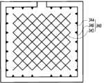
图4显示为本发明的一实施例的遮蔽电极层的上视示意图。请参照图4,遮蔽电极层340可以包括多条遮蔽电极条342、一遮蔽电极环344以及多个凸起346。遮蔽电极环344实质上环绕遮蔽电极条342所构成的网状图案,而各凸起346位于遮蔽电极环344上。各凸起346具有一尖端(未标示),尖端指向邻近的遮蔽电极条342的一端部。一但有静电荷累积的情形,遮蔽电极条342可以传输这些静电荷,并且利用尖端放电的形式将静电荷通过凸起346以及遮蔽电极环344传导出去。FIG. 4 is a schematic top view of a shielding electrode layer according to an embodiment of the present invention. Referring to FIG. 4 , the shielding electrode layer 340 may include a plurality of shielding
此外,图5及图6显示为本发明的另一实施例的遮蔽电极层的上视示意图。请参照图5,遮蔽电极层440在本实施例中包括多个遮蔽电极条442,且遮蔽电极条442连接成多个交叉遮蔽图案444。各交叉遮蔽图案444的一末端444T与另一交叉图案444的另一末端444T彼此相对。遮蔽电极层440应用于图2所显示的触控显示装置200时,各交叉遮蔽图案444正投影于显示面板210上的面积可选择性地不重叠于第一感测串列222A的第一连接线C1以及第二感测串列222B的第二连接线C2。当然,如图6所示,遮蔽电极层440也可以选择地进一步包括一遮蔽电极环446及多个凸起448。遮蔽电极环446实质上环绕交叉遮蔽图案444,而各凸起448位于遮蔽电极环446上。值得一提的是,各凸起448具有一尖端(未标示),其中尖端指向邻近的交叉遮蔽图案444的一末端。In addition, FIG. 5 and FIG. 6 are schematic top views showing a shielding electrode layer according to another embodiment of the present invention. Referring to FIG. 5 , the shielding
由以上所描述的实施方式可知,本发明并不特别地限定遮蔽电极层的图案设计。凡是遮蔽电极层的图案在显示面板上的正投影面积至少填满感测电极的间距就可以提供良好的光学补偿作用。此外,遮蔽电极层的图案在显示面板上的正投影面积略微地重迭感测电极在显示面板上的正投影面积更可以在斜向视角上提供光学补偿的作用。It can be seen from the above described embodiments that the present invention does not specifically limit the pattern design of the shielding electrode layer. As long as the orthographic projection area of the pattern of the shielding electrode layer on the display panel at least fills the distance between the sensing electrodes, a good optical compensation effect can be provided. In addition, the orthographic projection area of the pattern of the shielding electrode layer on the display panel slightly overlaps the orthographic projection area of the sensing electrode on the display panel, which can provide optical compensation for oblique viewing angles.
以下将以数个实施例说明图2的触控显示装置200中,触控面板与遮蔽电极层在剖面结构上的设计。当然,以下的实施例仅是举例说明之用,并非用来限定本发明。The design of the cross-sectional structure of the touch panel and the shielding electrode layer in the touch display device 200 of FIG. 2 will be described below with several embodiments. Certainly, the following examples are only used for illustration, and are not intended to limit the present invention.
图7显示为图2的触控显示装置中,触控面板与遮蔽电极层在剖面结构上的一第一种设计。请同时参照图2与图7,除了图2所显示的一基板224、第一感测串列222A与第二感测串列222B外,触控面板220实质上还包括一绝缘层226。第一感测串列222A的第一连接线C1位于基板224与绝缘层226之间,而绝缘层226位于基板224与第二感测串列222B之间。FIG. 7 shows a first design of the cross-sectional structure of the touch panel and the shielding electrode layer in the touch display device of FIG. 2 . Please refer to FIG. 2 and FIG. 7 at the same time. In addition to a
以本实施例而言,绝缘层226例如是由多个岛状绝缘图案所组成,而绝缘元件230例如是一绝缘层。遮蔽电极层240的配置位置则至少位于两个感测电极之间。此外,第一连接线C1以及第二连接线C2的材质可以是金属或透明导电材料。In this embodiment, the insulating
图8显示为图2的触控显示装置中,触控面板与遮蔽电极层在剖面结构上的一第二种设计。请参照图8,在本实施例中,触控面板与遮蔽电极层的设计与图7所述的实施例大致相似,其差异之处在于图8的绝缘层326除了覆盖第一连接线C1外,绝缘层326实质上还覆盖住第二感测电极E2。此外,绝缘层326具有开口326a以使第二连接线C2通过开口326a电性连接于第二感测电极E2。FIG. 8 shows a second design of the cross-sectional structure of the touch panel and the shielding electrode layer in the touch display device of FIG. 2 . Please refer to FIG. 8 , in this embodiment, the design of the touch panel and the shielding electrode layer is roughly similar to that of the embodiment described in FIG. 7 , the difference is that the insulating
图9显示为图2的触控显示装置中,触控面板与遮蔽电极层在剖面结构上的一第三种设计。请同时参照图2与图9,除了第一感测串列222A与第二感测串列222B外,触控面板220还包括有基板424以及绝缘层426,其中第一感测串列222A位于基板424与绝缘层426之间,而绝缘层426位于基板424与第二感测串列222B之间。此外,本实施例的绝缘元件230例如是一绝缘基板。所以,第二感测串列222B与遮蔽电极层240可以分别地制作于绝缘元件230的相对两侧。换言之,触控面板220例如是由基板424与绝缘元件230组立而成。在此,绝缘层426例如是由一光学胶或空气层等透光的绝缘材料所组成。FIG. 9 shows a third design of the cross-sectional structure of the touch panel and the shielding electrode layer in the touch display device of FIG. 2 . Please refer to FIG. 2 and FIG. 9 at the same time. In addition to the
图10显示为图2的触控显示装置中,触控面板与遮蔽电极层在剖面结构上的一第四种设计。请同时参照图2与图10,本实施例中,绝缘元件230例如是一绝缘层,其配置于触控面板220与遮蔽电极层240之间。另外,除了第一感测串列222A与第二感测串列222B外,触控面板220还包括基板524、基板526以及一绝缘层528。第一感测串列222A系制作于基板524上,而第二感测串列222B系制作于基板526上。绝缘层528配置于第一感测串列222A与基板526之间并且绝缘层528与第二感测串列222B分别配置于基板526的相对两侧。在此,绝缘层528例如是一光学胶或一空气层等透明绝缘层。FIG. 10 shows a fourth design of the cross-sectional structure of the touch panel and the shielding electrode layer in the touch display device of FIG. 2 . Please refer to FIG. 2 and FIG. 10 at the same time. In this embodiment, the insulating
图11显示为图2的触控显示装置中,触控面板与遮蔽电极层在剖面结构上的一第五种设计。请同时参照图2与图11,触控面板220包括多个第一感测串列222A、多个第二感测串列222B以及一基板624,其中第一感测串列222A与第二感测串列222B分别地配置于基板624的相对两侧。在本实施例中,绝缘元件230例如是一绝缘层,而配置于遮蔽电极层240与第二感测串列222B之间。另外,为了保护第一感测串列222A,可将保护层600配置于第一感测串列222A上。FIG. 11 shows a fifth design of the cross-sectional structure of the touch panel and the shielding electrode layer in the touch display device of FIG. 2 . Please refer to FIG. 2 and FIG. 11 at the same time, the touch panel 220 includes a plurality of
综上所述,本发明将图案化的遮蔽电极层配置于显示面板与触控面板之间。图案化的遮蔽电极层除了可具有信号屏蔽的作用以及防止静电放电的作用外,遮蔽电极层的图案设计还有助于改善触控显示装置的显示不均匀的现象。具体来说,遮蔽电极层与触控面板的感测电极具有相同材质。所以,本发明将遮蔽电极层的图案设置于感测电极的间距中以使显示面板的显示光线在不同位置上都会经过一层透明导电层。如此一来,触控显示装置将具有更为均匀的显示效果。To sum up, the present invention disposes the patterned shielding electrode layer between the display panel and the touch panel. In addition to the function of signal shielding and electrostatic discharge prevention, the patterned shielding electrode layer also helps to improve the display unevenness of the touch display device. Specifically, the shielding electrode layer has the same material as the sensing electrodes of the touch panel. Therefore, in the present invention, the pattern of the shielding electrode layer is arranged in the distance between the sensing electrodes so that the display light of the display panel will pass through a transparent conductive layer at different positions. In this way, the touch display device will have a more uniform display effect.
虽然本发明已以实施例揭示如上,然其并非用以限定本发明,任何所属技术领域的普通技术人员,当可作些许的更动与润饰,而不脱离本发明的精神和范围内。Although the present invention has been disclosed above with the embodiments, it is not intended to limit the present invention. Any person skilled in the art may make some changes and modifications without departing from the spirit and scope of the present invention.
Claims (10)
Priority Applications (1)
| Application Number | Priority Date | Filing Date | Title |
|---|---|---|---|
| CN2010106241291ACN102541339A (en) | 2010-12-29 | 2010-12-29 | touch display device |
Applications Claiming Priority (1)
| Application Number | Priority Date | Filing Date | Title |
|---|---|---|---|
| CN2010106241291ACN102541339A (en) | 2010-12-29 | 2010-12-29 | touch display device |
Publications (1)
| Publication Number | Publication Date |
|---|---|
| CN102541339Atrue CN102541339A (en) | 2012-07-04 |
Family
ID=46348372
Family Applications (1)
| Application Number | Title | Priority Date | Filing Date |
|---|---|---|---|
| CN2010106241291APendingCN102541339A (en) | 2010-12-29 | 2010-12-29 | touch display device |
Country Status (1)
| Country | Link |
|---|---|
| CN (1) | CN102541339A (en) |
Cited By (9)
| Publication number | Priority date | Publication date | Assignee | Title |
|---|---|---|---|---|
| CN103440065A (en)* | 2013-07-31 | 2013-12-11 | 南昌欧菲光科技有限公司 | Touch control element |
| CN104156129A (en)* | 2014-07-11 | 2014-11-19 | 京东方科技集团股份有限公司 | Touch substrate and display device |
| JP2017513170A (en)* | 2015-03-23 | 2017-05-25 | 小米科技有限責任公司Xiaomi Inc. | Touch circuit and touch panel having electrostatic protection structure |
| TWI630519B (en)* | 2014-02-21 | 2018-07-21 | 韓商海帝士科技公司 | Touch panel having overcoating layer for reducing moire pattern, liquid crystal display device including touch panel and method of forming touch panel |
| CN110502150A (en)* | 2019-01-30 | 2019-11-26 | 友达光电股份有限公司 | touch device |
| CN110658943A (en)* | 2018-06-29 | 2020-01-07 | 乐金显示有限公司 | Touch display panel and touch display device |
| CN112860097A (en)* | 2019-11-26 | 2021-05-28 | 三星显示有限公司 | Electronic device |
| CN112905067A (en)* | 2021-04-12 | 2021-06-04 | 厦门天马微电子有限公司 | Touch panel and touch display device |
| CN114185461A (en)* | 2021-12-13 | 2022-03-15 | 昆山国显光电有限公司 | Touch panel, display panel and touch panel manufacturing method |
Citations (5)
| Publication number | Priority date | Publication date | Assignee | Title |
|---|---|---|---|---|
| CN101694605A (en)* | 2009-10-27 | 2010-04-14 | 友达光电股份有限公司 | Touch panel |
| CN101702108A (en)* | 2009-11-13 | 2010-05-05 | 友达光电股份有限公司 | Touch substrate |
| CN101719038A (en)* | 2009-12-30 | 2010-06-02 | 友达光电股份有限公司 | Touch display panel and touch substrate |
| CN101763202A (en)* | 2010-01-12 | 2010-06-30 | 友达光电股份有限公司 | Capacitive touch display panel and capacitive touch display substrate |
| CN101882040A (en)* | 2010-03-12 | 2010-11-10 | 敦泰科技有限公司 | Mutual capacitive touch screen with electrodes arranged on a double-layer conductive material film |
- 2010
- 2010-12-29CNCN2010106241291Apatent/CN102541339A/enactivePending
Patent Citations (5)
| Publication number | Priority date | Publication date | Assignee | Title |
|---|---|---|---|---|
| CN101694605A (en)* | 2009-10-27 | 2010-04-14 | 友达光电股份有限公司 | Touch panel |
| CN101702108A (en)* | 2009-11-13 | 2010-05-05 | 友达光电股份有限公司 | Touch substrate |
| CN101719038A (en)* | 2009-12-30 | 2010-06-02 | 友达光电股份有限公司 | Touch display panel and touch substrate |
| CN101763202A (en)* | 2010-01-12 | 2010-06-30 | 友达光电股份有限公司 | Capacitive touch display panel and capacitive touch display substrate |
| CN101882040A (en)* | 2010-03-12 | 2010-11-10 | 敦泰科技有限公司 | Mutual capacitive touch screen with electrodes arranged on a double-layer conductive material film |
Cited By (14)
| Publication number | Priority date | Publication date | Assignee | Title |
|---|---|---|---|---|
| CN103440065B (en)* | 2013-07-31 | 2016-07-06 | 南昌欧菲光科技有限公司 | Touch control component |
| CN103440065A (en)* | 2013-07-31 | 2013-12-11 | 南昌欧菲光科技有限公司 | Touch control element |
| TWI630519B (en)* | 2014-02-21 | 2018-07-21 | 韓商海帝士科技公司 | Touch panel having overcoating layer for reducing moire pattern, liquid crystal display device including touch panel and method of forming touch panel |
| CN104156129A (en)* | 2014-07-11 | 2014-11-19 | 京东方科技集团股份有限公司 | Touch substrate and display device |
| JP2017513170A (en)* | 2015-03-23 | 2017-05-25 | 小米科技有限責任公司Xiaomi Inc. | Touch circuit and touch panel having electrostatic protection structure |
| US10152165B2 (en) | 2015-03-23 | 2018-12-11 | Xiaomi Inc. | Touch panel circuit with electrostatic discharge protection structure and touch panel including same |
| CN110658943B (en)* | 2018-06-29 | 2023-05-12 | 乐金显示有限公司 | Touch display panel and touch display device |
| CN110658943A (en)* | 2018-06-29 | 2020-01-07 | 乐金显示有限公司 | Touch display panel and touch display device |
| CN110502150A (en)* | 2019-01-30 | 2019-11-26 | 友达光电股份有限公司 | touch device |
| CN110502150B (en)* | 2019-01-30 | 2023-03-31 | 友达光电股份有限公司 | Touch control device |
| CN112860097A (en)* | 2019-11-26 | 2021-05-28 | 三星显示有限公司 | Electronic device |
| CN112905067A (en)* | 2021-04-12 | 2021-06-04 | 厦门天马微电子有限公司 | Touch panel and touch display device |
| CN114185461A (en)* | 2021-12-13 | 2022-03-15 | 昆山国显光电有限公司 | Touch panel, display panel and touch panel manufacturing method |
| CN114185461B (en)* | 2021-12-13 | 2023-09-22 | 昆山国显光电有限公司 | Touch panel, display panel and touch panel manufacturing method |
Similar Documents
| Publication | Publication Date | Title |
|---|---|---|
| TWI403795B (en) | Touch display apparatus | |
| CN102541339A (en) | touch display device | |
| CN102467309B (en) | Capacitive touch panel and manufacturing method thereof | |
| CN101639580B (en) | Display device | |
| US20150085205A1 (en) | Touch panel | |
| US9097928B2 (en) | Capacitive touch panel and display device | |
| US20130194213A1 (en) | Touch-sensing panel and touch-sensing display apparatus | |
| US20120113021A1 (en) | Touch panel device | |
| KR20150069950A (en) | Touch panel | |
| KR102195392B1 (en) | Touch panel | |
| TW201715365A (en) | Touch display device and driving method thereof | |
| CN102043548A (en) | capacitive touch panel | |
| TWI546723B (en) | Transparent electrode layer, touch panel and electronic device | |
| TWI470495B (en) | Touch-sensing subsrate, display panel, and patterned light-shielding layer | |
| CN106155411A (en) | Touch screen, touch panel, display device and electronic equipment | |
| KR20150072838A (en) | Touch panel | |
| KR101241469B1 (en) | Touch panel | |
| TWI398809B (en) | Capacitive touch panel | |
| TWI597633B (en) | Touch panel capable of reducing exposure of etching wires | |
| KR102254179B1 (en) | Touch display apparatus | |
| CN106406644A (en) | Touchscreen panel | |
| US20160349873A1 (en) | Touch panel and display device | |
| KR102281616B1 (en) | Touch screen panel and method of manufacturing the same | |
| US10705661B2 (en) | Touch device | |
| JP2012123850A (en) | Electrostatic capacitance coupling-type touch panel |
Legal Events
| Date | Code | Title | Description |
|---|---|---|---|
| C06 | Publication | ||
| PB01 | Publication | ||
| C10 | Entry into substantive examination | ||
| SE01 | Entry into force of request for substantive examination | ||
| C02 | Deemed withdrawal of patent application after publication (patent law 2001) | ||
| WD01 | Invention patent application deemed withdrawn after publication | Application publication date:20120704 |