CN102530854A - Method for preparing semiconductor single-walled carbon nanotube by adopting a room-temperature plasma etching method - Google Patents
Method for preparing semiconductor single-walled carbon nanotube by adopting a room-temperature plasma etching methodDownload PDFInfo
- Publication number
- CN102530854A CN102530854ACN2012100143576ACN201210014357ACN102530854ACN 102530854 ACN102530854 ACN 102530854ACN 2012100143576 ACN2012100143576 ACN 2012100143576ACN 201210014357 ACN201210014357 ACN 201210014357ACN 102530854 ACN102530854 ACN 102530854A
- Authority
- CN
- China
- Prior art keywords
- carbon nanotubes
- walled carbon
- plasma etching
- room temperature
- semiconducting single
- Prior art date
- Legal status (The legal status is an assumption and is not a legal conclusion. Google has not performed a legal analysis and makes no representation as to the accuracy of the status listed.)
- Pending
Links
Images


Landscapes
- Carbon And Carbon Compounds (AREA)
Abstract
Translated fromChinese
Description
Translated fromChinese技术领域technical field
本发明属于纳米材料制备技术领域,尤其是涉及一种室温等离子体刻蚀制备半导体性单壁碳纳米管的方法。The invention belongs to the technical field of nanomaterial preparation, and in particular relates to a method for preparing semiconductor single-wall carbon nanotubes by plasma etching at room temperature.
背景技术Background technique
单壁碳纳米管(Single-walled Carbon nanotubes;SWNT)根据手性与直径的不同可分为金属性和半导体性单壁碳纳米管两种。众所周知,SWNT因具有卓越的机械性能、独特的电学、光学性能而被广泛应用在场效应晶体管、太阳能电池、气体传感器、储氢等诸多领域。尤其是半导体性SWNT被认为是一种准一维的纳米材料,其具有高载流子迁移率等优点而有望取代硅材料而成为下一代微电子器件的关键材料。但是在目前得到的SWNT产物中往往是金属性和半导体性SWNT混合在一起,因此无法直接用于制作纳电子器件,已经成为当前SWNT应用于高性能纳电子器件过程中所面临的一个重要的难题。Single-walled carbon nanotubes (Single-walled Carbon nanotubes; SWNT) can be divided into metallic and semiconducting single-walled carbon nanotubes according to their chirality and diameter. As we all know, SWNTs are widely used in field effect transistors, solar cells, gas sensors, hydrogen storage and many other fields due to their excellent mechanical properties, unique electrical and optical properties. In particular, semiconducting SWNT is considered as a quasi-one-dimensional nanomaterial, which has the advantages of high carrier mobility and is expected to replace silicon and become the key material for the next generation of microelectronic devices. However, the currently obtained SWNT products are often mixed with metallic and semiconducting SWNTs, so they cannot be directly used to make nanoelectronic devices, which has become an important problem in the process of applying SWNTs to high-performance nanoelectronic devices. .
全世界范围的科学家尝试了各种方式试图得到单一导电属性的单壁碳纳米管,归纳起来可分为择优制备、金属/半导体分离和选择性刻蚀三种途径。相比困难的择优制备,后两种途径更容易得到半导体性SWNT。Dai HJ等人2006年在Science上发表题为“Selective etching of metallic carbon nanotubes by gas-phase reaction”的论文,验证了等离子体选择性金属性SWNT从而得到半导体性SWNT这一结论。但该等离子体刻蚀过程中在一定的温度下才能进行,而且需要选择特定的气体才有较好的选择性刻蚀效果。Scientists around the world have tried various methods to obtain single-walled carbon nanotubes with a single conductive property, which can be summarized into three ways: preferential preparation, metal/semiconductor separation and selective etching. Compared with the difficult preferential preparation, the latter two approaches are easier to obtain semiconducting SWNTs. Dai HJ et al. published a paper entitled "Selective etching of metallic carbon nanotubes by gas-phase reaction" in Science in 2006, which verified the conclusion that plasma selective metallic SWNTs were obtained to obtain semiconducting SWNTs. However, the plasma etching process can only be carried out at a certain temperature, and a specific gas needs to be selected to have a better selective etching effect.
发明内容Contents of the invention
本发明的目的就是为了克服上述现有技术存在的缺陷而提供一种室温下等离子体刻蚀法制备半导体性单壁碳纳米管的方法,本发明采用对单壁碳纳米管进行等离子体刻蚀以便去除金属性单壁碳纳米管,从而得到半导体性单壁碳纳米管。The purpose of the present invention is to provide a method for preparing semiconducting single-walled carbon nanotubes by plasma etching at room temperature in order to overcome the defects in the above-mentioned prior art. The present invention uses plasma etching of single-walled carbon nanotubes In order to remove metallic single-walled carbon nanotubes, thereby obtaining semiconducting single-walled carbon nanotubes.
本发明的目的可以通过以下技术方案来实现:The purpose of the present invention can be achieved through the following technical solutions:
室温等离子体刻蚀制备半导体性单壁碳纳米管的方法,包括以下步骤:A method for preparing semiconducting single-walled carbon nanotubes by plasma etching at room temperature, comprising the following steps:
(1)将均匀分散在有机溶剂中的碳纳米管滴在载玻片上并烘干;(1) drop carbon nanotubes uniformly dispersed in an organic solvent on a glass slide and dry;
(2)将烘干后载玻片放入等离子处理设备中并抽真空至10-2Pa;(2) Put the dried glass slide into the plasma processing equipment and vacuumize to 10-2 Pa;
(3)调节等离子体处理腔内低压气体的压力、等离子体功率、刻蚀时间实现对金属性单壁碳纳米管的刻蚀,留下半导体性单壁碳纳米管,即为产品。(3) Adjust the pressure of the low-pressure gas in the plasma processing chamber, the plasma power, and the etching time to etch the metallic single-walled carbon nanotubes, and leave the semiconducting single-walled carbon nanotubes as the product.
所述的有机溶剂为N、N-二甲基甲酰胺、异丙醇或乙醇。The organic solvent is N,N-dimethylformamide, isopropanol or ethanol.
所述的碳纳米管在有机溶剂中的固含量为5~20mg/100ml。The solid content of the carbon nanotubes in the organic solvent is 5-20mg/100ml.
所述的低压气体为单质气体,包括氩气、氦气、氮气、氢气或氧气。The low-pressure gas is elemental gas, including argon, helium, nitrogen, hydrogen or oxygen.
所述的低压气体为化合物气体,包括一氧化碳、二氧化碳或甲烷。The low-pressure gas is a compound gas, including carbon monoxide, carbon dioxide or methane.
所述的低压气体的压力为1~100Pa。The pressure of the low-pressure gas is 1-100Pa.
所述的等离子体功率为10~100W。The plasma power is 10-100W.
所述的刻蚀时间为0.1~60min。The etching time is 0.1-60 min.
与现有技术相比,本发明采用室温等离子体选择性刻蚀制备半导体性单壁碳纳米管,工艺简单、便于大面积制备半导体单壁碳纳米管。Compared with the prior art, the invention adopts room-temperature plasma selective etching to prepare semiconductive single-wall carbon nanotubes, has simple process and is convenient for large-scale preparation of semiconductive single-wall carbon nanotubes.
附图说明Description of drawings
图1为实施例1中经等离子体刻蚀后单壁碳纳米管的扫描电镜(SEM)照片;Fig. 1 is the scanning electron microscope (SEM) photo of single-walled carbon nanotubes after plasma etching in embodiment 1;
图2为实施例1中等离子体刻蚀前后单壁碳纳米管的紫外-可见-近红外吸收谱变化;Fig. 2 is the ultraviolet-visible-near-infrared absorption spectrum change of single-walled carbon nanotubes before and after plasma etching in embodiment 1;
图3为实施例2中经等离子体刻蚀后单壁碳纳米管的紫外-可见-近红外吸收谱。FIG. 3 is the ultraviolet-visible-near-infrared absorption spectrum of single-walled carbon nanotubes after plasma etching in Example 2. FIG.
具体实施方式Detailed ways
下面结合附图和具体实施例对本发明进行详细说明。The present invention will be described in detail below in conjunction with the accompanying drawings and specific embodiments.
实施例1Example 1
步骤一:称量10mg纯单壁碳纳米管与100ml N、N-二甲基甲酰胺混合并超声分散均匀,然后将分散的SWNT溶液滴在洁净的载玻片上并烘干以便形成一层具有一定厚度的SWNT薄膜。Step 1: Weigh 10 mg of pure single-walled carbon nanotubes and mix them with 100 ml of N, N-dimethylformamide and disperse evenly by ultrasonic, then drop the dispersed SWNT solution on a clean glass slide and dry to form a layer with A certain thickness of SWNT film.
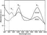
步骤二:将干燥后的SWNT薄膜放入等离子体刻蚀腔体中抽真空至10-2Pa,然后通入高纯氩气,通过调节流量使得腔体内压力保持在6Pa,打开射频电源使等离子体功率20w连续刻蚀15min。刻蚀结束后关闭射频电源、氩气并缓慢放气、取出样品。处理后的单壁碳纳米管即为半导体性单壁碳纳米管。图1为刻蚀后的扫描电镜(SEM)图片,从图可知单壁碳纳米管被刻蚀形成碳杂质。而从样品的紫外-可见-近红外吸收光谱(图2)中可以看出600~850nm范围内金属性SWNT的吸收强度大大降低,说明金属性SWNT已经被刻蚀掉。Step 2: Put the dried SWNT film into the plasma etching chamber to evacuate to 10-2 Pa, then introduce high-purity argon gas, keep the pressure in the chamber at 6 Pa by adjusting the flow rate, and turn on the radio frequency power to make the plasma The volume power is 20w and it is etched continuously for 15min. After the etching is finished, turn off the RF power supply, argon gas and slowly release the gas, and take out the sample. The treated single-wall carbon nanotubes are semiconducting single-wall carbon nanotubes. FIG. 1 is a scanning electron microscope (SEM) picture after etching. It can be seen from the figure that the single-walled carbon nanotubes are etched to form carbon impurities. From the ultraviolet-visible-near-infrared absorption spectrum of the sample (Figure 2), it can be seen that the absorption intensity of the metallic SWNT in the range of 600-850 nm is greatly reduced, indicating that the metallic SWNT has been etched away.
实施例2Example 2
步骤一:称量15mg纯单壁碳纳米管与150ml N、N-二甲基甲酰胺混合并超声分散均匀,然后将分散的SWNT溶液滴在洁净的载玻片上并烘干以便形成一层具有一定厚度的SWNT薄膜。Step 1: Weigh 15 mg of pure single-walled carbon nanotubes and mix them with 150 ml of N, N-dimethylformamide and disperse evenly by ultrasonic, then drop the dispersed SWNT solution on a clean glass slide and dry it to form a layer with A certain thickness of SWNT film.
步骤二:将干燥后的SWNT薄膜放入等离子体刻蚀腔体中抽真空至10-2Pa,然后通入高纯氦气,通过调节流量使得腔体内压力保持在3Pa,打开射频电源使等离子体功率10w连续刻蚀60min。刻蚀结束后关闭射频电源、氦气并缓慢放气、取出样品。处理后的单壁碳纳米管即为半导体性单壁碳纳米管。图3为等离子体刻蚀后的的紫外-可见-近红外吸收光谱,从图可以看出600~850nm范围内金属性SWNT的吸收强度大大降低,说明金属性SWNT已经被刻蚀掉。Step 2: Put the dried SWNT film into the plasma etching chamber to evacuate to 10-2 Pa, then introduce high-purity helium, adjust the flow rate to keep the pressure in the chamber at 3 Pa, turn on the radio frequency power to make the plasma Volume power 10w continuous etching for 60min. After the etching is finished, turn off the RF power supply, helium gas and slowly release the gas, and take out the sample. The treated single-wall carbon nanotubes are semiconducting single-wall carbon nanotubes. Figure 3 is the ultraviolet-visible-near-infrared absorption spectrum after plasma etching. It can be seen from the figure that the absorption intensity of the metallic SWNT in the range of 600-850nm is greatly reduced, indicating that the metallic SWNT has been etched away.
实施例3Example 3
步骤一:称量20mg纯单壁碳纳米管与200ml异丙醇混合并超声分散均匀,然后将分散的SWNT溶液滴在洁净的载玻片上并烘干以便形成一层具有一定厚度的SWNT薄膜。Step 1: Weigh 20 mg of pure single-walled carbon nanotubes and mix them with 200 ml of isopropanol and disperse evenly by ultrasonic, then drop the dispersed SWNT solution on a clean glass slide and dry to form a layer of SWNT film with a certain thickness.
步骤二:将干燥后的SWNT薄膜放入等离子体刻蚀腔体中抽真空至10-2Pa,然后通入高纯氢气,通过调节流量使得腔体内压力保持在1Pa,打开射频电源使等离子体功率100w连续刻蚀0.1min。刻蚀结束后关闭射频电源、氢气并缓慢放气、取出样品。处理后的单壁碳纳米管即为半导体性单壁碳纳米管。Step 2: Put the dried SWNT film into the plasma etching chamber to evacuate to 10-2 Pa, then introduce high-purity hydrogen, adjust the flow rate to keep the pressure in the chamber at 1Pa, turn on the radio frequency power to make the plasma Power 100w continuous etching 0.1min. After the etching is finished, turn off the RF power supply, hydrogen gas and slowly release the gas, and take out the sample. The treated single-wall carbon nanotubes are semiconducting single-wall carbon nanotubes.
实施例4Example 4
步骤一:称量5mg纯单壁碳纳米管与100ml N、N-二甲基甲酰胺混合并超声分散均匀,然后将分散的SWNT溶液滴在洁净的载玻片上并烘干以便形成一层具有一定厚度的SWNT薄膜。Step 1: Weigh 5 mg of pure single-walled carbon nanotubes and mix them with 100 ml of N, N-dimethylformamide and disperse evenly by ultrasonic, then drop the dispersed SWNT solution on a clean glass slide and dry it to form a layer with A certain thickness of SWNT film.
步骤二:将干燥后的SWNT薄膜放入等离子体刻蚀腔体中抽真空至10-2Pa,然后通入高纯氮气,通过调节流量使得腔体内压力保持在100Pa,打开射频电源使等离子体功率50w连续刻蚀25min。刻蚀结束后关闭射频电源、氮气并缓慢放气、取出样品。处理后的单壁碳纳米管即为半导体性单壁碳纳米管。Step 2: Put the dried SWNT film into the plasma etching chamber to evacuate to 10-2 Pa, then introduce high-purity nitrogen gas, adjust the flow rate to keep the pressure in the chamber at 100 Pa, and turn on the radio frequency power to make the plasma Power 50w continuous etching for 25min. After the etching, turn off the RF power supply, nitrogen gas and slowly release the gas, and take out the sample. The treated single-wall carbon nanotubes are semiconducting single-wall carbon nanotubes.
实施例5Example 5
步骤一:称量10mg纯单壁碳纳米管与150ml乙醇混合并超声分散均匀,然后将分散的SWNT溶液滴在洁净的载玻片上并烘干以便形成一层具有一定厚度的SWNT薄膜。Step 1: Weigh 10 mg of pure single-walled carbon nanotubes and mix them with 150 ml of ethanol and disperse them uniformly by ultrasonic, then drop the dispersed SWNT solution on a clean glass slide and dry it to form a layer of SWNT film with a certain thickness.
步骤二:将干燥后的SWNT薄膜放入等离子体刻蚀腔体中抽真空至10-2Pa,然后通入高纯甲烷气,通过调节流量使得腔体内压力保持在10Pa,打开射频电源使等离子体功率50w连续刻蚀35min。刻蚀结束后关闭射频电源、甲烷气并缓慢放气、取出样品。处理后的单壁碳纳米管即为半导体性单壁碳纳米管。Step 2: Put the dried SWNT film into the plasma etching chamber to evacuate to 10-2 Pa, then introduce high-purity methane gas, adjust the flow rate to keep the pressure in the chamber at 10 Pa, and turn on the radio frequency power to make the plasma Volume power 50w continuous etching for 35min. After etching, turn off the RF power supply, methane gas and slowly deflate, and take out the sample. The treated single-wall carbon nanotubes are semiconducting single-wall carbon nanotubes.
实施例6Example 6
步骤一:称量20mg纯单壁碳纳米管与100ml N、N-二甲基甲酰胺混合并超声分散均匀,然后将分散的SWNT溶液滴在洁净的载玻片上并烘干以便形成一层具有一定厚度的SWNT薄膜。Step 1: Weigh 20 mg of pure single-walled carbon nanotubes and mix them with 100 ml of N, N-dimethylformamide and disperse evenly by ultrasonic, then drop the dispersed SWNT solution on a clean glass slide and dry it to form a layer with A certain thickness of SWNT film.
步骤二:将干燥后的SWNT薄膜放入等离子体刻蚀腔体中抽真空至10-2Pa,然后通入高纯一氧化碳气体,通过调节流量使得腔体内压力保持在6Pa,打开射频电源使等离子体功率20w连续刻蚀20min。刻蚀结束后关闭射频电源、一氧化碳气体并缓慢放气、取出样品。处理后的单壁碳纳米管即为半导体性单壁碳纳米管。Step 2: Put the dried SWNT film into the plasma etching chamber to evacuate to 10-2 Pa, then introduce high-purity carbon monoxide gas, adjust the flow rate to keep the pressure in the chamber at 6 Pa, turn on the radio frequency power to make the plasma Volume power 20w continuous etching for 20min. After the etching is finished, turn off the RF power supply, carbon monoxide gas and slowly deflate, and take out the sample. The treated single-wall carbon nanotubes are semiconducting single-wall carbon nanotubes.
上述所有实施例都是在以本发明技术方案为前提下进行实施,给出了详细实施方式和具体的操作过程,但本发明的保护范围不限于下述的实施例。All the above-mentioned embodiments are implemented on the premise of the technical solution of the present invention, and detailed implementation methods and specific operation processes are provided, but the protection scope of the present invention is not limited to the following embodiments.
Claims (8)
Translated fromChinesePriority Applications (1)
| Application Number | Priority Date | Filing Date | Title |
|---|---|---|---|
| CN2012100143576ACN102530854A (en) | 2012-01-17 | 2012-01-17 | Method for preparing semiconductor single-walled carbon nanotube by adopting a room-temperature plasma etching method |
Applications Claiming Priority (1)
| Application Number | Priority Date | Filing Date | Title |
|---|---|---|---|
| CN2012100143576ACN102530854A (en) | 2012-01-17 | 2012-01-17 | Method for preparing semiconductor single-walled carbon nanotube by adopting a room-temperature plasma etching method |
Publications (1)
| Publication Number | Publication Date |
|---|---|
| CN102530854Atrue CN102530854A (en) | 2012-07-04 |
Family
ID=46339085
Family Applications (1)
| Application Number | Title | Priority Date | Filing Date |
|---|---|---|---|
| CN2012100143576APendingCN102530854A (en) | 2012-01-17 | 2012-01-17 | Method for preparing semiconductor single-walled carbon nanotube by adopting a room-temperature plasma etching method |
Country Status (1)
| Country | Link |
|---|---|
| CN (1) | CN102530854A (en) |
Cited By (5)
| Publication number | Priority date | Publication date | Assignee | Title |
|---|---|---|---|---|
| CN103883872A (en)* | 2014-03-14 | 2014-06-25 | 北京大学 | Porous nanotube storage medium and method for gas storage |
| CN109256467A (en)* | 2018-09-07 | 2019-01-22 | 苏州欣替纳米科技有限公司 | High-performance single wall carbon nano-tube film transistor and preparation method thereof |
| CN109406586A (en)* | 2017-08-18 | 2019-03-01 | 蓝思科技(长沙)有限公司 | Production method of carbon nano tube sensor and application thereof |
| CN114348992A (en)* | 2021-12-15 | 2022-04-15 | 中国科学院金属研究所 | An efficient and controllable method for gas-phase chopped carbon nanotubes |
| CN116102003A (en)* | 2022-12-13 | 2023-05-12 | 中国科学院金属研究所 | Dry method preparation method of narrow band gap distribution high-purity semiconductor single-walled carbon nanotube from top to bottom |
Citations (4)
| Publication number | Priority date | Publication date | Assignee | Title |
|---|---|---|---|---|
| US20050184294A1 (en)* | 2004-01-21 | 2005-08-25 | Yuegang Zhang | End functionalization of carbon nanotubes |
| CN1794086A (en)* | 2006-01-12 | 2006-06-28 | 上海交通大学 | Method of covering and patterning nanometer structure on sensitive material surface |
| CN101540285A (en)* | 2009-04-16 | 2009-09-23 | 上海交通大学 | Method for preparing carbon nano tube thin-film field-effect transistor |
| KR20100130695A (en)* | 2009-06-04 | 2010-12-14 | 한양대학교 산학협력단 | Carbon pattern formation method using oxygen plasma |
- 2012
- 2012-01-17CNCN2012100143576Apatent/CN102530854A/enactivePending
Patent Citations (4)
| Publication number | Priority date | Publication date | Assignee | Title |
|---|---|---|---|---|
| US20050184294A1 (en)* | 2004-01-21 | 2005-08-25 | Yuegang Zhang | End functionalization of carbon nanotubes |
| CN1794086A (en)* | 2006-01-12 | 2006-06-28 | 上海交通大学 | Method of covering and patterning nanometer structure on sensitive material surface |
| CN101540285A (en)* | 2009-04-16 | 2009-09-23 | 上海交通大学 | Method for preparing carbon nano tube thin-film field-effect transistor |
| KR20100130695A (en)* | 2009-06-04 | 2010-12-14 | 한양대학교 산학협력단 | Carbon pattern formation method using oxygen plasma |
Non-Patent Citations (2)
| Title |
|---|
| A HASSANIEN等: "Selective etching of metallic single-wall carbon nanotubes with hydrogen plasma", 《NANOTECHNOLOGY》, vol. 16, no. 2, 14 January 2005 (2005-01-14), pages 278 - 281* |
| GUANGYU ZHANG等: "Selective etching of metallic carbon nanotubes by gas-phase reaction", 《SCIENCE》, vol. 314, 10 November 2006 (2006-11-10), pages 974 - 976* |
Cited By (8)
| Publication number | Priority date | Publication date | Assignee | Title |
|---|---|---|---|---|
| CN103883872A (en)* | 2014-03-14 | 2014-06-25 | 北京大学 | Porous nanotube storage medium and method for gas storage |
| CN103883872B (en)* | 2014-03-14 | 2016-02-10 | 北京大学 | For porous nanotube storage medium and the method for atmosphere storage |
| CN109406586A (en)* | 2017-08-18 | 2019-03-01 | 蓝思科技(长沙)有限公司 | Production method of carbon nano tube sensor and application thereof |
| CN109256467A (en)* | 2018-09-07 | 2019-01-22 | 苏州欣替纳米科技有限公司 | High-performance single wall carbon nano-tube film transistor and preparation method thereof |
| CN114348992A (en)* | 2021-12-15 | 2022-04-15 | 中国科学院金属研究所 | An efficient and controllable method for gas-phase chopped carbon nanotubes |
| CN114348992B (en)* | 2021-12-15 | 2024-01-19 | 中国科学院金属研究所 | Method for efficiently and controllably chopping carbon nano tube in gas phase |
| CN116102003A (en)* | 2022-12-13 | 2023-05-12 | 中国科学院金属研究所 | Dry method preparation method of narrow band gap distribution high-purity semiconductor single-walled carbon nanotube from top to bottom |
| CN116102003B (en)* | 2022-12-13 | 2024-09-20 | 中国科学院金属研究所 | Dry method preparation method of narrow band gap distribution high-purity semiconductor single-walled carbon nanotube from top to bottom |
Similar Documents
| Publication | Publication Date | Title |
|---|---|---|
| Acik et al. | A review on thermal exfoliation of graphene oxide | |
| Li et al. | Controllable synthesis of graphene by plasma‐enhanced chemical vapor deposition and its related applications | |
| Zhu et al. | Healing of reduced graphene oxide with methane+ hydrogen plasma | |
| CN101195482B (en) | A method of growing semiconducting single-walled carbon nanotubes | |
| CN103265018B (en) | A kind of dielectric base is directly prepared the method for Graphene | |
| CN101717083A (en) | Graphene and preparation method thereof | |
| Zhang et al. | Combustion synthesis of N-doped three-dimensional graphene networks using graphene oxide–nitrocellulose composites | |
| CN102530854A (en) | Method for preparing semiconductor single-walled carbon nanotube by adopting a room-temperature plasma etching method | |
| CN102161482A (en) | Method for preparing graphene | |
| CN103145117B (en) | Method for preparing graphene | |
| CN106892426A (en) | The preparation method of Graphene and black phosphorus quantum dot composite material | |
| CN107026259A (en) | A kind of graphene combination electrode material and preparation method and application | |
| CN108821331B (en) | A kind of preparation method and product of gallium oxide nanorod | |
| CN103011130B (en) | The method of hydrogen in-situ weak etching growing high-quality semi-conductive single-walled carbon nanotubes | |
| CN101386408A (en) | A kind of semiconducting single-walled carbon nanotube and its preparation method | |
| Wang et al. | Conversion of pristine and p-doped sulfuric-acid-treated single-walled carbon nanotubes to n-type materials by a facile hydrazine vapor exposure process | |
| CN101671001B (en) | Preparation method for semiconductor single wall carbon nano tube | |
| CN102206867B (en) | Preparation method of graphene single crystal plate | |
| CN104418387B (en) | A kind of molybdenum disulfide nano thin slice and preparation method thereof | |
| CN103407988A (en) | Method for preparing graphene film at low temperature | |
| Bo et al. | Instantaneous reduction of graphene oxide paper for supercapacitor electrodes with unimpeded liquid permeation | |
| CN104118870A (en) | Preparation method of nitrogen-doped graphene and nitrogen-doped graphene | |
| CN104291339B (en) | A kind of preparation method of ultra-thin carbofrax material | |
| Dong et al. | Unzipping Carbon Nanotubes to Sub‐5‐nm Graphene Nanoribbons on Cu (111) by Surface Catalysis | |
| CN105129786A (en) | Preparing method for massive single-layer graphene |
Legal Events
| Date | Code | Title | Description |
|---|---|---|---|
| C06 | Publication | ||
| PB01 | Publication | ||
| C10 | Entry into substantive examination | ||
| SE01 | Entry into force of request for substantive examination | ||
| C12 | Rejection of a patent application after its publication | ||
| RJ01 | Rejection of invention patent application after publication | Application publication date:20120704 |