CN102522425B - Structure of ultrahigh pressure germanium-silicon heterojunction bipolar transistor (HBT) device and preparation method - Google Patents
Structure of ultrahigh pressure germanium-silicon heterojunction bipolar transistor (HBT) device and preparation methodDownload PDFInfo
- Publication number
- CN102522425B CN102522425BCN201110440342.1ACN201110440342ACN102522425BCN 102522425 BCN102522425 BCN 102522425BCN 201110440342 ACN201110440342 ACN 201110440342ACN 102522425 BCN102522425 BCN 102522425B
- Authority
- CN
- China
- Prior art keywords
- buried layer
- area
- region
- polysilicon
- collector
- Prior art date
- Legal status (The legal status is an assumption and is not a legal conclusion. Google has not performed a legal analysis and makes no representation as to the accuracy of the status listed.)
- Active
Links
- LEVVHYCKPQWKOP-UHFFFAOYSA-N[Si].[Ge]Chemical compound[Si].[Ge]LEVVHYCKPQWKOP-UHFFFAOYSA-N0.000titleclaimsabstractdescription30
- 238000002360preparation methodMethods0.000titleclaimsabstractdescription7
- 229910000577Silicon-germaniumInorganic materials0.000claimsabstractdescription33
- 229910021420polycrystalline siliconInorganic materials0.000claimsabstractdescription31
- 229920005591polysiliconPolymers0.000claimsabstractdescription31
- 238000002955isolationMethods0.000claimsabstractdescription19
- 239000000758substrateSubstances0.000claimsabstractdescription11
- 238000000034methodMethods0.000claimsdescription16
- 239000012535impuritySubstances0.000claimsdescription10
- 238000005530etchingMethods0.000claimsdescription8
- 238000002513implantationMethods0.000claimsdescription8
- 229910052751metalInorganic materials0.000claimsdescription6
- 239000002184metalSubstances0.000claimsdescription6
- 229910015900BF3Inorganic materials0.000claimsdescription5
- 238000005468ion implantationMethods0.000claimsdescription5
- 229910052698phosphorusInorganic materials0.000claimsdescription5
- 239000011574phosphorusSubstances0.000claimsdescription5
- 238000000206photolithographyMethods0.000claimsdescription5
- 229910052785arsenicInorganic materials0.000claimsdescription4
- RQNWIZPPADIBDY-UHFFFAOYSA-Narsenic atomChemical compound[As]RQNWIZPPADIBDY-UHFFFAOYSA-N0.000claimsdescription4
- 238000000151depositionMethods0.000claimsdescription4
- ZOXJGFHDIHLPTG-UHFFFAOYSA-NBoronChemical compound[B]ZOXJGFHDIHLPTG-UHFFFAOYSA-N0.000claimsdescription3
- OAICVXFJPJFONN-UHFFFAOYSA-NPhosphorusChemical compound[P]OAICVXFJPJFONN-UHFFFAOYSA-N0.000claimsdescription3
- WTEOIRVLGSZEPR-UHFFFAOYSA-Nboron trifluorideChemical compoundFB(F)FWTEOIRVLGSZEPR-UHFFFAOYSA-N0.000claimsdescription3
- 239000010936titaniumSubstances0.000claimsdescription3
- RTAQQCXQSZGOHL-UHFFFAOYSA-NTitaniumChemical compound[Ti]RTAQQCXQSZGOHL-UHFFFAOYSA-N0.000claimsdescription2
- NRTOMJZYCJJWKI-UHFFFAOYSA-NTitanium nitrideChemical compound[Ti]#NNRTOMJZYCJJWKI-UHFFFAOYSA-N0.000claimsdescription2
- 229910052719titaniumInorganic materials0.000claimsdescription2
- WFKWXMTUELFFGS-UHFFFAOYSA-NtungstenChemical compound[W]WFKWXMTUELFFGS-UHFFFAOYSA-N0.000claimsdescription2
- 229910052721tungstenInorganic materials0.000claimsdescription2
- 239000010937tungstenSubstances0.000claimsdescription2
- 150000002500ionsChemical class0.000claims4
- 238000001259photo etchingMethods0.000claims1
- 230000015556catabolic processEffects0.000abstractdescription6
- QVGXLLKOCUKJST-UHFFFAOYSA-Natomic oxygenChemical group[O]QVGXLLKOCUKJST-UHFFFAOYSA-N0.000abstractdescription3
- 229910052760oxygenInorganic materials0.000abstractdescription3
- 239000001301oxygenSubstances0.000abstractdescription3
- 238000009826distributionMethods0.000abstractdescription2
- 230000005684electric fieldEffects0.000abstractdescription2
- VYPSYNLAJGMNEJ-UHFFFAOYSA-NSilicium dioxideChemical compoundO=[Si]=OVYPSYNLAJGMNEJ-UHFFFAOYSA-N0.000description4
- 229910052814silicon oxideInorganic materials0.000description4
- 239000007943implantSubstances0.000description3
- XUIMIQQOPSSXEZ-UHFFFAOYSA-NSiliconChemical compound[Si]XUIMIQQOPSSXEZ-UHFFFAOYSA-N0.000description2
- 238000004891communicationMethods0.000description2
- 230000010354integrationEffects0.000description2
- 230000003071parasitic effectEffects0.000description2
- -1phosphorus ionsChemical group0.000description2
- 238000005498polishingMethods0.000description2
- 229910052710siliconInorganic materials0.000description2
- 239000010703siliconSubstances0.000description2
- 239000000126substanceSubstances0.000description2
- JBRZTFJDHDCESZ-UHFFFAOYSA-NAsGaChemical compound[As]#[Ga]JBRZTFJDHDCESZ-UHFFFAOYSA-N0.000description1
- 229910001218Gallium arsenideInorganic materials0.000description1
- 230000009286beneficial effectEffects0.000description1
- 229910052796boronInorganic materials0.000description1
- 230000000694effectsEffects0.000description1
- 238000005516engineering processMethods0.000description1
- 229910052732germaniumInorganic materials0.000description1
- 230000017525heat dissipationEffects0.000description1
- BHEPBYXIRTUNPN-UHFFFAOYSA-Nhydridophosphorus(.) (triplet)Chemical compound[PH]BHEPBYXIRTUNPN-UHFFFAOYSA-N0.000description1
- 238000011065in-situ storageMethods0.000description1
- 238000004519manufacturing processMethods0.000description1
- 239000000463materialSubstances0.000description1
- 239000004065semiconductorSubstances0.000description1
- 238000012995silicone-based technologyMethods0.000description1
- 229910052723transition metalInorganic materials0.000description1
- 150000003624transition metalsChemical class0.000description1
Images


Classifications
- H—ELECTRICITY
- H10—SEMICONDUCTOR DEVICES; ELECTRIC SOLID-STATE DEVICES NOT OTHERWISE PROVIDED FOR
- H10D—INORGANIC ELECTRIC SEMICONDUCTOR DEVICES
- H10D64/00—Electrodes of devices having potential barriers
- H10D64/111—Field plates
- H10D64/117—Recessed field plates, e.g. trench field plates or buried field plates
- H—ELECTRICITY
- H10—SEMICONDUCTOR DEVICES; ELECTRIC SOLID-STATE DEVICES NOT OTHERWISE PROVIDED FOR
- H10D—INORGANIC ELECTRIC SEMICONDUCTOR DEVICES
- H10D10/00—Bipolar junction transistors [BJT]
- H10D10/80—Heterojunction BJTs
- H10D10/821—Vertical heterojunction BJTs
Landscapes
- Bipolar Transistors (AREA)
Abstract
Translated fromChinese
Description
Translated fromChinese技术领域technical field
本发明涉及半导体集成电路制造领域,特别是涉及超高压锗硅HBT晶体管器件的结构及制备方法。The invention relates to the field of semiconductor integrated circuit manufacturing, in particular to the structure and preparation method of an ultra-high voltage germanium silicon HBT transistor device.
背景技术Background technique
由于现代通信对高频带下高性能、低噪声和低成本的射频组件的需求,传统的硅(Si)材料器件已无法满足性能规格、输出功率和线性度的要求,功率锗硅异质结双极型晶体管(SiGe HBT)则在更高、更宽的频段的功放中发挥重要作用。与砷化镓器件相比,SiGe HBT虽然在频率上还处劣势,但凭着更好的热导率和良好的衬底机械性能,较好地解决了功放的散热问题。此外,SiGe HBT还具有更好的线性度、更高集成度。由于SiGe HBT仍然属于硅基技术,因此和CMOS工艺有良好的兼容性,SiGe BiCMOS工艺为功放与逻辑控制电路的集成提供了极大的便利,也降低了工艺成本。Due to the demand of modern communication for high-performance, low-noise and low-cost radio frequency components in high-frequency bands, traditional silicon (Si) material devices have been unable to meet the requirements of performance specifications, output power and linearity. Power germanium silicon heterojunction Bipolar transistors (SiGe HBT) play an important role in higher and wider frequency band power amplifiers. Compared with gallium arsenide devices, although SiGe HBT is still at a disadvantage in terms of frequency, it can better solve the heat dissipation problem of power amplifiers with better thermal conductivity and good mechanical properties of the substrate. In addition, SiGe HBT also has better linearity and higher integration. Since SiGe HBT is still a silicon-based technology, it has good compatibility with the CMOS process. The SiGe BiCMOS process provides great convenience for the integration of power amplifiers and logic control circuits, and also reduces process costs.
国际上目前已经广泛采用SiGe HBT作为高频大功率功放器件应用于无线通讯产品,如手机中的功率放大器和低噪声放大器等。为了提高射频功率放大器的输出功率,在器件正常工作范围内,提高工作电流和提高工作电压都是有效的方式。对于锗硅HBT而言,高耐压器件可使电路在相同功率下获得较小电流,从而降低功耗,因而需求广泛,因此,如何在保持器件的特征频率的同时,进一步提高SiGe HBT耐压,越来越成为锗硅HBT器件的研究热点。At present, SiGe HBT has been widely used in the world as a high-frequency high-power power amplifier device for wireless communication products, such as power amplifiers and low-noise amplifiers in mobile phones. In order to increase the output power of the RF power amplifier, within the normal operating range of the device, both increasing the operating current and increasing the operating voltage are effective ways. For silicon germanium HBT, the high withstand voltage device can enable the circuit to obtain a smaller current under the same power, thereby reducing power consumption, and thus has wide demand. Therefore, how to further improve the withstand voltage of SiGe HBT while maintaining the characteristic frequency of the device , has increasingly become a research hotspot of SiGe HBT devices.
发明内容Contents of the invention
本发明要解决的技术问题是提供一种超高压锗硅HBT晶体管器件的结构,它可以在保持SiGe HBT器件特征频率的同时,提高器件的击穿电压。The technical problem to be solved by the present invention is to provide a structure of an ultra-high voltage silicon germanium HBT transistor device, which can increase the breakdown voltage of the device while maintaining the characteristic frequency of the SiGe HBT device.
为解决上述技术问题,本发明的超高压锗硅HBT晶体管器件的结构,包括衬底、两个P埋层、集电区、锗硅基区和发射区;所述集电区两侧分别连接有一个N埋层,该N埋层位于P埋层旁,且该N埋层上连接有一个深阱接触孔;N埋层和P埋层上方有浅沟槽隔离结构,该浅沟槽隔离结构中包含有多晶硅场板,该多晶硅场板通过金属引线与锗硅基区连接;锗硅基区和发射区的电极通过普通接触孔引出。In order to solve the above-mentioned technical problems, the structure of the ultra-high voltage silicon germanium HBT transistor device of the present invention includes a substrate, two P buried layers, a collector region, a silicon germanium base region and an emitter region; both sides of the collector region are respectively connected There is an N buried layer, the N buried layer is located next to the P buried layer, and a deep well contact hole is connected to the N buried layer; there is a shallow trench isolation structure above the N buried layer and the P buried layer, and the shallow trench isolation The structure includes a polysilicon field plate, and the polysilicon field plate is connected with the silicon germanium base area through a metal wire; the electrodes of the silicon germanium base area and the emitter area are drawn out through a common contact hole.
本发明要解决的另一技术问题是提供上述结构的超高压锗硅HBT晶体管器件的制备方法。Another technical problem to be solved by the present invention is to provide a method for preparing the ultra-high voltage silicon germanium HBT transistor device with the above structure.
为解决上述技术问题,本发明的超高压锗硅HBT晶体管器件的制备方法,包括以下步骤:In order to solve the above-mentioned technical problems, the preparation method of the ultra-high voltage silicon germanium HBT transistor device of the present invention comprises the following steps:
1)通过光刻和离子注入工艺,在衬底上形成N埋层和P埋层;1) Form N buried layer and P buried layer on the substrate through photolithography and ion implantation process;
2)光刻浅槽隔离结构,并依次淀积底部隔离介质和掺杂多晶硅;2) Photolithographic shallow trench isolation structure, and sequentially deposit bottom isolation dielectric and doped polysilicon;
3)刻蚀多晶硅,形成多晶硅场板;3) Etching polysilicon to form a polysilicon field plate;
4)淀积隔离介质层,将多晶硅场板埋于隔离介质层内部;4) Deposit the isolation dielectric layer, and bury the polysilicon field plate inside the isolation dielectric layer;
5)通过离子注入工艺形成N型掺杂集电区;5) Form N-type doped collector region by ion implantation process;
6)依次淀积锗硅外延基区和N型掺杂的发射极多晶硅;6) Sequentially deposit silicon germanium epitaxial base region and N-type doped emitter polysilicon;
7)刻蚀接触孔,引出集电区、基区和发射区的电极。7) Etching the contact holes to lead out the electrodes of the collector area, base area and emitter area.
与传统结构的超高压锗硅HBT晶体管器件相比,本发明具有以下优点和有益效果:Compared with the ultra-high voltage silicon germanium HBT transistor device with traditional structure, the present invention has the following advantages and beneficial effects:
1.本发明弃用了传统超高压锗硅HBT晶体管器件中均匀的N型埋层,只在锗硅HBT有源区两侧的场氧区下面制作N型重掺杂的埋层,并通过在场氧区刻蚀深接触孔,直接连接埋层,引出集电区,如此就不再需要使用有源区来实现埋层电极的引出,从而极大地缩减了器件的尺寸和面积。1. The present invention abandons the uniform N-type buried layer in the traditional ultra-high voltage silicon-germanium HBT transistor device, and only makes N-type heavily doped buried layers under the field oxygen regions on both sides of the active region of the Si-germanium HBT, and passes Etch a deep contact hole in the field oxygen region, directly connect the buried layer, and lead out the collector region, so that it is no longer necessary to use the active region to realize the lead out of the buried layer electrode, thereby greatly reducing the size and area of the device.
2.本发明通过将集电区划分为轻掺杂区和重掺杂区,将传统HBT的集电区/基区(BC)结的一维耗尽模式改变为既有向衬底方向的纵向展宽,又有向埋层方向的横向延伸的二维分部模式,从而提高了BC结之间的结击穿电压,进而提高了HBT器件的击穿电压。2. The present invention changes the one-dimensional depletion mode of the collector/base (BC) junction of the traditional HBT to the existing direction toward the substrate by dividing the collector region into a lightly doped region and a heavily doped region. Longitudinal broadening, and a two-dimensional subdivision mode that extends laterally toward the buried layer, thereby increasing the junction breakdown voltage between the BC junctions, thereby increasing the breakdown voltage of the HBT device.
3.本发明引入了基区场板,改善了集电区的电场分布,从而在不改变集电区厚度和掺杂浓度的情况下,提高了超高压锗硅HBT器件的击穿电压。3. The present invention introduces the base field plate, which improves the electric field distribution of the collector region, thereby increasing the breakdown voltage of the ultra-high voltage germanium-silicon HBT device without changing the thickness and doping concentration of the collector region.
附图说明Description of drawings
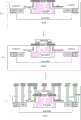
图1是本发明实施例的超高压SiGe HBT器件的结构示意图。FIG. 1 is a schematic structural view of an ultra-high voltage SiGe HBT device according to an embodiment of the present invention.
图2是本发明实施例的超高压SiGe HBT器件的制备工艺流程图。Fig. 2 is a flow chart of the preparation process of the ultra-high voltage SiGe HBT device of the embodiment of the present invention.
具体实施方式Detailed ways
为对本发明的技术内容、特点与功效有更具体的了解,现结合图示的实施方式,详述如下:In order to have a more specific understanding of the technical content, characteristics and effects of the present invention, now in conjunction with the illustrated embodiment, the details are as follows:
本实施例的超高压锗硅HBT晶体管器件的结构如图1所示,该结构的具体制备工艺步骤如下:The structure of the ultra-high voltage silicon germanium HBT transistor device of this embodiment is shown in Figure 1, and the specific preparation process steps of the structure are as follows:
步骤1,利用有源区光刻,在P型衬底上刻蚀出浅槽,然后分别利用N型和P型埋层的光罩进行埋层的注入,形成N埋层和P埋层,如图2(a)所示。Step 1: Etch a shallow groove on the P-type substrate by photolithography in the active area, and then use the masks of the N-type and P-type buried layers to implant the buried layer to form the N-buried layer and the P-buried layer, As shown in Figure 2(a).
其中,N埋层中注入的是磷或砷,注入的剂量范围为1E14~1E16cm-2,注入的能量范围为2~50KeV。P埋层中注入的是硼或氟化硼,注入的剂量范围为1E14~1E16cm-2,注入的能量范围2~30KeV。由于埋层离子注入能量较低,其与衬底的结面积较小,因此,埋层与衬底的寄生电容较小,不需要再采用深槽隔离技术。Wherein, phosphorous or arsenic is implanted into the N buried layer, the implanted dose ranges from 1E14 to 1E16 cm-2 , and the implanted energy ranges from 2 to 50 KeV. Boron or boron fluoride is implanted into the P buried layer, the implanted dose ranges from 1E14 to 1E16 cm-2 , and the implanted energy ranges from 2 to 30 KeV. Due to the low ion implantation energy of the buried layer, the junction area between the buried layer and the substrate is small, so the parasitic capacitance between the buried layer and the substrate is small, and no deep trench isolation technology is needed.
步骤2,依次淀积底部隔离介质氧化硅和掺杂多晶硅,然后进行化学机械研磨,将顶部的氧化硅磨平,露出多晶硅,接着进行多晶硅的刻蚀,将表面多晶硅刻除,如图2(b)所示。Step 2, sequentially deposit the bottom isolation dielectric silicon oxide and doped polysilicon, and then perform chemical mechanical polishing to smooth the top silicon oxide to expose the polysilicon, and then perform polysilicon etching to remove the surface polysilicon, as shown in Figure 2 ( b) as shown.
掺杂多晶硅可掺杂P型杂质(例如硼或氟化硼),也可掺杂N型杂质(例如磷或砷),杂质的体浓度为1.0E18~1.0E21 atoms/cm3。Doped polysilicon can be doped with P-type impurities (such as boron or boron fluoride), and can also be doped with N-type impurities (such as phosphorus or arsenic). The bulk concentration of impurities is 1.0E18-1.0E21 atoms/cm3 .
步骤3,进行多晶硅的过刻蚀,使得多晶硅的高度低于硅衬底表面,如图2(c)所示。Step 3, perform over-etching of the polysilicon, so that the height of the polysilicon is lower than the surface of the silicon substrate, as shown in FIG. 2(c).
步骤4,去除多晶硅上面的氧化硅,如图2(d)所示。Step 4, remove the silicon oxide on the polysilicon, as shown in Figure 2(d).
步骤5,通过光刻工艺,定义出多晶硅场板的位置,将不需要的多晶硅刻除,如图2(e)所示。In step 5, the position of the polysilicon field plate is defined through a photolithography process, and unnecessary polysilicon is etched away, as shown in FIG. 2(e).
步骤6,淀积氧化硅隔离介质层,将槽填满,使掺杂多晶硅埋于隔离介质层内部,见图2(f)中的浅沟槽隔离结构。Step 6, depositing a silicon oxide isolation dielectric layer, filling the trench, and burying doped polysilicon inside the isolation dielectric layer, see the shallow trench isolation structure in FIG. 2(f).
步骤7,通过腐蚀去除大部分有源区上的硬掩膜层,在两侧埋层之间的区域(包括有源区和部分场氧下区域)注入低剂量(1.0E11~1.0E13 atoms/cm2)的磷离子,其他HBT区域注入中剂量(1.0E13~1.0E15 atoms/cm2)的磷离子,形成集电区;然后淀积锗硅外延层,作为器件的基区,如图2(g)所示。Step 7, remove most of the hard mask layer on the active area by etching, and implant a low dose (1.0E11~1.0E13 atoms/ cm2 ) of phosphorus ions, and other HBT regions are implanted with phosphorus ions at a medium dose (1.0E13-1.0E15 atoms/cm2 ) to form a collector region; then a germanium-silicon epitaxial layer is deposited as the base region of the device, as shown in Figure 2 (g) shown.
步骤8,淀积氧化物介质层,打开发射区窗口后,淀积在位N型掺杂的多晶硅发射极,再注入N型杂质砷或磷,注入浓度要大于或等于2E15cm-2,注入能量由发射极厚度决定。然后光刻、刻蚀多晶硅,形成发射极和隔离介质层,如图2(h)所示。Step 8: Deposit an oxide dielectric layer. After opening the emitter window, deposit an in-situ N-type doped polysilicon emitter, and then implant N-type impurity arsenic or phosphorus. The implantation concentration must be greater than or equal to 2E15cm-2 , and the implantation energy Determined by emitter thickness. Then photolithography and etching polysilicon to form emitter and isolation dielectric layer, as shown in Figure 2(h).
步骤9,刻蚀深阱接触孔,在接触孔内生长过渡金属层Ti/TiN(钛/氮化钛),填入金属钨,并进行化学机械抛光,形成深阱接触孔,连接N埋层和P埋层,引出埋层所连接的集电区;该深阱接触孔距离器件很近,从而避免了过大的集电极电阻,也减小了集电极的寄生电容。同时,用传统的接触孔引出基区和发射区;集电区、基区和发射区的三个电极再使用金属引线引出,多晶硅场板和基区则通过金属引线连接在一起,如图2(i)所示。Step 9, etch the deep well contact hole, grow a transition metal layer Ti/TiN (titanium/titanium nitride) in the contact hole, fill in metal tungsten, and perform chemical mechanical polishing to form a deep well contact hole and connect the N buried layer and the P buried layer lead out the collector area connected to the buried layer; the deep well contact hole is very close to the device, thereby avoiding excessive collector resistance and reducing the parasitic capacitance of the collector. At the same time, the base area and the emitter area are drawn out with traditional contact holes; the three electrodes of the collector area, the base area, and the emitter area are drawn out with metal leads, and the polysilicon field plate and the base area are connected together through metal leads, as shown in Figure 2 (i) shown.
Claims (10)
Translated fromChinesePriority Applications (1)
| Application Number | Priority Date | Filing Date | Title |
|---|---|---|---|
| CN201110440342.1ACN102522425B (en) | 2011-12-23 | 2011-12-23 | Structure of ultrahigh pressure germanium-silicon heterojunction bipolar transistor (HBT) device and preparation method |
Applications Claiming Priority (1)
| Application Number | Priority Date | Filing Date | Title |
|---|---|---|---|
| CN201110440342.1ACN102522425B (en) | 2011-12-23 | 2011-12-23 | Structure of ultrahigh pressure germanium-silicon heterojunction bipolar transistor (HBT) device and preparation method |
Publications (2)
| Publication Number | Publication Date |
|---|---|
| CN102522425A CN102522425A (en) | 2012-06-27 |
| CN102522425Btrue CN102522425B (en) | 2014-04-16 |
Family
ID=46293282
Family Applications (1)
| Application Number | Title | Priority Date | Filing Date |
|---|---|---|---|
| CN201110440342.1AActiveCN102522425B (en) | 2011-12-23 | 2011-12-23 | Structure of ultrahigh pressure germanium-silicon heterojunction bipolar transistor (HBT) device and preparation method |
Country Status (1)
| Country | Link |
|---|---|
| CN (1) | CN102522425B (en) |
Cited By (3)
| Publication number | Priority date | Publication date | Assignee | Title |
|---|---|---|---|---|
| US10749017B1 (en) | 2019-02-12 | 2020-08-18 | Qualcomm Incorporated | Heterojunction bipolar transistors with field plates |
| WO2020209928A1 (en)* | 2019-04-10 | 2020-10-15 | Qualcomm Incorporated | Heterojunction bipolar transistor with field plates |
| EP3800669A1 (en)* | 2019-10-01 | 2021-04-07 | Analog Devices International Unlimited Company | A bipolar junction transistor, and a method of forming a charge control structure for a bipolar junction transistor |
Families Citing this family (8)
| Publication number | Priority date | Publication date | Assignee | Title |
|---|---|---|---|---|
| CN103681808A (en)* | 2012-09-09 | 2014-03-26 | 苏州英能电子科技有限公司 | LBJT (Lateral Bipolar Junction Transistor) containing field plate structure |
| EP2919272B1 (en)* | 2014-03-12 | 2020-05-27 | Nxp B.V. | Bipolar transistor device and method of fabrication |
| CN107887430A (en)* | 2017-11-09 | 2018-04-06 | 重庆邮电大学 | Substrate applies the silicon-germanium heterojunction bipolar transistor and its manufacture method of simple stress |
| US11563084B2 (en) | 2019-10-01 | 2023-01-24 | Analog Devices International Unlimited Company | Bipolar junction transistor, and a method of forming an emitter for a bipolar junction transistor |
| US11404540B2 (en) | 2019-10-01 | 2022-08-02 | Analog Devices International Unlimited Company | Bipolar junction transistor, and a method of forming a collector for a bipolar junction transistor |
| US11721719B2 (en)* | 2020-10-20 | 2023-08-08 | Globalfoundries U.S. Inc. | Heterojunction bipolar transistor with buried trap rich isolation region |
| CN115394838B (en)* | 2022-09-19 | 2025-08-08 | 华虹半导体(无锡)有限公司 | Method for manufacturing silicon-germanium heterojunction transistor |
| CN119967904B (en)* | 2025-04-10 | 2025-06-27 | 上海积塔半导体有限公司 | Semiconductor device and method of manufacturing the same |
Citations (5)
| Publication number | Priority date | Publication date | Assignee | Title |
|---|---|---|---|---|
| EP1646084A1 (en)* | 2004-10-06 | 2006-04-12 | Infineon Technologies AG | A method in the fabrication of an integrated injection logic circuit |
| CN101819994A (en)* | 2010-04-29 | 2010-09-01 | 上海宏力半导体制造有限公司 | Sige heterojunction bipolar transistor and preparation method thereof |
| EP2315238A1 (en)* | 2009-10-26 | 2011-04-27 | Nxp B.V. | Heterojunction Bipolar Transistor |
| CN102103997A (en)* | 2009-12-18 | 2011-06-22 | 上海华虹Nec电子有限公司 | Structure of groove type power MOS (Metal Oxide Semiconductor) device and preparation method thereof |
| CN102104062A (en)* | 2009-12-21 | 2011-06-22 | 上海华虹Nec电子有限公司 | Bipolar transistor |
Family Cites Families (1)
| Publication number | Priority date | Publication date | Assignee | Title |
|---|---|---|---|---|
| US6770952B2 (en)* | 2001-04-30 | 2004-08-03 | Texas Instruments Incorporated | Integrated process for high voltage and high performance silicon-on-insulator bipolar devices |
- 2011
- 2011-12-23CNCN201110440342.1Apatent/CN102522425B/enactiveActive
Patent Citations (5)
| Publication number | Priority date | Publication date | Assignee | Title |
|---|---|---|---|---|
| EP1646084A1 (en)* | 2004-10-06 | 2006-04-12 | Infineon Technologies AG | A method in the fabrication of an integrated injection logic circuit |
| EP2315238A1 (en)* | 2009-10-26 | 2011-04-27 | Nxp B.V. | Heterojunction Bipolar Transistor |
| CN102103997A (en)* | 2009-12-18 | 2011-06-22 | 上海华虹Nec电子有限公司 | Structure of groove type power MOS (Metal Oxide Semiconductor) device and preparation method thereof |
| CN102104062A (en)* | 2009-12-21 | 2011-06-22 | 上海华虹Nec电子有限公司 | Bipolar transistor |
| CN101819994A (en)* | 2010-04-29 | 2010-09-01 | 上海宏力半导体制造有限公司 | Sige heterojunction bipolar transistor and preparation method thereof |
Cited By (5)
| Publication number | Priority date | Publication date | Assignee | Title |
|---|---|---|---|---|
| US10749017B1 (en) | 2019-02-12 | 2020-08-18 | Qualcomm Incorporated | Heterojunction bipolar transistors with field plates |
| WO2020167363A1 (en)* | 2019-02-12 | 2020-08-20 | Qualcomm Incorporated | Heterojunction bipolar transistor with field plates |
| WO2020209928A1 (en)* | 2019-04-10 | 2020-10-15 | Qualcomm Incorporated | Heterojunction bipolar transistor with field plates |
| US11515406B2 (en) | 2019-04-10 | 2022-11-29 | Qualcomm Incorporated | Heterojunction bipolar transistor with field plates |
| EP3800669A1 (en)* | 2019-10-01 | 2021-04-07 | Analog Devices International Unlimited Company | A bipolar junction transistor, and a method of forming a charge control structure for a bipolar junction transistor |
Also Published As
| Publication number | Publication date |
|---|---|
| CN102522425A (en) | 2012-06-27 |
Similar Documents
| Publication | Publication Date | Title |
|---|---|---|
| CN102522425B (en) | Structure of ultrahigh pressure germanium-silicon heterojunction bipolar transistor (HBT) device and preparation method | |
| CN102437180B (en) | Ultra high voltage silicon germanium heterojunction bipolar transistor (HBT) device and manufacturing method thereof | |
| CN102403222B (en) | Manufacturing method for silicon germanium heterojunction bipolar transistors | |
| US20120098039A1 (en) | Sige heterojunction bipolar transistor having low collector/base capacitance and manufacturing method of the same | |
| CN102347354A (en) | Germanium-silicon heterojunction bipolar transistor and manufacturing method thereof | |
| CN108054203B (en) | Heterojunction bipolar transistor of silicon germanium substrate on insulator and manufacturing method thereof | |
| TW201801314A (en) | Heterojunction bipolar transistor with stress component | |
| US7554174B2 (en) | Bipolar transistor having semiconductor patterns filling contact windows of an insulating layer | |
| CN103066101B (en) | Germanium silicium HBT device and manufacture method | |
| CN103035690B (en) | Ultrahigh pressure germanium-silicon hetero-junction bipolar transistor and manufacturing method thereof | |
| US8866189B2 (en) | Silicon-germanium heterojunction bipolar transistor and manufacturing method thereof | |
| CN103117300B (en) | Parasitic lateral type PNP device and manufacture method | |
| CN102386218B (en) | Vertical parasitic PNP device in BiCMOS process and its manufacturing method | |
| CN102412275A (en) | Vertical PNP device in SiGe BiCMOS technology and manufacturing method thereof | |
| US9012279B2 (en) | SiGe HBT and method of manufacturing the same | |
| CN103050519B (en) | Germanium silicium HBT device and manufacture method | |
| US8785977B2 (en) | High speed SiGe HBT and manufacturing method thereof | |
| CN103050518B (en) | SiGe heterojunction bipolar transistor and manufacturing method thereof | |
| CN102412286B (en) | High speed SiGe HBT device structure and manufacture method thereof | |
| CN103035688B (en) | Germanium silicon heterojunction bipolar transistor (HBT) device and manufacturing method thereof | |
| CN113851526B (en) | Bipolar junction transistor and preparation method thereof | |
| CN103035748B (en) | Zener diode in germanium silicon BiCMOS technique and manufacture method | |
| CN103050520B (en) | SiGe HBT (Heterojunction Bipolar Transistor) apparatus and manufacturing method thereof | |
| CN103730354A (en) | Method for manufacturing germanium-silicon heterojunction bipolar transistor | |
| CN102916041B (en) | Germanium-silicon heterojunction bipolar transistor based on SOI (Silicon On Insulator) and manufacturing method thereof |
Legal Events
| Date | Code | Title | Description |
|---|---|---|---|
| C06 | Publication | ||
| PB01 | Publication | ||
| C10 | Entry into substantive examination | ||
| SE01 | Entry into force of request for substantive examination | ||
| ASS | Succession or assignment of patent right | Owner name:SHANGHAI HUAHONG GRACE SEMICONDUCTOR MANUFACTURING Free format text:FORMER OWNER: HUAHONG NEC ELECTRONICS CO LTD, SHANGHAI Effective date:20140107 | |
| C41 | Transfer of patent application or patent right or utility model | ||
| COR | Change of bibliographic data | Free format text:CORRECT: ADDRESS; FROM: 201206 PUDONG NEW AREA, SHANGHAI TO: 201203 PUDONG NEW AREA, SHANGHAI | |
| TA01 | Transfer of patent application right | Effective date of registration:20140107 Address after:201203 Shanghai city Zuchongzhi road Pudong New Area Zhangjiang hi tech Park No. 1399 Applicant after:Shanghai Huahong Grace Semiconductor Manufacturing Corporation Address before:201206, Shanghai, Pudong New Area, Sichuan Road, No. 1188 Bridge Applicant before:Shanghai Huahong NEC Electronics Co., Ltd. | |
| C14 | Grant of patent or utility model | ||
| GR01 | Patent grant |