CN102508411A - Method for producing X-ray diffraction optical element - Google Patents
Method for producing X-ray diffraction optical elementDownload PDFInfo
- Publication number
- CN102508411A CN102508411ACN2011103799934ACN201110379993ACN102508411ACN 102508411 ACN102508411 ACN 102508411ACN 2011103799934 ACN2011103799934 ACN 2011103799934ACN 201110379993 ACN201110379993 ACN 201110379993ACN 102508411 ACN102508411 ACN 102508411A
- Authority
- CN
- China
- Prior art keywords
- substrate
- ray diffraction
- optical element
- diffraction optical
- striated
- Prior art date
- Legal status (The legal status is an assumption and is not a legal conclusion. Google has not performed a legal analysis and makes no representation as to the accuracy of the status listed.)
- Pending
Links
- 230000003287optical effectEffects0.000titleclaimsabstractdescription38
- 238000002441X-ray diffractionMethods0.000titleclaimsabstractdescription27
- 238000004519manufacturing processMethods0.000titledescription5
- 239000000758substrateSubstances0.000claimsabstractdescription66
- 229920002120photoresistant polymerPolymers0.000claimsabstractdescription26
- 238000000034methodMethods0.000claimsabstractdescription21
- 239000007769metal materialSubstances0.000claimsabstractdescription13
- 238000002360preparation methodMethods0.000claimsabstractdescription9
- 238000000151depositionMethods0.000claimsabstractdescription4
- PXHVJJICTQNCMI-UHFFFAOYSA-NNickelChemical compound[Ni]PXHVJJICTQNCMI-UHFFFAOYSA-N0.000claimsdescription10
- 239000010931goldSubstances0.000claimsdescription8
- 238000010894electron beam technologyMethods0.000claimsdescription6
- PCHJSUWPFVWCPO-UHFFFAOYSA-NgoldChemical compound[Au]PCHJSUWPFVWCPO-UHFFFAOYSA-N0.000claimsdescription6
- 229910052737goldInorganic materials0.000claimsdescription6
- IJGRMHOSHXDMSA-UHFFFAOYSA-NAtomic nitrogenChemical compoundN#NIJGRMHOSHXDMSA-UHFFFAOYSA-N0.000claimsdescription5
- 239000004642PolyimideSubstances0.000claimsdescription5
- 229910052759nickelInorganic materials0.000claimsdescription5
- 229920001721polyimidePolymers0.000claimsdescription5
- 238000004528spin coatingMethods0.000claimsdescription5
- WFKWXMTUELFFGS-UHFFFAOYSA-NtungstenChemical compound[W]WFKWXMTUELFFGS-UHFFFAOYSA-N0.000claimsdescription5
- 229910052721tungstenInorganic materials0.000claimsdescription5
- 239000010937tungstenSubstances0.000claimsdescription5
- XUIMIQQOPSSXEZ-UHFFFAOYSA-NSiliconChemical compound[Si]XUIMIQQOPSSXEZ-UHFFFAOYSA-N0.000claimsdescription4
- 229910052710siliconInorganic materials0.000claimsdescription4
- 239000010703siliconSubstances0.000claimsdescription4
- 238000001459lithographyMethods0.000claimsdescription2
- 229910052757nitrogenInorganic materials0.000claimsdescription2
- 238000001039wet etchingMethods0.000claimsdescription2
- 238000007747platingMethods0.000claims3
- 230000008021depositionEffects0.000claims2
- 230000015572biosynthetic processEffects0.000claims1
- 238000005286illuminationMethods0.000claims1
- 239000002184metalSubstances0.000claims1
- 229910052751metalInorganic materials0.000claims1
- 238000000926separation methodMethods0.000claims1
- 230000000737periodic effectEffects0.000abstractdescription5
- 238000003825pressingMethods0.000abstractdescription2
- 238000009713electroplatingMethods0.000description10
- 238000005516engineering processMethods0.000description7
- 238000000609electron-beam lithographyMethods0.000description6
- 238000001704evaporationMethods0.000description6
- 230000009286beneficial effectEffects0.000description5
- VYPSYNLAJGMNEJ-UHFFFAOYSA-Nsilicon dioxideInorganic materialsO=[Si]=OVYPSYNLAJGMNEJ-UHFFFAOYSA-N0.000description4
- 239000003292glueSubstances0.000description3
- 238000010586diagramMethods0.000description2
- 238000005530etchingMethods0.000description2
- 230000008020evaporationEffects0.000description2
- 238000012986modificationMethods0.000description2
- 230000004048modificationEffects0.000description2
- 238000000206photolithographyMethods0.000description2
- 239000010453quartzSubstances0.000description2
- 238000004544sputter depositionMethods0.000description2
- 238000001015X-ray lithographyMethods0.000description1
- 229910001873dinitrogenInorganic materials0.000description1
- 230000000694effectsEffects0.000description1
- 239000000463materialSubstances0.000description1
- 238000004377microelectronicMethods0.000description1
- 238000005459micromachiningMethods0.000description1
- 230000005855radiationEffects0.000description1
Images


Landscapes
- Diffracting Gratings Or Hologram Optical Elements (AREA)
Abstract
Translated fromChinese
Description
Translated fromChinese技术领域technical field
本发明涉及微电子行业微加工及光学技术领域,尤其涉及一种X射线衍射光学元件的方法。The invention relates to the field of micromachining and optical technology in the microelectronics industry, in particular to a method for an X-ray diffraction optical element.
背景技术Background technique
随着衍射光学领域的发展,对于高密度光学元件的需求也越来越多,而传统的X射线衍射光学元器件的制备技术是采用电子束光刻和X射线光刻技术结合的方法制备X射线衍射光学元器件。由于电子束光刻成本高,周期长。X射线光刻伴有一定的辐射。这给实验人员带来的了一定的影响,并制约了X射线衍射光学元器件的大批量制作。此外,高密度的X射线衍射光学元件需要不断的重复光刻,传统的电子束光刻显然达不到要求。With the development of the field of diffractive optics, there are more and more demands for high-density optical components, while the traditional preparation technology of X-ray diffractive optical components is to prepare X Ray diffractive optics. Due to the high cost of electron beam lithography, the cycle time is long. X-ray lithography is accompanied by some radiation. This has a certain impact on the experimenters, and restricts the mass production of X-ray diffraction optical components. In addition, high-density X-ray diffractive optical elements require repeated lithography, and traditional electron beam lithography obviously cannot meet the requirements.
发明内容Contents of the invention
(一)要解决的技术问题(1) Technical problems to be solved
为解决上述的一个或多个问题,本发明提供了一种制备光学衍射元件的方法,以提高制备X射线衍射光学元件的效率。To solve one or more of the above problems, the present invention provides a method for manufacturing an optical diffraction element, so as to improve the efficiency of manufacturing an X-ray diffraction optical element.
(二)技术方案(2) Technical solutions
根据本发明的一个方面,提供了一种制备X射线衍射光学元件的方法。该方法包括:步骤A,制备掩模基片A,掩模基片A上具有图形占空比为1∶2n+1的分离的多个条纹状凸起,n≥1;步骤B,在纳米压印基底B旋涂感光光刻胶;步骤C,将掩模基片A具有条纹状凸起的一面压向纳米压印基底B上感光光刻胶的一面,采取紫外光光照固化,从而在感光光刻胶中形成第二条纹状凹槽;步骤D,移除掩模基片A;步骤F,在第二条纹状凹槽内沉积第二金属材料;步骤G,再执行n次步骤B至步骤F,并且每次执行步骤C时,掩模基片A上条纹状凸起与前一次的第二条纹状凹槽之间的水平间隔与条纹状凸起的宽度相同;步骤H,去除纳米压印基底B上的感光光刻胶,从而形成图形占空比为1∶1的X射线衍射光学元件。According to one aspect of the present invention, a method for preparing an X-ray diffraction optical element is provided. The method comprises: step A, preparing a mask substrate A, on which there are a plurality of striped protrusions with a pattern duty ratio of 1:2n+1, n≥1; step B, in the nano The imprinting substrate B is spin-coated with photoresist; step C, pressing the side of the mask substrate A with stripe-shaped protrusions to the side of the photoresist on the nanoimprinting substrate B, and curing with ultraviolet light, so that the Forming a second striped groove in the photosensitive photoresist; step D, removing the mask substrate A; step F, depositing a second metal material in the second striped groove; step G, performing step B again n times To step F, and each time step C is performed, the horizontal interval between the striped protrusion on the mask substrate A and the previous second striped groove is the same as the width of the striped protrusion; step H, remove The photosensitive photoresist on the substrate B is nano-imprinted to form an X-ray diffraction optical element with a pattern duty ratio of 1:1.
(三)有益效果(3) Beneficial effects
本发明制备光学衍射元件的方法具备以下有益效果:The method for preparing an optical diffraction element of the present invention has the following beneficial effects:
1、本发明将传统的周期性光栅分成多步进行操作,在此情况下,不同于周期性的光栅,电子束光刻的精度可以达到更高,而且有较好的高宽比,而后期通过多次纳米压印,弥补了线宽比不等的情况,从而满足线宽比为1∶1的要求;1. The present invention divides the traditional periodic grating into multi-step operations. In this case, unlike the periodic grating, the precision of electron beam lithography can be higher and has a better aspect ratio. Through multiple nanoimprints, the situation of unequal line width ratio is made up, so as to meet the requirement of line width ratio of 1:1;
3、相对于传统的制备技术,利用纳米压印的效率高,能实现高效率,低成本,无辐射的X射线衍射光学元件的制备;并且,利用电子束光刻的高精度,可以制备出高精度的X射线衍射光学元器件。3. Compared with the traditional preparation technology, the use of nanoimprinting has high efficiency, and can realize the preparation of high-efficiency, low-cost, and radiation-free X-ray diffraction optical elements; and, using the high precision of electron beam lithography, it is possible to prepare High-precision X-ray diffraction optical components.
以上所述的具体实施例,对本发明的目的、技术方案和有益效果进行了进一步详细说明,所应理解的是,以上所述仅为本发明的具体实施例而已,并不用于限制本发明,凡在本发明的精神和原则之内,所做的任何修改、等同替换、改进等,均应包含在本发明的保护范围之内。The specific embodiments described above have further described the purpose, technical solutions and beneficial effects of the present invention in detail. It should be understood that the above descriptions are only specific embodiments of the present invention and are not intended to limit the present invention. Any modifications, equivalent replacements, improvements, etc. made within the spirit and principles of the present invention shall be included within the protection scope of the present invention.
附图说明Description of drawings
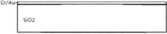
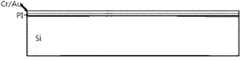
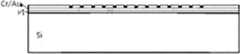
图1A-图1H本发明实施例制备衍射光学元件方法中执行各步骤后的元件结构示意图。FIG. 1A-FIG. 1H are schematic diagrams of the element structure after performing various steps in the method for preparing a diffractive optical element according to an embodiment of the present invention.
具体实施方式Detailed ways
为使本发明的目的、技术方案和优点更加清楚明白,以下结合具体实施例,并参照附图,对本发明进一步详细说明。此外,虽然本文可提供包含特定值的参数的示范,但应了解,参数无需确切等于相应的值,而是可在可接受的误差容限或设计约束内近似于所述值。In order to make the object, technical solution and advantages of the present invention clearer, the present invention will be described in further detail below in conjunction with specific embodiments and with reference to the accompanying drawings. Furthermore, while illustrations of parameters comprising particular values may be provided herein, it should be understood that the parameters need not be exactly equal to the respective values, but rather can be approximated within acceptable error margins or design constraints.
随着纳米压印技术的发展,其成本逐步降低,精确度逐步提高,从而为制备高密度X射线衍射光学元件提供了一个很好的借鉴平台。本发明正是依赖于上述的思路而产生的。With the development of nanoimprint technology, its cost is gradually reduced and its accuracy is gradually improved, which provides a good reference platform for the preparation of high-density X-ray diffraction optical elements. The present invention just relies on above-mentioned thinking and produces.
在本发明的一个示例性实施例中,提供了一种制备衍射光学元件的方法。图1A-图1H本发明实施例制备衍射光学元件方法中执行各步骤后的元件结构示意图。假设待制备的衍射光学元件两线条之间的线宽H1为10nm,则本实施例包括:In an exemplary embodiment of the present invention, a method of manufacturing a diffractive optical element is provided. FIG. 1A-FIG. 1H are schematic diagrams of the element structure after performing various steps in the method for preparing a diffractive optical element according to an embodiment of the present invention. Assuming that the line width H1 between the two lines of the diffractive optical element to be prepared is 10nm, this embodiment includes:
步骤S102,在光滑的石英片上蒸发一层Cr/Au层作为电镀种子层,作为纳米压印的掩模基片A,如图1A所示;Step S102, evaporating a Cr/Au layer on a smooth quartz sheet as an electroplating seed layer, as a mask substrate A for nanoimprinting, as shown in Figure 1A;
本步骤中,掩膜基片A的衬底也可以采用除石英片之外的其他硬质材料,只要能够满足了纳米压印技术对掩模的硬度要求即可。此外,由于后期采用电镀方式进行掩模基片中金属材质条纹状凸起,因此,在本步骤中沉积了一层电镀种子层。如果后期采用蒸发或溅射等方式进行金属材质条纹状凸起的制备,该蒸发电镀种子层的步骤也可以省略。In this step, the substrate of the mask substrate A may also be made of hard materials other than the quartz sheet, as long as the hardness requirements of the nanoimprint technology for the mask can be met. In addition, because electroplating is used in the later stage to form the striped protrusions of the metal material in the mask substrate, a layer of electroplating seed layer is deposited in this step. If evaporation or sputtering is used to prepare the striped protrusions of metal material in the later stage, the step of evaporating and electroplating the seed layer can also be omitted.
步骤S104,在电镀种子层上旋涂一层电子束光刻胶,厚度为600nm-700nm,利用电子束进行光刻,显影后形成占空比为1∶(2n+1)的条纹状凹槽,如图1B所示,n≥1;Step S104, spin-coat a layer of electron beam photoresist on the electroplating seed layer with a thickness of 600nm-700nm, conduct photolithography with electron beam, and form striped grooves with a duty ratio of 1:(2n+1) after development , as shown in Figure 1B, n≥1;
本步骤中,n为大于等于1的整数。该n与后期纳米压印的次数有关,将在后续步骤中详细描述。每一条条纹状凹槽的宽度为a。In this step, n is an integer greater than or equal to 1. The n is related to the number of nanoimprints in the later stage, which will be described in detail in the subsequent steps. The width of each striped groove is a.
步骤S106,刻蚀条纹状凹槽底部残余的胶,并刻蚀电极,在条纹状凹槽内电镀第一金属材料(镍、金或者钨);Step S106, etching the remaining glue at the bottom of the striped groove, etching the electrodes, and electroplating the first metal material (nickel, gold or tungsten) in the striped groove;
步骤S108,去除掩模基片A的衬底上的光刻胶,露出其上方由所述第一金属材料形成的条纹状凸起,形成所需的掩模基片A,如图1C所示。Step S108, removing the photoresist on the substrate of the mask substrate A, exposing the striped protrusions formed by the first metal material above it, and forming the required mask substrate A, as shown in FIG. 1C .
步骤S110,在光滑的硅片上旋涂一层聚酰亚胺,形成支撑薄膜,然后蒸发一层Cr/Au层作为电镀种子层,作为纳米压印基底B,如图1D所示;Step S110, spin-coating a layer of polyimide on a smooth silicon wafer to form a support film, and then evaporating a layer of Cr/Au as an electroplating seed layer as a nanoimprint substrate B, as shown in Figure 1D;
同步骤S102类似,在本步骤中沉积了一层电镀种子层。如果后期采用蒸发或溅射等方式进行金属材质条纹状凸起的制备,该蒸发电镀种子层的步骤可以省略。Similar to step S102, an electroplating seed layer is deposited in this step. If evaporation or sputtering is used to prepare the stripe-shaped projections of metal material later, the step of evaporating and electroplating the seed layer can be omitted.
步骤S112,在纳米压印基底B上旋涂一层感光光刻胶,厚度为400nm-500nm;Step S112, spin-coating a layer of photosensitive photoresist on the nanoimprint substrate B with a thickness of 400nm-500nm;
可以看出,在纳米压印基底B上旋涂感光光刻胶的厚度要小于掩模基片A的光刻胶厚度,从而掩模制作完成的镍、金或者钨的厚度比基底的光刻胶厚度大,从而基底上的光刻胶不会影响掩模基片。It can be seen that the thickness of the spin-coated photosensitive photoresist on the nanoimprint substrate B is smaller than the thickness of the photoresist on the mask substrate A, so that the thickness of the finished nickel, gold or tungsten mask is smaller than that of the photoresist on the substrate. The glue thickness is large so that the photoresist on the substrate does not affect the mask substrate.
步骤S114,将掩模基片A置于在纳米压印基底B上,施加一定的压力,用UV光照固化,固化的参数:温度范围从室温到350摄氏度;压力范围从5到20个PSI;真空范围从1个标准大气压到0.1帕;时间约为0.3s。如图1E所示。Step S114, placing the mask substrate A on the nanoimprint substrate B, applying a certain pressure, and curing with UV light. The curing parameters: the temperature ranges from room temperature to 350 degrees Celsius; the pressure ranges from 5 to 20 PSI; The vacuum range is from 1 standard atmosphere to 0.1 Pa; the time is about 0.3s. As shown in Figure 1E.
使用的UV紫外光固化技术是在常温常压下进行,不需要进行高温。The UV ultraviolet curing technology used is carried out at normal temperature and pressure, and does not require high temperature.
步骤S116,然后在纳米压印基底B和掩模基片A中间缓慢通入氮气,并固定其平行方向,使得掩模基片A向上移除;Step S116, then slowly inject nitrogen into the middle of the nanoimprint substrate B and the mask substrate A, and fix the parallel direction, so that the mask substrate A is removed upward;
刻蚀基底上的残余光刻胶,并刻蚀电极,然后进行电镀镍、金或者钨,从而形成光栅的一部分凸起,如图1F所示。The residual photoresist on the substrate is etched, and the electrodes are etched, and then electroplated with nickel, gold or tungsten to form a part of the grating protrusion, as shown in FIG. 1F .
步骤S118,在光刻后,将掩模基片A和纳米压印基底B分开是在掩模基片A和纳米压印基底B间通入氮气,从而使其自动分开,消除了机械移动对图形的影响。In step S118, after the photolithography, the mask substrate A and the nanoimprint substrate B are separated by passing nitrogen gas between the mask substrate A and the nanoimprint substrate B, so that they are separated automatically, eliminating the need for mechanical movement. Graphical effects.
步骤S120,重复在纳米压印基片B上匀胶和纳米压印以及电镀步骤,每次压印的位置与上一次的位置向右移,直至纳米压印基底B上的线条和空隙宽度全部一样。此次掩模基片A的线条与先前的线条之间间隔等于掩模基片A的线条,如图1G所示;Step S120, repeating the steps of distributing glue, nanoimprinting and electroplating on the nanoimprinting substrate B, and moving the position of each imprinting to the right from the previous position until the width of the lines and gaps on the nanoimprinting substrate B are all Same. The distance between the lines of the mask substrate A and the previous lines is equal to the lines of the mask substrate A, as shown in FIG. 1G;
本领域技术人员应当了解,本实施例中自左向右逐次压印,当然也可以自右向左逐次压印,只是为了保证压印的精度,保证压印的顺序始终朝向一个方向即可。Those skilled in the art should understand that in this embodiment, stamping is performed sequentially from left to right, of course, stamping can also be performed sequentially from right to left, just to ensure the accuracy of stamping and ensure that the stamping sequence always faces one direction.
步骤S122,去除纳米压印基底B上的感光光刻胶,,形成图形占空比为1∶1的X射线衍射光学元件;Step S122, removing the photosensitive photoresist on the nanoimprint substrate B to form an X-ray diffraction optical element with a pattern duty ratio of 1:1;
步骤S124,湿法腐蚀纳米压印基底B背面的硅,刻蚀底金,完成最终器件,如图1H所示。Step S124 , wet etching the silicon on the back of the nanoimprint substrate B to etch the bottom gold to complete the final device, as shown in FIG. 1H .
从上述实施例可以看出,本发明制备光学衍射元件的方法具备以下有益效果:As can be seen from the foregoing embodiments, the method for preparing an optical diffraction element of the present invention has the following beneficial effects:
1、本发明将传统的周期性光栅分成多步进行操作,在此情况下,不同于周期性的光栅,电子束光刻的精度可以达到更高,而且有较好的高宽比,而后期通过多次纳米压印,弥补了线宽比不等的情况,从而满足线宽比为1∶1的要求;1. The present invention divides the traditional periodic grating into multi-step operations. In this case, unlike the periodic grating, the precision of electron beam lithography can be higher and has a better aspect ratio. Through multiple nanoimprints, the situation of unequal line width ratio is made up, so as to meet the requirement of line width ratio of 1:1;
3、相对于传统的制备技术,利用纳米压印的效率高,能实现高效率,低成本,无辐射的X射线衍射光学元件的制备;并且,利用电子束光刻的高精度,可以制备出高精度的X射线衍射光学元器件。3. Compared with the traditional preparation technology, the use of nanoimprinting has high efficiency, and can realize the preparation of high-efficiency, low-cost, and radiation-free X-ray diffraction optical elements; and, using the high precision of electron beam lithography, it is possible to prepare High-precision X-ray diffraction optical components.
以上所述的具体实施例,对本发明的目的、技术方案和有益效果进行了进一步详细说明,所应理解的是,以上所述仅为本发明的具体实施例而已,并不用于限制本发明,凡在本发明的精神和原则之内,所做的任何修改、等同替换、改进等,均应包含在本发明的保护范围之内。The specific embodiments described above have further described the purpose, technical solutions and beneficial effects of the present invention in detail. It should be understood that the above descriptions are only specific embodiments of the present invention and are not intended to limit the present invention. Any modifications, equivalent replacements, improvements, etc. made within the spirit and principles of the present invention shall be included within the protection scope of the present invention.
Claims (10)
Priority Applications (1)
| Application Number | Priority Date | Filing Date | Title |
|---|---|---|---|
| CN2011103799934ACN102508411A (en) | 2011-11-25 | 2011-11-25 | Method for producing X-ray diffraction optical element |
Applications Claiming Priority (1)
| Application Number | Priority Date | Filing Date | Title |
|---|---|---|---|
| CN2011103799934ACN102508411A (en) | 2011-11-25 | 2011-11-25 | Method for producing X-ray diffraction optical element |
Publications (1)
| Publication Number | Publication Date |
|---|---|
| CN102508411Atrue CN102508411A (en) | 2012-06-20 |
Family
ID=46220513
Family Applications (1)
| Application Number | Title | Priority Date | Filing Date |
|---|---|---|---|
| CN2011103799934APendingCN102508411A (en) | 2011-11-25 | 2011-11-25 | Method for producing X-ray diffraction optical element |
Country Status (1)
| Country | Link |
|---|---|
| CN (1) | CN102508411A (en) |
Cited By (5)
| Publication number | Priority date | Publication date | Assignee | Title |
|---|---|---|---|---|
| CN103969941A (en)* | 2014-05-26 | 2014-08-06 | 苏州大学 | Mask as well as preparation method and graphing method thereof |
| CN107219579A (en)* | 2017-07-10 | 2017-09-29 | 扬州大学 | The groove-shaped cycle grating array preparation method of multiple frequence |
| CN107356997A (en)* | 2017-07-10 | 2017-11-17 | 扬州大学 | Multiple frequence grizzly bar type cycle grating array preparation method |
| CN109801733A (en)* | 2018-12-29 | 2019-05-24 | 深圳大学 | X-ray absorption preparing grating method and its X-ray absorption grating |
| CN114296168A (en)* | 2021-12-08 | 2022-04-08 | 中国科学技术大学 | A method for fabricating variable-period narrow gratings using a wide-grating nanoimprint template |
Citations (9)
| Publication number | Priority date | Publication date | Assignee | Title |
|---|---|---|---|---|
| CN101001001A (en)* | 2006-12-20 | 2007-07-18 | 武汉光迅科技股份有限公司 | Manufacturing method of low cost DFB laser |
| CN101017214A (en)* | 2006-02-08 | 2007-08-15 | 中国科学院微电子研究所 | Manufacturing method of high-resolution self-supporting full-hollowed-out transmission grating |
| JP2008049544A (en)* | 2006-08-23 | 2008-03-06 | Nippon Sheet Glass Co Ltd | Nano-imprinting method and nano-imprinting apparatus |
| CN101261331A (en)* | 2008-04-21 | 2008-09-10 | 南京大学 | Self-supporting transmission metal grating based on nanoimprint technology and its preparation method |
| CN101446759A (en)* | 2008-12-24 | 2009-06-03 | 武汉光迅科技股份有限公司 | Method for producing secondary coining moulding board for nanometer coining and secondary coining moulding board thereof |
| CN101520600A (en)* | 2008-02-27 | 2009-09-02 | 中国科学院微电子研究所 | Method for making light-transmitting nanoimprint template based on X-ray exposure technology |
| CN201331670Y (en)* | 2008-12-24 | 2009-10-21 | 武汉光迅科技股份有限公司 | Secondary imprint template for nanometer imprint |
| JP2011181704A (en)* | 2010-03-01 | 2011-09-15 | Osaka Prefecture Univ | Method of manufacturing fine structure using solvent dissolving type optical curing composition |
| CN102402118A (en)* | 2011-11-25 | 2012-04-04 | 中国科学院微电子研究所 | Method for producing X-ray diffraction optical element |
- 2011
- 2011-11-25CNCN2011103799934Apatent/CN102508411A/enactivePending
Patent Citations (9)
| Publication number | Priority date | Publication date | Assignee | Title |
|---|---|---|---|---|
| CN101017214A (en)* | 2006-02-08 | 2007-08-15 | 中国科学院微电子研究所 | Manufacturing method of high-resolution self-supporting full-hollowed-out transmission grating |
| JP2008049544A (en)* | 2006-08-23 | 2008-03-06 | Nippon Sheet Glass Co Ltd | Nano-imprinting method and nano-imprinting apparatus |
| CN101001001A (en)* | 2006-12-20 | 2007-07-18 | 武汉光迅科技股份有限公司 | Manufacturing method of low cost DFB laser |
| CN101520600A (en)* | 2008-02-27 | 2009-09-02 | 中国科学院微电子研究所 | Method for making light-transmitting nanoimprint template based on X-ray exposure technology |
| CN101261331A (en)* | 2008-04-21 | 2008-09-10 | 南京大学 | Self-supporting transmission metal grating based on nanoimprint technology and its preparation method |
| CN101446759A (en)* | 2008-12-24 | 2009-06-03 | 武汉光迅科技股份有限公司 | Method for producing secondary coining moulding board for nanometer coining and secondary coining moulding board thereof |
| CN201331670Y (en)* | 2008-12-24 | 2009-10-21 | 武汉光迅科技股份有限公司 | Secondary imprint template for nanometer imprint |
| JP2011181704A (en)* | 2010-03-01 | 2011-09-15 | Osaka Prefecture Univ | Method of manufacturing fine structure using solvent dissolving type optical curing composition |
| CN102402118A (en)* | 2011-11-25 | 2012-04-04 | 中国科学院微电子研究所 | Method for producing X-ray diffraction optical element |
Non-Patent Citations (1)
| Title |
|---|
| 范东升等: "纳米压印光刻模版制作技术", 《电子工业专用设备》, no. 121, 28 February 2005 (2005-02-28)* |
Cited By (7)
| Publication number | Priority date | Publication date | Assignee | Title |
|---|---|---|---|---|
| CN103969941A (en)* | 2014-05-26 | 2014-08-06 | 苏州大学 | Mask as well as preparation method and graphing method thereof |
| CN107219579A (en)* | 2017-07-10 | 2017-09-29 | 扬州大学 | The groove-shaped cycle grating array preparation method of multiple frequence |
| CN107356997A (en)* | 2017-07-10 | 2017-11-17 | 扬州大学 | Multiple frequence grizzly bar type cycle grating array preparation method |
| CN109801733A (en)* | 2018-12-29 | 2019-05-24 | 深圳大学 | X-ray absorption preparing grating method and its X-ray absorption grating |
| CN109801733B (en)* | 2018-12-29 | 2020-10-27 | 深圳大学 | Manufacturing method of X-ray absorption grating and X-ray absorption grating |
| CN114296168A (en)* | 2021-12-08 | 2022-04-08 | 中国科学技术大学 | A method for fabricating variable-period narrow gratings using a wide-grating nanoimprint template |
| CN114296168B (en)* | 2021-12-08 | 2023-03-10 | 中国科学技术大学 | A method of fabricating variable-period narrow gratings using wide grating nanoimprint templates |
Similar Documents
| Publication | Publication Date | Title |
|---|---|---|
| JP5274128B2 (en) | Imprint method and substrate processing method | |
| TWI628516B (en) | Nano imprinting with reusable polymer template with metallic or oxide coating | |
| CN101520600B (en) | Method for manufacturing light-transmitting nano-imprint template based on X-ray exposure technology | |
| US20100167181A1 (en) | Photomask for Extreme Ultraviolet Lithography and Method for Fabricating the Same | |
| US20070176320A1 (en) | Mold for imprint, process for producing minute structure using the mold, and process for producing the mold | |
| US10151041B2 (en) | Manufacturing method of metal mask and mask for deposition using said method | |
| JP4407770B2 (en) | Pattern formation method | |
| JP2005203797A (en) | Fabricating method of large area stamp for nanoimprint lithography | |
| US20080149488A1 (en) | Solvent-soluble stamp for nano-imprint lithography and method of manufacturing the same | |
| US10288999B2 (en) | Methods for controlling extrusions during imprint template replication processes | |
| CN102508411A (en) | Method for producing X-ray diffraction optical element | |
| KR20120067170A (en) | Method of manufacturing stamp for nanoimprint | |
| CN107121890A (en) | A kind of nano-imprint stamp and preparation method thereof | |
| JP2013543456A (en) | High contrast alignment mark by multi-stage imprint | |
| CN102466980A (en) | Method for fabricating multilayer blazed gratings based on electron beam lithography and X-ray exposure | |
| CN111752090B (en) | Imprint mold manufacturing method | |
| TWI650619B (en) | Method for preparing grating | |
| CN102289015A (en) | Method for manufacturing X-ray diffraction grating with large height-width ratio | |
| CN114460819B (en) | Alignment mark for electron beam exposure and preparation method thereof | |
| CN109212898A (en) | A kind of nano-imprint stamp and preparation method thereof | |
| JP2013193454A (en) | Method of manufacturing master mold, method of manufacturing mold, and surface processing method used for them | |
| US11261085B2 (en) | Methods for micro and nano fabrication by selective template removal | |
| JP2022522424A (en) | Methods and equipment for stamp generation and curing | |
| CN103116242B (en) | A Method for Fabricating Heterostructures Without Alignment Nanoimprinting | |
| CN108550527B (en) | Graphical method |
Legal Events
| Date | Code | Title | Description |
|---|---|---|---|
| C06 | Publication | ||
| PB01 | Publication | ||
| C10 | Entry into substantive examination | ||
| SE01 | Entry into force of request for substantive examination | ||
| C02 | Deemed withdrawal of patent application after publication (patent law 2001) | ||
| WD01 | Invention patent application deemed withdrawn after publication | Application publication date:20120620 |