CN102498553A - Transistor and display device - Google Patents
Transistor and display deviceDownload PDFInfo
- Publication number
- CN102498553A CN102498553ACN2010800412321ACN201080041232ACN102498553ACN 102498553 ACN102498553 ACN 102498553ACN 2010800412321 ACN2010800412321 ACN 2010800412321ACN 201080041232 ACN201080041232 ACN 201080041232ACN 102498553 ACN102498553 ACN 102498553A
- Authority
- CN
- China
- Prior art keywords
- layer
- transistor
- oxide semiconductor
- semiconductor layer
- electrode layer
- Prior art date
- Legal status (The legal status is an assumption and is not a legal conclusion. Google has not performed a legal analysis and makes no representation as to the accuracy of the status listed.)
- Granted
Links
Images


Classifications
- H—ELECTRICITY
- H10—SEMICONDUCTOR DEVICES; ELECTRIC SOLID-STATE DEVICES NOT OTHERWISE PROVIDED FOR
- H10D—INORGANIC ELECTRIC SEMICONDUCTOR DEVICES
- H10D30/00—Field-effect transistors [FET]
- H10D30/60—Insulated-gate field-effect transistors [IGFET]
- H10D30/67—Thin-film transistors [TFT]
- H—ELECTRICITY
- H10—SEMICONDUCTOR DEVICES; ELECTRIC SOLID-STATE DEVICES NOT OTHERWISE PROVIDED FOR
- H10D—INORGANIC ELECTRIC SEMICONDUCTOR DEVICES
- H10D30/00—Field-effect transistors [FET]
- H10D30/60—Insulated-gate field-effect transistors [IGFET]
- H10D30/67—Thin-film transistors [TFT]
- H10D30/674—Thin-film transistors [TFT] characterised by the active materials
- H10D30/6755—Oxide semiconductors, e.g. zinc oxide, copper aluminium oxide or cadmium stannate
- G—PHYSICS
- G02—OPTICS
- G02F—OPTICAL DEVICES OR ARRANGEMENTS FOR THE CONTROL OF LIGHT BY MODIFICATION OF THE OPTICAL PROPERTIES OF THE MEDIA OF THE ELEMENTS INVOLVED THEREIN; NON-LINEAR OPTICS; FREQUENCY-CHANGING OF LIGHT; OPTICAL LOGIC ELEMENTS; OPTICAL ANALOGUE/DIGITAL CONVERTERS
- G02F1/00—Devices or arrangements for the control of the intensity, colour, phase, polarisation or direction of light arriving from an independent light source, e.g. switching, gating or modulating; Non-linear optics
- G02F1/01—Devices or arrangements for the control of the intensity, colour, phase, polarisation or direction of light arriving from an independent light source, e.g. switching, gating or modulating; Non-linear optics for the control of the intensity, phase, polarisation or colour
- G02F1/13—Devices or arrangements for the control of the intensity, colour, phase, polarisation or direction of light arriving from an independent light source, e.g. switching, gating or modulating; Non-linear optics for the control of the intensity, phase, polarisation or colour based on liquid crystals, e.g. single liquid crystal display cells
- G02F1/133—Constructional arrangements; Operation of liquid crystal cells; Circuit arrangements
- G02F1/136—Liquid crystal cells structurally associated with a semi-conducting layer or substrate, e.g. cells forming part of an integrated circuit
- G02F1/1362—Active matrix addressed cells
- H—ELECTRICITY
- H10—SEMICONDUCTOR DEVICES; ELECTRIC SOLID-STATE DEVICES NOT OTHERWISE PROVIDED FOR
- H10D—INORGANIC ELECTRIC SEMICONDUCTOR DEVICES
- H10D30/00—Field-effect transistors [FET]
- H10D30/60—Insulated-gate field-effect transistors [IGFET]
- H10D30/67—Thin-film transistors [TFT]
- H10D30/6704—Thin-film transistors [TFT] having supplementary regions or layers in the thin films or in the insulated bulk substrates for controlling properties of the device
- H10D30/6713—Thin-film transistors [TFT] having supplementary regions or layers in the thin films or in the insulated bulk substrates for controlling properties of the device characterised by the properties of the source or drain regions, e.g. compositions or sectional shapes
- H—ELECTRICITY
- H10—SEMICONDUCTOR DEVICES; ELECTRIC SOLID-STATE DEVICES NOT OTHERWISE PROVIDED FOR
- H10D—INORGANIC ELECTRIC SEMICONDUCTOR DEVICES
- H10D30/00—Field-effect transistors [FET]
- H10D30/60—Insulated-gate field-effect transistors [IGFET]
- H10D30/67—Thin-film transistors [TFT]
- H10D30/674—Thin-film transistors [TFT] characterised by the active materials
- H10D30/6755—Oxide semiconductors, e.g. zinc oxide, copper aluminium oxide or cadmium stannate
- H10D30/6756—Amorphous oxide semiconductors
- H—ELECTRICITY
- H10—SEMICONDUCTOR DEVICES; ELECTRIC SOLID-STATE DEVICES NOT OTHERWISE PROVIDED FOR
- H10D—INORGANIC ELECTRIC SEMICONDUCTOR DEVICES
- H10D30/00—Field-effect transistors [FET]
- H10D30/60—Insulated-gate field-effect transistors [IGFET]
- H10D30/67—Thin-film transistors [TFT]
- H10D30/6757—Thin-film transistors [TFT] characterised by the structure of the channel, e.g. transverse or longitudinal shape or doping profile
- H—ELECTRICITY
- H10—SEMICONDUCTOR DEVICES; ELECTRIC SOLID-STATE DEVICES NOT OTHERWISE PROVIDED FOR
- H10D—INORGANIC ELECTRIC SEMICONDUCTOR DEVICES
- H10D62/00—Semiconductor bodies, or regions thereof, of devices having potential barriers
- H10D62/10—Shapes, relative sizes or dispositions of the regions of the semiconductor bodies; Shapes of the semiconductor bodies
- H—ELECTRICITY
- H10—SEMICONDUCTOR DEVICES; ELECTRIC SOLID-STATE DEVICES NOT OTHERWISE PROVIDED FOR
- H10D—INORGANIC ELECTRIC SEMICONDUCTOR DEVICES
- H10D62/00—Semiconductor bodies, or regions thereof, of devices having potential barriers
- H10D62/40—Crystalline structures
- H—ELECTRICITY
- H10—SEMICONDUCTOR DEVICES; ELECTRIC SOLID-STATE DEVICES NOT OTHERWISE PROVIDED FOR
- H10D—INORGANIC ELECTRIC SEMICONDUCTOR DEVICES
- H10D62/00—Semiconductor bodies, or regions thereof, of devices having potential barriers
- H10D62/40—Crystalline structures
- H10D62/405—Orientations of crystalline planes
- H—ELECTRICITY
- H10—SEMICONDUCTOR DEVICES; ELECTRIC SOLID-STATE DEVICES NOT OTHERWISE PROVIDED FOR
- H10D—INORGANIC ELECTRIC SEMICONDUCTOR DEVICES
- H10D86/00—Integrated devices formed in or on insulating or conducting substrates, e.g. formed in silicon-on-insulator [SOI] substrates or on stainless steel or glass substrates
- H10D86/40—Integrated devices formed in or on insulating or conducting substrates, e.g. formed in silicon-on-insulator [SOI] substrates or on stainless steel or glass substrates characterised by multiple TFTs
- H10D86/421—Integrated devices formed in or on insulating or conducting substrates, e.g. formed in silicon-on-insulator [SOI] substrates or on stainless steel or glass substrates characterised by multiple TFTs having a particular composition, shape or crystalline structure of the active layer
- H10D86/423—Integrated devices formed in or on insulating or conducting substrates, e.g. formed in silicon-on-insulator [SOI] substrates or on stainless steel or glass substrates characterised by multiple TFTs having a particular composition, shape or crystalline structure of the active layer comprising semiconductor materials not belonging to the Group IV, e.g. InGaZnO
- H—ELECTRICITY
- H10—SEMICONDUCTOR DEVICES; ELECTRIC SOLID-STATE DEVICES NOT OTHERWISE PROVIDED FOR
- H10D—INORGANIC ELECTRIC SEMICONDUCTOR DEVICES
- H10D86/00—Integrated devices formed in or on insulating or conducting substrates, e.g. formed in silicon-on-insulator [SOI] substrates or on stainless steel or glass substrates
- H10D86/40—Integrated devices formed in or on insulating or conducting substrates, e.g. formed in silicon-on-insulator [SOI] substrates or on stainless steel or glass substrates characterised by multiple TFTs
- H10D86/60—Integrated devices formed in or on insulating or conducting substrates, e.g. formed in silicon-on-insulator [SOI] substrates or on stainless steel or glass substrates characterised by multiple TFTs wherein the TFTs are in active matrices
- H—ELECTRICITY
- H10—SEMICONDUCTOR DEVICES; ELECTRIC SOLID-STATE DEVICES NOT OTHERWISE PROVIDED FOR
- H10K—ORGANIC ELECTRIC SOLID-STATE DEVICES
- H10K59/00—Integrated devices, or assemblies of multiple devices, comprising at least one organic light-emitting element covered by group H10K50/00
Landscapes
- Physics & Mathematics (AREA)
- Nonlinear Science (AREA)
- Chemical & Material Sciences (AREA)
- Crystallography & Structural Chemistry (AREA)
- Engineering & Computer Science (AREA)
- Microelectronics & Electronic Packaging (AREA)
- Mathematical Physics (AREA)
- General Physics & Mathematics (AREA)
- Optics & Photonics (AREA)
- Thin Film Transistor (AREA)
- Electroluminescent Light Sources (AREA)
- Liquid Crystal (AREA)
- Devices For Indicating Variable Information By Combining Individual Elements (AREA)
- Electrochromic Elements, Electrophoresis, Or Variable Reflection Or Absorption Elements (AREA)
- Electrodes Of Semiconductors (AREA)
- Recrystallisation Techniques (AREA)
- Bipolar Transistors (AREA)
- Bipolar Integrated Circuits (AREA)
- Mechanical Treatment Of Semiconductor (AREA)
- Physical Deposition Of Substances That Are Components Of Semiconductor Devices (AREA)
- Metal-Oxide And Bipolar Metal-Oxide Semiconductor Integrated Circuits (AREA)
- Formation Of Insulating Films (AREA)
Abstract
Description
Translated fromChinese技术领域technical field
本发明涉及使用氧化物半导体形成的晶体管以及包括晶体管的显示设备。The present invention relates to a transistor formed using an oxide semiconductor and a display device including the transistor.
背景技术Background technique
近年来,使用形成于具有绝缘表面的基板之上的半导体薄膜(具有大约几纳米到几百纳米的厚度)来形成晶体管的技术已经引起了人们的注意。晶体管广泛应用于诸如IC之类的电子器件及光电器件,并且特别地被人们预期将快速发展成为图像显示设备的开关元件。各种金属氧化物被用于各种应用中。氧化铟是众所周知的材料,并且被用作液晶显示器等所需的透光电极材料。In recent years, a technique of forming a transistor using a semiconductor thin film (having a thickness of about several nanometers to several hundred nanometers) formed over a substrate having an insulating surface has attracted attention. Transistors are widely used in electronic devices such as ICs and optoelectronic devices, and are particularly expected to rapidly develop as switching elements of image display devices. Various metal oxides are used in various applications. Indium oxide is a well-known material and is used as a light-transmitting electrode material required for liquid crystal displays and the like.
某些金属氧化物具有半导体特性。此类具有半导体特性的金属氧化物的实例包括氧化钨、氧化锡、氧化铟及氧化锌。各自使用此类具有半导体特性的金属氧化物形成沟道形成区的晶体管是已知的(专利文献1和2)。Certain metal oxides have semiconducting properties. Examples of such metal oxides having semiconductor properties include tungsten oxide, tin oxide, indium oxide, and zinc oxide. Transistors each forming a channel formation region using such a metal oxide having semiconductor properties are known (
在非结晶晶体管当中,其中应用了氧化物半导体的晶体管具有相对较高的场效应迁移率。因此,显示设备等的驱动电路同样能够使用晶体管来形成。Among amorphous transistors, a transistor to which an oxide semiconductor is applied has relatively high field-effect mobility. Therefore, a drive circuit of a display device or the like can also be formed using transistors.
[参考][refer to]
[专利文献1]日本公开专利申请No.2007-123861[Patent Document 1] Japanese Laid-Open Patent Application No. 2007-123861
[专利文献2]日本公开专利申请No.2007-096055[Patent Document 2] Japanese Laid-Open Patent Application No. 2007-096055
发明内容Contents of the invention
在将像素部分(也称为像素电路)和驱动电路部分形成于显示设备等中的一个基板之上的情形中,诸如高通断比之类的卓越的开关特性为用于像素部分的晶体管所需,而高操作速度为用于驱动电路的晶体管所需。In the case where a pixel portion (also referred to as a pixel circuit) and a driver circuit portion are formed over one substrate in a display device or the like, excellent switching characteristics such as a high on-off ratio are required for transistors used in the pixel portion , while high operating speeds are required for the transistors used to drive the circuit.
特别地,用于驱动电路的晶体管优选地以高速操作,因为显示图像的写入时间随着显示设备的像素密度的增加而减少。In particular, transistors used for driving circuits are preferably operated at high speeds because the writing time to display an image decreases as the pixel density of a display device increases.
本说明书所公开的本发明的实施例涉及达成以上目标的晶体管和显示设备。Embodiments of the present invention disclosed in this specification relate to a transistor and a display device that achieve the above objects.
本说明书所公开的本发明的实施例是一种晶体管,在该晶体管中用于形成沟道区的氧化物半导体层是非晶的或者由非晶质和微晶的混合物形成,其中除了包括由微晶层形成的结晶区的浅表部分之外,非晶区以微晶体来点缀或者由微晶群形成。此外,本说明书所公开的本发明的实施例是通过将由此类晶体管所构成的驱动电路部分和像素部分形成于一个基板之上而获得的显示设备。An embodiment of the present invention disclosed in this specification is a transistor in which an oxide semiconductor layer for forming a channel region is amorphous or formed of a mixture of Except for the superficial part of the crystalline region formed by the crystalline layer, the amorphous region is interspersed with microcrystals or formed by groups of microcrystals. Furthermore, the embodiments of the present invention disclosed in this specification are display devices obtained by forming a driver circuit portion and a pixel portion composed of such transistors over one substrate.
本说明书所公开的本发明的实施例是一种晶体管,包括栅极电极层、在栅极电极层之上的栅极绝缘层、在栅极绝缘层之上的氧化物半导体层、在栅极绝缘层之上与部分氧化物半导体层重叠的源极电极层和漏极电极层、以及与氧化物半导体层接触的氧化物绝缘层。氧化物半导体层包括浅表部分的第一区和其余部分的第二区。An embodiment of the present invention disclosed in this specification is a transistor including a gate electrode layer, a gate insulating layer on the gate electrode layer, an oxide semiconductor layer on the gate insulating layer, A source electrode layer and a drain electrode layer overlapping a part of the oxide semiconductor layer over the insulating layer, and an oxide insulating layer in contact with the oxide semiconductor layer. The oxide semiconductor layer includes a first region in a shallow portion and a second region in a remaining portion.
注意,本说明书中诸如“第一”和“第二”之类的序数词是出于简便而使用的,而并不表示步骤顺序和各层的堆叠顺序。另外,本说明书中的序数词不表示指定本发明的特定名称。Note that ordinal numbers such as "first" and "second" in this specification are used for convenience, and do not indicate the order of steps and the stacking order of layers. In addition, the ordinal number in this specification does not represent the specific name which designates this invention.
本说明书所公开的本发明的实施例是一种晶体管,包括栅极电极层、在栅极电极层之上的绝缘层栅极、在栅极绝缘层之上的源极电极层和漏极电极层、在栅极绝缘层之上与源极电极层和漏极电极层的一部分重叠的氧化物半导体层、以及与氧化物半导体层接触的氧化物绝缘层。氧化物半导体层包括浅表部分的第一区和其余部分的第二区。An embodiment of the invention disclosed in this specification is a transistor comprising a gate electrode layer, an insulating layer gate over the gate electrode layer, a source electrode layer and a drain electrode over the gate insulating layer layer, an oxide semiconductor layer overlapping a part of the source electrode layer and a drain electrode layer over the gate insulating layer, and an oxide insulating layer in contact with the oxide semiconductor layer. The oxide semiconductor layer includes a first region in a shallow portion and a second region in a remaining portion.
氧化物半导体层的第一区由沿垂直于该层表面的方向的c轴取向的微晶形成。The first region of the oxide semiconductor layer is formed of crystallites oriented in the c-axis in a direction perpendicular to the surface of the layer.
氧化物半导体层的第二区是非晶的或者由非晶质和微晶的混合物形成,其中非晶区以微晶体来点缀或者由微晶形成。The second region of the oxide semiconductor layer is amorphous or formed of a mixture of amorphous and microcrystals, wherein the amorphous region is dotted with microcrystals or formed of microcrystals.
作为氧化物半导体层,使用以RTA法等在高温下对其执行短时间的脱水或脱氢的那一种。通过该加热步骤,氧化物半导体层的浅表部分成为包括由微晶形成的结晶区,而其余部分成为非晶的或者由非晶质和微晶的混合物形成,其中非晶区以微晶来点缀或者由微晶群形成。As the oxide semiconductor layer, one that is subjected to dehydration or dehydrogenation at a high temperature for a short time by the RTA method or the like is used. By this heating step, the superficial part of the oxide semiconductor layer becomes including a crystalline region formed of microcrystals, and the remaining part becomes amorphous or is formed of a mixture of amorphous and microcrystals, wherein the amorphous region is formed of microcrystals. Interspersed or formed by groups of crystallites.
通过使用具有该结构的氧化物半导体层,能够防止由归因于湿气进入浅表部分或者氧自浅表部分排除的转变为n型所致的电特性降低。此外,由于氧化物半导体层的浅表部分位于背沟道侧并且具有包括微晶的结晶区,因而能够抑制寄生沟道的产生。而且,在沟道蚀刻结构中,能够降低在其处电导由于结晶区的存在而增加的浅表部分与源极和漏极电极之间的接触电阻。By using the oxide semiconductor layer having this structure, it is possible to prevent reduction in electrical characteristics due to transition to n-type due to entry of moisture into the superficial portion or exclusion of oxygen from the superficial portion. Furthermore, since the superficial portion of the oxide semiconductor layer is located on the back channel side and has a crystalline region including microcrystals, generation of parasitic channels can be suppressed. Also, in the channel-etched structure, the contact resistance between the source and drain electrodes and the superficial portion where conductance increases due to the presence of the crystallized region can be reduced.
此外,通过使用根据本发明的实施例的晶体管而将驱动电路部分和像素部分形成于一个基板之上,并且使用液晶元件、发光元件或电泳元件等,能够制造出显示设备。Furthermore, a display device can be manufactured by forming a driver circuit portion and a pixel portion over one substrate using a transistor according to an embodiment of the present invention, and using a liquid crystal element, a light emitting element, or an electrophoretic element, or the like.
本说明书所公开的本发明的实施例是一种显示设备,包括在一个基板之上的含有晶体管的像素部分和驱动电路部分。晶体管每个都包括栅极电极层、在栅极电极层之上的栅极绝缘层、在栅极绝缘层之上的氧化物半导体层、在栅极绝缘层之上与部分氧化物半导体层重叠的源极电极层和漏极电极层、以及与氧化物半导体层接触的氧化物绝缘层。氧化物半导体层包括浅表部分的第一区和其余部分的第二区。An embodiment of the present invention disclosed in this specification is a display device including a pixel section including transistors and a driving circuit section over one substrate. The transistors each include a gate electrode layer, a gate insulating layer over the gate electrode layer, an oxide semiconductor layer over the gate insulating layer, overlapping with a part of the oxide semiconductor layer over the gate insulating layer The source electrode layer and the drain electrode layer, and the oxide insulating layer in contact with the oxide semiconductor layer. The oxide semiconductor layer includes a first region in a shallow portion and a second region in a remaining portion.
本说明书所公开的本发明的实施例是一种显示设备,包括在一个基板之上的含有晶体管的像素部分和驱动电路部分。晶体管每个都包括栅极电极层、在栅极电极层之上的栅极绝缘层、在栅极绝缘层之上的源极电极层和漏极电极层、在栅极绝缘层之上与源极电极层和漏极电极层的一部分重叠的氧化物半导体层、以及与氧化物半导体层接触的氧化物绝缘层。氧化物半导体层包括浅表部分的第一区和其余部分的第二区。An embodiment of the present invention disclosed in this specification is a display device including a pixel section including transistors and a driving circuit section over one substrate. The transistors each include a gate electrode layer, a gate insulating layer over the gate electrode layer, a source electrode layer and a drain electrode layer over the gate insulating layer, and a source electrode layer over the gate insulating layer. An oxide semiconductor layer overlapping with a part of the electrode electrode layer and the drain electrode layer, and an oxide insulating layer in contact with the oxide semiconductor layer. The oxide semiconductor layer includes a first region in a shallow portion and a second region in a remaining portion.
氧化物半导体层的第一区由沿垂直于该层表面的方向的c轴取向的微晶形成。第二区是非晶的或者由非晶质和微晶的混合物形成,其中非晶区以微晶体来点缀或者由微晶形成。The first region of the oxide semiconductor layer is formed of crystallites oriented in the c-axis in a direction perpendicular to the surface of the layer. The second region is amorphous or formed of a mixture of amorphous and microcrystalline, wherein the amorphous region is interspersed with or formed of microcrystals.
在包括氧化物半导体层的晶体管中,氧化物半导体层的浅表部分包括结晶区,而其余部分是非晶的或者由非晶质和微晶的混合物形成,或者由微晶形成,由此晶体管能够具有有利的电特性和高可靠性,并且能够制造出具有有利的电特性和高可靠性的显示设备。In a transistor including an oxide semiconductor layer, a superficial portion of the oxide semiconductor layer includes a crystalline region, and the remaining portion is amorphous or formed of a mixture of amorphous and microcrystalline, or formed of microcrystalline, whereby the transistor can It has favorable electrical characteristics and high reliability, and can manufacture a display device having favorable electrical characteristics and high reliability.
附图说明Description of drawings
图1A和1B是各自示出晶体管的截面图。1A and 1B are cross-sectional views each showing a transistor.
图2A到2C是晶体管的过程截面图。2A to 2C are process cross-sectional views of transistors.
图3A到3C是晶体管的过程截面图。3A to 3C are process cross-sectional views of transistors.
图4A和4B是示出晶体管的平面图。4A and 4B are plan views showing transistors.
图5是示出晶体管的平面图。FIG. 5 is a plan view showing a transistor.
图6是示出晶体管的平面图。FIG. 6 is a plan view showing a transistor.
图7是示出晶体管的平面图。FIG. 7 is a plan view showing a transistor.
图8A1、8A2、8B1和8B2是示出栅极接线端子部分的平面图和截面图。8A1 , 8A2 , 8B1 and 8B2 are a plan view and a cross-sectional view showing a gate connection terminal portion.
图9是示出晶体管的平面图。FIG. 9 is a plan view showing a transistor.
图10A和10B是各自示出晶体管的截面图。10A and 10B are cross-sectional views each showing a transistor.
图11A和11B是各自示出显示设备的应用实例的示意图。11A and 11B are schematic diagrams each showing an application example of a display device.
图12是示出显示设备的实例的外观图。FIG. 12 is an external view showing an example of a display device.
图13是示出显示设备的截面图。FIG. 13 is a cross-sectional view showing a display device.
图14A和14B是示出液晶显示设备的框图。14A and 14B are block diagrams showing a liquid crystal display device.
图15A和15B分别是信号线驱动电路的配置图和时序图。15A and 15B are a configuration diagram and a timing diagram of a signal line driving circuit, respectively.
图16A到16D是各自示出移位寄存器的配置的电路图。16A to 16D are circuit diagrams each showing a configuration of a shift register.
图17A和17B分别是示出移位寄存器的配置的电路图和示出移位寄存器的操作的时序图。17A and 17B are a circuit diagram showing the configuration of the shift register and a timing chart showing the operation of the shift register, respectively.
图18示出了显示设备的像素等效电路。Fig. 18 shows a pixel equivalent circuit of a display device.
图19A到19C是各自示出显示设备的截面图。19A to 19C are sectional views each showing a display device.
图20A1、20A2、20B是示出显示设备的平面图和截面图。20A1 , 20A2 , 20B are a plan view and a cross-sectional view showing a display device.
图21是示出显示设备的截面图。FIG. 21 is a cross-sectional view showing a display device.
图22A和22B分别是示出显示设备的平面图和截面图。22A and 22B are a plan view and a cross-sectional view showing a display device, respectively.
图23A和23B分别是示出电视装置和数字相框的实例的外观图。23A and 23B are external views showing examples of a television device and a digital photo frame, respectively.
图24A和24B是示出游戏机的实例的外观图。24A and 24B are external views showing an example of a gaming machine.
图25A和25B是示出移动电话的实例的外观图。25A and 25B are external views showing examples of mobile phones.
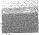
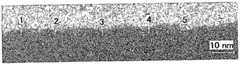
图26A和26B是氧化物半导体层的截面的TEM照片。26A and 26B are TEM photographs of a cross section of an oxide semiconductor layer.
图27A和27B是氧化物半导体层的截面的TEM照片。27A and 27B are TEM photographs of a cross section of an oxide semiconductor layer.
图28A和28B是氧化物半导体层的截面的TEM照片。28A and 28B are TEM photographs of a cross section of an oxide semiconductor layer.
图29A和29B分别是氧化物半导体层的截面的TEM照片和电子衍射图。29A and 29B are a TEM photograph and an electron diffraction diagram of a cross section of an oxide semiconductor layer, respectively.
图30是氧化物半导体层的EDX分析频谱。FIG. 30 is an EDX analysis spectrum of an oxide semiconductor layer.
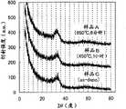
图31是氧化物半导体层的X光衍射图。Fig. 31 is an X-ray diffraction diagram of an oxide semiconductor layer.
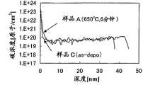
图32A到32C是氧化物半导体层的SIMS分析深度分布。32A to 32C are SIMS analysis depth profiles of an oxide semiconductor layer.
图33是简要说明科学计算的示意图。Fig. 33 is a schematic diagram briefly explaining scientific calculation.
图34A和34B是简要说明科学计算的示意图。34A and 34B are diagrams briefly explaining scientific calculations.
图35A和35B是说明科学计算机的示意图。35A and 35B are schematic diagrams illustrating a scientific computer.
图36是示出氧化物半导体的晶体结构的示意图。FIG. 36 is a schematic diagram showing a crystal structure of an oxide semiconductor.
图37A和37B示出了还没有经过-BT测试的和已经经过-BT测试的晶体管的I-V特性。37A and 37B show the I-V characteristics of transistors that have not undergone the -BT test and those that have undergone the -BT test.
图38A到38C是氧化物半导体层的SIMS分析深度分布。38A to 38C are SIMS analysis depth profiles of an oxide semiconductor layer.
图39A到39C是氧化物半导体层的SIMS分析深度分布。39A to 39C are SIMS analysis depth profiles of an oxide semiconductor layer.
具体实施方式Detailed ways
实施例和实例将参照附图来描述。注意,本发明并不限于下列描述,并且本领域技术人员应当容易理解,在不脱离本发明的精神和范围的情况下能够按照各种方式来修改本发明的模式和细节。因此,本发明不应被理解为仅限于以下关于实施例和实例的描述。注意,在以下所描述的本发明的结构中,相同的部分或者具有相似功能的部分在不同的附图中以相同的参考数字来表示,并且省略其描述。Embodiments and examples will be described with reference to the drawings. Note that the present invention is not limited to the following description, and it will be easily understood by those skilled in the art that the modes and details of the present invention can be modified in various ways without departing from the spirit and scope of the present invention. Therefore, the present invention should not be construed as being limited to the following description of the embodiments and examples. Note that in the structure of the present invention described below, the same parts or parts having similar functions are denoted by the same reference numerals in different drawings, and descriptions thereof are omitted.
(实施例1)(Example 1)
在本实施例中,晶体管的结构将参照图1A和1B来描述。In this embodiment, the structure of the transistor will be described with reference to FIGS. 1A and 1B.
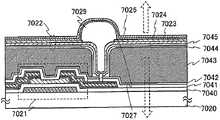
图1A是沟道蚀刻型晶体管的截面图,而图4A是其平面图。图1A是沿图4A的线A1-A2截取的截面图。FIG. 1A is a cross-sectional view of a channel-etched transistor, and FIG. 4A is a plan view thereof. FIG. 1A is a cross-sectional view taken along line A1 - A2 of FIG. 4A .
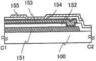
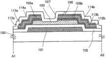
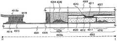
在图1A和1B中所示出的晶体管各自包括在基板100之上的栅极电极层101、栅极绝缘层102、包括在浅表部分内的结晶区106的氧化物半导体层103、源极电极层105a和漏极电极层105b。氧化物绝缘层107被设置于包括在浅表部分内的结晶区106的氧化物半导体层103、源极电极层105a和漏极电极层105b之上。The transistors shown in FIGS. 1A and 1B each include a
注意,图1A示出了正常沟道蚀刻型晶体管的结构,其中在源极电极层105a与漏极电极层105b之间的部分氧化物半导体层被蚀刻;但是,可以替代地采用其中氧化物半导体层没有被蚀刻从而如图1B所示出的那样留下在浅表部分内的结晶区的结构。Note that FIG. 1A shows the structure of a normal channel etching type transistor in which a part of the oxide semiconductor layer between the
栅极电极层101能够以使用诸如铝、铜、钼、钛、铬、钽、钨、钕及钪之类的任何金属材料,含有这些金属材料中的任何种作为其主要成分的合金材料或者含有这些金属材料中的任何种的氮化物的单层结构或层状结构来形成。在将诸如铝或铜之类的低电阻金属材料用于电极层的情况下,低电阻金属材料优选地结合难熔金属材料来使用,因为它具有诸如低耐热性和易于腐蚀之类的缺点。作为难熔金属材料,能够使用钼、钛、铬、钽、钨、钕、钪等。The
此外,为了提高像素部分的开口率,可以将氧化铟、氧化铟和氧化锡的合金、氧化铟和氧化锌的合金、氧化锌、氧化锌铝、氧氮化锌铝、氧化锌镓等透光氧化物导电层用作栅极电极层101。In addition, in order to increase the aperture ratio of the pixel part, indium oxide, an alloy of indium oxide and tin oxide, an alloy of indium oxide and zinc oxide, zinc oxide, zinc aluminum oxide, zinc aluminum oxynitride, zinc gallium oxide, etc. An oxide conductive layer is used as the
作为栅极绝缘层102,能够使用氧化硅、氧氮化硅、氮氧化硅、氮化硅、氧化铝、氧化钽等中的任何种的单层膜或层合膜。此类膜能够以CVD法、溅射法等来形成。As the
作为氧化物半导体膜,能够使用以InMO3(ZnO)m(m>0)表示的薄膜。在此,M代表选自Ga、Al、Mn和Co的一种或多种金属元素。例如,M可以是Ga、Ga和Al、Ga和Mn、Ga和Co等。在以InMO3(ZnO)m(m>0)表示的氧化物半导体膜当中,包含作为M的Ga的氧化物半导体被称为In-Ga-Zn-O基氧化物半导体,以及In-Ga-Zn-O基氧化物半导体的薄膜同样被称为In-Ga-Zn-O基膜。As the oxide semiconductor film, a thin film represented by InMO3 (ZnO)m (m>0) can be used. Here, M represents one or more metal elements selected from Ga, Al, Mn and Co. For example, M may be Ga, Ga and Al, Ga and Mn, Ga and Co, or the like. Among oxide semiconductor films represented by InMO3 (ZnO)m (m>0), an oxide semiconductor containing Ga as M is called an In-Ga-Zn-O-based oxide semiconductor, and In-Ga- A thin film of a Zn-O-based oxide semiconductor is also called an In-Ga-Zn-O-based film.
氧化物半导体层103以溅射法形成达10-300nm的厚度,优选地为20-100nm。应当注意,在氧化物半导体层103的一部分按照图1A所示的那样来蚀刻的情况下,当器件完成时,氧化物半导体层103具有其厚度小于以上厚度的区域。The
作为氧化物半导体层103,使用以RTA法等在高温下对其执行短时间的脱水或脱氢的那一种。脱水或脱氢能够通过以高温气体(惰性气体,例如,氮气或稀有气体)或光在500℃-750℃(或者低于或等于玻璃基板的应变点的温度)下的进行大约1分钟到10分钟,优选地为在650℃下进行大约3分钟到6分钟的快速热退火(RTA)处理来执行。以RTA法,能够短时间地执行脱水或脱氢;因此,该处理甚至能够在高于玻璃基板的应变点的温度下执行。As the
氧化物半导体层103是在形成氧化物半导体层103的阶段具有许多悬挂键的非结晶层。通过用于脱水或脱氢的加热步骤,短距离内的悬挂键彼此键合,使得氧化物半导体层103能够具有有序的非晶结构。随着排序进行,氧化物半导体层103变成为由非晶质和微晶的混合物形成,其中非晶区以微晶来点缀,或者由微晶群形成。在此,微晶是具有1-20nm的粒子尺寸的所谓纳米晶体,该粒子尺寸小于一般称为微晶的微晶粒子的粒子尺寸。The
在作为结晶区106的氧化物半导体层103的浅表部分内,优选地形成其中微晶是沿垂直于该层的表面的方向的c轴取向的微晶层。在这种情况下,晶体的长轴是沿着c轴方向的,而沿短轴方向的晶体管为1-20nm。In the superficial portion of the
在具有该结构的氧化物半导体层的浅表部分内,存在着包含微晶的致密的结晶区,并因而,能够防止由归因于湿气进入浅表部分或者氧自浅表部分排除的转变为n型所致的电特性降低。此外,由于氧化物半导体层的浅表部分位于背沟道侧,防止氧化物半导体层转变为n型对于抑制寄生沟道的生成同样是有效的。而且,能够降低在其处电导由于结晶区的存在而增加的浅表部分与源极电极层105a或漏极电极层105b之间的接触电阻。In the superficial part of the oxide semiconductor layer having this structure, there is a dense crystalline region containing microcrystals, and thus, it is possible to prevent the transition due to entry of moisture into the superficial part or exclusion of oxygen from the superficial part. It is a reduction in electrical characteristics due to the n-type. Furthermore, since the superficial portion of the oxide semiconductor layer is located on the back channel side, preventing the transition of the oxide semiconductor layer to n-type is also effective for suppressing the generation of parasitic channels. Also, it is possible to reduce the contact resistance between the superficial portion where the conductance increases due to the presence of the crystalline region and the
在此,可能生长的In-Ga-Zn-O基膜的晶体结构取决于用于沉积氧化物半导体的靶子。例如,在使用用于沉积氧化物半导体的靶子来形成In-Ga-Zn-O基膜,并且晶化通过加热步骤来执行的情况下,其中该In-Ga-Zn-O基膜含有In、Ga和Zn,使得In2O3对Ga2O3对ZnO之比为摩尔比1∶1∶1,则可能形成其中含有Ga和Zn的一个氧化物层或两个氧化物层混合于氧化铟层之间的六方晶系层状化合物晶体结构。作为选择,在使用其In2O3对Ga2O3对ZnO之比为摩尔比1∶1∶2的靶子,并且晶化通过加热步骤来执行的情况下,则插入氧化铟层之间的含有Ga和Zn的氧化物层可能具有双层结构。由于具有双层结构的后者的含有Ga和Zn的氧化物层的晶体结构是稳定的,并因而可能发生晶体生长,在使用其In2O3对Ga2O3对ZnO之比为摩尔比1∶1∶2的靶子,并且晶化通过加热步骤来执行的情况下,某些情况下会形成从含有Ga和Zn的氧化物层的外层到在栅极绝缘膜与含有Ga和Zn的氧化物层之间的界面连续的晶体。注意,摩尔比可以称为原子比。Here, the crystal structure of the In-Ga-Zn-O base film that may be grown depends on the target used to deposit the oxide semiconductor. For example, in the case where an In-Ga-Zn-O base film containing In, Ga and Zn, so that the ratio of In2 O3 to Ga2 O3 to ZnO is a molar ratio of 1:1:1, it is possible to form one oxide layer containing Ga and Zn or two oxide layers mixed with indium oxide Hexagonal layered compound crystal structure between layers. Alternatively, in case a target whose ratio of In2 O3 to Ga2 O3 to ZnO is molar ratio 1:1:2 is used, and the crystallization is performed by a heating step, then the An oxide layer containing Ga and Zn may have a double-layer structure. Since the crystal structure of the latter oxide layer containing Ga andZn having a double-layer structure is stable, and thus crystal growth may occur, when using its ratio ofIn2O3 toGa2O3 to ZnO as the molarratio 1:1:2 target, and crystallization is performed by a heating step, in some cases, a A continuous crystal at the interface between the oxide layers. Note that molar ratio may be referred to as atomic ratio.
注意,如图10A所示,在氧化物半导体层103的侧表面部分内没有形成结晶区,这取决于步骤的顺序,并且结晶区106仅形成于上层部分内。应当注意,侧表面部分的面积率低,并因而在这种情况下同样能够保持以上效果。Note that, as shown in FIG. 10A , no crystallization region is formed in the side surface portion of the
源极电极层105a具有第一导电层112a、第二导电层113a及第三导电层114a的三层结构,而漏极电极层105b具有第一导电层112b、第二导电层113b及第三导电层114b的三层结构。作为源极和漏极电极层105a和105b的材料,能够使用与栅极电极层101的材料类似的材料。The
此外,透光氧化物导电层按照与栅极电极层101的方式类似的方式用于源极和漏极电极层105a和105b,由此能够提高像素部分的透光率并且还能够提高开口率。In addition, a light-transmitting oxide conductive layer is used for the source and drain
此外,氧化物导电层可以形成于之间氧化物半导体层103与将要作为源极和漏极电极层105a和105b的上述金属膜之间,使得能够降低接触电阻。In addition, an oxide conductive layer may be formed between the
起着沟道保护层的作用的氧化物绝缘层107被设置于氧化物半导体层103、源极电极层105a和漏极电极层105b之上。氧化物绝缘层通过溅射法使用无机绝缘膜(典型地为氧化硅膜、氮氧化硅膜、氧化铝膜、氧氮化铝膜等)来形成。An
作为选择,在图10B中示出的底接触型晶体管可以通过将相似的材料用于每个部分而形成。Alternatively, a bottom-contact type transistor shown in FIG. 10B may be formed by using a similar material for each part.
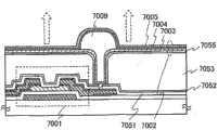
在图10B中示出的晶体管包括在基板100之上的栅极电极层101、栅极绝缘层102、源极电极层105a、漏极电极层105b以及包含在浅表部分内的结晶区106的氧化物半导体层103。此外,氧化物绝缘层107被设置于栅极绝缘层102、源极电极层105a、漏极电极层105b和氧化物半导体层103之上。The transistor shown in FIG. 10B includes a
同样地,在该结构中,氧化物半导体层103是非晶的或者由非晶质和微晶的混合物形成,其中除了包括结晶区106的浅表部分由微晶层形成之外,非晶区以微晶来点缀或者由微晶群形成。当使用具有该结构的氧化物半导体层时,能够按照与沟道蚀刻结构的方式相似的方式来防止由归因于湿气进入浅表部分或者氧自浅表部分排除的转变为n型所致的电特性降低。此外,由于氧化物半导体层的浅表部分位于背沟道侧并且包括由微晶层形成的结晶区,因而能够抑制寄生沟道的产生。Also, in this structure, the
具有该结构,晶体管能够具有高可靠性和高的电特性。With this structure, the transistor can have high reliability and high electrical characteristics.
注意,虽然在本实施例中给出了沟道蚀刻型晶体管的实例,但是可以使用沟道保护晶体管。作为选择,可以使用包括与源极电极层和漏极电极层重叠的氧化物半导体层的底接触型晶体管。Note that although an example of a channel etching type transistor is given in this embodiment, a channel protecting transistor may be used. Alternatively, a bottom-contact type transistor including an oxide semiconductor layer overlapping a source electrode layer and a drain electrode layer may be used.
注意,本实施例所描述的结构能够适当地结合其它实施例所描述的任何结构来使用。Note that the structure described in this embodiment can be used in combination with any structures described in other embodiments as appropriate.
(实施例2)(Example 2)
在本实施例中,包括实施例1所描述的沟道蚀刻型晶体管的显示设备的制造过程将参照图2A到2C、图3A到3C、图4A和4B、图5、图6、图7、图8A1、8A2、8B1和8B2及图9来描述。图2A到2C和图3A到3C是截面图,图4A和4B、图5、图6及图7是平面图,而在图4A和4B、图5、图6及图7中的线A1-A2和线B1-B2分别对应于在图2A到2C和图3A到3C的截面图中的线A1-A2和线B1-B2。In this embodiment, the manufacturing process of the display device including the channel-etched transistor described in
首先,制备基板100。作为基板100,能够使用下列基板中的任何种:以熔融法或浮法用钡硼硅酸盐玻璃、铝硼硅酸盐玻璃、铝硅酸盐玻璃等制成的非碱性玻璃基板,陶瓷基板,具有足以经受住该制造过程的处理温度的耐热性的塑料基板等。作为选择,可以使用金属基板,例如,具有设置有绝缘膜的表面的不锈钢合金基板。First, the
注意,代替以上所描述的玻璃基板,可以将使用绝缘体形成的基板(例如,陶瓷基板、石英基板或蓝宝石基板)用作基板100。Note that instead of the glass substrate described above, a substrate formed using an insulator (for example, a ceramic substrate, a quartz substrate, or a sapphire substrate) may be used as the
此外,作为基膜,绝缘膜还可以形成于基板100之上。基膜能够通过CVD法、溅射法等,使用氧化硅膜、氮化硅膜、氧氮化硅膜及氮氧化硅膜中的任何种的单层结构或层状结构来形成。在将含有可动离子的基板(例如,玻璃基板)用作基板100的情况下,含有氮的膜(例如,氮化硅膜或氮氧化硅膜)被用作基膜,由此能够防止可动离子进入半导体层。In addition, an insulating film may also be formed over the
然后,以溅射法或真空蒸发法将待成为包含栅极电极层101、电容器布线108及第一端子121的栅极布线的导电膜形成于基板100的整个表面之上。然后,通过第一光刻过程,形成抗蚀剂掩模。通过蚀刻来去除非必要部分,以形成布线和电极(栅极布线包括电极层101、电容器布线108及第一端子121)。此时,优选地执行蚀刻,使得栅极电极层101的末端部分成锥形,以便避免形成于栅极电极层101之上的膜破裂。图2A示出了本阶段的截面图。注意,图4B是本阶段的平面图。Then, a conductive film to be a gate wiring including the
包括栅极电极层101、电容器布线108以及在端子部分内的第一端子121的栅极布线能够以使用诸如铝、铜、钼、钛、铬、钽、钨、钕及钪之类的任何金属材料,含有这些金属材料中的任何种作为其主要成分的合金材料或者含有这些金属材料中的任何种的氮化物的单层结构或层状结构来形成。在将诸如铝或铜之类的低电阻金属材料用于电极层的情况下,低电阻金属材料优选地结合难熔金属材料来使用,因为它具有诸如低耐热性或易于腐蚀之类的缺点。作为难熔金属材料,能够使用钼、钛、铬、钽、钨、钕、钪等。The gate wiring including the
例如,作为栅极电极层101的双层结构,下列结构是优选的:其中钼层堆叠于铝层之上的双层结构、其中钼层堆叠于铜层之上的双层结构、其中氮化钛层或氮化钽层堆叠于铜层之上的双层结构以及氮化钛层和钼层的双层结构。作为三层结构,下列结构是优选的:包括在中间层的铝、铝和硅的合金、铝和钛的合金或者铝和钕的合金以及在顶层和底层的钨、氮化钨、氮化钛和钛中的任何种的层状结构。For example, as the double-layer structure of the
在那时,透光氧化物导电层被用于电极层和布线层的一部分以提高开口率。例如,能够将氧化铟、氧化铟和氧化锡的合金、氧化铟和氧化锌的合金、氧化锌、氧化锌铝、氧氮化锌铝、氧化锌镓等用于氧化物导电层。At that time, a light-transmitting oxide conductive layer was used for the electrode layer and a part of the wiring layer to increase the aperture ratio. For example, indium oxide, an alloy of indium oxide and tin oxide, an alloy of indium oxide and zinc oxide, zinc oxide, zinc aluminum oxide, zinc aluminum oxynitride, zinc gallium oxide, or the like can be used for the oxide conductive layer.
然后,在栅极电极层101之上形成栅极绝缘层102。栅极绝缘层102以CVD法、溅射法等形成达50-250nm的厚度。Then, a
例如,对于栅极绝缘层102,以溅射法来形成具有100nm的厚度的氧化硅膜。不必说,栅极绝缘层102并不限于此类氧化硅膜,而是可以以使用诸如氧氮化硅膜、氮氧化硅膜、氮化硅膜、氧化铝膜及氧化钽膜之类的任意绝缘膜的单层结构或层状结构来形成。For example, for the
作为选择,栅极绝缘层102可以通过CVD法与有机硅烷气体一起使用氧化硅层来形成。对于有机硅烷气体,能够使用含有硅的化合物,例如,正硅酸乙酯(TEOS)、四甲基硅烷(TMS)、四甲基环四硅氧烷(TMCTS)、八甲基环四硅氧烷(OMCTS)、六甲基二硅氮烷(HMDS)、三乙氧基硅烷(TRIES)或三(二甲胺基)硅烷(TDMAS)。Alternatively, the
作为选择,栅极绝缘层102可以使用铝、钇或铪的氧化物、氮化物、氧氮化物及氮氧化物,或者包含上述物质中的至少两种或更多种的化合物来形成。Alternatively, the
注意,在本说明书中,术语“氧氮化物”指的是含有氧原子和氮原子,使得氧原子数大于氮原子数的物质,术语“氮氧化物”指的是含有氮原子和氧原子,使得氮原子数大于氧原子数的物质。例如,“氧氮化硅膜”意指含有氧原子和氮原子,使得氧原子数大于氮原子数的,并且在使用卢瑟福背散射光谱法(RBS)和氢前向散射(HFS)来执行测量的情况下,含有浓度范围分别为50%-70%、0.5%-15%、25%-35%及0.1%-10%(原子百分比)的氧、氮、硅和氢的膜。此外,“氮氧化硅膜”意指含有氮原子和氧原子,使得氮原子数大于氧原子数的,并且在使用RBS和HFS来执行测量的情况下,含有浓度范围分别为5%-30%、20%-55%、25%-35%及10%-30%的氧、氮、硅和氢的膜。注意,氮、氧、硅和氢的百分比落在以上给出的范围之内,其中包含于氧氮化硅膜或氮氧化硅膜内的总原子数被定义为100%的原子百分比。Note that in this specification, the term "oxynitride" refers to a substance containing oxygen atoms and nitrogen atoms such that the number of oxygen atoms is greater than the number of nitrogen atoms, and the term "nitrogen oxide" refers to a substance containing nitrogen atoms and oxygen atoms, A substance that has more nitrogen atoms than oxygen atoms. For example, "silicon oxynitride film" means one containing oxygen atoms and nitrogen atoms such that the number of oxygen atoms is greater than the number of nitrogen atoms, and the In the case where the measurement was performed, films containing oxygen, nitrogen, silicon, and hydrogen in concentration ranges of 50%-70%, 0.5%-15%, 25%-35%, and 0.1%-10% (atomic percent), respectively. In addition, "silicon oxynitride film" means one containing nitrogen atoms and oxygen atoms such that the number of nitrogen atoms is greater than the number of oxygen atoms, and in the case of performing measurement using RBS and HFS, the containing concentration ranges from 5% to 30%, respectively , 20%-55%, 25%-35% and 10%-30% oxygen, nitrogen, silicon and hydrogen films. Note that the percentages of nitrogen, oxygen, silicon, and hydrogen fall within the ranges given above, in which the total number of atoms contained in the silicon oxynitride film or silicon oxynitride film is defined as an atomic percentage of 100%.
注意,在用于形成氧化物半导体层103的氧化物半导体膜形成之前,在栅极绝缘层的表面上的灰尘优选地通过执行其中引入氩气并生成等离子体的反向溅射来去除。反向溅射指的是其中使用RF电源来将电压施加于氩气气氛中的基板侧,从而在基板周围生成等离子体以使表面改性的方法。注意,代替氩气气氛,可以使用氮气气氛、氦气气氛等。作为选择,可以使用其中添加了氧气、N2O等的氩气气氛。同样作为选择,可以使用其中添加了Cl2、CF4等的氩气气氛。在反向溅射之后,氧化物半导体膜在不暴露于空气的情况下形成,由此能够防止灰尘和湿气附着于栅极绝缘层102与氧化物半导体层103之间的界面上。Note that before the formation of the oxide semiconductor film for forming the
然后,氧化物半导体膜被形成于栅极绝缘层102之上,达5-200nm的厚度,优选地为10-40nm。Then, an oxide semiconductor film is formed over the
作为氧化物半导体膜,能够使用四组分金属氧化物膜,例如,In-Sn-Ga-Zn-O基膜;三组分金属氧化物膜,例如,In-Ga-Zn-O基膜、In-Sn-Zn-O基膜、In-Al-Zn-O基膜、Sn-Ga-Zn-O基膜、Al-Ga-Zn-O基膜或Sn-Al-Zn-O基膜;或者二组分金属氧化物膜,例如,In-Zn-O基膜、Sn-Zn-O基膜、Al-Zn-O基膜、Zn-Mg-O基膜、Sn-Mg-O基膜或In-Mg-O基膜;In-O基膜、Sn-O基膜或Zn-O基膜。此外,氧化物半导体膜还可以含有SiO2。As the oxide semiconductor film, a four-component metal oxide film, for example, an In-Sn-Ga-Zn-O base film; a three-component metal oxide film, for example, an In-Ga-Zn-O base film, In-Sn-Zn-O base film, In-Al-Zn-O base film, Sn-Ga-Zn-O base film, Al-Ga-Zn-O base film or Sn-Al-Zn-O base film; Or two-component metal oxide film, for example, In-Zn-O base film, Sn-Zn-O base film, Al-Zn-O base film, Zn-Mg-O base film, Sn-Mg-O base film Or In-Mg-O base film; In-O base film, Sn-O base film or Zn-O base film. In addition, the oxide semiconductor film may contain SiO2 .
在此,使用用于沉积氧化物半导体的靶子来形成氧化物半导体膜,该靶子含有In、Ga和Zn(In2O3对Ga2O3对ZnO之比为摩尔比1∶1∶1或1∶1∶2),在以下条件下:基板与靶子之间的距离为100mm,压力为0.6Pa,以及直流电(DC)功率为0.5kW,并且气氛为氧气气氛(氧气流量的比例为100%)。注意,当使用脉冲直流电(DC)电源时,能够减少灰尘并且膜厚度可能是均匀的。在本实施例中,作为氧化物半导体膜,30nm厚的In-Ga-Zn-O基膜以溅射法使用用于沉积In-Ga-Zn-O基氧化物半导体的靶子来形成。Here, the oxide semiconductor film is formed using a target for depositing an oxide semiconductor containing In, Ga, and Zn (the ratio of In2 O3 to Ga2 O3 to ZnO is a molar ratio of 1:1:1 or 1:1:2), under the following conditions: the distance between the substrate and the target is 100mm, the pressure is 0.6Pa, and the direct current (DC) power is 0.5kW, and the atmosphere is an oxygen atmosphere (the ratio of oxygen flow rate is 100% ). Note that when a pulsed direct current (DC) power source is used, dust can be reduced and the film thickness can be uniform. In this embodiment, as the oxide semiconductor film, a 30 nm-thick In-Ga-Zn-O-based film was formed by a sputtering method using a target for depositing an In-Ga-Zn-O-based oxide semiconductor.
溅射法的实例包括其中将高频电源用作溅射电源的RF溅射法、其中使用DC电源的DC溅射法以及其中按照脉冲的方式来施加偏压的脉冲DC溅射法。RF溅射法主要在形成绝缘膜的情况下使用,而DC溅射法主要在形成诸如金属膜之类的导电膜的情况下使用。Examples of the sputtering method include an RF sputtering method in which a high-frequency power source is used as a sputtering power source, a DC sputtering method in which a DC power source is used, and a pulsed DC sputtering method in which a bias voltage is applied in a pulsed manner. The RF sputtering method is mainly used in the case of forming an insulating film, and the DC sputtering method is mainly used in the case of forming a conductive film such as a metal film.
另外,还有其中能够设置多个不同材料的靶子的多源极溅射装置。以多源极溅射装置,不同材料的膜能够被形成以在同一腔室内堆叠,或者能够在同一腔室内同时形成多种材料的膜。In addition, there is also a multi-source sputtering apparatus in which a plurality of targets of different materials can be set. With a multi-source sputtering apparatus, films of different materials can be formed to be stacked in the same chamber, or films of multiple materials can be formed simultaneously in the same chamber.
另外,还有在腔室内设置有磁体系统,用于磁控溅射法的溅射装置,以及用于ECR溅射法的溅射装置,在ECR溅射法中,在不使用辉光放电的情况下使用利用微波产生的等离子体。In addition, there is a magnet system installed in the chamber, a sputtering device for the magnetron sputtering method, and a sputtering device for the ECR sputtering method. In the ECR sputtering method, without using glow discharge In this case, plasma generated using microwaves is used.
而且,作为使用溅射法的沉积方法,还有其中靶子物质与溅射气体成分在沉积期间相互化学反应以形成其化合物薄膜的反应溅射法,以及其中在沉积期间同样对基板施加电压的偏压溅射法。Also, as a deposition method using the sputtering method, there are reactive sputtering methods in which a target substance and sputtering gas components chemically react with each other during deposition to form a compound film thereof, and biasing methods in which a voltage is also applied to a substrate during deposition. pressure sputtering method.
然后,通过第二光刻过程,形成抗蚀剂掩模。然后,蚀刻In-Ga-Zn-O基膜。在蚀刻中,能够将诸如柠檬酸或草酸之类的有机酸用作蚀刻剂。在此,In-Ga-Zn-O基膜使用ITO-07N(Kanto化学股份有限公司制造)通过湿法蚀刻来蚀刻以去除非必要部分。因而,In-Ga-Zn-O基膜被处理以具有岛屿形状,由此形成氧化物半导体层103。氧化物半导体层103的末端部分被蚀刻为具有锥形形状,由此能够防止布线因阶梯形状所致的破裂。注意,蚀刻在此并不限于湿法蚀刻,而是可以执行干法蚀刻。Then, through a second photolithography process, a resist mask is formed. Then, the In-Ga-Zn-O base film is etched. In etching, an organic acid such as citric acid or oxalic acid can be used as an etchant. Here, the In-Ga-Zn-O base film was etched by wet etching using ITO-07N (manufactured by Kanto Chemical Co., Ltd.) to remove unnecessary parts. Thus, the In-Ga-Zn-O base film is processed to have an island shape, whereby the
然后,氧化物半导体层受到脱水或脱氢。用于脱水或脱氢的第一热处理能够通过使用高温气体(惰性气体,例如,氮气或稀有气体)或光在500℃-750℃的温度(或者低于或等于玻璃基板的应变点的温度)下进行大约1分钟到10分钟,优选地在650℃下进行大约3分钟到6分钟的快速热退火(RTA)处理来执行。以RTA法,能够短时间地执行脱水或脱氢;因此,该处理甚至能够在高于玻璃基板的应变点的温度下执行。本阶段的截面图以及本阶段的平面图分别示出于图2B和图5中。注意,热处理的时序并不限于该时序,而是可以多次执行,例如,在光刻过程或沉积步骤之前和之后。Then, the oxide semiconductor layer is dehydrated or dehydrogenated. The first heat treatment for dehydration or dehydrogenation can be performed at a temperature of 500°C to 750°C (or a temperature lower than or equal to the strain point of the glass substrate) by using a high-temperature gas (inert gas, for example, nitrogen or a rare gas) or light The rapid thermal annealing (RTA) treatment is performed at 650° C. for about 1 minute to 10 minutes, preferably at 650° C. for about 3 minutes to 6 minutes. With the RTA method, dehydration or dehydrogenation can be performed for a short time; therefore, the treatment can be performed even at a temperature higher than the strain point of the glass substrate. A cross-sectional view at this stage and a plan view at this stage are shown in Fig. 2B and Fig. 5, respectively. Note that the timing of heat treatment is not limited to this timing, but may be performed multiple times, for example, before and after a photolithography process or a deposition step.
在此,氧化物半导体层103的浅表部分通过第一热处理来晶化,并从而变成具有包含微晶的结晶区106。氧化物半导体层103的剩余部分变成为非结晶的或者由非晶质和微晶的混合物形成,其中非晶区以微晶来点缀或者由微晶群形成。注意,结晶区106是氧化物半导体层103的一部分,并且在下文中,“氧化物半导体层103”包括结晶区106。Here, the superficial portion of the
注意,在本说明书中,在惰性气体(例如,氮气或稀有气体)的气氛中的热处理被称为用于脱水或脱氢的热处理。在本说明书中,“脱氢”并非是指以热处理来仅排除H2。为了方便起见,H、OH等的排除也称为“脱水或脱氢”。Note that, in this specification, heat treatment in an atmosphere of an inert gas (for example, nitrogen or a rare gas) is referred to as heat treatment for dehydration or dehydrogenation. In the present specification, "dehydrogenation" does not mean only removing H2 by heat treatment. For convenience, the removal of H, OH, etc. is also referred to as "dehydration or dehydrogenation".
重要的是,受到过脱水或脱氢的氧化物半导体层不应当暴露于空气,从而能够防止水或氢进入氧化物半导体层之内。当晶体管使用通过执行脱水或脱氢将氧化物半导体层改变成低电阻氧化物半导体层(即,n型(例如,n-型或n+型)氧化物半导体层),以及通过将低电阻氧化物半导体层改变成高电阻氧化物半导体层使得氧化物半导体层变成i型氧化物半导体层而获得的氧化物半导体层来形成时,晶体管的阈值电压(Vth)是正的,从而实现所谓的常关性质。对于用于显示设备的晶体管而言,优选的是栅极电压是尽可能接近于0V的正的阈值电压。在有源矩阵显示设备中,包含于电路内的晶体管的电特性是重要的,并且显示设备的性能取决于电特性。特别地,晶体管的阈值电压是重要的。如果晶体管的阈值电压是负的,则晶体管具有所谓的常开性质,也就是,即使在栅极电压为0V时也有电流在源极电极与漏极电极之间流过,使得难以控制使用该晶体管形成的电路。在阈值电压为正,但阈值电压的绝对值为大的晶体管的情形中,该晶体管在某些情况下无法执行开关操作,因为驱动电压不是足够高的。在n沟道晶体管的情形中,优选的是在正电压被施加为栅极电压之后才形成沟道并且有漏极电流流过。其中除非驱动电压升高否则不形成沟道的晶体管以及其中即使在施加负电压时也会形成并且有漏极电流流过的晶体管不适用于在电路中使用的晶体管。It is important that the dehydrated or dehydrogenated oxide semiconductor layer should not be exposed to the air so that water or hydrogen can be prevented from entering into the oxide semiconductor layer. When the transistor is used, the oxide semiconductor layer is changed into a low-resistance oxide semiconductor layer (that is, an n-type (for example, n- type or n+ -type) oxide semiconductor layer) by performing dehydration or dehydrogenation, and by oxidizing the low-resistance When an oxide semiconductor layer obtained by changing the material semiconductor layer into a high-resistance oxide semiconductor layer so that the oxide semiconductor layer becomes an i-type oxide semiconductor layer is formed, the threshold voltage (Vth ) of the transistor is positive, thereby realizing the so-called Normally closed nature. For transistors used in display devices it is preferred that the gate voltage is a positive threshold voltage as close to 0V as possible. In an active matrix display device, the electrical characteristics of transistors included in a circuit are important, and the performance of the display device depends on the electrical characteristics. In particular, the threshold voltage of transistors is important. If the threshold voltage of the transistor is negative, the transistor has a so-called normally-on property, that is, a current flows between the source electrode and the drain electrode even when the gate voltage is 0V, making it difficult to control the use of the transistor formed circuit. In the case of a transistor whose threshold voltage is positive but the absolute value of the threshold voltage is large, the transistor cannot perform switching operation in some cases because the driving voltage is not sufficiently high. In the case of an n-channel transistor, it is preferable that a channel is formed and a drain current flow after a positive voltage is applied as a gate voltage. A transistor in which a channel is not formed unless a driving voltage is raised and a transistor in which a drain current flows even when a negative voltage is applied are not suitable for a transistor used in a circuit.
在从在其下执行脱水或脱氢的温度起的冷却中,气氛可以切换为与在其中升高温度或者执行热处理的气氛不同的气氛。例如,冷却能够在当炉子充满高纯度氧气、高纯度N2O气或超干燥空气(具有-40℃或更低的,优选地为-60℃或更低的露点)时于其中执行脱水或脱氢的炉子内执行,不暴露于空气。In cooling from the temperature at which dehydration or dehydrogenation is performed, the atmosphere may be switched to an atmosphere different from the atmosphere in which the temperature is raised or heat treatment is performed. For example, cooling can performdehydration or Dehydrogenation is performed in a furnace, not exposed to air.
注意,在第一热处理中,优选的是在气氛中不含有水、氢等。作为选择,被引入热处理装置之内的惰性气体的纯度优选地为6N(99.9999%)或更高,更优选地为7N(99.99999%)或更高(也就是,杂质浓度为1ppm或更低,优选地0.1ppm或更低)。Note that in the first heat treatment, it is preferable not to contain water, hydrogen, or the like in the atmosphere. Alternatively, the purity of the inert gas introduced into the heat treatment device is preferably 6N (99.9999%) or higher, more preferably 7N (99.99999%) or higher (that is, the impurity concentration is 1 ppm or lower, preferably 0.1 ppm or less).
在热处理于惰性气体气氛中执行的情况下,氧化物半导体层被改变成缺氧型氧化物半导体层,从而通过热处理使氧化物半导体层变成低电阻氧化物半导体层(即,n型(例如,n-型或n+型)氧化物半导体层)。其后,通过形成与氧化物半导体层接触的氧化物绝缘层而使氧化物半导体层变成为氧过量状态。因而,使氧化物半导体层成为i型的;也就是,氧化物半导体层被改变为高电阻氧化物半导体层。因此,有可能形成具有有利的电特性的高可靠性晶体管。In the case where the heat treatment is performed in an inert gas atmosphere, the oxide semiconductor layer is changed into an oxygen-deficient type oxide semiconductor layer, so that the oxide semiconductor layer becomes a low-resistance oxide semiconductor layer (that is, an n-type (eg, , n- type or n+ -type) oxide semiconductor layer). Thereafter, the oxide semiconductor layer is brought into an oxygen-excess state by forming an oxide insulating layer in contact with the oxide semiconductor layer. Thus, the oxide semiconductor layer is made i-type; that is, the oxide semiconductor layer is changed into a high-resistance oxide semiconductor layer. Therefore, it is possible to form a highly reliable transistor with favorable electrical characteristics.
氧化物半导体层可以部分晶化,取决于第一热处理的条件或者氧化物半导体层的材料。在第一热处理之后,获得了氧空缺且具有低电阻的氧化物半导体层103。在第一热处理之后,载流子浓度高于刚在膜形成之后的氧化物半导体膜的载流子浓度,使得氧化物半导体层具有优选地为1×10¹⁸/cm3或更高的载流子浓度。The oxide semiconductor layer may be partially crystallized depending on the conditions of the first heat treatment or the material of the oxide semiconductor layer. After the first heat treatment, the
用于氧化物半导体层的第一热处理可以在氧化物半导体膜被处理成岛状氧化物半导体层之前执行。在这种情况下,第二光刻过程在第一热处理之后执行。结晶区没有形成于岛状氧化物半导体层103的侧表面部分内,而是结晶区106仅形成于氧化物半导体层103的上层部分内(参见图10A)。The first heat treatment for the oxide semiconductor layer may be performed before the oxide semiconductor film is processed into the island-shaped oxide semiconductor layer. In this case, the second photolithography process is performed after the first heat treatment. The crystalline region is not formed in the side surface portion of the island-shaped
然后,通过第三光刻过程,形成抗蚀剂掩模。非必要部分通过蚀刻来去除以形成达到由与栅极电极层101相同的材料形成的布线或电极层的接触孔。该接触孔被提供用于连接上述布线等与后面将要形成的导电膜。Then, through a third photolithography process, a resist mask is formed. Unnecessary portions are removed by etching to form contact holes reaching wiring or electrode layers formed of the same material as the
然后,在氧化物半导体层103和栅极绝缘层102之上,以溅射法或真空蒸发法形成作为导电层的第一导电层112、第二导电层113和第三导电层114。图2C是本阶段的截面图。Then, over the
第一导电层112、第二导电层113和第三导电层114能够各自使用与栅极电极层101的材料相似的材料来形成。The first
在此,第一导电层112和第三导电层114使用为耐热性导电材料的钛来形成,而第二导电层113使用含有钕的铝合金形成。该结构能够利用铝的低电阻性质并且减少凸起产生。注意,虽然导电层在本实施例中具有三层结构,但是本发明的实施例并不限于此。可以采用单层结构或者包括两层或四层或者更多层的层状结构。例如,可以采用钛膜的单层结构或者钛膜和含有硅的铝膜的层状结构。Here, the first
然后,通过第四光刻过程,形成抗蚀剂掩模131。非必要部分通过蚀刻来去除,由此形成源极和漏极电极层105a和105b、氧化物半导体层103以及连接电极120。此时采用湿法蚀刻或干法蚀刻来作为蚀刻方法。例如,当第一导电层112和第三导电层114使用钛形成以及第二导电层113使用含有钕的铝合金形成时,湿法蚀刻能够通过将溶液或加热的盐酸用作蚀刻剂来执行。通过该蚀刻步骤,氧化物半导体层103被部分蚀刻以具有在源极电极层105a与漏极电极层105b之间的薄的区域。本阶段的截面图和本阶段的平面图分别示出于图3A和图6中。Then, through a fourth photolithography process, a resist
此时,蚀刻处理在氧化物半导体层103对第一导电层112和第三导电层114的选择比为足够低的条件下执行,由此晶体管具有如图1B所示出的那样留下了浅表部分的结晶区的结构。At this time, the etching process is performed under the condition that the selectivity ratio of the
第一导电层112、第二导电层113、第三导电层114及氧化物半导体层103能够使用过氧化氢溶液或加热的盐酸来完全蚀刻。因此,在源极电极层105a、漏极电极层105b或氧化物半导体层103的末端部分没有形成阶梯等。另外,湿法蚀刻允许各层各向同性地蚀刻;因而,源极和漏极电极层105a和105b被减小尺寸,使得它们的末端部分位于抗蚀剂掩模131的内侧。通过以上步骤,能够制造出其中氧化物半导体层103和结晶区106被用作沟道形成区的晶体管170。The first
在此,源极电极层105a和漏极电极层105b使用与栅极电极层101类似的透光氧化物导电层来形成,由此能够提高像素部分的透光率并且还能够提高开口率。Here, the
此外,氧化物导电层可以形成于氧化物半导体层103与将要成为源极和漏极电极层105a和105b的金属膜之间,从而能够降低接触电阻。In addition, an oxide conductive layer can be formed between the
在第四光刻过程中,使用与源极电极层105a和漏极电极层105b相同的材料形成的第二端子122也留在了端子部分内。注意,第二端子122与源极布线(包括源极和漏极电极层105a和105b的源极布线)电连接。In the fourth photolithography process, the
另外,在端子部分内,连接电极120通过形成于栅极绝缘层102内的接触孔直接连接到端子部分的第一端子121。注意,虽然没有示出,但是驱动电路的晶体管的源极或漏极布线及栅极电极通过与以上步骤相同的步骤彼此直接连接。In addition, in the terminal portion, the
此外,通过使用具有多个厚度(典型为两个不同的厚度)的区域的,使用多色调掩模形成的抗蚀剂掩模,能够减少抗蚀剂掩模的数量,从而造成简化的过程和较低的成本。Furthermore, by using a resist mask formed using a multi-tone mask with regions having multiple thicknesses (typically two different thicknesses), the number of resist masks can be reduced, resulting in simplified processes and lower cost.
然后,去除抗蚀剂掩模131,并且形成覆盖晶体管170的氧化物绝缘层107。氧化物绝缘层107能够使用氧化硅膜、氧氮化硅膜、氧化铝膜、氧化钽膜等来形成。Then, the resist
在本实施例中,以溅射法将氧化硅膜形成用于氧化物绝缘层。在膜形成中的基板温度可以是从室温到300℃,而在本实施例中,是100℃。为了在膜形成中防止诸如水或氢之类的杂质进入,优选的是在膜形成之前,在降低的压力之下于150℃-350℃的温度下执行2-10分钟的预烘焙,以在不暴露于空气的情况下形成氧化物绝缘层。氧化硅膜能够以溅射法在稀有气体(典型为氩气)气氛、氧气气氛或者含有稀有气体(典型为氩气)和氧气的混合气氛中形成。此外,还能够将氧化硅靶或硅靶用作靶子。例如,使用硅靶,氧化硅膜能够以溅射法在氧气和稀有气体的气氛中形成。被形成为与在其电阻被降低的区域内的氧化物半导体层接触的氧化物绝缘层使用不含有诸如湿气、氢离子和OH-之类的杂质并且阻挡此类杂质从外部进入的无机绝缘膜来形成。In this embodiment, a silicon oxide film is formed for the oxide insulating layer by a sputtering method. The substrate temperature in film formation can be from room temperature to 300°C, and in this embodiment, it is 100°C. In order to prevent entry of impurities such as water or hydrogen during film formation, it is preferable to perform prebaking at a temperature of 150° C. to 350° C. for 2 to 10 minutes under reduced pressure before film formation to The oxide insulating layer is formed without exposure to air. The silicon oxide film can be formed by sputtering in a rare gas (typically argon) atmosphere, an oxygen atmosphere, or a mixed atmosphere containing a rare gas (typically argon) and oxygen. In addition, a silicon oxide target or a silicon target can also be used as the target. For example, using a silicon target, a silicon oxide film can be formed in an atmosphere of oxygen and a rare gas by a sputtering method. The oxide insulating layer formed to be in contact with the oxide semiconductor layer in a region whose resistance is lowered uses an inorganic insulating layer that does not contain impurities such as moisture, hydrogen ions, and OH− and blocks entry of such impurities from the outside. film to form.
在本实施例中,膜形成通过脉冲DC溅射法使用以柱状多晶B(具有0.01Ω·cm的电阻率)掺杂的硅靶在以下条件执行并且具有6N纯度:在基板与靶子之间的距离(T-S距离)为89mm,压力为0.4Pa,以及直流电(DC)功率为6kW,并且气氛是氧气气氛(氧气流量的比例为100%)。厚度为300nm。In this example, film formation was performed by a pulsed DC sputtering method using a silicon target doped with columnar polycrystalline B (with a resistivity of 0.01 Ω·cm) under the following conditions and with a purity of 6N: Between the substrate and the target The distance (T-S distance) is 89 mm, the pressure is 0.4 Pa, and the direct current (DC) power is 6 kW, and the atmosphere is an oxygen atmosphere (the ratio of oxygen flow rate is 100%). The thickness is 300nm.
然后,在惰性气体气氛中执行第二热处理(优选地,在200℃-400℃的温度下,例如,250℃-350℃)。例如,第二热处理在氮气气氛中于250℃下执行1小时。作为选择,如同在第一热处理中那样,RTA处理可以在高温下短时间地执行。在第二热处理中,由于氧化物绝缘层107被加热成与氧化物半导体层103的一部分接触,因而氧由氧化物绝缘层107供应给变成为n型的并且通过第一热处理而具有较低电阻的氧化物半导体层103,使得氧化物半导体层103处于氧过量状态。因而,氧化物半导体层103能够是i型的(具有较高的电阻)。Then, a second heat treatment is performed in an inert gas atmosphere (preferably, at a temperature of 200° C. to 400° C., for example, 250° C. to 350° C.). For example, the second heat treatment is performed at 250° C. for 1 hour in a nitrogen atmosphere. Alternatively, as in the first heat treatment, RTA treatment may be performed at a high temperature for a short time. In the second heat treatment, since the
在本实施例中,第二热处理在氧化硅膜形成之后执行;但是,热处理的时序并不限于刚形成氧化硅膜之后的时序,只要是在氧化硅膜形成之后即可。In this embodiment, the second heat treatment is performed after the formation of the silicon oxide film; however, the timing of the heat treatment is not limited to the timing immediately after the formation of the silicon oxide film as long as it is after the formation of the silicon oxide film.
在源极电极层105a和漏极电极层105b使用耐热材料形成的情况下,使用第一热处理的条件的步骤能够在第二热处理的时序执行。在这种情况下,热处理可以在氧化硅膜形成之后就立即执行。In the case where the
然后,通过执行第五光刻过程,形成抗蚀剂掩模。氧化物绝缘层107被蚀刻,从而形成达到漏极电极层105b的接触孔125。另外,达到连接电极120的接触孔126以及达到第二端子122的接触孔127同样通过该蚀刻来形成。图3B是本阶段的截面图。Then, by performing a fifth photolithography process, a resist mask is formed. The
然后,在去除了抗蚀剂掩模之后形成透光导电膜。通过溅射法、真空蒸发法等使用氧化铟(In2O3)、氧化铟和氧化锡的合金(In2O3-SnO2,以下缩写为ITO)等来形成透光导电膜。该材料以盐酸基溶液来蚀刻。应当注意,由于在蚀刻ITO时可能产生残留物,因而可以使用氧化铟和氧化锌的合金(In2O3-ZnO,以下缩写为IZO)来提高蚀刻加工性能。Then, a light-transmitting conductive film is formed after the resist mask is removed. The light-transmitting conductive film is formed using indium oxide (In2 O3 ), an alloy of indium oxide and tin oxide (In2 O3 -SnO2 , hereinafter abbreviated as ITO), or the like by a sputtering method, a vacuum evaporation method, or the like. The material is etched with a hydrochloric acid based solution. It should be noted that an alloy of indium oxide and zinc oxide (In2 O3 —ZnO, hereinafter abbreviated as IZO) may be used to improve etching processability since residues may be generated when etching ITO.
然后,通过第六光刻过程,形成抗蚀剂掩模。透光导电膜的非必要部分通过蚀刻来去除,从而形成像素电极层110。在此,储能电容器以在电容器部分内用作电介质的栅极绝缘层102和氧化物绝缘层107、电容器布线108和像素电极层110来形成。Then, through a sixth photolithography process, a resist mask is formed. Unnecessary portions of the light-transmitting conductive film are removed by etching, thereby forming the
此外,在第六光刻过程和蚀刻步骤中,透光导电层128和129分别形成于第一端子121和第二端子122之上。透光导电层128和129各自用作电极或者与FPC连接的布线。与第一端子121连接的透光导电层128是起着栅极布线的输入端子的作用的连接端子电极。形成于第二端子122之上的透光导电层129用作起着源极布线的输入端子的作用的连接端子电极。In addition, in the sixth photolithography process and etching step, light-transmitting
然后,去除抗蚀剂掩模。本阶段的截面图和本阶段的平面图分别示出于图3C和图7中。Then, the resist mask is removed. A cross-sectional view at this stage and a plan view at this stage are shown in Figures 3C and 7, respectively.
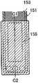
图8A1和8A2分别是本阶段的栅极布线端子部分的截面图及其平面图。图8A1是沿图8A2的线C1-C2截取的截面图。在图8A1中,透光导电层155形成于保护绝缘膜154之上,并且连接电极153是起着输入端子的作用的连接端子电极。此外,在图8A1中,由与栅极布线相同的材料形成的第一端子151以及由与源极布线相同的材料形成的连接电极153彼此重叠(栅极绝缘层152插入它们之间),并且彼此部分直接接触以及电连接。而且,连接电极153和透光导电层155通过形成于保护绝缘膜154内的接触孔彼此直接连接。8A1 and 8A2 are a cross-sectional view of a gate wiring terminal portion at this stage and a plan view thereof, respectively. FIG. 8A1 is a cross-sectional view taken along line C1 - C2 of FIG. 8A2 . In FIG. 8A1 , a light-transmitting
图8B1和8B2分别是源极布线端子部分的截面图及其平面图。图8B1是沿图8B2的线D1-D2截取的截面图。在图8B1中,形成于保护绝缘膜154和连接电极150之上的透光导电层155是起着输入端子的作用的连接端子电极。此外,在图8B1中,由与栅极布线相同的材料形成的第二端子156与电连接至源极布线的连接电极150重叠,栅极绝缘层152插入它们之间。第二端子156没有与连接电极150电连接,并且当第二端子156的电位被设置为与连接电极150的电位不同的电位,例如,GND或0V,或者第二端子156被设置为浮置状态时,能够形成用于防止噪声或静电的电容器。连接电极150通过形成于保护绝缘膜154内的接触孔与透光导电层155电连接。8B1 and 8B2 are a sectional view of a source wiring terminal portion and a plan view thereof, respectively. FIG. 8B1 is a cross-sectional view taken along line D1-D2 of FIG. 8B2. In FIG. 8B1 , the light-transmitting
根据像素密度来提供多条栅极布线、源极布线及电容器布线。同样,在端子部分中,排布了电位与栅极布线相同的多个第一端子、电位与源极布线相同的多个第二端子、电位与电容器布线相同的多个第三端子等。每种端子的数量可以是任何数量,并且端子的数量可以由实施人酌情而定。A plurality of gate wirings, source wirings, and capacitor wirings are provided according to pixel density. Also, in the terminal portion, a plurality of first terminals having the same potential as the gate wiring, a plurality of second terminals having the same potential as the source wiring, a plurality of third terminals having the same potential as the capacitor wiring, and the like are arranged. The number of each type of terminal can be any number, and the number of terminals can be determined by the implementer as appropriate.
通过这六个光刻过程,从而能够完成沟道蚀刻型晶体管170和储能电容器部分。通过将晶体管和储能电容器布置于像素部分内的矩阵中,能够获得用于制造有源矩阵显示设备的基板之一。在本说明书中,为方便起见,将此类基板称为有源矩阵基板。Through these six photolithography processes, the channel
在制造有源矩阵液晶显示设备的情况下,有源矩阵基板与设置有对电极的对基板彼此接合,液晶层插入它们之间。注意,与在对基板上的对电极电连接的公共电极被设置于有源矩阵基板之上,以及与公共电极电连接的第四端子被设置于端子部分内。提供第四端子使得公共电极被设置为固定电位,例如,GND或0V。In the case of manufacturing an active matrix liquid crystal display device, an active matrix substrate and a counter substrate provided with a counter electrode are bonded to each other with a liquid crystal layer interposed therebetween. Note that a common electrode electrically connected to the counter electrode on the counter substrate is provided on the active matrix substrate, and a fourth terminal electrically connected to the common electrode is provided in the terminal portion. The fourth terminal is provided so that the common electrode is set to a fixed potential, for example, GND or 0V.
本实施例的像素结构并不限于图7内的像素结构。图9是示出另一种像素结构的实例的平面图。图9示出了其中不提供电容器布线并且储能电容器以彼此重叠的像素电极和相邻像素的栅极布线(保护绝缘膜和栅极绝缘层插入它们之间)来形成的实例。在这种情况下,能够省略电容器布线以及与电容器布线连接的第三端子。注意,在图9中,与图7中的部分相同的部分以共同的参考数字来表示。The pixel structure of this embodiment is not limited to the pixel structure in FIG. 7 . Fig. 9 is a plan view showing another example of a pixel structure. 9 shows an example in which no capacitor wiring is provided and a storage capacitor is formed with pixel electrodes and gate wirings of adjacent pixels overlapping each other with a protective insulating film and a gate insulating layer interposed therebetween. In this case, the capacitor wiring and the third terminal connected to the capacitor wiring can be omitted. Note that in FIG. 9, the same parts as those in FIG. 7 are denoted by common reference numerals.
在有源矩阵液晶显示设备中,显示图形通过驱动按阵列排布的液晶元件来形成。具体地,通过将电压施加于包含于所选的液晶元件内的像素电极与对电极之间,执行液晶层的光学调制,并且该光学调制由观看者感知为显示图形。In an active matrix liquid crystal display device, display patterns are formed by driving liquid crystal elements arranged in an array. Specifically, by applying a voltage between a pixel electrode included in a selected liquid crystal element and a counter electrode, optical modulation of the liquid crystal layer is performed, and the optical modulation is perceived by a viewer as a display pattern.
在显示液晶显示设备的运动图像时,存在着液晶分子本身的长响应时间导致余像的问题。为了减少此类余像,采用了一种称为黑插(blackinsertion)的驱动方法,在该驱动方法中,每隔一个帧周期就在整个屏幕上显示黑色。When displaying moving images of a liquid crystal display device, there is a problem that the long response time of the liquid crystal molecules themselves causes afterimages. In order to reduce such afterimages, a driving method called black insertion (black insertion) is employed in which black is displayed on the entire screen every other frame period.
此外,还有另一种称为双倍帧率驱动的驱动技术。在双倍帧率驱动中,垂直同步频率被设置为高至普通垂直同步频率的1.5倍或更高,优选为2倍或更高,由此提高响应速度,并且在每一帧内为已经通过划分而获得的每多个场选择待写入的灰度。In addition, there is another driving technology called double frame rate driving. In double frame rate driving, the vertical sync frequency is set to be as high as 1.5 times or more, preferably 2 times or more, the normal vertical sync frequency, thereby improving the response speed, and the A gray scale to be written is selected for every plurality of fields obtained by division.
而且,存在一种驱动技术,用以通过将多个LED(发光二极管)、多个EL光源等用作背光而形成平面光源,并且平面光源的每个光源被单独使用以在一个帧周期内执行间歇性照明驱动。例如,在使用LED的情况下,并非总是使用白色的LED,而是可以使用三种或更多颜色的LED。由于能够单独控制多个LED,因而LED的发光时序能够与对液晶层进行光学调制的时序同步。根据该驱动方法,LED能够部分关闭;因此,能够获得降低功率消耗的效果,特别是在显示图像具有在一个屏幕内占据了大块的黑色显示区的情况下。Also, there is a driving technique to form a planar light source by using a plurality of LEDs (Light Emitting Diodes), a plurality of EL light sources, etc. as backlights, and each light source of the planar light source is used individually to perform Intermittent lighting drive. For example, in the case of using LEDs, instead of always using white LEDs, LEDs of three or more colors may be used. Since a plurality of LEDs can be individually controlled, the lighting timing of the LEDs can be synchronized with the timing of optically modulating the liquid crystal layer. According to this driving method, LEDs can be partially turned off; therefore, an effect of reducing power consumption can be obtained especially in the case of displaying an image with a black display area occupying a large area within one screen.
与常规的液晶显示设备的显示特性相比,通过结合这些驱动方法,能够提高液晶显示设备的显示特性,例如,运动图像特性。By combining these driving methods, the display characteristics of a liquid crystal display device, such as moving image characteristics, can be improved compared with those of conventional liquid crystal display devices.
在制造发光显示设备的情况下,发光元件在低电源电位一侧的电极(也称为阴极)被设置为GND、0V等;因而,在端子部分内提供用于将阴极设置于低电源电位(例如,GND或0V)的第四端子。同样地,在制造发光显示设备中,除了源极布线和栅极布线之外还提供了电源线。因此,端子部分设置有与电源线电连接的第五端子。In the case of manufacturing a light-emitting display device, an electrode (also referred to as a cathode) of a light-emitting element on the low power supply potential side is set to GND, 0 V, etc.; For example, the fourth terminal of GND or 0V). Also, in manufacturing a light-emitting display device, power supply lines are provided in addition to source wiring and gate wiring. Therefore, the terminal portion is provided with a fifth terminal electrically connected to the power line.
注意,在本实施例中,通过将沟道蚀刻型晶体管作为实例来描述制造方法;但是,可以通过改变步骤的顺序来制造底接触型晶体管。Note that, in this embodiment, the manufacturing method is described by taking a channel etching type transistor as an example; however, a bottom contact type transistor may be manufactured by changing the order of steps.
因为晶体管可能由于静电等而损坏,所以用于保护像素部分内的晶体管的保护电路被优选设置于基板之上,在该基板之上形成了栅极线或源极线。保护电路优选地使用包含氧化物半导体层的非线性元件来形成。Since transistors may be damaged by static electricity or the like, a protection circuit for protecting transistors in a pixel portion is preferably provided over a substrate on which gate lines or source lines are formed. The protection circuit is preferably formed using a nonlinear element including an oxide semiconductor layer.
通过以上步骤,晶体管能够具有高可靠性和高的电特性,并且能够提供包括晶体管的显示设备。Through the above steps, the transistor can have high reliability and high electrical characteristics, and a display device including the transistor can be provided.
注意,本实施例所描述的结构能够适当地结合其它实施例所描述的任何结构来使用。Note that the structure described in this embodiment can be used in combination with any structures described in other embodiments as appropriate.
(实施例3)(Example 3)
在本实施例中,将在下面描述其中某些包括形成于一个基板之上的晶体管的驱动电路和像素部分被驱动的实例。In this embodiment, an example in which some driver circuits including transistors formed over one substrate and pixel portions are driven will be described below.
在本实施例中,使用用于制造根据实施例1的晶体管的方法将像素部分和驱动电路部分形成于一个基板之上。实施例1所描述的晶体管是n沟道晶体管,因而仅由n沟道晶体管构成的驱动电路部分仅限于电路的一部分。In this embodiment, a pixel portion and a driver circuit portion are formed over one substrate using the method for manufacturing the transistor according to
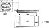
图14A示出了有源矩阵显示设备的框图的实例。像素部分5301、第一扫描线驱动电路5302、第二扫描线驱动电路5303和信号线驱动电路5304被设置于显示设备内的基板5300之上。在像素部分5301内,布置有从信号线驱动电路5304延伸出的多条信号线,以及布置有从第一扫描线驱动电路5302和第二扫描线驱动电路5303延伸出的多条扫描线。注意,各自包括显示元件的像素按照矩排布于其中扫描线和信号线彼此相交的各个区域内。显示设备的基板5300通过诸如FPC(柔性印制电路)之类的连接部分与时序控制电路5305(也称为控制器或控制IC)连接。FIG. 14A shows an example of a block diagram of an active matrix display device. A
在图14A中,第一扫描线驱动电路5302、第二扫描线驱动电路5303和信号线驱动电路5304形成于其中形成了像素部分5301的基板5300之上。因此,在外部提供的驱动电路等的构件的数量得以减少,从而能够降低成本。而且,能够减少在基板5300与外部驱动电路之间的连接部分(例如,FPC)的数量,并且能够提高可靠性或产量。In FIG. 14A, a first scan
注意,时序控制电路5305将第一扫描线驱动电路起始信号(GSP1)(起始信号也称为起始脉冲)以及扫描线驱动电路时钟信号(GCK1)供应给第一扫描线驱动电路5302。而且,时序控制电路5305将第二扫描线驱动电路起始信号(GSP2)、扫描线驱动电路时钟信号(GCK2)等供应给第二扫描线驱动电路5303。Note that the
而且,时序控制电路5305将信号线驱动电路起始信号(SSP)、信号线驱动电路时钟信号(SCK)、视频信号数据(DATA,也简称为视频信号)、锁存信号(LAT)等供应给信号线驱动电路5304。每个时钟信号可以是具有偏移相位的多个时钟信号,或者可以与通过使时钟信号反相而获得的信号(CKB)一起来供应。注意,有可能省略第一扫描线驱动电路5302和第二扫描线驱动电路5303中的一个。Also, the
图14B示出了以下结构:具有较低的驱动频率的电路(例如,第一扫描线驱动电路5302和第二扫描线驱动电路5303)形成于其上形成了像素部分5301的基板5300之上,而信号线驱动电路5304形成于与其上形成了像素部分5301的基板5300不同的基板之上。以这种结构,即使在使用其场效应迁移率相对较低的晶体管的情况下,某些驱动电路也能够形成于其上形成了像素部分5301的基板5300之上。因而,能够实现成本降低、产量提高等。14B shows a structure in which a circuit having a lower driving frequency (for example, a first scanning
然后,由n沟道晶体管构成的信号线驱动电路的结构及操作的实例将参照图15A和15B来描述。Then, an example of the structure and operation of a signal line driver circuit composed of n-channel transistors will be described with reference to FIGS. 15A and 15B.
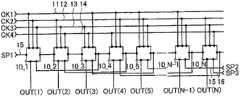
信号线驱动电路包括移位寄存器5601和开关电路5602。开关电路5602由开关电路5602_1到5602_N(N是自然数)构成。开关电路5602_1到560_2N各自由晶体管5603_1到5603_k(k是自然数)构成。在此,晶体管5603_1到5603_k是n沟道晶体管。The signal line driving circuit includes a
在信号线驱动电路内的连接关系通过将开关电路5602_1用作实例来描述。晶体管5603_1到5603_k的第一端子分别与布线5604_1到5604_k连接。晶体管5603_1到5603_k的第二端子分别与信号线S1到Sk连接。晶体管5603_1到5603_k的栅极与布线5605_1连接。The connection relationship within the signal line driver circuit is described by using the switch circuit 5602_1 as an example. First terminals of the transistors 5603_1 to 5603_k are connected to wirings 5604_1 to 5604_k, respectively. The second terminals of the transistors 5603_1 to 5603_k are connected to the signal lines S1 to Sk, respectively. The gates of the transistors 5603_1 to 5603_k are connected to the wiring 5605_1.
移位寄存器5601具有通过将H电平信号(也称为H信号或者处于高电源电位电平的信号)依次输出到布线5605_1到5605_N来依次选择开关电路5602_1到5602_N的功能。The
开关电路5602_1具有控制在布线5604_1到5604_k与信号线S1到Sk之间的导通状态(在第一端子与第二端子之间的电连续性)的功能,也就是,控制是否将布线5604_1到5604_k的电位供应给信号线S1到Sk的功能。以这种方式,开关电路5602_1起着选择器的作用。而且,晶体管5603_1到5603_k具有分别控制在布线5604_1到5604_k与信号线S1到Sk之间的导通状态的功能,也就是,分别控制是否将布线5604_1到5604_k的电位供应给信号线S1到Sk的功能。以这种方式,晶体管5603_1到5603_k每个都起着开关的作用。The switch circuit 5602_1 has a function of controlling the conduction state (electrical continuity between the first terminal and the second terminal) between the wirings 5604_1 to 5604_k and the signal lines S1 to Sk, that is, controls whether to connect the wirings 5604_1 to 5604_k to The potential of 5604_k is supplied to the functions of the signal lines S1 to Sk. In this way, the switch circuit 5602_1 functions as a selector. Also, the transistors 5603_1 to 5603_k have functions of controlling conduction states between the wirings 5604_1 to 5604_k and the signal lines S1 to Sk, respectively, that is, respectively controlling whether or not the potentials of the wirings 5604_1 to 5604_k are supplied to the signal lines S1 to Sk. Function. In this way, each of the transistors 5603_1 to 5603_k functions as a switch.
视频信号数据(DATA)被输入每条布线5604_1到5604_k。视频信号数据(DATA)通常是对应于图像数据或图像信号的模拟信号。Video signal data (DATA) is input to each of the wirings 5604_1 to 5604_k. Video signal data (DATA) is generally an analog signal corresponding to image data or image signals.
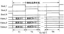
然后,参照图15B中的时序图来描述在图15A中的信号线驱动电路的操作。图15B示出了信号Sout_1到Sout_N以及信号Vdata_1到Vdata_k的实例。信号Sout_1到Sout_N是移位寄存器5601的输出信号的实例。信号Vdata_1到Vdata_k是输入布线5604_1到5604_k的信号的实例。注意,在显示设备中,信号线驱动电路的一个操作时段对应于一个栅极选择时段。例如,一个栅极选择时段被划分成时段T1到TN。每个时段T1到TN是用于将视频信号数据(DATA)写入属于所选行的像素之内的时段。Then, the operation of the signal line driver circuit in FIG. 15A is described with reference to the timing chart in FIG. 15B. FIG. 15B shows an example of signals Sout_1 to Sout_N and signals Vdata_1 to Vdata_k. Signals Sout_1 through Sout_N are examples of output signals of the
注意,在本实施例的附图中的信号波形失真等在某些情况下为了简明起见而放大。因此,本实施例并不必要限定于附图所示的比例。Note that signal waveform distortion and the like in the drawings of the present embodiment are exaggerated for clarity in some cases. Therefore, the present embodiment is not necessarily limited to the scale shown in the drawings.
在时段T1到TN内,移位寄存器5601将H电平信号按顺序输出到布线5605_1到5605_N。例如,在时段T1内,移位寄存器5601将高电平信号输出到布线5605_1。此时,晶体管5603_1到5603_k被开启,从而使布线5604_1到5604_k以及信号线S1到Sk变为导通。然后,Data(S1)到Data(Sk)分别被输入布线5604_1到5604_k。Data(S1)到Data(Sk)分别通过晶体管5603_1到5603_k写入所选行内的第一到第k列中的像素之内。以这样的方式,在时段T1到TN内,视频信号数据(DATA)按顺序逐k列地写入所选行中的像素之内。During periods T1 to TN, the
如同以上所描述的那样,视频信号数据(DATA)按照多列的方式写入像素之内,由此能够减少视频信号数据(DATA)的数量或者布线的数量。因此,能够减少与外部电路连接的数量。而且,当视频信号按照多列的方式写入像素之内时,能够延长写入的时间;因而,能够防止视频信号写入不充分。As described above, the video signal data (DATA) is written into pixels in columns, whereby the number of video signal data (DATA) or the number of wirings can be reduced. Therefore, the number of connections to external circuits can be reduced. Furthermore, when video signals are written into pixels in multiple columns, the writing time can be extended; thus, insufficient video signal writing can be prevented.
注意,由实施例1和2中的晶体管构成的任何电路都能够用于移位寄存器5601和开关电路5602。在这种情况下,移位寄存器5601能够仅由单极晶体管来构成。Note that any circuit composed of transistors in
然后,将描述扫描线驱动电路的结构。扫描线驱动电路包括移位寄存器。另外,扫描线驱动电路在某些情况下还可以包括电平移位器、缓冲器等。在扫描线驱动电路中,时钟信号(CLK)和起始脉冲信号(SP)被输入移位寄存器,从而生成选择信号。所生成的选择信号由缓冲器来缓冲和放大,并且所产生的信号被供应给相应的扫描线。在一条线路的像素内的晶体管的栅极电极与扫描线连接。由于在一条线路的像素内的晶体管必须全部同时开启,因而使用能够供应大电流的缓冲器。Then, the structure of the scanning line driver circuit will be described. The scan line driving circuit includes a shift register. In addition, the scan line driving circuit may further include a level shifter, a buffer, and the like in some cases. In the scanning line driving circuit, a clock signal (CLK) and a start pulse signal (SP) are input to a shift register, thereby generating a selection signal. The generated selection signal is buffered and amplified by the buffer, and the generated signal is supplied to the corresponding scan line. The gate electrodes of the transistors in the pixels of one line are connected to the scanning line. Since the transistors in the pixels of one line must all be turned on at the same time, a buffer capable of supplying a large current is used.
用于扫描线驱动电路和/或信号线驱动电路的一部分的移位寄存器的一个实施例将参照图16A到16D及图17A和17B来描述。One embodiment of a shift register used for a part of a scan line driver circuit and/or a signal line driver circuit will be described with reference to FIGS. 16A to 16D and FIGS. 17A and 17B.
移位寄存器包括第一到第N脉冲输出电路10_1到10_N(N是大于或等于3的自然数)(参见图16A)。在移位寄存器中,第一时钟信号CK1、第二时钟信号CK2、第三时钟信号CK3及第四时钟信号CK4分别由第一布线11、第二布线12、第三布线13及第四布线14供应给第一到第N脉冲输出电路10_1到10_N。The shift register includes first to Nth pulse output circuits 10_1 to 10_N (N is a natural number greater than or equal to 3) (see FIG. 16A ). In the shift register, the first clock signal CK1, the second clock signal CK2, the third clock signal CK3, and the fourth clock signal CK4 are connected by the
起始脉冲SP1(第一起始脉冲)由第五布线15输出到第一脉冲输出电路10_1。来自前一级的脉冲输出电路的信号(该信号被称为前级信号OUT(n-1))被输入第二或后续级的第n脉冲输出电路10_n(n是大于或等于2且小于或等于N的自然数)。The start pulse SP1 (first start pulse) is output from the
来自下一级的后级的第三脉冲输出电路10_3的信号被输入第一脉冲输出电路10_1。以类似的方式,来自下一级的后级的第(n+2)脉冲输出电路10_(n+2)的信号(该信号被称为后续级信号OUT(n+2))被输入第二或后续级的第n脉冲输出电路10_n。A signal from the third pulse output circuit 10_3 of the next subsequent stage is input to the first pulse output circuit 10_1. In a similar manner, a signal from the (n+2)th pulse output circuit 10_(n+2) of the subsequent stage of the next stage (this signal is referred to as the subsequent stage signal OUT(n+2)) is input to the second Or the nth pulse output circuit 10_n of the subsequent stage.
因而,各级的脉冲输出电路输出待输入后续级的脉冲输出电路和/或先前级的脉冲输出电路的第一输出信号(OUT(1)(SR)到OUT(N)(SR)),以及待输入不同的电路等的第二输出信号(OUT(1)到OUT(N))。注意,由于后续级信号OUT(n+2)没有被输入移位寄存器的最后两级,如图16A所示,因而第二起始脉冲SP2和第三起始脉冲SP3可以例如分别另外输入最后级的前级和最后级。Thus, the pulse output circuits of each stage output the first output signals (OUT(1)(SR) to OUT(N)(SR)) to be input to the pulse output circuits of the subsequent stage and/or the pulse output circuits of the previous stage, and Second output signals (OUT(1) to OUT(N)) of different circuits or the like are to be input. Note that since the subsequent stage signal OUT(n+2) is not input to the last two stages of the shift register, as shown in FIG. 16A, the second start pulse SP2 and the third start pulse SP3 may be additionally input to the last stage, respectively the preceding and final stages.
注意,时钟信号(CK)是按照固定的时间间隔在H电平和L电平(也称为L信号或处于低电源电位电平的信号)之间交替的信号。在此,第一时钟信号(CK1)到第四时钟信号(CK4)依次延迟1/4周期。在本实施例中,脉冲输出电路的驱动以第一到第四时钟信号(CK1)到(CK4)来控制。注意,时钟信号在某些情况下也称为GCK或SCK,取决于该时钟信号所输入的驱动电路;在以下的描述中,时钟信号被称为CK。Note that the clock signal (CK) is a signal that alternates between H level and L level (also referred to as an L signal or a signal at a low power supply potential level) at fixed time intervals. Here, the first clock signal ( CK1 ) to the fourth clock signal ( CK4 ) are sequentially delayed by 1/4 cycle. In this embodiment, the driving of the pulse output circuit is controlled with the first to fourth clock signals (CK1) to (CK4). Note that the clock signal is also called GCK or SCK in some cases, depending on the drive circuit to which the clock signal is input; in the following description, the clock signal is called CK.
第一输入端子21、第二输入端子22及第三输入端子23电连接至第一到第四布线11到14中的任意一条布线。例如,在图16A中的第一脉冲输出电路10_1内,第一输入端子21与第一布线11电连接,第二输入端子22与第二布线12电连接,而第三输入端子23与第三布线13电连接。在第二脉冲输出电路10_2中,第一输入端子21与第二布线12电连接,第二输入端子22与第三布线13电连接,而第三输入端子23与第四布线14电连接。The
假定第一到第n脉冲输出电路10_1到10_N每个都包括第一输入端子21、第二输入端子22、第三输入端子23、第四输入端子24、第五输入端子25、第一输出端子26和第二输出端子27(参见图16B)。Assume that the first to nth pulse output circuits 10_1 to 10_N each include a
在第一脉冲输出电路10_1中,第一时钟信号CK1被输入第一输入端子21;第二时钟信号CK2被输入第二输入端子22;第三时钟信号CK3被输入第三输入端子23;起始脉冲被输入第四输入端子24;后续级信号OUT(3)被输入第五输入端子25;第一输出信号OUT(1)(SR)由第一输出端子26输出;以及第二输出信号OUT(1)由第二输出端子27输出。In the first pulse output circuit 10_1, the first clock signal CK1 is input to the
在第一到第n脉冲输出电路10_1到10_N中,除了具有三个端子的晶体管之外,还能够使用具有四个端子的晶体管28(参见图16C)。注意,在本说明书中,当晶体管具有两个栅极电极(半导体层在它们之间)时,在半导体层下方的栅极电极称为下栅极电极,而在半导体层上方的栅极电极称为上栅极电极。晶体管28是能够以输入下栅极电极的第一控制信号G1以及输入上栅极电极的第二控制信号G2来执行在IN端子与OUT端子之间的电控制的元件。In the first to nth pulse output circuits 10_1 to 10_N, in addition to transistors having three terminals,
当氧化物半导体被用于晶体管中包括沟道形成区的半导体层时,阈值电压有时沿正或负方向偏移,取决于制造过程。由于该原因,其中氧化物半导体被用于包括沟道形成区的半导体层的晶体管优选地具有能够用来控制阈值电压的结构。在图16C中,栅极电极被设置于晶体管28的沟道形成区之上和之下,栅极绝缘层在它们之间。通过控制上栅极电极和/或下栅极电极的电位,能够控制阈值电压使之为所期望的值。When an oxide semiconductor is used for a semiconductor layer including a channel formation region in a transistor, the threshold voltage sometimes shifts in a positive or negative direction, depending on the manufacturing process. For this reason, a transistor in which an oxide semiconductor is used for a semiconductor layer including a channel formation region preferably has a structure that can be used to control a threshold voltage. In FIG. 16C , gate electrodes are provided above and below the channel formation region of the
然后,将参照图16D来描述脉冲输出电路的特定电路配置的实例。Then, an example of a specific circuit configuration of the pulse output circuit will be described with reference to FIG. 16D.
在图16D中所示出的脉冲输出电路包括第一到第十三晶体管31到43。第一到第十三晶体管31到43连接至第一到第五输入端子21到25、第一输出端子26、第二输出端子27、对其供应第一高电源电位VDD的电源线51、对其供应第二高电源电位VCC的电源线52以及对其供应低电源电位VSS的电源线53。除了第一到第五输入端子21到25、第一输出端子26以及第二输出端子27之外,信号或电源电位还由供应第一高电源电位VDD的电源线51、供应第二高电源电位VCC的电源线52以及供应低电源电位VSS的电源线53供应给第一到第十三晶体管31到43。The pulse output circuit shown in FIG. 16D includes first to
在图16D中的电源线的电源电位的关系如下:第一电源电位VDD高于或等于第二电源电位VCC,以及第二电源电位VCC高于第三电源电位VSS。注意,第一到第四时钟信号(CK1)到(CK4)每个都按照固定的时间间隔在H电平与L电平之间交替;例如,处于H电平的时钟信号是VDD以及处于L电平的时钟信号为VSS。The relationship of the power supply potentials of the power supply lines in FIG. 16D is as follows: the first power supply potential VDD is higher than or equal to the second power supply potential VCC, and the second power supply potential VCC is higher than the third power supply potential VSS. Note that each of the first to fourth clock signals (CK1) to (CK4) alternates between H level and L level at fixed time intervals; for example, the clock signal at H level is VDD and at L level. The level of the clock signal is VSS.
通过使电源线51的电位VDD变得比电源线52的电位VCC高,能够降低施加于晶体管的栅极电极的电位,能够减小晶体管的阈值电压的偏移,并且能够抑制晶体管的劣化,而对晶体管的操作没有不利影响。By making the potential VDD of the
如图16D所示,在图16C中具有四个端子的晶体管28优选地被用作在第一到第十三晶体管31到43当中的第一晶体管31和第六到第九晶体管36到39中的每个晶体管。As shown in FIG. 16D, a
与用作第一晶体管31和第六到第九晶体管36到39中的每个晶体管的源极或漏极的一个电极连接的节点的电位需要用第一晶体管31和第六到第九晶体管36到39中的每个晶体管的栅极电极的控制信号来切换。此外,由于对于输入栅极电极的控制信号的相应快速(通态电流的上升急剧),因而第一晶体管31和第六到第九晶体管36到39各自优选地减少了脉冲输出电路的故障。因而,通过使用具有四个端子的晶体管,能够控制阈值电压,并且能够进一步减少脉冲输出电路的故障。注意,在图16D中,第一控制信号G1和第二控制信号G2是相同的控制信号;但是,可以输入不同的控制信号。The potential of the node connected to one electrode serving as the source or drain of each of the
在图16D中,第一晶体管31的第一端子与电源线51电连接,第一晶体管31的第二端子与第九晶体管39的第一端子电连接,以及第一晶体管31的栅极电极(下栅极电极和上栅极电极)与第四输入端子24电连接。In FIG. 16D, the first terminal of the
第二晶体管32的第一端子与电源线53电连接,第二晶体管32的第二端子与第九晶体管39的第一端子电连接,以及第二晶体管32的栅极电极与第四晶体管34的栅极电极电连接。The first terminal of the
第三晶体管33的第一端子与第一输入端子21电连接,以及第三晶体管33的第二端子与第一输出端子26电连接。A first terminal of the
第四晶体管34的第一端子与电源线53电连接,以及第四晶体管34的第二端子与第一输出端子26电连接。A first terminal of the
第五晶体管35的第一端子与电源线53电连接,第五晶体管35的第二端子与第二晶体管32的栅极电极以及第四晶体管34的栅极电极电连接,以及第五晶体管35的栅极电极与第四输入端子24电连接。The first terminal of the
第六晶体管36的第一端子与电源线52电连接,第六晶体管36的第二端子与第二晶体管32的栅极电极以及第四晶体管34的栅极电极电连接,以及第六晶体管36的栅极电极(下栅极电极和上栅极电极)与第五输入端子25电连接。The first terminal of the
第七晶体管37的第一端子与电连接电源线52,第七晶体管37的第二端子与第八晶体管38的第二端子电连接,以及第七晶体管37的栅极电极(下栅极电极和上栅极电极)与第三输入端子23电连接。The first terminal of the
第八晶体管38的第一端子与第二晶体管32的栅极电极以及第四晶体管34的栅极电极电连接,以及第八晶体管38的栅极电极(下栅极电极和上栅极电极)与第二输入端子22电连接。The first terminal of the
第九晶体管39的第一端子与第一晶体管31的第二端子以及第二晶体管32的第二端子电连接,第九晶体管39的第二端子与第三晶体管33的栅极电极以及第十晶体管40的栅极电极电连接,以及第九晶体管39的栅极电极(下栅极电极和上栅极电极)与电源线52电连接。The first terminal of the
第十晶体管40的第一端子与第一输入端子21电连接,第十晶体管40的第二端子与第二输出端子27电连接,以及第十晶体管40的栅极电极与第九晶体管39的第二端子电连接。The first terminal of the
第十一晶体管41的第一端子与电源线53电连接,第十一晶体管41的第二端子与第二输出端子27电连接,以及第十一晶体管41的栅极电极与第二晶体管32的栅极电极以及第四晶体管34的栅极电极电连接。The first terminal of the
第十二晶体管42的第一端子与电源线53电连接,第十二晶体管42的第二端子与第二输出端子27电连接,以及第十二晶体管42的栅极电极与第七晶体管37的栅极电极(下栅极电极和上栅极电极)电连接。The first terminal of the
第十三晶体管43的第一端子与电源线53电连接,第十三晶体管43的第二端子与第一输出端子26电连接,以及第十三晶体管43的栅极电极与第七晶体管37的栅极电极(下栅极电极和上栅极电极)电连接。The first terminal of the
在图16D中,第三晶体管33的栅极电极、第十晶体管40的栅极电极以及第九晶体管39的第二端子相连接的部分被称为节点A。而且,第二晶体管32的栅极电极、第四晶体管34的栅极电极、第五晶体管35的第二端子、第六晶体管36的第二端子、第八晶体管38的第一端子以及第十一晶体管41的栅极电极相连接的部分被称为节点B(参见图17A)。In FIG. 16D , a portion where the gate electrode of the
图17A示出了在图16D所示的脉冲输出电路被应用于第一脉冲输出电路10_1的情况下被输入第一到第五输入端子21到25以及第一和第二输出端子26和27的或者由其所输出的信号。FIG. 17A shows the pulses input to the first to
具体地,第一时钟信号CK1输入第一输入端子21;第二时钟信号CK2输入第二输入端子22;第三时钟信号CK3输入第三输入端子23;起始脉冲(SP1)输入第四输入端子24;后续级信号OUT(3)输入第五输入端子25;第一输出信号OUT(1)(SR)由第一输出端子26输出;以及第二输出信号OUT(1)由第二输出端子27输出。Specifically, the first clock signal CK1 is input to the
注意,晶体管是具有至少三个端子(栅极、漏极和源极)的元件,其中沟道区形成于漏极区与源极区之间,并且电流能够流过漏极区、沟道区及源极区。在此,由于晶体管的源极和漏极可以改变,取决于晶体管的结构、操作条件等,因而难以界定哪个是源极或漏极。因此,在某些情况下起着源极或漏极的作用的区域不称为源极或漏极。在这种情况下,例如,此类区域可以称为第一端子和第二端子。Note that a transistor is an element having at least three terminals (gate, drain, and source), wherein a channel region is formed between the drain region and the source region, and current can flow through the drain region, the channel region and the source region. Here, since the source and drain of the transistor can vary depending on the structure of the transistor, operating conditions, etc., it is difficult to define which is the source or the drain. Therefore, a region that functions as a source or a drain in some cases is not called a source or a drain. In this case, for example, such regions may be referred to as a first terminal and a second terminal.
注意,在图17A中,可以另外提供用于通过使节点进入浮置状态来执行自举操作的电容器。而且,可以另外提供具有一个与节点B电连接的电极的电容器,以便保持节点B的电位。Note that, in FIG. 17A , a capacitor for performing a bootstrap operation by bringing a node into a floating state may be additionally provided. Also, a capacitor having an electrode electrically connected to the node B may be additionally provided in order to maintain the potential of the node B.
图17B示出了包括图17A所示的多个脉冲输出电路的移位寄存器的时序图。注意,当移位寄存器是扫描线驱动电路之一时,在图17B中的时段61对应于垂直折回时段,以及时段62对应于栅极选择时段。FIG. 17B shows a timing chart of a shift register including a plurality of pulse output circuits shown in FIG. 17A. Note that when the shift register is one of the scanning line driving circuits, a period 61 in FIG. 17B corresponds to a vertical wrapping period, and a period 62 corresponds to a gate selection period.
注意,其中第二电源电位VCC如图17A所示出的那样被施加于栅极电极的第九晶体管39的布置在自举操作之前和之后具有下列优点。Note that the arrangement of the
没有其中第二电源电位VCC被施加于栅极电极的第九晶体管39,如果节点的电位由自举操作来提升,则作为第一晶体管31的第二端子的源极的电位会上升至高于第一电源电位VDD的值。然后,第一晶体管31的源极被切换至第一端子,也就是,在电源线51一侧的端子。因此,在第一晶体管31中,高偏压电压被施加,并因而显著的应力被施加于栅极与源极之间以及于栅极与漏极之间,这可能导致晶体管劣化。Without the
另一方面,以其中第二电源电位VCC被施加于栅极电极的第九晶体管39,能够防止第一晶体管31的第二端子的电位上升,而节点的电位通过自举操作来提升。换言之,第九晶体管39的布置能够降低施加于第一晶体管31的栅极与源极之间的负偏压电压的电平。因而,在本实施例中的电路配置能够降低施加于第一晶体管31的栅极与源极之间的负偏压电压,从而能够抑制因应力所致的第一晶体管31的劣化。On the other hand, with the
注意,可以提供第九晶体管39,使得第九晶体管39的第一端子和第二端子连接于第一晶体管31的第二端子与第三晶体管33的栅极之间。注意,在与扫描线驱动电路相比具有更多数量的级的信号线驱动电路中,在移位寄存器包括本实施例的多个脉冲输出电路的情况下,能够省略第九晶体管39,则有利于减少晶体管的数量。Note that the
注意,氧化物半导体被用于第一到第十三晶体管31到43中的每个晶体管的半导体层,由此能够降低晶体管的断态电流,能够提高通态电流和场效应迁移率。因此,能够降低晶体管的劣化程度,并从而减少电路的故障。而且,通过将高电位施加于栅极电极而使用氧化物半导体的晶体管的劣化程度使用小于使用非晶硅的晶体管的劣化程度。因此,即使在将第一电源电位VDD供应给供应第二电源电位VCC的电源线时也能够获得相似的操作,并且能够减少布置于电路之间的电源线的数量;因而,能够减小电路的尺寸。Note that an oxide semiconductor is used for the semiconductor layer of each of the first to
注意,即使在连接关系被改变,使得由第三输入端子23供应给第七晶体管37的栅极电极(下栅极电极和上栅极电极)的时钟信号以及由第二输入端子22供应给第八晶体管38的栅极电极(下栅极电极和上栅极电极)的时钟信号分别由第二输入端子22和第三输入端子23来供应时,也获得相似的功能。Note that even when the connection relationship is changed so that the clock signal supplied to the gate electrode (the lower gate electrode and the upper gate electrode) of the
在图17A所示的移位寄存器中,第七晶体管37和第八晶体管38的状态被改变,使得第七晶体管37和第八晶体管38两者都导通,然后第七晶体管37截止而第八晶体管38导通,以及然后第七晶体管37和第八晶体管38都截止;因而,由第七晶体管37的栅极电极的电位下降以及第八晶体管38的栅极电极的电位下降而两度导致因第二输入端子22和第三输入端子23的电位下降所致的节点B的电位下降。In the shift register shown in FIG. 17A, the states of the
另一方面,在图17A所示的移位寄存器中,当第七晶体管37和第八晶体管38的状态被改变,使得第七晶体管37和第八晶体管38两者都导通,然后第七晶体管37导通而第八晶体管38截止,以及然后第七晶体管37和第八晶体管38都截止时,因第二输入端子22和第三输入端子23的电位下降所致的节点B的电位下降仅发生一次,其中此次电位下降是由第八晶体管38的栅极电极的电位下降所导致的。On the other hand, in the shift register shown in FIG. 17A, when the states of the
因此,以下连接关系是优选的:时钟信号CK3由第三输入端子23供应给第七晶体管37的栅极电极(下栅极电极和上栅极电极)以及时钟信号CK2由第二输入端子22供应给第八晶体管38的栅极电极(下栅极电极和上栅极电极)。这是因为能够减少节点B的电位的改变次数,由此能够减少噪声。Therefore, the following connection relationship is preferable: the clock signal CK3 is supplied from the
以这样的方式,H电平信号在第一输出端子26和第二输出端子27的电位被保持于L电平的时段内被有规律地供应给节点B;因而,能够抑制脉冲输出电路的故障。In this way, the H level signal is regularly supplied to the node B during the period in which the potentials of the
注意,本实施例所描述的结构能够适当地结合其它实施例所描述的任何结构来使用。Note that the structure described in this embodiment can be used in combination with any structures described in other embodiments as appropriate.
(实施例4)(Example 4)
在本实施例中,将描述通过将实施例1和2所描述的晶体管用于像素部分和驱动电路内而形成的具有显示功能的显示设备。In this embodiment, a display device having a display function formed by using the transistors described in
显示设备包括显示元件。作为显示元件,能够使用液晶元件(也称为液晶显示元件)或发光元件(也称为发光显示元件)。在其种类中,发光元件包括其亮度通过电流或电压来控制的元件,具体地,包括无机电致发光(EL)元件、有机EL元件等。而且,能够使用其对比度通过电效应来改变的显示介质,例如,电子墨水。The display device includes a display element. As a display element, a liquid crystal element (also called a liquid crystal display element) or a light emitting element (also called a light emitting display element) can be used. Among its categories, light emitting elements include elements whose luminance is controlled by current or voltage, specifically, inorganic electroluminescence (EL) elements, organic EL elements, and the like. Also, it is possible to use a display medium whose contrast is changed by an electric effect, for example, electronic ink.
注意,本说明书中的显示设备指的是图像显示设备、显示设备或光源(包括照明设备)。此外,显示设备在其种类中包括下列模块:包括诸如柔性印制电路(FPC)、带式自动接合(TAB)卷带之类的连接器的模块;具有在其末端设置有印制布线板的TAB卷带的模块;以及具有以玻璃上芯片(COG)方法直接安装于显示元件上的集成电路(IC)的模块。Note that a display device in this specification refers to an image display device, a display device, or a light source (including a lighting device). In addition, the display device includes the following modules in its category: a module including a connector such as a flexible printed circuit (FPC), a tape automated bonding (TAB) reel; a module having a printed wiring board provided at its end; A module of TAB tape; and a module with an integrated circuit (IC) mounted directly on a display element in a chip-on-glass (COG) method.
在本实施例中,将参照图20A1、20A2及20B来描述作为半导体设备的一种实施例的液晶显示屏的外观和截面。图20A1和20A2是液晶显示屏的顶视平面图。图20B是沿着图20A1和20A2中的M-N的截面图。液晶显示屏具有以下结构:液晶元件4013以密封剂4005密封于设置有各自包括氧化物半导体层的晶体管4010和4011的第一基板4001与第二基板4006之间。In this embodiment, the appearance and cross-section of a liquid crystal display as an example of a semiconductor device will be described with reference to FIGS. 20A1, 20A2, and 20B. 20A1 and 20A2 are top plan views of liquid crystal displays. Fig. 20B is a sectional view along M-N in Figs. 20A1 and 20A2. The liquid crystal display has a structure in which a
密封剂4005被这样提供使得包围设置于第一基板4001之上的像素部分4002和扫描线驱动电路4004。第二基板4006被设置于像素部分4002和扫描线驱动电路4004之上。因此,像素部分4002和扫描线驱动电路4004与液晶层4008一起由第一基板4001、密封剂4005及第二基板4006来密封。使用单晶半导体或多晶半导体形成的信号线驱动电路4003被安装于与在第一基板4001之上的由密封剂4005包围的区域不同的区域内。The
注意,对于单独形成的驱动电路的连接方法没有特别的限制,并且能够使用COG法、丝线键合法、TAB法等。图20A1示出了以COG法来安装信号线驱动电路4003的实例。图20A2示出了以TAB法来安装信号线驱动电路4003的实例。Note that there is no particular limitation on the connection method of the separately formed drive circuits, and a COG method, a wire bonding method, a TAB method, or the like can be used. FIG. 20A1 shows an example of mounting the signal
设置于第一基板4001之上的像素部分4002和扫描线驱动电路4004包括多个晶体管。作为实例,图20B示出了包含于像素部分4002内的晶体管4010以及包含于扫描线驱动电路4004内的晶体管4011。绝缘层4020和4021被设置于晶体管4010之上,而绝缘层4020被设置于晶体管4011之上。The
实施例1和2所描述的包含氧化物半导体层的任何高可靠性的晶体管都能够用作晶体管4010和4011。在本实施例中,晶体管4010和4011是n沟道晶体管。Any highly reliable transistor including an oxide semiconductor layer described in
导电层4040被设置于绝缘层4044的一部分之上,该导电层4040与在晶体管4011内用于驱动电路的氧化物半导体层的沟道形成区重叠。导电层4040被设置于与氧化物半导体层的沟道形成区重叠的位置,由此能够降低晶体管的阈值电压4011在BT测试前后之间的变化量。导电层4040的电位是与晶体管4011的栅极电极层的电位相同的,由此导电层4040能够起着第二栅极电极层的作用。作为选择,导电层4040可以是与晶体管4011的栅极电极层的电位不同的给定电位。仍然,作为选择,导电层4040的电位可以是GND或0V,或者导电层4040可以处于浮置状态。A
包含于液晶元件4013内的像素电极层4030与晶体管4010电连接。液晶元件4013的对电极层4031形成于第二基板4006上。像素电极层4030、对电极层4031及液晶层4008相互重叠的部分对应于液晶元件4013。像素电极层4030和对电极层4031分别设置有起着对准膜的作用的绝缘层4032和绝缘层4033。注意,虽然没有示出,但是可以将彩色滤光片设置于第一基板4001一侧或者于第二基板4006一侧。The
注意,玻璃、陶瓷或塑料能够用作第一基板4001和第二基板4006。作为塑料,能够使用玻璃纤维增强塑料(FRP)板、聚氟乙烯(PVF)膜、聚酯膜或丙烯酸树脂膜。作为选择,可以使用具有其中铝箔夹在PVF膜、聚酯膜等之间的结构的薄片。Note that glass, ceramics, or plastic can be used as the
柱状隔件4035被提供以便控制液晶层4008的厚度(单元间隙)。柱状隔件4035通过绝缘膜的选择性蚀刻来获得。作为选择,可以使用球形隔件。
对电极层4031与形成于其内形成了晶体管4010的基板之上的公共电位线电连接。对电极层4031和公共电位线能够通过布置于使用公共连接部分的一对基板之间的导电粒子来相互电连接。注意,导电粒子包含于密封剂4005内。The
作为选择,可以使用展现出不需要对准膜的蓝相的液晶。蓝相是一种液晶相,该液晶相仅于胆甾相在胆甾液晶的温度增加的同时改变成各向同性相之前产生。由于蓝相仅在窄小的温度范围内产生,因而将含有重量百分比为5%或更高的手性剂的液晶组成用于液晶层4008,以便增大温度范围。包含展现出蓝相的液晶和手性剂的液晶组成具有10-100μsec的短的响应时间,并且是光学各向同性的;因此,不需要对准处理并且视角依赖性是小的。注意,在使用蓝相的情况下,本发明的实施例并不限于图20A1、20A2及20B中的结构,而是可以使用所谓的水平电场模式的结构,在该结构中,与对电极层4031对应的电极层形成于其上形成了像素电极层4030的基板的侧面上。Alternatively, a liquid crystal exhibiting a blue phase that does not require an alignment film may be used. The blue phase is a liquid crystal phase which is generated only before the cholesteric phase is changed into an isotropic phase while the temperature of the cholesteric liquid crystal is increased. Since the blue phase is generated only in a narrow temperature range, a liquid crystal composition containing 5% by weight or more of a chiral agent is used for the
注意,本实施例是透射液晶显示设备的实例,并且同样能够应用于反射液晶显示设备和透反液晶显示设备。Note that the present embodiment is an example of a transmissive liquid crystal display device, and can be equally applied to a reflective liquid crystal display device and a transflective liquid crystal display device.
在根据本实施例的液晶显示设备的实例中,偏光板设置于基板的外表面上(在观看者一侧),以及用于显示元件的着色层和电极层依次设置于基板的内表面上;作为选择,偏光板可以设置于基板的内表面上。偏光板和着色层的层状结构并不限于本实施例中的结构,而是可以根据偏光板和着色层的材料或者制造过程的条件适当地设定。此外,还可以设置用作黑色基质的阻光膜。In an example of the liquid crystal display device according to the present embodiment, the polarizing plate is provided on the outer surface of the substrate (on the viewer's side), and the coloring layer and the electrode layer for the display element are sequentially provided on the inner surface of the substrate; Alternatively, a polarizing plate may be provided on the inner surface of the substrate. The layered structure of the polarizing plate and the colored layer is not limited to the structure in this embodiment, but can be appropriately set according to the materials of the polarizing plate and the colored layer or the conditions of the manufacturing process. In addition, a light blocking film serving as a black matrix may also be provided.
在本实施例中,为了降低因晶体管所致的表面粗糙度以及提高可靠性,晶体管以用作保护膜和平面化绝缘膜的绝缘层(绝缘层4020和4021)来覆盖。注意,保护膜被提供用于防止存在于空气中的诸如有机物质、金属及湿气之类的污染杂质进入,并且优选为致密膜。保护膜可以用使用氧化硅膜、氮化硅膜、氧氮化硅膜、氮氧化硅膜、氧化铝膜、氮化铝膜、氧氮化铝膜及氮氧化铝膜中的任何种的单层结构或层状结构来形成。虽然本实施例描述了其中保护膜以溅射法来形成的实例,但是任何其它方法都可以使用。In this embodiment, in order to reduce surface roughness due to transistors and improve reliability, transistors are covered with insulating layers (insulating
在本实施例中,具有层状结构的绝缘层4020被形成为保护膜。在此,氧化硅膜以溅射法形成为绝缘层4020的第一层。将氧化硅膜用作保护膜具有防止用作源极和漏极电极层的铝膜的凸起的效果。In this embodiment, an insulating
此外,作为保护膜的第二层,氮化硅膜以溅射法形成。将氮化硅膜用作保护膜能够防止钠等可动离子进入半导体区,从而能够抑制晶体管的电特性的变化。In addition, as a second layer of the protective film, a silicon nitride film was formed by sputtering. Using the silicon nitride film as a protective film can prevent mobile ions such as sodium from entering the semiconductor region, thereby suppressing changes in the electrical characteristics of the transistor.
在保护膜形成之后,可以执行氧化物半导体层的退火(300℃-400℃)。After the protective film is formed, annealing (300° C. to 400° C.) of the oxide semiconductor layer may be performed.
绝缘层4021形成为平面化绝缘膜。绝缘层4021能够使用诸如丙烯酸树脂、聚酰亚胺、苯并环丁烯树脂、聚酰胺或环氧树脂之类的耐热性有机材料形成。除了此类有机材料之外,还有可能使用低介电常数的材料(低k值材料)、硅氧烷基树脂、PSG(磷硅酸盐玻璃)、BPSG(硼磷硅酸盐玻璃)等。注意,绝缘层4021可以通过堆叠使用这些材料中的任何种形成的多个绝缘膜来形成。The insulating
注意,硅氧烷基树脂是使用硅氧烷基材料作为起始材料形成的包含Si-O-Si键的树脂。硅氧烷基树脂可以包含作为取代基的有机基团(例如,烷基或芳基)或氟基。而且,有机基团可以包括氟基。Note that a siloxane-based resin is a resin containing Si-O-Si bonds formed using a siloxane-based material as a starting material. The silicone-based resin may contain an organic group (for example, an alkyl group or an aryl group) or a fluorine group as a substituent. Also, the organic group may include a fluorine group.
对于形成绝缘层4021的方法没有特别的限制,并且能够根据材料采用下列方法或装置:方法,例如,溅射法、SOG法、旋涂法、浸渍法、喷涂法或液滴释放法(例如,喷墨法、丝网印刷或胶版印刷),或者工具,例如,刮刀、辊涂机、幕涂机或刮涂机。在使用液体材料形成绝缘层4021的情况下,氧化物半导体层的退火(300℃-400℃)可以与烘焙步骤同时执行。绝缘层4021的烘焙步骤还用作氧化物半导体层的退火,由此能够减少步骤。There are no particular limitations on the method of forming the insulating
像素电极层4030和对电极层4031能够使用透光导电材料来形成,例如,含有氧化钨的氧化铟、含有氧化钨的氧化铟锌、含有氧化钛的氧化铟、含有氧化钛的氧化铟锡、氧化铟锡、氧化铟锌或者其中添加了氧化硅的氧化铟锡。The
作为选择,包含导电高分子(也称为导电聚合物)的导电组成能够用于像素电极层4030和对电极层4031。使用导电组成形成的像素电极优选具有小于或等于每平方10000欧姆的薄层电阻以及在550nm的波长下大于或等于70%的透光率。此外,包含于导电组成内的导电高分子的电阻率优选小于或等于0.1Ω·cm。Alternatively, a conductive composition including a conductive high molecule (also referred to as a conductive polymer) can be used for the
作为导电高分子,能够使用所谓的π-电子共轭型导电聚合物。实例是聚苯胺及其衍生物、聚吡咯及其衍生物、聚噻吩及其衍生物以及这些材料中的两种或更多种材料的共聚物。As the conductive polymer, a so-called π-electron conjugated conductive polymer can be used. Examples are polyaniline and its derivatives, polypyrrole and its derivatives, polythiophene and its derivatives, and copolymers of two or more of these materials.
此外,还通过FPC4018将各种信号和电位被供应给单独形成的信号线驱动电路4003、扫描线驱动电路4004或像素部分4002。In addition, various signals and potentials are also supplied to the separately formed signal
在本实施例中,连接端子电极4015使用与包含于液晶元件4013内的像素电极层4030相同的导电膜形成。端子电极4016使用与晶体管4010和晶体管4011的源极和漏极电极层相同的导电膜形成。In this embodiment, the
连接端子电极4015穿过各向异性导电膜4019与包含于FPC4018内的端子电连接。The
注意,图20A1、20A2及20B示出了其中信号线驱动电路4003安装于第一基板4001上的实例;但是,本实施例并不限于这种结构。可以仅安装扫描线驱动电路的一部分和信号线驱动电路的一部分或者扫描线驱动电路的一部分。Note that FIGS. 20A1 , 20A2 and 20B show an example in which the signal
图21示出了使用实施例1和2所描述的晶体管形成于其上的基板2600形成的液晶显示模块的实例。FIG. 21 shows an example of a liquid crystal display module formed using the
图21示出了液晶显示模块的实例,在该显示模块中,基板2600和对基板2601以密封剂2602来相互固定,并且包括晶体管等的像素部分2603、包括液晶层的显示元件2604以及着色层2605被设置于基板之间以形成显示区。着色层2605是执行彩色显示所必需的。在RGB系统中,与颜色红色、绿色和蓝色对应的着色层被提供用于像素。偏光板2606和2607以及漫射板2613被设置于基板2600和对基板2601的外部。光源包括冷阴极管2610和反射板2611。电路板2612通过柔性布线板2609与基板2600的布线电路部分2608连接,并且包括外部电路,例如,控制电路或电源电路。可以堆叠偏光板和液晶层,延迟板在它们之间。21 shows an example of a liquid crystal display module in which a
对于液晶显示模块,能够使用扭曲向列(TN)模式、共面开关(IPS)模式、边缘场开关(FFS)模式、多畴垂直取向(MVA)模式、图形化垂直取向(PVA)模式、轴对称取向微单元(ASM)模式、光学补偿双折射(OCB)模式、铁电液晶(FLC)模式、反铁电液晶(AFLC)模式等。For LCD modules, Twisted Nematic (TN) mode, In-Plane Switching (IPS) mode, Fringe Field Switching (FFS) mode, Multi-Domain Vertical Alignment (MVA) mode, Patterned Vertical Alignment (PVA) mode, Axis Symmetrically aligned microcell (ASM) mode, optically compensated birefringence (OCB) mode, ferroelectric liquid crystal (FLC) mode, antiferroelectric liquid crystal (AFLC) mode, etc.
通过以上步骤,能够形成高可靠性的液晶显示屏。Through the above steps, a highly reliable liquid crystal display can be formed.
注意,本实施例所描述的结构能够适当地结合其它实施例所描述的任何结构来使用。Note that the structure described in this embodiment can be used in combination with any structures described in other embodiments as appropriate.
(实施例5)(Example 5)
在本实施例中,电子纸的实例将作为其中应用了实施例1和2所描述的晶体管的显示设备来描述。In this embodiment, an example of electronic paper will be described as a display device in which the transistors described in
图13示出了作为显示设备的实例的有源矩阵电子纸。实施例1和2所描述的晶体管能够用作显示设备的晶体管581。FIG. 13 shows active matrix electronic paper as an example of a display device. The transistors described in
图13中的电子纸是使用扭曲球显示系统的显示设备的实例。扭曲球显示系统指的是其中各自着色为黑色和白色的球形粒子被排列于第一电极层与第二电极层之间,并且在第一电极层与第二电极层之间产生电位差以控制球形粒子的取向,从而执行显示的方法。The electronic paper in FIG. 13 is an example of a display device using a twisted ball display system. The twisted ball display system refers to a system in which spherical particles each colored in black and white are arranged between a first electrode layer and a second electrode layer, and a potential difference is generated between the first electrode layer and the second electrode layer to control Orientation of spherical particles to perform the method shown.
晶体管581是底栅晶体管,并且晶体管581的源极电极层或漏极电极层通过形成于绝缘层583、584和585内的开口与第一电极层587电连接。球形粒子589被设置于第一电极层587与第二电极层588之间。每个球形粒子589都包括黑区590a、白区590b以及在黑区590a和白区590b周围充满液体的空腔594。在球形粒子589周围的空间以诸如树脂之类的填充物595来填充(参见图13)。在本实施例中,第一电极层587对应于像素电极,以及第二电极层588对应于公共电极。第二电极层588与设置于其中形成了晶体管581的基板之上的公共电位线电连接。The
作为选择,有可能使用电泳元件来代替扭曲球。具有大约10-200μm的直径,其内封装了透明的液体、带正电的白色微粒及带负电的黑色微粒的微胶囊被使用。在设置于第一电极层与第二电极层之间的微胶囊内,当通过第一电极层和第二电极层来施加电场时,白色微粒和黑色微粒沿相反的方向移动,从而能够显示出白色或黑色。应用这种原理的显示元件是电泳显示元件,以及包括电泳显示元件的设备一般地称为电子纸。电泳显示元件与液晶显示元件相比具有更高的反射率;因而,不需要辅助光,功率消耗低,并且显示部分在昏暗的地方也能够识别。另外,即使在不给显示部分供电时,也能够维持之前已经显示的图像。因此,即使具有显示功能的显示设备(也称为半导体设备或设置有显示设备的半导体设备)远离电波源,也能够存储所显示的图像。Alternatively, it is possible to use electrophoretic elements instead of twisting balls. Microcapsules having a diameter of about 10-200 μm enclosing a transparent liquid, positively charged white particles and negatively charged black particles are used. In the microcapsules arranged between the first electrode layer and the second electrode layer, when an electric field is applied through the first electrode layer and the second electrode layer, the white particles and the black particles move in opposite directions, thereby being able to display white or black. A display element to which this principle is applied is an electrophoretic display element, and devices including the electrophoretic display element are generally called electronic paper. An electrophoretic display element has higher reflectance than a liquid crystal display element; thus, auxiliary light is not required, power consumption is low, and the display portion can be recognized in a dark place. In addition, even when power is not supplied to the display portion, an image that has been displayed before can be maintained. Therefore, even if a display device having a display function (also referred to as a semiconductor device or a semiconductor device provided with a display device) is far away from a radio wave source, a displayed image can be stored.
注意,本实施例所描述的结构能够适当地结合其它实施例所描述的任何结构来使用。Note that the structure described in this embodiment can be used in combination with any structures described in other embodiments as appropriate.
(实施例6)(Example 6)
在本实施例中,发光显示设备的实例将作为包括实施例1和2所描述的晶体管的显示设备来描述。作为包含于显示设备内的显示元件,在此描述利用电致发光的发光元件。利用电致发光的发光元件根据发光材料是有机化合物还是无机化合物来划分。一般地,前者称为有机EL元件,而后者称为无机EL元件。In this embodiment, an example of a light-emitting display device will be described as a display device including the transistors described in
在有机EL元件中,通过将电压施加于发光元件,使电子和空穴分别从一对电极注入含有发光有机化合物的层内,并且有电流流过。载流子(电子和空穴)重新结合,并因而,发光有机化合物被激发。发光有机化合物从激发态返回至基态,由此发光。因为该机制,这种发光元件被称为电流激励发光元件。In an organic EL element, by applying a voltage to a light-emitting element, electrons and holes are respectively injected from a pair of electrodes into a layer containing a light-emitting organic compound, and a current flows. The carriers (electrons and holes) recombine, and thus, the light-emitting organic compound is excited. The light-emitting organic compound returns from an excited state to a ground state, thereby emitting light. Because of this mechanism, such a light-emitting element is called a current-driven light-emitting element.
无机EL元件根据它们的元件结构划分成分散型无机EL元件和薄膜无机EL元件。分散型无机EL元件具有其中发光材料的粒子分散于粘合剂中,且其发光机制是利用施主能级和受主能级的施主-受主再结合型发光的发光层。薄膜无机EL元件具有其中发光层夹在电介质层之间的结构,该电介质层还夹在电极之间,并且发光层的发光机制是利用金属离子的内壳层电子跃迁的局部型发光。Inorganic EL elements are classified into dispersion-type inorganic EL elements and thin-film inorganic EL elements according to their element structures. The dispersion-type inorganic EL element has a light-emitting layer in which particles of a light-emitting material are dispersed in a binder, and whose light-emitting mechanism is donor-acceptor recombination type light emission utilizing a donor level and an acceptor level. A thin-film inorganic EL element has a structure in which a light-emitting layer is sandwiched between dielectric layers which are also sandwiched between electrodes, and the light-emitting mechanism of the light-emitting layer is localized type light emission utilizing inner-shell electron transitions of metal ions.
注意,在此描述了作为发光元件的有机EL元件的实例。图18示出了其中能够应用数字时间灰度驱动的像素结构的实例。Note that an example of an organic EL element as a light emitting element is described here. FIG. 18 shows an example of a pixel structure in which digital time grayscale driving can be applied.
以下描述其中能够应用数字时间灰度驱动的像素的结构和操作。在此,描述了一个像素包括两个n沟道晶体管的实例,其中每个n沟道晶体管都在实施例1和2中进行了描述,并且每个n沟道晶体管都在沟道形成区内包含氧化物半导体层。The structure and operation of a pixel to which digital time grayscale driving can be applied is described below. Here, an example is described in which one pixel includes two n-channel transistors each described in
像素6400包括开关晶体管6401、驱动晶体管6402、发光元件6404及电容器6403。开关晶体管6401的栅极与扫描线6406连接,开关晶体管6401的第一电极(源极电极和漏极电极之一)与信号线6405连接,以及开关晶体管6401的第二电极(源极电极和漏极电极中的另一个)与驱动晶体管6402的栅极连接。驱动晶体管6402的栅极经由电容器6403与电源线6407连接,驱动晶体管6402的第一电极与电源线6407连接,以及驱动晶体管6402的第二电极与发光元件6404的第一电极(像素电极)连接。发光元件6404的第二电极对应于公共电极6408。公共电极6408与设置于同一基板之上的公共电位线电连接。The pixel 6400 includes a switching transistor 6401 , a driving transistor 6402 , a light emitting element 6404 and a capacitor 6403 . The gate of the switching transistor 6401 is connected to the scan line 6406, the first electrode (one of the source electrode and the drain electrode) of the switching transistor 6401 is connected to the signal line 6405, and the second electrode (the source electrode and the drain electrode) of the switching transistor 6401 is connected to the scanning line 6406. The other one of the polar electrodes) is connected to the gate of the driving transistor 6402. The gate of the driving transistor 6402 is connected to the power supply line 6407 via the capacitor 6403, the first electrode of the driving transistor 6402 is connected to the power supply line 6407, and the second electrode of the driving transistor 6402 is connected to the first electrode (pixel electrode) of the light emitting element 6404. The second electrode of the light emitting element 6404 corresponds to the common electrode 6408 . The common electrode 6408 is electrically connected to the common potential line provided on the same substrate.
发光元件6404的第二电极(公共电极6408)被设置为低电源电位。注意,低电源电位是比设置于电源线6407的高电源电位低的电位。作为低电源电位,可以采用例如GND、0V等。在高电源电位与低电源电位之间的电位差被施加于发光元件6404,并且对发光元件6404供应电流,从而使发光元件6404发光。在此,为了使发光元件6404发光,每个电位都被设置,使得在高电源电位与低电源电位之间的电位差是发光元件6404发光所需的电压或更高的电压。The second electrode (common electrode 6408) of the light emitting element 6404 is set to a low power supply potential. Note that the low power supply potential is a potential lower than the high power supply potential provided on the power supply line 6407 . As the low power supply potential, for example, GND, 0 V, or the like can be used. A potential difference between a high power supply potential and a low power supply potential is applied to the light emitting element 6404, and a current is supplied to the light emitting element 6404, thereby causing the light emitting element 6404 to emit light. Here, in order for the light emitting element 6404 to emit light, each potential is set such that the potential difference between the high power supply potential and the low power supply potential is a voltage required for the light emitting element 6404 to emit light or higher.
注意,驱动晶体管6402的栅极电容器可以用作电容器6403的替代,从而能够省略电容器6403。驱动晶体管6402的栅极电容器可以形成于沟道形成区与栅极电极之间。Note that the gate capacitor of the drive transistor 6402 can be used as a substitute for the capacitor 6403, so that the capacitor 6403 can be omitted. A gate capacitor of the driving transistor 6402 may be formed between the channel formation region and the gate electrode.
在电压输入型电压驱动方法的情形中,视频信号被输入驱动晶体管6402的栅极,使得驱动晶体管6402处于充分导通或截止这两种状态之一。也就是,驱动晶体管6402在线性区内操作。由于驱动晶体管6402在线性区内操作,因而比电源线6407的电压高的电压被施加于驱动晶体管6402的栅极。注意,高于或等于(电源线的电压+驱动晶体管6402的Vth)的电压被施加于信号线6405。In the case of the voltage input type voltage driving method, a video signal is input to the gate of the driving transistor 6402 so that the driving transistor 6402 is in one of two states of being fully on or off. That is, the drive transistor 6402 operates in the linear region. Since the driving transistor 6402 operates in the linear region, a voltage higher than the voltage of the power supply line 6407 is applied to the gate of the driving transistor 6402 . Note that a voltage higher than or equal to (voltage of the power supply line+Vth of the driving transistor 6402 ) is applied to the signal line 6405 .
在执行代替数字时间灰度驱动的模拟灰度驱动的情况下,能够通过改变信号输入来使用与图18相同的像素配置。In the case of performing analog grayscale driving instead of digital time grayscale driving, the same pixel configuration as in FIG. 18 can be used by changing the signal input.
在执行模拟灰度驱动的情况下,高于或等于(发光元件6404的正向电压+驱动晶体管6402的Vth)的电压被施加于驱动晶体管6402的栅极。发光元件6404的正向电压表示于其下获得所需亮度的电压,并且包括至少正向阈值电压。输入用以使驱动晶体管6402在饱和区内操作的视频信号,从而能够将电流供应给发光元件6404。为了驱动晶体管6402在饱和区内操作,电源线6407的电位被设置为高于驱动晶体管6402的栅极电位。当使用模拟视频信号时,有可能根据视频信号将电流馈入发光元件6404并且执行模拟灰度驱动。In the case of performing analog gradation driving, a voltage higher than or equal to (forward voltage of the light emitting element 6404+Vth of the driving transistor 6402 ) is applied to the gate of the driving transistor 6402 . The forward voltage of the light emitting element 6404 indicates a voltage at which desired luminance is obtained, and includes at least a forward threshold voltage. A video signal for operating the drive transistor 6402 in a saturation region is input, so that current can be supplied to the light emitting element 6404 . In order for the driving transistor 6402 to operate in the saturation region, the potential of the power supply line 6407 is set higher than the gate potential of the driving transistor 6402 . When an analog video signal is used, it is possible to feed current to the light emitting element 6404 and perform analog gradation driving according to the video signal.
注意,图18所示的像素结构并不仅限于此。例如,可以将开关、电阻器、电容器、晶体管、逻辑电路等添加到图18所示的像素中。Note that the pixel structure shown in FIG. 18 is not limited to this. For example, switches, resistors, capacitors, transistors, logic circuits, etc. may be added to the pixels shown in FIG. 18 .
然后,将参照图19A到19C来描述发光元件的结构。在此,示出了其中驱动晶体管是n沟道晶体管的情形,并且描述了像素的截面结构。作为用于图19A到19C所示的显示设备的晶体管7001、7011及7021的每个晶体管,能够使用实施例1和2所描述的晶体管。Then, the structure of the light emitting element will be described with reference to FIGS. 19A to 19C. Here, a case in which the driving transistor is an n-channel transistor is shown, and a cross-sectional structure of a pixel is described. As each of the
为了引出由发光元件发射的光,需要阳极和阴极中的至少一个是透射光的。例如,发光元件能够具有其中光发射穿过与基板侧相对的那侧表面而引出的顶发射结构;其中光发射穿过基板侧的表面而引出的底发射结构;或者其中光发射穿过与基板侧相对的那侧表面以及基板侧的表面而引出的双发射结构。能够将根据本发明的实施例的像素结构应用于具有这些发射结构中的任何种的发光元件。In order to extract the light emitted by the light-emitting element, at least one of the anode and the cathode needs to be light-transmitting. For example, the light emitting element can have a top emission structure in which light emission is extracted through the side surface opposite to the substrate side; a bottom emission structure in which light emission is extracted through the surface on the substrate side; A dual-emitter structure derived from the surface on the opposite side and the surface on the substrate side. The pixel structure according to the embodiments of the present invention can be applied to a light emitting element having any of these emission structures.
然后,将参照图19A来描述具有底发射结构的发光元件。Then, a light emitting element having a bottom emission structure will be described with reference to FIG. 19A .
图19A是其中晶体管7011为n沟道晶体管并且在发光元件7012内产生的光被发射穿过第一电极7013的像素的截面图。在图19A中,发光元件7012的第一电极7013形成于与晶体管7011的漏极层电连接的透光导电层7017之上,并且EL层7014和第二电极7015按此顺序堆叠于第一电极7013之上。19A is a cross-sectional view of a pixel in which the
作为透光导电层7017,能够使用透光导电膜,例如,含有氧化钨的氧化铟膜、含有氧化钨的氧化铟锌膜、含有氧化钛的氧化铟膜、含有氧化钛的氧化铟锡膜、氧化铟锡膜、氧化铟锌膜或者其中添加了氧化硅的氧化铟锡膜。As the light-transmitting
任何各种材料都能够用于发光元件的第一电极7013。例如,第一电极7013优选地使用具有相对低的逸出功的材料形成,例如,碱金属(例如,Li或Cs);碱土金属(例如,Mg、Ca或Sr);含有碱金属和碱土金属中的任何种的合金(例如,Mg:Ag或Al:Li);或稀土金属(例如,Yb或Er)。在图19A中,第一电极7013被形成为具有足以透射光的厚度(优选地,大约5-30nm)。例如,将厚度为20nm的铝膜用作第一电极7013。Any of various materials can be used for the
作为选择,可以堆叠并然后选择性地蚀刻透光导电膜和铝膜,使得形成透光导电层7017和第一电极7013。在这种情况下,蚀刻能够使用相同的抗蚀剂掩模来执行。Alternatively, the light-transmitting conductive film and the aluminum film may be stacked and then selectively etched, so that the light-transmitting
第一电极7013的外周部分以分割物7019覆盖。分割物7019能够使用聚酰亚胺、丙烯酸、聚酰胺、环氧等有机树脂膜;无机绝缘膜;或有机聚硅氧烷来形成。在将光敏树脂材料用于分割物7019的情况下,能够省去形成抗蚀剂掩模的步骤。The outer peripheral portion of the
形成于第一电极7013之上的EL层7014及分割物7019可以包括至少发光层,并且使用单层或堆叠的多个层形成。当EL层7014使用多个层形成时,电子注入层、电子传输层、发光层、空穴传输层及空穴注入层按此顺序堆叠于用作阴极的第一电极7013之上。注意,除了发光层外,并不需要提供全部这些层。The
堆叠顺序并不限于上述堆叠顺序,并且空穴注入层、空穴传输层、发光层、电子传输层及电子注入层可以按此顺序堆叠于用作阳极的第一电极7013之上。但是,与上述情形相比,在第一电极7013用作阴极,并且电子注入层、电子传输层、发光层、空穴传输层及空穴注入层按此顺序堆叠于第一电极7013之上的情况下,能够抑制驱动电路部分的电压上升并且能够降低功率消耗。The stacking order is not limited to the above stacking order, and a hole injection layer, a hole transport layer, a light emitting layer, an electron transport layer, and an electron injection layer may be stacked in this order on the
作为形成于EL层7014之上的第二电极7015,能够使用各种材料。例如,在将第二电极7015用作阳极时,优选的是使用具有相对较高的逸出功的材料,例如,ZrN、Ti、W、Ni、Pt、Cr、或者透光导电材料ITO、IZO或ZnO。此外,还将阻光膜7016、阻挡光的金属、反射光的金属等设置于第二电极7015之上。在本实施例中,将ITO膜用作第二电极7015,以及将Ti膜用作阻光膜7016。As the
发光元件7012对应于其内堆叠了第一电极7013、EL层7014及第二电极7015的区域。在如图19A所示的元件结构的情况下,光由发光元件7012发射到第一电极7013一侧,如箭头所示。The
注意,在图19A中,由发光元件7012发射的光穿过彩色滤光层7033、绝缘层7032、氧化物绝缘层7031、栅极绝缘层7030及基板7010,以发射出。Note that in FIG. 19A, light emitted from the
彩色滤光层7033能够以液滴释放法(例如,喷墨法)、印刷法、应用光刻技术的蚀刻方法等来形成。The
彩色滤光层7033以外涂层7034和保护绝缘层7035覆盖。注意,虽然在图19A中将外涂层7034示出为具有小的厚度,但是外涂层7034还具有降低由彩色滤光层7033所引起的不平整度的功能。注意,外涂层7034能够使用诸如丙烯酸树脂之类的树脂材料形成。The
形成于氧化物绝缘层7031、绝缘层7032、彩色滤光层7033、外涂层7034及保护绝缘层7035内,并且达到漏极电极层的接触孔被形成于与分割物7019重叠的部分内。Formed in the
然后,将参照图19B来描述具有双发射结构的发光元件。Then, a light emitting element having a dual emission structure will be described with reference to FIG. 19B.
在图19B中,包含于发光元件7022内的第一电极7023、EL层7024及第二电极7025按此顺序堆叠于与晶体管7021的漏极电极层电连接的透光导电层7027之上。In FIG. 19B , the
作为透光导电层7027,能够使用透光导电膜,例如,含有氧化钨的氧化铟膜、含有氧化钨的氧化铟锌膜、含有氧化钛的氧化铟膜、含有氧化钛的氧化铟锡膜、氧化铟锡膜、氧化铟锌膜或者其中添加了氧化硅的氧化铟锡膜。As the light-transmitting
任何各种材料都能够用于第一电极7023。例如,当第一电极7023用作阴极时,第一电极7013优选地使用具有相对低的逸出功的材料形成,例如,碱金属(例如,Li或Cs);碱土金属(例如,Mg、Ca或Sr);含有碱金属和碱土金属中的任何种的合金(例如,Mg:Ag或Al:Li);或稀土金属(例如,Yb或Er)。在本实施例中,第一电极7023用作阴极,并且第一电极7023的厚度被形成为足以透射光的厚度(优选地,大约5-30nm)。例如,将厚度为20nm的铝膜用于第一电极7023。Any of various materials can be used for the
作为选择,可以堆叠并然后选择性地蚀刻透光导电膜和铝膜,使得形成透光导电层7027和第一电极7023。在这种情况下,蚀刻能够使用相同的抗蚀剂掩模执行。Alternatively, the light-transmitting conductive film and the aluminum film may be stacked and then selectively etched, so that the light-transmitting
第一电极7023的外周以分割物7029覆盖。分割物7029能够使用聚酰亚胺、丙烯酸、聚酰胺、环氧等有机树脂膜;无机绝缘膜;或有机聚硅氧烷形成。在将光敏树脂材料用于分割物7029的情况下,能够省去形成抗蚀剂掩模的步骤。The outer periphery of the
形成于第一电极7023和分割物7029之上的EL层7024可以包括至少发光层并且使用单层或堆叠的多个层形成。当EL层7024使用多个层形成时,使电子注入层、电子传输层、发光层、空穴传输层及空穴注入层按此顺序堆叠于用作阴极的第一电极7023之上。注意,除了发光层外,并不需要提供全部这些层。The
堆叠顺序并不限于上述顺序;将第一电极7023用作阳极,并且空穴注入层、空穴传输层、发光层、电子传输层及电子注入层可以按此顺序堆叠于第一电极7023之上。但是,与上述情形相比,在第一电极7023用作阴极,并且电子注入层、电子传输层、发光层、空穴传输层及空穴注入层按此顺序堆叠于第一电极7023之上的情况下,能够抑制驱动电路部分的电压上升并且能够降低功率消耗。The stacking order is not limited to the above order; the
作为形成于EL层7024之上的第二电极7025,能够使用各种材料。例如,当将第二电极7025用作阳极时,优选的是使用具有相对较高逸出功的材料,例如,透光导电材料ITO、IZO或ZnO。在本实施例中,将第二电极7025用作阳极,并且形成了含有氧化硅的ITO膜。As the
发光元件7022对应于其中堆叠了第一电极7023、EL层7024及第二电极7025的区域。在图19B所示的元件结构的情况下,由发光元件7022发射的光从第二电极7025一侧和第一电极7023一侧射出,如箭头所示。The
注意,在图19B中,由发光元件7022发射到第一电极7023一侧的光穿过彩色滤光层7043、绝缘层7042、氧化物绝缘层7041、第一栅极绝缘层7040及基板7020,以发射出。Note that in FIG. 19B, the light emitted from the light-emitting
彩色滤光层7043能够以液滴释放法(例如,喷墨法)、印刷法、使用光刻技术的蚀刻方法等形成。The
彩色滤光层7043以外涂层7044和保护绝缘层7045覆盖。The
形成于氧化物绝缘层7041、绝缘层7042、彩色滤光层7043、外涂层7044及保护绝缘层7045内的,并且达到漏极电极层的接触孔形成于与分割物7029重叠的部分内。Contact holes formed in the
注意,在使用具有双发射结构的发光元件并且在两个显示表面上执行全彩显示的情况下,来自第二电极7025一侧的光不穿过彩色滤光层7043;因此,优选地将设置有另一彩色滤光层的密封基板设置于第二电极7025上。Note that, in the case of using a light-emitting element with a dual-emission structure and performing full-color display on both display surfaces, light from the
然后,将参照图19C来描述具有顶发射结构的发光元件。Then, a light emitting element having a top emission structure will be described with reference to FIG. 19C.
在图19C中,发光元件7002的第一电极7003被形成为与晶体管7001的漏极电极层电连接,并且EL层7004和第二电极7005按此顺序堆叠于第一电极7003之上。In FIG. 19C, a
第一电极7003能够使用任何各种材料来形成。例如,当将第一电极7003用作阴极时,第一电极7003优选地使用具有相对较低逸出功的材料形成,例如,碱金属(例如,Li或Cs);碱土金属(例如,Mg、Ca或Sr);含有碱金属和碱土金属中的任何种的合金(例如,Mg:Ag或Al:Li);或者稀土金属(例如,Yb或Er)。The
第一电极7003的外周以分割物7009覆盖。分割物7009能够使用聚酰亚胺、丙烯酸、聚酰胺、环氧等有机树脂膜;无机绝缘膜;或有机聚硅氧烷来形成。在将光敏树脂材料用于分割物7009的情况下,能够省去形成抗蚀剂掩模的步骤。The outer periphery of the
形成于第一电极7003和分割物7009之上的EL层7004可以包括至少发光层,并且使用单层或堆叠的多个层形成。当EL层7004使用多个层形成时,EL层7004通过将电子注入层、电子传输层、发光层、空穴传输层及空穴注入层按此顺序堆叠于第一电极7003之上而形成。注意,除了发光层外,并不需要提供全部这些层。The
堆叠顺序并不限于上述堆叠顺序,并且可以将空穴注入层、空穴传输层、发光层、电子传输层及电子注入层按此顺序堆叠于第一电极7003之上。The stacking order is not limited to the above stacking order, and a hole injection layer, a hole transport layer, a light emitting layer, an electron transport layer, and an electron injection layer may be stacked on the
在本实施例中,空穴注入层、空穴传输层、发光层、电子传输层及电子注入层按此顺序堆叠于层合膜之上,在该层合膜中,钛膜、铝膜及钛膜按此顺序来堆叠,并且在它们之上形成了Mg:Ag合金薄膜与ITO的叠层。In this embodiment, the hole injection layer, the hole transport layer, the light emitting layer, the electron transport layer and the electron injection layer are stacked in this order on the laminated film, in which the titanium film, the aluminum film and the Titanium films were stacked in this order, and a laminate of Mg:Ag alloy thin film and ITO was formed on them.
注意,当晶体管7001是n沟道晶体管是,优选的是将电子注入层、电子传输层、发光层、空穴传输层及空穴注入层按此顺序堆叠于第一电极7003之上,因为能够抑制驱动电路的电压上升并且能够降低功率消耗。Note that when the
第二电极7005以透光导电材料制成,例如,含有氧化钨的氧化铟、含有氧化钨的氧化铟锌、含有氧化钛的氧化铟、含有氧化钛的氧化铟锡、氧化铟锡、氧化铟锌或者其中添加了氧化硅的氧化铟锡。The
发光元件7002对应于第一电极7003、EL层7004及第二电极7005堆叠于其内的区域。在图19C所示的像素的情形中,光由发光元件7002发射到第二电极7005一侧,如箭头所示。The
晶体管7001的漏极电极层通过形成于氧化物绝缘层7051、保护绝缘层7052及绝缘层7055内的接触孔与第一电极7003电连接。The drain electrode layer of the
平面化绝缘层7053能够使用树脂材料形成,例如,聚酰亚胺、丙烯酸、苯并环丁烯、聚酰胺或环氧。除了此类树脂材料之外,还有可能使用低介电常数的材料(低k值材料)、硅氧烷基树脂、磷硅酸盐玻璃(PSG)、硼磷硅酸盐玻璃(BPSG)等。注意,平面化绝缘层7053可以通过堆叠由这些材料形成的多个绝缘膜而形成。对于形成平面化绝缘层7053的方法没有特别的限制,并且平面化绝缘层7053能够根据材料而用以下方法或工具来形成:诸如溅射法、SOG法、旋涂法、浸涂法、喷涂法或液滴释放法(例如,喷墨法、丝网印刷或胶版印刷)之类的方法,或者诸如刮刀、辊涂机、幕涂机或刮涂机之类的工具(设备)。The
设置分割物7009以使第一电极7003与相邻像素的第一电极绝缘。分割物7009能够使用聚酰亚胺、丙烯酸、聚酰胺、环氧等有机树脂膜;无机绝缘膜;或有机聚硅氧烷来形成。在将光敏树脂材料用于分割物7009的情况下,能够省去形成抗蚀剂掩模的步骤。A
在图19C所示的结构中,为了执行全彩显示,发光元件7002、与发光元件7002相邻的一个发光元件以及相邻发光元件中的另一个发光元件分别是例如绿色发光元件、红色发光元件及蓝色元件。作为选择,能够全彩显示的发光显示设备可以使用四种发光元件来制造,这四种发光元件除了上述三种发光元件之外还包括白色发光元件。In the structure shown in FIG. 19C, in order to perform full-color display, the light-emitting
作为选择,能够全彩显示的发光显示设备可以按照以下方式来制造:所布置的多个发光元件全部都是白色发光元件,并且将具有彩色滤光片等的密封基板布置于发光元件7002上。展现出单一颜色(例如,白色)的材料被形成并且与彩色滤光片或颜色转换层结合,由此能够执行全彩显示。Alternatively, a light-emitting display device capable of full-color display can be manufactured in such a manner that all light-emitting elements arranged are white light-emitting elements, and a sealing substrate with color filters and the like is arranged on the light-emitting
不必说,同样能够执行单色光显示。例如,可以使用白光发射来形成照明系统,或者使用单色光发射来形成区域彩色发光设备。Needless to say, monochromatic light display can also be performed. For example, white light emission can be used to form a lighting system, or monochromatic light emission can be used to form an area colored light emitting device.
如果需要,可以设置光学膜,例如,包括圆形偏光板的偏光膜。If necessary, an optical film, for example, a polarizing film including a circular polarizing plate may be provided.
注意,虽然在此将有机EL元件作为发光元件来描述,但是同样能够通过无机EL元件作为发光元件。Note that although an organic EL element is described here as a light emitting element, it is also possible to use an inorganic EL element as a light emitting element.
注意,虽然在此描述了其中用于控制发光元件的驱动的晶体管与发光元件电连接的实例;但是,可以采用其中用于电流控制的晶体管被连接于晶体管与发光元件之间的结构。Note that although an example in which a transistor for controlling driving of a light emitting element is electrically connected to the light emitting element is described here; however, a structure in which a transistor for current control is connected between the transistor and the light emitting element may be employed.
本实施例所描述的显示设备的结构并不限于图19A和19C所示的那些结构,并且能够基于本发明的技术的精神以各种方式来修改。The structure of the display device described in this embodiment is not limited to those shown in FIGS. 19A and 19C , and can be modified in various ways based on the spirit of the technology of the present invention.
然后,参照图22A和22B来描述发光显示屏(也称为发光屏)的外观和截面对应,该发光显示屏对应于其中应用了实施例1和2所描述的晶体管的显示设备的一种实施例。图22A是其中晶体管和发光元件由密封剂密封于第一基板与第二基板之间的屏板的顶视图。图22B是沿图22A的线H-I截取的截面图。Then, the appearance and cross-sectional correspondence of a light-emitting display screen (also referred to as a light-emitting screen) corresponding to an implementation of a display device in which the transistor described in
提供密封剂4505,使得包围设置于第一基板4501之上的像素部分4502、信号线驱动电路4503a和4503b以及扫描线驱动电路4504a和4504b。另外,将第二基板4506设置于像素部分4502、信号线驱动电路4503a和4503b以及扫描线驱动电路4504a和4504b之上。因此,像素部分4502、信号线驱动电路4503a和4503b以及扫描线驱动电路4504a和4504b与填充物4507一起由第一基板4501、密封剂4505及第二基板4506密封。按照这种方式,优选的是屏板用保护膜(例如,层合膜或紫外光固化树脂膜)或者具有高气密性及少脱气的覆盖材料来封装(密封),使得屏板不暴露于外部空气。The
形成于第一基板4501之上的像素部分4502、信号线驱动电路4503a和4503b以及扫描线驱动电路4504a和4504b各自包括多个晶体管,并且包含于像素部分4502内的晶体管4510以及包含于信号线驱动电路4503a内的晶体管4509在图22B中作为实例来示出。The
对于每个晶体管4509和4510,能够应用实施例1和2所描述的包含作为氧化物半导体层的In-Ga-Zn-O基膜的高可靠性的晶体管。在本实施例中,晶体管4509和4510是n沟道晶体管。For each of the
在绝缘层4544之上,将导电层4540设置于与用于驱动电路的晶体管4509的氧化物半导体层的沟道形成区重叠的位置内。通过设置导电层4540使得与氧化物半导体层的沟道形成区重叠,能够减小晶体管4509的阈值电压在BT测试前后的变化量。导电层4540的电位与晶体管4509的栅极电极层的电位相同,由此导电层4540能够起着第二栅极电极层的作用。作为选择,导电层4540可以是与晶体管4509的栅极电极层的电位不同的给定电位。仍作为选择,导电层4540的电位可以是GND或0V,或者导电层4540可以处于浮置状态。Over the insulating
此外,参考数字4511表示发光元件。作为包含于发光元件4511内的像素电极的第一电极层4517与晶体管4510的源极或漏极电极层电连接。注意,发光元件4511的结构是第一电极层4517、电致发光层4512及第二电极层4513的层状结构,但是对于该结构没有特别的限制。发光元件4511的结构能够根据光从发光元件4511中引出的方向等适当地改变。In addition,
分割物4520使用有机树脂膜、无机绝缘膜或有机聚硅氧烷形成。优选的是,分割物4520使用光敏材料形成,并且在第一电极层4517之上形成开口使得开口的侧壁形成为具有曲率的倾斜表面。The
电致发光层4512可以以单层或堆叠的多个层来形成。The
保护膜可以形成于第二电极层4513和分割物4520之上,以便防止氧、氢、湿气、二氧化碳等进入发光元件4511。作为保护膜,能够形成氮化硅膜、氮氧化硅膜、DLC膜等。A protective film may be formed over the
另外,各种信号和电位由FPC4518a和4518b供应给信号线驱动电路4503a和4503b、扫描线驱动电路4504a和4504b或像素部分4502。In addition, various signals and potentials are supplied from the
在本实施例中,连接端子电极4515使用用于包含在发光元件4511内的第一电极层4517的相同的导电膜形成。端子电极4516使用用于包含于晶体管4509和4510内的源极和漏极电极层的相同的导电膜形成。In the present embodiment, the
连接端子电极4515经由各向异性导电膜4519与包含于FPC4518a内的端子电连接。The
位于光从发光元件4511引出的方向上的基板应当具有透光性质。在这种情况下,诸如玻璃板、塑料板、聚酯膜或丙烯酸膜之类的透光材料被用于基板。The substrate located in the direction in which light is extracted from the
作为填充物4507,除了惰性气体(例如,氮气或氩气)外还能够使用紫外光固化树脂或热固性树脂。例如,能够使用聚氯乙烯(PVC)、丙烯酸、聚酰亚胺、环氧树脂、有机硅树脂、聚乙烯醇缩丁醛(PVB)或乙烯醋酸乙烯酯(EVA)。在本实施例中,使用氮气。As the
另外,若需要,可以在发光元件的发光表面上适当地设置光学膜,例如,偏光板、圆形偏光板(包括椭圆形偏光板)、延迟板(1/4波片或1/波片)或彩色滤光片。此外,可以给偏光板或圆形偏光板设置减反射膜。例如,能够执行用以能够通过在表面上的凸起和凹陷使反射光漫射以便减少眩光的防眩光处理。In addition, if necessary, an optical film such as a polarizing plate, a circular polarizing plate (including an elliptical polarizing plate), a retardation plate (1/4 wave plate or 1/4 wave plate) can be appropriately provided on the light emitting surface of the light emitting element. or color filters. In addition, an antireflection film may be provided to a polarizing plate or a circular polarizing plate. For example, anti-glare treatment to be able to diffuse reflected light by protrusions and depressions on the surface in order to reduce glare can be performed.
使用单晶半导体或多晶半导体单独形成的驱动电路可以安装作为信号线驱动电路4503a和4503b以及扫描线驱动电路4504a和4504b。另外,只有信号线驱动电路或其部分或者扫描线驱动电路或其部分可以单独形成和安装。本实施例并不限于图22A和22B所示的结构。Driver circuits formed separately using single crystal semiconductors or polycrystalline semiconductors can be installed as the signal
通过以上过程,能够制造出高可靠性的发光显示设备(显示屏)。Through the above process, a highly reliable light-emitting display device (display screen) can be manufactured.
注意,本实施例所描述的结构能够适当地结合其它实施例所描述的任何结构来使用。Note that the structure described in this embodiment can be used in combination with any structures described in other embodiments as appropriate.
(实施例7)(Example 7)
能够将其中应用了实施例1和实施例2中的任一实施例所描述的晶体管的显示设备用作电子纸。电子纸能够用于各种领域的电子设备,只要它们能够显示数据。例如,电子纸能够应用于电子书阅读器(电子书)、海报、车厢广告(例如,火车)或者各种卡(例如,信用卡)的显示。在图11A和11B及图12中示出了电子设备的实例。A display device to which the transistor described in any one of
图11A示出了使用电子纸的海报2631。在广告媒体为印刷纸的情况下,广告通过手动来更换;但是,通过使用电子纸,广告显示能够在短时间内改变。注意,海报2631可以具有能够无线发送和接收数据的配置。FIG. 11A shows a
图11B示出了车辆(例如,火车)内的广告2632。在广告媒体为纸质的情况下,广告通过手动来更换,但是在其为电子纸的情况下,不需要大量的人力,并且能够在短时间内改变广告显示。而且,能够获得稳定的图像,没有显示缺陷。注意,车厢广告可以具有能够无线发送和接收数据的配置。FIG. 11B shows an
图12示出了电子书阅读器的实例。例如,电子书阅读器2700包括两个外壳,外壳2701和外壳2703。外壳2701和外壳2703以铰链2711来结合,使得电子书阅读器2700能够以铰链2711为轴来打开和合上。由于该结构,读者能够几乎如同他/她在阅读纸质书那样来操作电子书阅读器2700。Fig. 12 shows an example of an e-book reader. For example,
显示部分2705和显示部分2707分别并入外壳2701和外壳2703内。显示部分2705和显示部分2707可以显示同一图像或者不同的图像。在不同的图像显示于不同的显示部分的结构中,例如,右侧显示部分(在图12中为显示部分2705)能够显示文字,而左侧显示部分(在图12中为显示部分2707)能够显示图像。A
在图12所示的实例中,外壳2701设置有操作部分等。例如,外壳2701设置有电源开关2721、操作键2723、扬声器2725等。以操作键2723,能够翻转页面。注意,键盘、指点装置等可以设置于与外壳的显示部分相同的表面上。而且,可以将外部连接端子(耳机端子、USB端子、能够与诸如AC适配器和USB线之类的各种线缆连接的端子等)、记录媒体插入部分等设置于外壳的背面或侧面上。而且,电子书阅读器2700可以具有电子词典的功能。In the example shown in FIG. 12, a
电子书阅读器2700可以具有能够无线发送和接收数据的配置。通过无线通信,能够从电子书服务器上购买和下载所需的图书数据等。The
注意,本实施例所描述的结构能够与其它实施例所描述的任意结构适当地结合。Note that the structure described in this embodiment can be appropriately combined with any structure described in other embodiments.
(实施例8)(Embodiment 8)
使用实施例1和实施例2中的任一实施例所描述的晶体管的显示设备能够应用于各种电子产品(包括游戏机)。电子设备的实例是电视装置(也称为电视或电视接收器)、计算机的监视器等、摄像机(例如,数码相机或数字视频摄像机)、数字相框、移动电话(也称为移动电话手机或移动电话装置)、便携式游戏机、便携式信息终端、音频再现装置、大型游戏机(例如,弹球盘)等。The display device using the transistor described in any one of
图23A示出了电视装置的实例。在电视装置9600中,显示部分9603被并入外壳9601内。显示部分9603能够显示图像。在此,外壳9601由支座9605支撑。Fig. 23A shows an example of a television set. In the
电视装置9600能够以外壳9601的操作开关或分离的遥控器9610来操作。能够以遥控器9610的操作键9609来切换及控制频道和音量,从而能够控制显示于显示部分9603上的图像。而且,遥控器9610可以设置有用于显示由遥控器9610输出的数据的显示部分9607。The
注意,电视装置9600设置有接收器、调制解调器等。使用接收器,能够接收通用的电视广播。而且,当显示设备经由调制解调器以有线或无线的方式与通信网络连接时,能够执行单向(从发送器到接收器)或双向(在发送器与接收器之间或者在接收器之间)的信息通信。Note that the
图23B示出了数字相框的实例。例如,在数字相框9700中,显示部分9703被并入外壳9701之内。显示部分9703能够显示各种图像。例如,显示部分9703能够显示以数码相机等拍摄的图像的数据并且起着普通相框的作用。Fig. 23B shows an example of a digital photo frame. For example, in
注意,数字相框9700设置有操作部分、外部连接部分(USB端子、能够与诸如USB线之类的各种线缆连接的端子等)、记录媒体插入部分等。虽然这些构件可以设置于其上设置有显示部分的表面上,但是对于数字相框9700的设计而言,优选的是将它们设置于上侧面或背面。例如,存储以数码相机拍摄的图像数据的存储器被插入数字相框的记录媒体插入部分内,由此图像数据能够被转移并且然后被显示于显示部分9703上。Note that the
可以将数字相框9700配置为以无线方式发送和接收数据。可以采用其中以无线的方式传输将要显示的所需的图像数据的结构。
图24A是便携式游戏机并且由外壳9881和外壳9891两个外壳构成,这两个外壳以接合部分9893连接,使得便携式游戏机能够打开或合上。显示部分9882和显示部分9883分别并入外壳9881和外壳9891内。另外,图24A所示的便携式游戏机设置有扬声器部分9884、记录媒体插入部分9886、LED灯9890、输入装置(操作键9885、连接端子9887、传感器9888(具有测量力、位移、位置、速度、加速度、角速度、旋转数、距离、光、液体、磁性、温度、化学物质、声音、时间、硬度、电场、电流、电压、电功率、辐射线、流率、湿度、倾斜度、振动、气味或红外线的功能),以及麦克风9889)等。不必说,便携式游戏机的结构并不限于上述及结构,而是可以采用至少设置有本发明的显示设备的其它结构。便携式游戏机可以适当地包括其它附件。图24A所示的便携式游戏机具有读取存储于记录媒体内的程序或数据以将其显示于显示部分上的功能,以及通过无线通信与别的便携式游戏机共享信息的功能。注意,图24A所示的便携式游戏机的功能并不限于上述功能,而是便携式游戏机能够具有各种功能。FIG. 24A is a portable game machine and is composed of two casings, a
图24B示出了作为大型游戏机的投币机的实例。在投币机9900中,显示部分9903被并入外壳9901内。另外,投币机9900包括操作装置,例如,启动杆或停止开关、投币口、扬声器等。不必说,投币机9900的结构并不限于上述结构,而是能够采用至少设置有本发明的显示设备的其它结构。投币机9900可以适当地包括其它附件。Fig. 24B shows an example of a slot machine as a large game machine. In the
图25A示出了移动电话的实例。移动电话1000包括并入外壳1001内的显示部分1002、操作按钮1003、外部连接端口1004、扬声器1005、麦克风1006等。Fig. 25A shows an example of a mobile phone. A
当以手指等来触摸图25A所示的显示部分1002时,能够将数据输入移动电话1000内。而且,诸如拨打电话以及发送和接收邮件之类的操作能够通过以手指等触摸显示部分1002来执行。When the
主要有显示部分1002的三种屏幕模式。第一模式是主要用于显示图像的显示模式。第二模式是主要用于输入数据(例如,文字)的输入模式。第三模式是其中结合了显示模式和输入模式这两种模式的显示和输入模式。There are mainly three screen modes of the
例如,在拨打电话或写邮件的情况下,主要用于输入文字的文字输入模式被选择用于显示部分1002,从而能够输入显示于屏幕上的文字。For example, in the case of making a phone call or writing an e-mail, a character input mode mainly for inputting characters is selected for the
当将包括用于检测倾角的传感器(例如,陀螺仪)或加速度传感器的检测设备设置于移动电话1000内时,在显示部分1002的屏幕上的显示能够通过确定移动电话1000的放置方向(究竟是将移动电话1000水平放置为全景模式还是垂直放置为肖像模式)而自动切换。When a detection device including a sensor for detecting an inclination (for example, a gyroscope) or an acceleration sensor is provided in the
屏幕模式通过触摸显示部分1002或者操作外壳1001的操作按钮1003来切换。作为选择,屏幕模式可以根据显示部分1002上所显示的图像的种类来切换。例如,当显示于显示部分上的图像的信号是运动图像数据的信号时,屏幕模式切换成显示模式。当信号是文字数据的信号时,屏幕模式切换成输入模式。The screen mode is switched by touching the
此外,在输入模式中,当在一定时间内没有执行通过触摸显示部分1002的输入,而检测到了通过显示部分1002内的光学传感器来检测的信号时,屏幕模式可以被控制使得从输入模式切换至显示模式。Furthermore, in the input mode, when an input by touching the
显示部分1002可以起着图像传感器的作用。例如,在以手掌或手指触摸显示部分1002时获取掌纹、指纹等的图像,由此能够执行个人识别。此外,通过在显示部分内设置背光或者发射近红外光的传感光源,能够获取手指静脉、手掌静脉等的图像。The
图25B还示出了移动电话的实例。图25B中的移动电话包括其中显示部分9412和操作按钮9413包含于外壳9411内的显示设备9410,以及其中操作按钮9402、外部输入端子9403、麦克风9404、扬声器9405以及在接收来电时发射光的发光部分9406包含于外壳9401内的通信设备9400。具有显示功能的显示设备9410能够按照箭头所示的两个方向与具有电话功能的通信设备9400分离或连接。因而,显示设备9410的短轴能够连接至通信设备9400的短轴,而显示设备9410的长轴能够连接至通信设备9400的长轴。另外,当只需要显示功能时,显示设备9410能够与通信设备9400分离并且单独使用。图像或输入信息能够通过无线或有限通信的方式在通信设备9400与显示设备9410之间发送或接收,其中通信设备9400和显示设备9410各自具有可充电的电池。Fig. 25B also shows an example of a mobile phone. The mobile phone in FIG. 25B includes a display device 9410 in which a display portion 9412 and operation buttons 9413 are contained in a housing 9411, and in which an operation button 9402, an external input terminal 9403, a microphone 9404, a speaker 9405, and a light emitting device that emits light when an incoming call is received. Portion 9406 comprises communication device 9400 within housing 9401. The display device 9410 with a display function can be separated from or connected with the communication device 9400 with a phone function in the two directions indicated by the arrow. Thus, the short axis of the display device 9410 can be connected to the short axis of the communication device 9400 , and the long axis of the display device 9410 can be connected to the long axis of the communication device 9400 . In addition, when only a display function is required, the display device 9410 can be separated from the communication device 9400 and used alone. Images or input information can be sent or received between the communication device 9400 and the display device 9410 through wireless or limited communication, wherein the communication device 9400 and the display device 9410 each have a rechargeable battery.
注意,本实施例所描述的结构能够适当地结合其它实施例所描述的任何结构来使用。Note that the structure described in this embodiment can be used in combination with any structures described in other embodiments as appropriate.
(实施例9)(Example 9)
当氧化物半导体层与金属层或氧化物绝缘层接触时,会发生氧移动的现象。在本实施例中,使用对该现象的科学计算来描述非结晶氧化物半导体层与结晶氧化物半导体层之间的差异。When an oxide semiconductor layer is in contact with a metal layer or an oxide insulating layer, a phenomenon in which oxygen moves occurs. In this embodiment, the difference between an amorphous oxide semiconductor layer and a crystalline oxide semiconductor layer is described using scientific calculations on this phenomenon.
图33是其中氧化物半导体层与氧化物绝缘层和金属层接触以在作为本发明的实施例的晶体管的结构中用作源极电极和漏极电极的状态的示意图。箭头的方向指示了在这些层彼此接触的状态或者这些层被加热的状态中的氧移动方向。33 is a schematic diagram of a state in which an oxide semiconductor layer is in contact with an oxide insulating layer and a metal layer to serve as source electrodes and drain electrodes in the structure of a transistor as an embodiment of the present invention. The direction of the arrow indicates the direction of oxygen movement in a state where the layers are in contact with each other or a state where the layers are heated.
当出现氧空位时,i型氧化物半导体层具有n型导电性,然而当氧供应过量时,由氧空位所引起的n型氧化物半导体层会变成i型氧化物半导体层。这种效应被利用于实际设备过程中,以及在与金属层接触以用作源极电极和漏极电极的氧化物半导体层中,氧被拉到金属一侧,而氧空位出现于与金属层接触的部分区域内(在小厚度的情况下,则在膜厚度方向的整个区域内),由此氧化物半导体层变成n型氧化物半导体层并且能够获得与金属层的有利接触。另外,氧由氧化物绝缘层供应给与氧化物绝缘层接触的氧化物半导体层,以及与氧化物绝缘层接触的氧化物半导体层的部分区域(在小厚度的情况下,则在膜厚度方向的整个区域内)含有过氧的氧,将成为i型区域,由此氧化物半导体层变成i型氧化物半导体层并且起着晶体管的沟道形成区的作用。When oxygen vacancies occur, the i-type oxide semiconductor layer has n-type conductivity, but when oxygen is supplied in excess, the n-type oxide semiconductor layer caused by oxygen vacancies becomes an i-type oxide semiconductor layer. This effect is utilized in the actual device process, and in the oxide semiconductor layer that is in contact with the metal layer to serve as the source electrode and the drain electrode, oxygen is pulled to the metal side, and oxygen vacancies appear in the contact with the metal layer. In a partial area of contact (in the case of a small thickness, in the entire area in the film thickness direction), the oxide semiconductor layer becomes an n-type oxide semiconductor layer and favorable contact with the metal layer can be obtained. In addition, oxygen is supplied from the oxide insulating layer to the oxide semiconductor layer in contact with the oxide insulating layer, and a partial region of the oxide semiconductor layer in contact with the oxide insulating layer (in the case of a small thickness, then in the film thickness direction Oxygen containing peroxygen in the entire region) will become an i-type region, whereby the oxide semiconductor layer becomes an i-type oxide semiconductor layer and functions as a channel formation region of a transistor.
在本发明的实施例中,在氧化物半导体层与氧化物绝缘层和金属层接触以用作源极电极和漏极电极的区域内,形成氧化物半导体的结晶区。因此,通过在其中氧化物半导体层与氧化物绝缘层或金属层接触的区域包括结晶区的情形与其中氧化物半导体层与氧化物绝缘体或金属层接触的区域为非结晶的情形之间进行科学计算来确定氧移动状态的差异。In an embodiment of the present invention, a crystalline region of an oxide semiconductor is formed in a region where the oxide semiconductor layer is in contact with the oxide insulating layer and the metal layer to serve as source electrodes and drain electrodes. Therefore, by making a scientific comparison between the case where the region where the oxide semiconductor layer is in contact with the oxide insulating layer or the metal layer includes a crystalline region and the case where the region where the oxide semiconductor layer is in contact with the oxide insulating layer or the metal layer is amorphous Calculated to determine the difference in oxygen mobility state.
用于科学计算的模型具有In-Ga-Zn-O基非晶结构和In-Ga-Zn-O基晶体结构。在每种模型中,沿实线矩形的纵向方向的区域之一与另一个区域相比氧不足达10%(参见图34A和34B)。该计算是用于在650℃的加速条件下的10纳秒之后比较在In-Ga-Zn-O基非晶结构与In-Ga-Zn-O基晶体结构中的氧分布。在表1和表2中示出了各种条件。The model used for scientific calculation has an In-Ga-Zn-O-based amorphous structure and an In-Ga-Zn-O-based crystalline structure. In each model, one of the regions along the longitudinal direction of the solid line rectangle was deficient in oxygen by up to 10% compared to the other (see FIGS. 34A and 34B ). This calculation is for comparing the oxygen distribution in the In-Ga-Zn-O-based amorphous structure and the In-Ga-Zn-O-based crystal structure after 10 nanoseconds under accelerated conditions of 650°C. Various conditions are shown in Table 1 and Table 2.
[表1][Table 1]

[表2][Table 2]

作为计算结果,图35A示出了在使用非结晶氧化物半导体层的情况下的氧分布,以及图35B示出了在使用结晶氧化物半导体层的情况下的氧分布。虚线指示初始状态(初始),而实线指示结构(10纳秒后)。发现氧移动与使用非结晶氧化物半导体层还是结晶氧化物半导体层无关。As calculation results, FIG. 35A shows the oxygen distribution in the case of using the amorphous oxide semiconductor layer, and FIG. 35B shows the oxygen distribution in the case of using the crystalline oxide semiconductor layer. The dashed line indicates the initial state (initial), while the solid line indicates the structure (after 10 ns). Oxygen movement was found to be independent of whether an amorphous oxide semiconductor layer or a crystalline oxide semiconductor layer was used.
在计算前后之间,在具有氧空位的区域内的氧原子的增加率是:在非结晶氧化物半导体层的情况下为15.9%以及在结晶氧化物半导体层的情况下为11.3%。也就是,在非结晶氧化物半导体层内的氧比在结晶氧化物半导体层内的氧更可能移动,导致容易补偿氧空位。换言之,在结晶氧化物半导体层内的氧与在非结晶氧化物半导体层内的氧相比相对较不可能移动。Between before and after the calculation, the increase rate of oxygen atoms in the region having oxygen vacancies was 15.9% in the case of the amorphous oxide semiconductor layer and 11.3% in the case of the crystalline oxide semiconductor layer. That is, oxygen in the amorphous oxide semiconductor layer is more likely to move than oxygen in the crystalline oxide semiconductor layer, resulting in easy compensation of oxygen vacancies. In other words, oxygen in the crystalline oxide semiconductor layer is relatively less likely to move than oxygen in the amorphous oxide semiconductor layer.
因此,还发现,氧在本发明的实施例中具有结晶区的氧化物半导体层内按照与非结晶氧化物半导体层的情形的方式相似的方式移动。还发现,结晶区具有抑制从氧化物半导体层中排除氧的效果,因为在结晶氧化物半导体层内的氧与在非结晶氧化物半导体层内的氧相比相对较不可能移动。Therefore, it was also found that oxygen moves in the oxide semiconductor layer having the crystalline region in the embodiment of the present invention in a manner similar to that in the case of the amorphous oxide semiconductor layer. It was also found that the crystalline region has an effect of suppressing the exclusion of oxygen from the oxide semiconductor layer because oxygen in the crystalline oxide semiconductor layer is relatively less likely to move than oxygen in the amorphous oxide semiconductor layer.
注意,本实施例所描述的结构能够适当地结合其它实施例所描述的任何结构来使用。Note that the structure described in this embodiment can be used in combination with any structures described in other embodiments as appropriate.
(实例1)(Example 1)
在本实例中,以RTA法使其在高温下经受短时间的脱水或脱氢的氧化物半导体膜的状态用TEM分析、TEM-EDX分析、X光衍射分析及SIMS分析来分析,并且对结果进行描述。In this example, the state of the oxide semiconductor film subjected to dehydration or dehydrogenation at a high temperature for a short time by the RTA method was analyzed by TEM analysis, TEM-EDX analysis, X-ray diffraction analysis, and SIMS analysis, and the results were analyzed to describe.
用于分析的样品是各自根据实施例2使用其In2O3对Ga2O3对ZnO的摩尔比为1∶1∶1的氧化物半导体沉积靶子形成的In-Ga-Zn-O基膜。有作为比较实例的三种样品:样品A、样品B及样品C。样品A按以下方式形成:加热步骤使用RTA装置在氮气气氛中于650℃下执行6分钟。样品B按以下方式形成:加热步骤使用电炉在氮气气氛中于450℃下执行1小时,并且样品C(沉积状样品(as-depo))处于非加热状态。The samples used for analysis were In-Ga-Zn-O base films each formed according to Example 2 using oxide semiconductor deposition targets whose molar ratio of In2 O3 to Ga2 O3 to ZnO was 1:1:1 . There are three samples: sample A, sample B, and sample C as comparative examples. Sample A was formed in the following manner: a heating step was performed at 650° C. for 6 minutes in a nitrogen atmosphere using an RTA apparatus. Sample B was formed in such a manner that a heating step was performed at 450° C. for 1 hour in a nitrogen atmosphere using an electric furnace, and Sample C (as-depo) was in a non-heated state.
首先,在300kV的加速电压下使用高分辨率透射电子显微镜(由Hitachi有限公司制造的“H9000-NAR”:TEM)来观察每个样品的结晶状态的截面,以检查每个样品的结晶状态。样品A、样品B及样品C的截面照片分别示出于图26A和26B、图27A和27B以及图28A和28B中。注意,图26A、图27A和图28A是低放大倍率照片(两百万倍放大),以及图26B、图27B和图28B是高放大倍率照片(四百万倍放大)。First, a high-resolution transmission electron microscope ("H9000-NAR" manufactured by Hitachi Co., Ltd.: TEM) was used at an accelerating voltage of 300 kV to observe a cross-section of the crystalline state of each sample to check the crystalline state of each sample. Cross-sectional photographs of Sample A, Sample B, and Sample C are shown in FIGS. 26A and 26B , FIGS. 27A and 27B , and FIGS. 28A and 28B , respectively. Note that Figures 26A, 27A and 28A are low magnification photographs (2 million times magnification), and Figures 26B, 27B and 28B are high magnification photographs (4 million times magnification).
在图26A和26B中,在以RTA法于650℃下加热6分钟的样品A的截面的浅表部分内观察到了连续的晶格图像。特别地,在图26B的高放大倍率照片中,在白框包围的区域内观察到了清晰的晶格图像,并且指示出存在其晶轴取向的微晶。因此,可发现,In-Ga-Zn-O基膜的浅表部分通过以RTA法在650℃下执行短到大约6分钟的加热而晶化,并且提供结晶区。注意,在除浅表部分外的区域内,没有观察到清晰连续的晶格图像,而是发现了其中微晶粒子分散地存在于非晶区内的状态。微晶是各自具有2-4nm的粒度的所谓的纳米晶体。In FIGS. 26A and 26B , continuous lattice images were observed in the superficial portion of the section of Sample A heated at 650° C. for 6 minutes by the RTA method. In particular, in the high magnification photograph of Fig. 26B, a clear lattice image is observed in the area enclosed by the white frame, and indicates the presence of crystallites whose crystallographic axes are oriented. Therefore, it was found that the superficial portion of the In-Ga-Zn-O base film was crystallized by performing heating at 650° C. for as short as about 6 minutes by the RTA method, and provided a crystallized region. Note that in the region other than the superficial portion, no clear continuous lattice image was observed, but a state in which fine crystal particles dispersedly existed in the amorphous region was found. Microcrystals are so-called nanocrystals each having a grain size of 2-4 nm.
另一方面,在图27A和27B(样品B)以及图28A和28B(样品C)的截面照片中于厚度方向的任何区域内都没有观察到清晰的晶格图像,从而发现样品B和样品C是非结晶的。On the other hand, in the cross-sectional photographs of FIGS. 27A and 27B (sample B) and FIGS. 28A and 28B (sample C), no clear lattice image was observed in any region in the thickness direction, so that it was found that samples B and C is non-crystalline.
图29A和29B分别示出了以RTA法在650℃下加热6分钟的样品A的浅表部分的宏观摄影以及结晶区的电子衍射图。在浅表部分的宏观摄影中示出了指示晶格图像取向的方向的方向箭头1到5(图29A),以及晶体沿垂直于膜表面的方向生长。在由箭头3指示的位置观察图29B所示的电子衍射图,并且找出c轴的取向。由于在该电子衍射图与已知的晶格常数之间的比较结果,很明显该晶体结构是In2Ga2ZnO7(参见图36)。29A and 29B respectively show a macroscopic photograph of the superficial portion of sample A heated at 650° C. for 6 minutes by the RTA method and an electron diffraction pattern of the crystalline region.
图30示出了样品A的浅表部分的截面的TEM-EDX(能量色散X射线光谱法)的分析结果。其In2O3对Ga2O3对ZnO的摩尔比为1∶1∶1的材料靶子被使用,同时发现浅表部分的组成比是:In或Ga为1,而Zn为0.3-0.4,使得Zn是稍微不足的。FIG. 30 shows the analysis results of TEM-EDX (energy dispersive X-ray spectrometry) of the cross-section of the superficial portion of sample A. FIG. A material target whose molar ratio of In2 O3 to Ga2 O3 to ZnO is 1:1:1 was used, and the composition ratio of the superficial part was found to be: 1 for In or Ga, and 0.3-0.4 for Zn, making Zn slightly deficient.
然后,在图31中示出了三种相同样品的结晶状态的X光衍射分析的分析结果。在样品图中,在2θ为30-36度时所看到的峰值是从In-Ga-Zn-O基材料中获得的数据并且是宽的;因此,反映出非结晶状态。但是,以RTA法在650℃下加热6分钟的样品A的峰值位置与样品B和样品C相比位于较低角度一侧,指示出存在从(009)平面或(101)平面获得的衍射峰值,这示出了In-Ga-Zn-O基晶体材料中最强的衍射强度。因此,以X光衍射分析还证实了样品A具有结晶区。Then, the analysis results of the X-ray diffraction analysis of the crystal state of the three same samples are shown in FIG. 31 . In the sample graph, the peak seen at 2θ of 30-36 degrees is the data obtained from an In-Ga-Zn-O-based material and is broad; thus, reflecting an amorphous state. However, the peak position of sample A heated at 650°C for 6 minutes by the RTA method is on the lower angle side compared with sample B and sample C, indicating the existence of a diffraction peak obtained from the (009) plane or (101) plane , which shows the strongest diffraction intensity among In-Ga-Zn-O-based crystalline materials. Therefore, it was also confirmed by X-ray diffraction analysis that sample A had crystalline regions.
然后,在图32A到32C中示出了在样品A和样品C各自的膜中的氢浓度、碳浓度和氮浓度的二次离子质谱法(SIMS)的分析结果。水平轴指示距样品的表面的深度,以及深度为0nm的左端对应于样品的最外层表面(氧化物半导体层的最外层表面),并且从该表面侧执行分析。Then, the analysis results of the secondary ion mass spectrometry (SIMS) of the hydrogen concentration, carbon concentration, and nitrogen concentration in the respective films of Sample A and Sample C are shown in FIGS. 32A to 32C . The horizontal axis indicates the depth from the surface of the sample, and the left end at a depth of 0 nm corresponds to the outermost surface of the sample (the outermost surface of the oxide semiconductor layer), and the analysis is performed from the surface side.
图32A示出了氢浓度分布。事实证明,与样品C的分布的氢浓度相比,样品A的分布的氢浓度下降大于或等于一位数,并且证实,以RTA法在650℃下有效地执行了6分钟的脱水或脱氢。注意,样品A的分布和样品C的分布使用以类似于样品的In-Ga-Zn-O基氧化物半导体层形成的参考样品来量化。Fig. 32A shows the hydrogen concentration distribution. It was proved that the hydrogen concentration of the distribution of sample A dropped by more than one digit compared with the hydrogen concentration of the distribution of sample C, and it was confirmed that the dehydration or dehydrogenation at 650° C. for 6 minutes was effectively performed by the RTA method . Note that the distribution of sample A and the distribution of sample C were quantified using a reference sample formed with an In-Ga-Zn-O-based oxide semiconductor layer similar to the sample.
众所周知,原则上难以通过SIMS分析精确地获得在样品表面附近的或者在使用不同的材料形成的层合膜之间的界面附近的数据。在该分析中,为了获得膜内的精确数据,在大约40nm的厚度内深度为15-35nm的分布是估计的对象。It is well known that it is difficult in principle to accurately obtain data in the vicinity of the sample surface or in the vicinity of the interface between laminated films formed using different materials by SIMS analysis. In this analysis, a distribution with a depth of 15-35 nm within a thickness of about 40 nm was the object of estimation in order to obtain accurate data within the film.
可从样品C的分布中发现,在没有经过脱氢的氧化物半导体层内含有氢,其浓度为大约3×10²⁰原子/cm3到大约5×1020原子/cm3以及其平均氢浓度为大约4×1020原子/cm3。可从样品A的分布中发现,通过脱氢能够使在氧化物半导体层内的平均氢浓度降低至大约2×1019原子/cm3。It can be found from the distribution of Sample C that hydrogen is contained in the oxide semiconductor layer that has not been dehydrogenated at a concentration of about 3×10²⁰ atoms/cm3 to about 5×10²⁰ atoms/cm3 and its average hydrogen concentration It is about 4×10²⁰ atoms/cm3 . It can be found from the distribution of Sample A that the average hydrogen concentration in the oxide semiconductor layer can be reduced to about 2×10¹⁹ atoms/cm3 by dehydrogenation.
在图32B中示出了碳浓度分布,以及在图32C中示出了氮浓度分布。与氢浓度分布不同,碳浓度分布和氮浓度分布在样品A与样品C之间都没有鲜明的对比,并且可证实,碳成分和氮成分没有由于以RTA法在650℃下加热6分钟而排出或进入。在图38A到38C中示出了“H”+“O”的二次离子强度的检测结果,以及在图39A到39C中示出了“H2”+“O”的二次离子强度的检测结果。可发现,在较高的温度下处理的样品在“H”+“O”和“H2”+“O”两方面都具有较低的强度,以及通过以RTA法在650℃下执行6分钟的加热使水或OH有效地排出。The carbon concentration distribution is shown in FIG. 32B, and the nitrogen concentration distribution is shown in FIG. 32C. Unlike the hydrogen concentration distribution, neither the carbon concentration distribution nor the nitrogen concentration distribution has a clear contrast between sample A and sample C, and it can be confirmed that the carbon and nitrogen components are not discharged due to heating at 650°C for 6 minutes by the RTA method or enter. The detection results of the secondary ion intensity of "H"+"O" are shown in FIGS. 38A to 38C, and the detection of the secondary ion intensity of "H2 "+"O" is shown in FIGS. 39A to 39C result. It can be found that the samples processed at higher temperature have lower intensity in terms of both "H"+"O" and "H2 "+"O", and by performing the RTA method at 650°C for 6 minutes The heating allows water or OH to be effectively discharged.
从分析结果发现,以RTA法在650℃下短时间地加热6分钟的样品的浅表部分具有结晶区。还发现,氧化物半导体层内的氢浓度能够降低值1/10或更低。From the analysis results, it was found that the superficial portion of the sample heated at 650° C. for 6 minutes by the RTA method for a short time had a crystallization region. It was also found that the hydrogen concentration in the oxide semiconductor layer can be reduced by a value of 1/10 or less.
(实例2)(Example 2)
在本实例中,将描述通过对在实施例1中所形成的晶体管执行-BT测试而获得的结果。In this example, results obtained by performing a -BT test on the transistor formed in
用于检查晶体管的可靠性的方法之一是偏压-温度应力测试(以下称为BT测试)。BT测试是一种加速测试,并且能够在短时间内估计出晶体管由长期使用所造成的特性改变。特别地,在BT测试前后之间晶体管的阈值电压的偏移量是用于检查可靠性的重要指标。由于阈值电压在BT测试前后之间的差异是小的,因而晶体管具有较高的可靠性。One of methods for checking the reliability of transistors is a bias-temperature stress test (hereinafter referred to as BT test). The BT test is an accelerated test, and can estimate the characteristic change of the transistor caused by long-term use in a short time. In particular, the shift amount of the threshold voltage of the transistor between before and after the BT test is an important index for checking reliability. Since the difference in threshold voltage before and after the BT test is small, the transistor has high reliability.
具体地,将晶体管形成于其上的基板的温度(基板温度)设置为固定温度,将晶体管的源极和漏极设置于相同的电位,并且在一定时间内给栅极供应与源极和漏极的电位不同的电位。基板温度可以根据测试的目的而适当地设置。在施加于栅极的电位高于源极和漏极的电位的情况下的测试被称为+BT测试,而在施加于栅极的电位低于源极和漏极的电位的情况下的测试被称为-BT测试。Specifically, the temperature of the substrate on which the transistor is formed (substrate temperature) is set to a fixed temperature, the source and drain of the transistor are set at the same potential, and the gate is supplied with the source and drain for a certain period of time. Potentials of different poles. The substrate temperature can be appropriately set according to the purpose of the test. A test where the potential applied to the gate is higher than that of the source and drain is called a +BT test, while a test where the potential applied to the gate is lower than that of the source and drain Known as -BT testing.
BT测试的应力状况能够通过设置基板温度、施加于栅极绝缘膜的电场强度或者电场的施加时长来确定。施加于栅极绝缘膜的电场强度能够通过将在栅极电位与源极和漏极电位之间的电位差除以栅极绝缘膜的厚度来确定。例如,在施加于100nm厚的栅极绝缘膜的电场强度将被设置为2MV/cm的情况下,可以将电位差设置为20V。The stress condition of the BT test can be determined by setting the temperature of the substrate, the intensity of the electric field applied to the gate insulating film, or the application time of the electric field. The electric field strength applied to the gate insulating film can be determined by dividing the potential difference between the gate potential and the source and drain potentials by the thickness of the gate insulating film. For example, in the case where the electric field intensity applied to a 100 nm-thick gate insulating film is to be set at 2MV/cm, the potential difference can be set at 20V.
注意,“电压”一般表示在两个点的电位之间的差,而“电位”表示单位电荷在静电场中的给定点的静电能(电势能)。注意,一般地,在某一点的电位与参考电位(例如,地电位)之间的差仅称为电位或电压,而电位和电压在许多情况下作为同义词来使用。因而,在本说明书中,除非另有说明,否则电位可以改写为电压,以及电压可以改写为电位。Note that "voltage" generally means the difference between potentials at two points, and "potential" means electrostatic energy (potential energy) of a unit charge at a given point in an electrostatic field. Note that, generally, a difference between a potential at a certain point and a reference potential (for example, ground potential) is simply referred to as potential or voltage, and potential and voltage are used as synonyms in many cases. Thus, in this specification, unless otherwise specified, potential may be rewritten as voltage, and voltage may be rewritten as potential.
-BT测试在以下条件下执行:基板温度为150℃,施加于栅极绝缘膜的电场强度为2MV/cm,以及施加的时长为1小时。- The BT test was performed under the following conditions: the substrate temperature was 150° C., the electric field strength applied to the gate insulating film was 2 MV/cm, and the duration of application was 1 hour.
首先,为了测量经过-BT测试的晶体管的初始特性,在以下条件下测量源极-漏极电流(以下称为漏极电流或Id)的特性改变:基板温度被设置为40℃,在源极和漏极之间的电压(以下称为漏极电压或Vd)被设置为1V,以及在源极和栅极之间的电压(以下称为栅极电压或Vg)在-20V到+20V的范围内变化。也就是,测量在Vd为1V时的Vg-Id特性。在此,作为相对样品表面上的湿气吸收的对策,将基板温度设置为40℃。但是,如果没有特别的问题,则该测量可以在室温(25℃)或更低的温度下执行。First, in order to measure the initial characteristics of the -BT-tested transistor, the characteristic change of the source-drain current (hereinafter referred to as drain current or Id) was measured under the following conditions: the substrate temperature was set to 40°C, at the source and the drain (hereinafter referred to as the drain voltage or Vd) is set to 1V, and the voltage between the source and the gate (hereinafter referred to as the gate voltage or Vg) is set at -20V to +20V range changes. That is, the Vg-Id characteristic was measured when Vd was 1V. Here, as a countermeasure against moisture absorption on the sample surface, the substrate temperature was set to 40°C. However, if there is no particular problem, the measurement can be performed at room temperature (25° C.) or lower.
然后,在Vd被设置为10V时进行类似的测量,以及在Vd为10V时测量Vg-Id特性。Then, similar measurements were performed when Vd was set to 10V, and Vg-Id characteristics were measured when Vd was 10V.
然后,将基板温度提高至150℃,并且然后,将晶体管的源极和漏极的电位设置为0V。然后,对栅极施加电压使得施加于栅极绝缘膜的电场的强度为2MV/cm。由于晶体管的栅极绝缘膜的厚度为100nm,因而对栅极施加-20V的电压,并且使该电压保持1小时。电压施加的时长在此为1小时;但是,该时长可以根据目的适当地改变。Then, the substrate temperature was increased to 150° C., and then, the potentials of the source and drain of the transistor were set to 0V. Then, a voltage was applied to the gate such that the intensity of the electric field applied to the gate insulating film was 2 MV/cm. Since the thickness of the gate insulating film of the transistor was 100 nm, a voltage of -20 V was applied to the gate, and this voltage was maintained for 1 hour. The duration of voltage application is 1 hour here; however, the duration can be appropriately changed according to the purpose.
然后,使基板温度降低至40℃,同时将电压施加于栅极与源极和漏极之间。如果在基板温度完全降低到40℃之前停止施加电压,则在BT测试期间已经损坏的晶体管会由余热的影响而得以修复。因而,基板温度必须在施加电压的同时降低。在基板温度降低至40℃之后,终止电压施加。严格地,必须将降低温度的时间添加至电压施加的时间内;但是,由于温度实际上能够在几分钟内降低到40℃,因而这被认为是误差范围并且没有将降低温度的时间添加到电压施加时间内。Then, the substrate temperature was lowered to 40° C. while applying a voltage between the gate and the source and drain. If the voltage application was stopped before the substrate temperature was completely lowered to 40°C, the transistors that had been damaged during the BT test were repaired by the influence of residual heat. Therefore, the substrate temperature must be lowered while applying the voltage. After the substrate temperature was lowered to 40° C., the voltage application was terminated. Strictly, the time to drop the temperature must be added to the time the voltage is applied; however, since the temperature can actually drop to 40°C in a few minutes, this is considered a margin of error and the time to drop the temperature is not added to the voltage application time.
然后,在与用于初始特性测量的条件相同的条件下测量在Vd为1V和10V时的Vg-Id特性,从而获得在-BT测试执行之后的Vg-Id特性。Then, the Vg-Id characteristics at Vd of 1 V and 10 V were measured under the same conditions as those used for the initial characteristic measurement, thereby obtaining the Vg-Id characteristics after the -BT test was performed.
图37A示出了还没有经过-BT测试的以及经过了-BT测试的晶体管的Vg-Id特性。在图37A中,水平轴代表以对数尺度示出的栅极电压(Vg),以及垂直轴代表以对数尺度示出的漏极电流(Id)。FIG. 37A shows the Vg-Id characteristics of transistors that have not been subjected to the -BT test and those that have undergone the -BT test. In FIG. 37A , the horizontal axis represents the gate voltage (Vg) shown on a logarithmic scale, and the vertical axis represents the drain current (Id) shown on a logarithmic scale.
图37B是图37A所示的部分900的放大图。初始特性901代表在Vd为1V的情况下还没有经过-BT测试的晶体管的Vg-Id特性,以及初始特性911代表在Vd为10V的情况下已经经过-BT测试的晶体管的Vg-Id特性。另外,-BT 902代表在Vd为1V的情况下已经经过-BT测试的晶体管的Vg-Id特性,以及-BT 912代表在Vd为10V的情况下已经经过-BT测试的晶体管的Vg-Id特性。Figure 37B is an enlarged view of the
从图37A和37B中发现,与初始特性901和初始特性911比较,整个-BT 902和整个-BT 912稍微偏移至正方向。但是,可发现,该偏移量小至0.5V或更小,并且在实施例1内形成的晶体管在-BT测试中具有高可靠性。It is found from FIGS. 37A and 37B that compared with the initial characteristic 901 and the initial characteristic 911, the entire -
本申请基于在2009年9月16日提交日本专利局的日本专利申请No.2009-215084,在此以引用的方式全文引入该专利申请。This application is based on Japanese Patent Application No. 2009-215084 filed with Japan Patent Office on September 16, 2009, which is hereby incorporated by reference in its entirety.
Claims (28)
Translated fromChinesePriority Applications (3)
| Application Number | Priority Date | Filing Date | Title |
|---|---|---|---|
| CN201210250285.5ACN102891181B (en) | 2009-09-16 | 2010-08-26 | Transistor and display device |
| CN201610044196.3ACN105428424A (en) | 2009-09-16 | 2010-08-26 | Transistor and display device |
| CN201610041989.XACN105448937A (en) | 2009-09-16 | 2010-08-26 | Transistor and display device |
Applications Claiming Priority (3)
| Application Number | Priority Date | Filing Date | Title |
|---|---|---|---|
| JP2009215084 | 2009-09-16 | ||
| JP2009-215084 | 2009-09-16 | ||
| PCT/JP2010/064973WO2011033936A1 (en) | 2009-09-16 | 2010-08-26 | Transistor and display device |
Related Child Applications (5)
| Application Number | Title | Priority Date | Filing Date |
|---|---|---|---|
| CN201610041758.9ADivisionCN105679766A (en) | 2009-09-16 | 2010-08-26 | Transistor and display device |
| CN201210250285.5ADivisionCN102891181B (en) | 2009-09-16 | 2010-08-26 | Transistor and display device |
| CN201610042276.5ADivisionCN105679834A (en) | 2009-09-16 | 2010-08-26 | Transistor and display device |
| CN201610041989.XADivisionCN105448937A (en) | 2009-09-16 | 2010-08-26 | Transistor and display device |
| CN201610044196.3ADivisionCN105428424A (en) | 2009-09-16 | 2010-08-26 | Transistor and display device |
Publications (2)
| Publication Number | Publication Date |
|---|---|
| CN102498553Atrue CN102498553A (en) | 2012-06-13 |
| CN102498553B CN102498553B (en) | 2016-03-02 |
Family
ID=43729607
Family Applications (6)
| Application Number | Title | Priority Date | Filing Date |
|---|---|---|---|
| CN201610044196.3APendingCN105428424A (en) | 2009-09-16 | 2010-08-26 | Transistor and display device |
| CN201610041758.9APendingCN105679766A (en) | 2009-09-16 | 2010-08-26 | Transistor and display device |
| CN201610042276.5APendingCN105679834A (en) | 2009-09-16 | 2010-08-26 | Transistor and display device |
| CN201080041232.1AActiveCN102498553B (en) | 2009-09-16 | 2010-08-26 | Transistor and display device |
| CN201610041989.XAPendingCN105448937A (en) | 2009-09-16 | 2010-08-26 | Transistor and display device |
| CN201210250285.5AActiveCN102891181B (en) | 2009-09-16 | 2010-08-26 | Transistor and display device |
Family Applications Before (3)
| Application Number | Title | Priority Date | Filing Date |
|---|---|---|---|
| CN201610044196.3APendingCN105428424A (en) | 2009-09-16 | 2010-08-26 | Transistor and display device |
| CN201610041758.9APendingCN105679766A (en) | 2009-09-16 | 2010-08-26 | Transistor and display device |
| CN201610042276.5APendingCN105679834A (en) | 2009-09-16 | 2010-08-26 | Transistor and display device |
Family Applications After (2)
| Application Number | Title | Priority Date | Filing Date |
|---|---|---|---|
| CN201610041989.XAPendingCN105448937A (en) | 2009-09-16 | 2010-08-26 | Transistor and display device |
| CN201210250285.5AActiveCN102891181B (en) | 2009-09-16 | 2010-08-26 | Transistor and display device |
Country Status (7)
| Country | Link |
|---|---|
| US (5) | US20110062436A1 (en) |
| EP (4) | EP2544237B1 (en) |
| JP (19) | JP5172918B2 (en) |
| KR (6) | KR20190045396A (en) |
| CN (6) | CN105428424A (en) |
| TW (13) | TWI467699B (en) |
| WO (1) | WO2011033936A1 (en) |
Cited By (7)
| Publication number | Priority date | Publication date | Assignee | Title |
|---|---|---|---|---|
| CN102484139A (en)* | 2009-10-08 | 2012-05-30 | 株式会社半导体能源研究所 | Oxide semiconductor layer and semiconductor device |
| CN104823230A (en)* | 2012-11-21 | 2015-08-05 | 夏普株式会社 | Display apparatus |
| US9478668B2 (en) | 2011-04-13 | 2016-10-25 | Semiconductor Energy Laboratory Co., Ltd. | Oxide semiconductor film and semiconductor device |
| JP2019024098A (en)* | 2013-05-16 | 2019-02-14 | 株式会社半導体エネルギー研究所 | Semiconductor device |
| CN110024135A (en)* | 2016-12-02 | 2019-07-16 | 株式会社半导体能源研究所 | Semiconductor device |
| CN110189706A (en)* | 2019-06-28 | 2019-08-30 | 上海天马有机发光显示技术有限公司 | A kind of display panel and display device |
| CN111223408A (en)* | 2020-02-11 | 2020-06-02 | 京东方科技集团股份有限公司 | Display panel, edge damage detection method, preparation method, and display device |
Families Citing this family (159)
| Publication number | Priority date | Publication date | Assignee | Title |
|---|---|---|---|---|
| CN101719493B (en) | 2008-10-08 | 2014-05-14 | 株式会社半导体能源研究所 | Display device |
| JP5361651B2 (en) | 2008-10-22 | 2013-12-04 | 株式会社半導体エネルギー研究所 | Method for manufacturing semiconductor device |
| EP2180518B1 (en) | 2008-10-24 | 2018-04-25 | Semiconductor Energy Laboratory Co, Ltd. | Method for manufacturing semiconductor device |
| US8741702B2 (en)* | 2008-10-24 | 2014-06-03 | Semiconductor Energy Laboratory Co., Ltd. | Method for manufacturing semiconductor device |
| KR101667909B1 (en) | 2008-10-24 | 2016-10-28 | 가부시키가이샤 한도오따이 에네루기 켄큐쇼 | Method for manufacturing semiconductor device |
| JP5616012B2 (en)* | 2008-10-24 | 2014-10-29 | 株式会社半導体エネルギー研究所 | Method for manufacturing semiconductor device |
| JP5504008B2 (en) | 2009-03-06 | 2014-05-28 | 株式会社半導体エネルギー研究所 | Semiconductor device |
| WO2011001881A1 (en) | 2009-06-30 | 2011-01-06 | Semiconductor Energy Laboratory Co., Ltd. | Method for manufacturing semiconductor device |
| WO2011010541A1 (en) | 2009-07-18 | 2011-01-27 | Semiconductor Energy Laboratory Co., Ltd. | Semiconductor device and method for manufacturing the same |
| JP5458102B2 (en)* | 2009-09-04 | 2014-04-02 | 株式会社東芝 | Thin film transistor manufacturing method |
| KR20230165355A (en) | 2009-09-16 | 2023-12-05 | 가부시키가이샤 한도오따이 에네루기 켄큐쇼 | Display device |
| KR20190045396A (en) | 2009-09-16 | 2019-05-02 | 가부시키가이샤 한도오따이 에네루기 켄큐쇼 | Transistor |
| KR20220127372A (en) | 2009-09-24 | 2022-09-19 | 가부시키가이샤 한도오따이 에네루기 켄큐쇼 | Oxide semiconductor film and semiconductor device |
| KR102246127B1 (en) | 2009-10-08 | 2021-04-29 | 가부시키가이샤 한도오따이 에네루기 켄큐쇼 | Semiconductor device |
| KR101396096B1 (en) | 2009-10-09 | 2014-05-15 | 가부시키가이샤 한도오따이 에네루기 켄큐쇼 | Semiconductor device and manufacturing method thereof |
| KR101779349B1 (en)* | 2009-10-14 | 2017-09-18 | 가부시키가이샤 한도오따이 에네루기 켄큐쇼 | Semiconductor device and manufacturing method thereof |
| CN102687400B (en) | 2009-10-30 | 2016-08-24 | 株式会社半导体能源研究所 | Logic circuit and semiconductor device |
| KR101849321B1 (en) | 2009-11-06 | 2018-04-16 | 가부시키가이샤 한도오따이 에네루기 켄큐쇼 | Semiconductor device and manufacturing method thereof |
| KR102148664B1 (en) | 2009-11-06 | 2020-08-28 | 가부시키가이샤 한도오따이 에네루기 켄큐쇼 | Semiconductor device and manufacturing method thereof |
| KR102393447B1 (en) | 2009-11-13 | 2022-05-03 | 가부시키가이샤 한도오따이 에네루기 켄큐쇼 | Semiconductor device and manufacturing method thereof |
| KR101802406B1 (en) | 2009-11-27 | 2017-11-28 | 가부시키가이샤 한도오따이 에네루기 켄큐쇼 | Semiconductor device and method for manufacturing the same |
| WO2011065243A1 (en) | 2009-11-28 | 2011-06-03 | Semiconductor Energy Laboratory Co., Ltd. | Semiconductor device and manufacturing method thereof |
| KR101825345B1 (en) | 2009-11-28 | 2018-02-05 | 가부시키가이샤 한도오따이 에네루기 켄큐쇼 | Stacked oxide material, semiconductor device, and method for manufacturing the semiconductor device |
| WO2011065210A1 (en)* | 2009-11-28 | 2011-06-03 | Semiconductor Energy Laboratory Co., Ltd. | Stacked oxide material, semiconductor device, and method for manufacturing the semiconductor device |
| KR102250803B1 (en) | 2009-12-04 | 2021-05-11 | 가부시키가이샤 한도오따이 에네루기 켄큐쇼 | Semiconductor device |
| KR101523358B1 (en) | 2009-12-04 | 2015-05-27 | 가부시키가이샤 한도오따이 에네루기 켄큐쇼 | Display device |
| KR102241766B1 (en) | 2009-12-04 | 2021-04-19 | 가부시키가이샤 한도오따이 에네루기 켄큐쇼 | Semiconductor device and manufacturing method thereof |
| KR101945171B1 (en) | 2009-12-08 | 2019-02-07 | 가부시키가이샤 한도오따이 에네루기 켄큐쇼 | Semiconductor device |
| KR101481399B1 (en)* | 2009-12-18 | 2015-01-14 | 가부시키가이샤 한도오따이 에네루기 켄큐쇼 | Semiconductor device |
| CN102903758B (en) | 2009-12-28 | 2015-06-03 | 株式会社半导体能源研究所 | Semiconductor device |
| KR101878206B1 (en)* | 2010-03-05 | 2018-07-16 | 가부시키가이샤 한도오따이 에네루기 켄큐쇼 | Manufacturing method of oxide semiconductor film and manufacturing method of transistor |
| US8629438B2 (en) | 2010-05-21 | 2014-01-14 | Semiconductor Energy Laboratory Co., Ltd. | Semiconductor device and manufacturing method thereof |
| US8552425B2 (en) | 2010-06-18 | 2013-10-08 | Semiconductor Energy Laboratory Co., Ltd. | Semiconductor device |
| WO2012002197A1 (en) | 2010-07-02 | 2012-01-05 | Semiconductor Energy Laboratory Co., Ltd. | Liquid crystal display device |
| WO2012029612A1 (en) | 2010-09-03 | 2012-03-08 | Semiconductor Energy Laboratory Co., Ltd. | Sputtering target and method for manufacturing semiconductor device |
| US8664097B2 (en) | 2010-09-13 | 2014-03-04 | Semiconductor Energy Laboratory Co., Ltd. | Manufacturing method of semiconductor device |
| US8871565B2 (en) | 2010-09-13 | 2014-10-28 | Semiconductor Energy Laboratory Co., Ltd. | Method for manufacturing semiconductor device |
| US9546416B2 (en) | 2010-09-13 | 2017-01-17 | Semiconductor Energy Laboratory Co., Ltd. | Method of forming crystalline oxide semiconductor film |
| KR20140054465A (en) | 2010-09-15 | 2014-05-08 | 가부시키가이샤 한도오따이 에네루기 켄큐쇼 | Semiconductor device and display device |
| US8569754B2 (en) | 2010-11-05 | 2013-10-29 | Semiconductor Energy Laboratory Co., Ltd. | Semiconductor device and manufacturing method thereof |
| TWI562379B (en) | 2010-11-30 | 2016-12-11 | Semiconductor Energy Lab Co Ltd | Semiconductor device and method for manufacturing semiconductor device |
| US8809852B2 (en) | 2010-11-30 | 2014-08-19 | Semiconductor Energy Laboratory Co., Ltd. | Semiconductor film, semiconductor element, semiconductor device, and method for manufacturing the same |
| US8823092B2 (en) | 2010-11-30 | 2014-09-02 | Semiconductor Energy Laboratory Co., Ltd. | Semiconductor device and manufacturing method thereof |
| US8629496B2 (en) | 2010-11-30 | 2014-01-14 | Semiconductor Energy Laboratory Co., Ltd. | Semiconductor device and method for manufacturing the same |
| CN103500712B (en) | 2010-12-03 | 2016-05-25 | 株式会社半导体能源研究所 | Semiconductor device |
| US9911858B2 (en) | 2010-12-28 | 2018-03-06 | Semiconductor Energy Laboratory Co., Ltd. | Semiconductor device and method for manufacturing the same |
| JP5975635B2 (en) | 2010-12-28 | 2016-08-23 | 株式会社半導体エネルギー研究所 | Semiconductor device |
| JP5852874B2 (en) | 2010-12-28 | 2016-02-03 | 株式会社半導体エネルギー研究所 | Semiconductor device |
| US8883556B2 (en) | 2010-12-28 | 2014-11-11 | Semiconductor Energy Laboratory Co., Ltd. | Semiconductor device and manufacturing method thereof |
| TWI564890B (en) | 2011-01-26 | 2017-01-01 | 半導體能源研究所股份有限公司 | Memory device and semiconductor device |
| JP5743064B2 (en)* | 2011-02-17 | 2015-07-01 | 株式会社Joled | THIN FILM TRANSISTOR, MANUFACTURING METHOD THEREOF, AND DISPLAY DEVICE |
| US9691772B2 (en) | 2011-03-03 | 2017-06-27 | Semiconductor Energy Laboratory Co., Ltd. | Semiconductor memory device including memory cell which includes transistor and capacitor |
| TWI582999B (en) | 2011-03-25 | 2017-05-11 | 半導體能源研究所股份有限公司 | Field effect transistor and memory and semiconductor circuit including the field effect transistor |
| JP6053098B2 (en) | 2011-03-28 | 2016-12-27 | 株式会社半導体エネルギー研究所 | Semiconductor device |
| US9082860B2 (en)* | 2011-03-31 | 2015-07-14 | Semiconductor Energy Laboratory Co., Ltd. | Semiconductor device |
| US8878288B2 (en) | 2011-04-22 | 2014-11-04 | Semiconductor Energy Laboratory Co., Ltd. | Semiconductor device |
| US8932913B2 (en) | 2011-04-22 | 2015-01-13 | Semiconductor Energy Laboratory Co., Ltd. | Manufacturing method of semiconductor device |
| US9331206B2 (en)* | 2011-04-22 | 2016-05-03 | Semiconductor Energy Laboratory Co., Ltd. | Oxide material and semiconductor device |
| US8809854B2 (en) | 2011-04-22 | 2014-08-19 | Semiconductor Energy Laboratory Co., Ltd. | Semiconductor device |
| US8916868B2 (en)* | 2011-04-22 | 2014-12-23 | Semiconductor Energy Laboratory Co., Ltd. | Semiconductor device and method for manufacturing semiconductor device |
| US8476927B2 (en)* | 2011-04-29 | 2013-07-02 | Semiconductor Energy Laboratory Co., Ltd. | Programmable logic device |
| TWI743509B (en) | 2011-05-05 | 2021-10-21 | 日商半導體能源研究所股份有限公司 | Semiconductor device and method for manufacturing the same |
| US8847233B2 (en) | 2011-05-12 | 2014-09-30 | Semiconductor Energy Laboratory Co., Ltd. | Semiconductor device having a trenched insulating layer coated with an oxide semiconductor film |
| US20120298998A1 (en) | 2011-05-25 | 2012-11-29 | Semiconductor Energy Laboratory Co., Ltd. | Method for forming oxide semiconductor film, semiconductor device, and method for manufacturing semiconductor device |
| KR20140003315A (en)* | 2011-06-08 | 2014-01-09 | 가부시키가이샤 한도오따이 에네루기 켄큐쇼 | Sputtering target, method for manufacturing sputtering target, and method for forming thin film |
| US9496138B2 (en) | 2011-07-08 | 2016-11-15 | Semiconductor Energy Laboratory Co., Ltd. | Method for manufacturing oxide semiconductor film, method for manufacturing semiconductor device, and semiconductor device |
| US8952377B2 (en) | 2011-07-08 | 2015-02-10 | Semiconductor Energy Laboratory Co., Ltd. | Semiconductor device and manufacturing method thereof |
| US8716073B2 (en)* | 2011-07-22 | 2014-05-06 | Semiconductor Energy Laboratory Co., Ltd. | Method for processing oxide semiconductor film and method for manufacturing semiconductor device |
| KR20140051268A (en) | 2011-07-22 | 2014-04-30 | 가부시키가이샤 한도오따이 에네루기 켄큐쇼 | Light-emitting device |
| US8802493B2 (en) | 2011-09-13 | 2014-08-12 | Semiconductor Energy Laboratory Co., Ltd. | Manufacturing method of oxide semiconductor device |
| KR102504604B1 (en)* | 2011-09-29 | 2023-02-27 | 가부시키가이샤 한도오따이 에네루기 켄큐쇼 | Semiconductor device |
| KR20130040706A (en) | 2011-10-14 | 2013-04-24 | 가부시키가이샤 한도오따이 에네루기 켄큐쇼 | Semiconductor device and method of manufacturing semiconductor device |
| WO2013054933A1 (en)* | 2011-10-14 | 2013-04-18 | Semiconductor Energy Laboratory Co., Ltd. | Semiconductor device |
| KR20130046357A (en)* | 2011-10-27 | 2013-05-07 | 가부시키가이샤 한도오따이 에네루기 켄큐쇼 | Semiconductor device |
| WO2013089115A1 (en) | 2011-12-15 | 2013-06-20 | Semiconductor Energy Laboratory Co., Ltd. | Semiconductor device and method for manufacturing the same |
| KR20140113909A (en)* | 2011-12-19 | 2014-09-25 | 아사히 가라스 가부시키가이샤 | Glass base plate for chemical reinforcement, and method for producing same |
| TWI613824B (en)* | 2011-12-23 | 2018-02-01 | 半導體能源研究所股份有限公司 | Semiconductor device |
| KR20140118998A (en)* | 2011-12-26 | 2014-10-08 | 아사히 가라스 가부시키가이샤 | Method for reducing warping of glass substrate caused by chemically toughening treatment, and method for producing chemically toughened glass substrate |
| KR102034911B1 (en)* | 2012-01-25 | 2019-10-21 | 가부시키가이샤 한도오따이 에네루기 켄큐쇼 | Semiconductor device and method for manufacturing semiconductor device |
| US9419146B2 (en)* | 2012-01-26 | 2016-08-16 | Semiconductor Energy Laboratory Co., Ltd. | Semiconductor device and method for manufacturing the same |
| US20130207111A1 (en) | 2012-02-09 | 2013-08-15 | Semiconductor Energy Laboratory Co., Ltd. | Semiconductor device, display device including semiconductor device, electronic device including semiconductor device, and method for manufacturing semiconductor device |
| JP6220526B2 (en) | 2012-02-29 | 2017-10-25 | 株式会社半導体エネルギー研究所 | Method for manufacturing semiconductor device |
| KR20230004930A (en) | 2012-04-13 | 2023-01-06 | 가부시키가이샤 한도오따이 에네루기 켄큐쇼 | Semiconductor device |
| CN104272461B (en)* | 2012-05-09 | 2017-08-08 | Imec 非营利协会 | For the method for the electrical conductivity for increasing metal oxide semiconductor layer |
| KR20250009548A (en)* | 2012-05-10 | 2025-01-17 | 가부시키가이샤 한도오따이 에네루기 켄큐쇼 | Semiconductor device |
| CN102709327B (en)* | 2012-05-16 | 2015-06-10 | 京东方科技集团股份有限公司 | Oxide film transistor and preparation method thereof, array substrate and display device |
| US9059219B2 (en)* | 2012-06-27 | 2015-06-16 | Semiconductor Energy Laboratory Co., Ltd. | Semiconductor device and method for manufacturing semiconductor device |
| JP6310194B2 (en) | 2012-07-06 | 2018-04-11 | 株式会社半導体エネルギー研究所 | Semiconductor device |
| KR20240138123A (en)* | 2012-07-20 | 2024-09-20 | 가부시키가이샤 한도오따이 에네루기 켄큐쇼 | Display device and electronic device including the display device |
| KR102171650B1 (en) | 2012-08-10 | 2020-10-29 | 가부시키가이샤 한도오따이 에네루기 켄큐쇼 | Semiconductor device and manufacturing method thereof |
| WO2014034566A1 (en)* | 2012-08-31 | 2014-03-06 | シャープ株式会社 | Semiconductor device, display panel, and method for manufacturing semiconductor devices |
| TWI681233B (en) | 2012-10-12 | 2020-01-01 | 日商半導體能源研究所股份有限公司 | Liquid crystal display device, touch panel and method for manufacturing liquid crystal display device |
| JP6351947B2 (en)* | 2012-10-12 | 2018-07-04 | 株式会社半導体エネルギー研究所 | Method for manufacturing liquid crystal display device |
| WO2014073585A1 (en) | 2012-11-08 | 2014-05-15 | Semiconductor Energy Laboratory Co., Ltd. | Metal oxide film and method for forming metal oxide film |
| JP6285150B2 (en)* | 2012-11-16 | 2018-02-28 | 株式会社半導体エネルギー研究所 | Semiconductor device |
| TWI661553B (en) | 2012-11-16 | 2019-06-01 | 日商半導體能源研究所股份有限公司 | Semiconductor device |
| KR102853941B1 (en)* | 2012-12-28 | 2025-09-02 | 가부시키가이샤 한도오따이 에네루기 켄큐쇼 | Semiconductor device |
| TWI611566B (en)* | 2013-02-25 | 2018-01-11 | 半導體能源研究所股份有限公司 | Display device and electronic device |
| US9153650B2 (en) | 2013-03-19 | 2015-10-06 | Semiconductor Energy Laboratory Co., Ltd. | Oxide semiconductor |
| JP6224338B2 (en) | 2013-04-11 | 2017-11-01 | 株式会社半導体エネルギー研究所 | Semiconductor device, display device, and method for manufacturing semiconductor device |
| US10304859B2 (en) | 2013-04-12 | 2019-05-28 | Semiconductor Energy Laboratory Co., Ltd. | Semiconductor device having an oxide film on an oxide semiconductor film |
| KR102100370B1 (en) | 2013-04-26 | 2020-04-14 | 삼성디스플레이 주식회사 | Method for forming nano crystalline and manufacturing of organic light emitting display device including the same |
| DE102014019794B4 (en) | 2013-05-20 | 2024-10-24 | Semiconductor Energy Laboratory Co., Ltd. | semiconductor device |
| US10416504B2 (en)* | 2013-05-21 | 2019-09-17 | Semiconductor Energy Laboratory Co., Ltd. | Liquid crystal display device |
| TWI513069B (en)* | 2013-05-21 | 2015-12-11 | Subtron Technology Co Ltd | Heat dissipation plate |
| US9893088B2 (en)* | 2013-05-29 | 2018-02-13 | Joled Inc. | Thin film transistor device, method for manufacturing same and display device |
| TWI652822B (en) | 2013-06-19 | 2019-03-01 | 日商半導體能源研究所股份有限公司 | Oxide semiconductor film and formation method thereof |
| TWI491967B (en)* | 2013-06-20 | 2015-07-11 | Au Optronics Corp | Pixel structure and display panel |
| US20150001533A1 (en)* | 2013-06-28 | 2015-01-01 | Semiconductor Energy Laboratory Co., Ltd. | Semiconductor device |
| WO2015008805A1 (en) | 2013-07-16 | 2015-01-22 | 住友金属鉱山株式会社 | Oxide semiconductor thin film and thin film transistor |
| TWI608523B (en)* | 2013-07-19 | 2017-12-11 | 半導體能源研究所股份有限公司 | Oxide semiconductor film, method of manufacturing oxide semiconductor film, and semiconductor device |
| US9755036B2 (en)* | 2013-09-18 | 2017-09-05 | Sharp Kabushiki Kaisha | Semiconductor device, display device, and method for producing semiconductor device |
| JP6383616B2 (en) | 2013-09-25 | 2018-08-29 | 株式会社半導体エネルギー研究所 | Semiconductor device |
| JPWO2015046204A1 (en)* | 2013-09-27 | 2017-03-09 | 三菱電機株式会社 | TFT array substrate |
| JP6386323B2 (en) | 2013-10-04 | 2018-09-05 | 株式会社半導体エネルギー研究所 | Semiconductor device |
| JP2015179247A (en)* | 2013-10-22 | 2015-10-08 | 株式会社半導体エネルギー研究所 | display device |
| WO2015132697A1 (en) | 2014-03-07 | 2015-09-11 | Semiconductor Energy Laboratory Co., Ltd. | Semiconductor device |
| CN106103379A (en) | 2014-03-14 | 2016-11-09 | 住友金属矿山株式会社 | Oxidate sintered body, sputtering target and use this sputtering target and the oxide semiconductor thin-film that obtains |
| US20150287793A1 (en)* | 2014-04-03 | 2015-10-08 | Semiconductor Energy Laboratory Co., Ltd. | Semiconductor device, module, and electronic device |
| US9688580B2 (en) | 2014-04-17 | 2017-06-27 | Sumitomo Metal Mining Co., Ltd. | Oxide sintered body, sputtering target, and oxide semiconductor thin film obtained using sputtering target |
| JP6486712B2 (en)* | 2014-04-30 | 2019-03-20 | 株式会社半導体エネルギー研究所 | Oxide semiconductor film |
| US20150329371A1 (en)* | 2014-05-13 | 2015-11-19 | Semiconductor Energy Laboratory Co., Ltd. | Oxide, semiconductor device, module, and electronic device |
| US20170047206A1 (en) | 2014-05-23 | 2017-02-16 | Sumitomo Metal Mining Co., Ltd. | Oxide sintered body, sputtering target, and oxide semiconductor thin film obtained using sputtering target |
| US9293254B2 (en)* | 2014-05-28 | 2016-03-22 | Texas Instruments Incorporated | Heated capacitor and method of forming the heated capacitor |
| TWI552976B (en) | 2014-06-26 | 2016-10-11 | Sumitomo Metal Mining Co | An oxide sintered body, a sputtering target, and an oxide semiconductor thin film obtained |
| TWI652362B (en) | 2014-10-28 | 2019-03-01 | 日商半導體能源研究所股份有限公司 | Oxide and manufacturing method thereof |
| TWI555169B (en)* | 2014-11-28 | 2016-10-21 | 友達光電股份有限公司 | Driving circuit structure and manufacturing method thereof |
| JP6647841B2 (en) | 2014-12-01 | 2020-02-14 | 株式会社半導体エネルギー研究所 | Preparation method of oxide |
| JP2016111368A (en)* | 2014-12-08 | 2016-06-20 | 株式会社半導体エネルギー研究所 | Transistor |
| US9954112B2 (en)* | 2015-01-26 | 2018-04-24 | Semiconductor Energy Laboratory Co., Ltd. | Semiconductor device and manufacturing method thereof |
| KR101948998B1 (en) | 2015-01-26 | 2019-02-15 | 스미토모덴키고교가부시키가이샤 | Oxide semiconductor film and semiconductor device |
| TWI549265B (en)* | 2015-02-11 | 2016-09-11 | 友達光電股份有限公司 | Pixel structure and its manufacturing method |
| KR20160114511A (en) | 2015-03-24 | 2016-10-05 | 가부시키가이샤 한도오따이 에네루기 켄큐쇼 | Method for manufacturing semiconductor device |
| US9806200B2 (en) | 2015-03-27 | 2017-10-31 | Semiconductor Energy Laboratory Co., Ltd. | Semiconductor device |
| CN104779299A (en)* | 2015-04-16 | 2015-07-15 | 京东方科技集团股份有限公司 | Metal oxide thin film transistor, preparation method of transistor, display substrate and display device |
| JP6394518B2 (en) | 2015-07-02 | 2018-09-26 | 住友電気工業株式会社 | Semiconductor device and manufacturing method thereof |
| US9917209B2 (en) | 2015-07-03 | 2018-03-13 | Semiconductor Energy Laboratory Co., Ltd. | Manufacturing method of semiconductor device including step of forming trench over semiconductor |
| US9825177B2 (en) | 2015-07-30 | 2017-11-21 | Semiconductor Energy Laboratory Co., Ltd. | Manufacturing method of a semiconductor device using multiple etching mask |
| US9852926B2 (en) | 2015-10-20 | 2017-12-26 | Semiconductor Energy Laboratory Co., Ltd. | Manufacturing method for semiconductor device |
| JP6875088B2 (en)* | 2016-02-26 | 2021-05-19 | 株式会社神戸製鋼所 | Thin film transistor including oxide semiconductor layer |
| US11302717B2 (en)* | 2016-04-08 | 2022-04-12 | Semiconductor Energy Laboratory Co., Ltd. | Transistor and method for manufacturing the same |
| US10461197B2 (en)* | 2016-06-03 | 2019-10-29 | Semiconductor Energy Laboratory Co., Ltd. | Sputtering target, oxide semiconductor, oxynitride semiconductor, and transistor |
| TWI718208B (en) | 2016-06-30 | 2021-02-11 | 日商半導體能源研究所股份有限公司 | Display device, working method thereof and electronic device |
| US10504956B2 (en)* | 2016-06-30 | 2019-12-10 | Omnivision Technologies, Inc. | Photogate for front-side-illuminated infrared image sensor and method of manufacturing the same |
| CN106298859B (en)* | 2016-09-30 | 2018-09-04 | 京东方科技集团股份有限公司 | Touch panel and display device |
| TWI651848B (en)* | 2016-12-13 | 2019-02-21 | 友達光電股份有限公司 | Crystallization method of metal oxide semiconductor layer, semiconductor structure, active array substrate, and indium gallium zinc oxide crystal |
| CN106847742A (en)* | 2017-01-22 | 2017-06-13 | 信利(惠州)智能显示有限公司 | The preparation method and array base palte of array base palte |
| US10304866B1 (en)* | 2017-11-22 | 2019-05-28 | Shenzhen China Star Optoelectronics Semiconductor Display Technology Co., Ltd. | FFS type TFT array substrate and the manufacturing method thereof |
| US11257959B2 (en) | 2017-12-06 | 2022-02-22 | Semiconductor Energy Laboratory Co., Ltd. | Semiconductor device and method for manufacturing the semiconductor device |
| KR102142268B1 (en) | 2018-06-25 | 2020-08-12 | 삼성전자 주식회사 | Thin film transistor and vertical non-volatile memory device including transition metal-induced polycrystalline metal oxide channel layer |
| JP2020004861A (en)* | 2018-06-28 | 2020-01-09 | 堺ディスプレイプロダクト株式会社 | Thin film transistor, display device, and method of manufacturing thin film transistor |
| TWI689014B (en)* | 2018-10-17 | 2020-03-21 | 進化光學有限公司 | Manufacturing method of active device array substrate and display panel using the same |
| JP7490633B2 (en) | 2019-02-22 | 2024-05-27 | 株式会社半導体エネルギー研究所 | SEMICONDUCTOR DEVICE AND METHOD FOR MANUFACTURING SEMICONDUCTOR DEVICE |
| JP7471075B2 (en) | 2019-12-17 | 2024-04-19 | シャープ株式会社 | Active matrix substrate and its manufacturing method |
| CN113838938A (en) | 2020-06-24 | 2021-12-24 | 京东方科技集团股份有限公司 | Thin film transistor and its manufacturing method, array substrate and electronic device |
| JP7637942B2 (en)* | 2021-02-25 | 2025-03-03 | 国立大学法人 東京大学 | Encapsulating material for compounds having non-stoichiometric composition and method for producing the same |
| CN115421338B (en)* | 2021-04-27 | 2025-01-21 | 厦门天马微电子有限公司 | Display panel and manufacturing method thereof, and display device |
| CN119586319A (en)* | 2022-06-07 | 2025-03-07 | 诺里威士达股份有限公司 | Planar heating element and method for manufacturing the same |
| JP2024001641A (en)* | 2022-06-22 | 2024-01-10 | キオクシア株式会社 | Semiconductor device and manufacturing method thereof |
Citations (6)
| Publication number | Priority date | Publication date | Assignee | Title |
|---|---|---|---|---|
| CN1941299A (en)* | 2005-09-29 | 2007-04-04 | 株式会社半导体能源研究所 | Semiconductor device and manufacturing method thereof |
| JP2007220820A (en)* | 2006-02-15 | 2007-08-30 | Kochi Prefecture Sangyo Shinko Center | Thin film transistor array and manufacturing method thereof |
| WO2008126884A1 (en)* | 2007-04-05 | 2008-10-23 | Fujifilm Corporation | Organic electroluminescent display device |
| CN101310371A (en)* | 2006-02-15 | 2008-11-19 | 日本财团法人高知县产业振兴中心 | Semiconductor device and method for manufacturing the same |
| US20080296568A1 (en)* | 2007-05-29 | 2008-12-04 | Samsung Electronics Co., Ltd | Thin film transistors and methods of manufacturing the same |
| US20090152506A1 (en)* | 2007-12-17 | 2009-06-18 | Fujifilm Corporation | Process for producing oriented inorganic crystalline film, and semiconductor device using the oriented inorganic crystalline film |
Family Cites Families (211)
| Publication number | Priority date | Publication date | Assignee | Title |
|---|---|---|---|---|
| US4390890A (en)* | 1980-06-26 | 1983-06-28 | International Business Machines Corporation | Saturation-limited bipolar transistor device |
| JPS60198861A (en) | 1984-03-23 | 1985-10-08 | Fujitsu Ltd | Thin film transistor |
| JPH0244256B2 (en) | 1987-01-28 | 1990-10-03 | Kagaku Gijutsucho Mukizaishitsu Kenkyushocho | INGAZN2O5DESHIMESARERUROTSUHOSHOKEINOSOJOKOZOOJUSURUKAGOBUTSUOYOBISONOSEIZOHO |
| JPH0244260B2 (en) | 1987-02-24 | 1990-10-03 | Kagaku Gijutsucho Mukizaishitsu Kenkyushocho | INGAZN5O8DESHIMESARERUROTSUHOSHOKEINOSOJOKOZOOJUSURUKAGOBUTSUOYOBISONOSEIZOHO |
| JPH0244258B2 (en) | 1987-02-24 | 1990-10-03 | Kagaku Gijutsucho Mukizaishitsu Kenkyushocho | INGAZN3O6DESHIMESARERUROTSUHOSHOKEINOSOJOKOZOOJUSURUKAGOBUTSUOYOBISONOSEIZOHO |
| JPS63210023A (en) | 1987-02-24 | 1988-08-31 | Natl Inst For Res In Inorg Mater | Compound having a hexagonal layered structure represented by InGaZn↓4O↓7 and its manufacturing method |
| JPH0244262B2 (en) | 1987-02-27 | 1990-10-03 | Kagaku Gijutsucho Mukizaishitsu Kenkyushocho | INGAZN6O9DESHIMESARERUROTSUHOSHOKEINOSOJOKOZOOJUSURUKAGOBUTSUOYOBISONOSEIZOHO |
| JPH0244263B2 (en) | 1987-04-22 | 1990-10-03 | Kagaku Gijutsucho Mukizaishitsu Kenkyushocho | INGAZN7O10DESHIMESARERUROTSUHOSHOKEINOSOJOKOZOOJUSURUKAGOBUTSUOYOBISONOSEIZOHO |
| JPH0435019A (en) | 1990-05-31 | 1992-02-05 | Tonen Corp | Thin film transistor |
| JPH05251705A (en) | 1992-03-04 | 1993-09-28 | Fuji Xerox Co Ltd | Thin-film transistor |
| JP3479375B2 (en) | 1995-03-27 | 2003-12-15 | 科学技術振興事業団 | Metal oxide semiconductor device in which a pn junction is formed with a thin film transistor made of a metal oxide semiconductor such as cuprous oxide, and methods for manufacturing the same |
| KR100394896B1 (en) | 1995-08-03 | 2003-11-28 | 코닌클리케 필립스 일렉트로닉스 엔.브이. | A semiconductor device including a transparent switching element |
| JP3625598B2 (en)* | 1995-12-30 | 2005-03-02 | 三星電子株式会社 | Manufacturing method of liquid crystal display device |
| JP2000026119A (en) | 1998-07-09 | 2000-01-25 | Hoya Corp | Article having transparent conductive oxide thin film and method for producing the same |
| JP4170454B2 (en) | 1998-07-24 | 2008-10-22 | Hoya株式会社 | Article having transparent conductive oxide thin film and method for producing the same |
| JP2000150861A (en) | 1998-11-16 | 2000-05-30 | Tdk Corp | Oxide thin film |
| JP3276930B2 (en) | 1998-11-17 | 2002-04-22 | 科学技術振興事業団 | Transistor and semiconductor device |
| US6198113B1 (en)* | 1999-04-22 | 2001-03-06 | Acorn Technologies, Inc. | Electrostatically operated tunneling transistor |
| TW457690B (en) | 1999-08-31 | 2001-10-01 | Fujitsu Ltd | Liquid crystal display |
| TW460731B (en) | 1999-09-03 | 2001-10-21 | Ind Tech Res Inst | Electrode structure and production method of wide viewing angle LCD |
| WO2002016679A1 (en)* | 2000-08-18 | 2002-02-28 | Tohoku Techno Arch Co., Ltd. | Polycrystalline semiconductor material and method of manufacture thereof |
| JP4089858B2 (en) | 2000-09-01 | 2008-05-28 | 国立大学法人東北大学 | Semiconductor device |
| KR20020038482A (en)* | 2000-11-15 | 2002-05-23 | 모리시타 요이찌 | Thin film transistor array, method for producing the same, and display panel using the same |
| JP4431925B2 (en)* | 2000-11-30 | 2010-03-17 | 信越半導体株式会社 | Method for manufacturing light emitting device |
| JP3997731B2 (en) | 2001-03-19 | 2007-10-24 | 富士ゼロックス株式会社 | Method for forming a crystalline semiconductor thin film on a substrate |
| JP2002289859A (en) | 2001-03-23 | 2002-10-04 | Minolta Co Ltd | Thin film transistor |
| JP2003029293A (en) | 2001-07-13 | 2003-01-29 | Minolta Co Ltd | Layered display device and manufacturing method therefor |
| JP2003037268A (en) | 2001-07-24 | 2003-02-07 | Minolta Co Ltd | Semiconductor device and method of manufacturing the same |
| JP3694737B2 (en) | 2001-07-27 | 2005-09-14 | 独立行政法人物質・材料研究機構 | Method for producing zinc oxide-based homologous compound thin film |
| JP5028723B2 (en)* | 2001-08-16 | 2012-09-19 | 奇美電子股▲ふん▼有限公司 | THIN FILM TRANSISTOR, METHOD FOR PRODUCING THIN FILM TRANSISTOR, ARRAY SUBSTRATE CONTAINING THIN FILM TRANSISTOR, DISPLAY DEVICE, AND DRIVE METHOD FOR DISPLAY DEVICE |
| JP4090716B2 (en)* | 2001-09-10 | 2008-05-28 | 雅司 川崎 | Thin film transistor and matrix display device |
| JP3925839B2 (en) | 2001-09-10 | 2007-06-06 | シャープ株式会社 | Semiconductor memory device and test method thereof |
| WO2003040441A1 (en)* | 2001-11-05 | 2003-05-15 | Japan Science And Technology Agency | Natural superlattice homologous single crystal thin film, method for preparation thereof, and device using said single crystal thin film |
| JP4164562B2 (en) | 2002-09-11 | 2008-10-15 | 独立行政法人科学技術振興機構 | Transparent thin film field effect transistor using homologous thin film as active layer |
| JP2003179233A (en)* | 2001-12-13 | 2003-06-27 | Fuji Xerox Co Ltd | Thin film transistor and display element having the same |
| JP4083486B2 (en)* | 2002-02-21 | 2008-04-30 | 独立行政法人科学技術振興機構 | Method for producing LnCuO (S, Se, Te) single crystal thin film |
| CN1445821A (en)* | 2002-03-15 | 2003-10-01 | 三洋电机株式会社 | Forming method of ZnO film and ZnO semiconductor layer, semiconductor element and manufacturing method thereof |
| JP3933591B2 (en) | 2002-03-26 | 2007-06-20 | 淳二 城戸 | Organic electroluminescent device |
| JP2003298062A (en)* | 2002-03-29 | 2003-10-17 | Sharp Corp | Thin film transistor and method of manufacturing the same |
| US7339187B2 (en)* | 2002-05-21 | 2008-03-04 | State Of Oregon Acting By And Through The Oregon State Board Of Higher Education On Behalf Of Oregon State University | Transistor structures |
| JP2004022625A (en)* | 2002-06-13 | 2004-01-22 | Murata Mfg Co Ltd | Semiconductor device and method of manufacturing the semiconductor device |
| US7105868B2 (en) | 2002-06-24 | 2006-09-12 | Cermet, Inc. | High-electron mobility transistor with zinc oxide |
| US7067843B2 (en) | 2002-10-11 | 2006-06-27 | E. I. Du Pont De Nemours And Company | Transparent oxide semiconductor thin film transistors |
| JP4166105B2 (en) | 2003-03-06 | 2008-10-15 | シャープ株式会社 | Semiconductor device and manufacturing method thereof |
| JP2004273732A (en) | 2003-03-07 | 2004-09-30 | Sharp Corp | Active matrix substrate and manufacturing method thereof |
| JP4328556B2 (en) | 2003-05-20 | 2009-09-09 | キヤノン株式会社 | Information processing apparatus, information processing method, and program thereof |
| CN1806322A (en)* | 2003-06-20 | 2006-07-19 | 夏普株式会社 | Semiconductor device, manufacturing method thereof, and electronic device |
| JP4108633B2 (en) | 2003-06-20 | 2008-06-25 | シャープ株式会社 | THIN FILM TRANSISTOR, MANUFACTURING METHOD THEREOF, AND ELECTRONIC DEVICE |
| US7262463B2 (en)* | 2003-07-25 | 2007-08-28 | Hewlett-Packard Development Company, L.P. | Transistor including a deposited channel region having a doped portion |
| US7297977B2 (en) | 2004-03-12 | 2007-11-20 | Hewlett-Packard Development Company, L.P. | Semiconductor device |
| CN1998087B (en) | 2004-03-12 | 2014-12-31 | 独立行政法人科学技术振兴机构 | Amorphous oxide and thin film transistor |
| US7145174B2 (en) | 2004-03-12 | 2006-12-05 | Hewlett-Packard Development Company, Lp. | Semiconductor device |
| US7282782B2 (en) | 2004-03-12 | 2007-10-16 | Hewlett-Packard Development Company, L.P. | Combined binary oxide semiconductor device |
| US7211825B2 (en)* | 2004-06-14 | 2007-05-01 | Yi-Chi Shih | Indium oxide-based thin film transistors and circuits |
| JP2006100760A (en)* | 2004-09-02 | 2006-04-13 | Casio Comput Co Ltd | Thin film transistor and manufacturing method thereof |
| US7285501B2 (en)* | 2004-09-17 | 2007-10-23 | Hewlett-Packard Development Company, L.P. | Method of forming a solution processed device |
| US7298084B2 (en)* | 2004-11-02 | 2007-11-20 | 3M Innovative Properties Company | Methods and displays utilizing integrated zinc oxide row and column drivers in conjunction with organic light emitting diodes |
| US7863611B2 (en)* | 2004-11-10 | 2011-01-04 | Canon Kabushiki Kaisha | Integrated circuits utilizing amorphous oxides |
| US7791072B2 (en)* | 2004-11-10 | 2010-09-07 | Canon Kabushiki Kaisha | Display |
| US7453065B2 (en)* | 2004-11-10 | 2008-11-18 | Canon Kabushiki Kaisha | Sensor and image pickup device |
| AU2005302964B2 (en)* | 2004-11-10 | 2010-11-04 | Canon Kabushiki Kaisha | Field effect transistor employing an amorphous oxide |
| JP5138163B2 (en)* | 2004-11-10 | 2013-02-06 | キヤノン株式会社 | Field effect transistor |
| KR100953596B1 (en)* | 2004-11-10 | 2010-04-21 | 캐논 가부시끼가이샤 | Light emitting device |
| EP2453481B1 (en) | 2004-11-10 | 2017-01-11 | Canon Kabushiki Kaisha | Field effect transistor with amorphous oxide |
| US7829444B2 (en)* | 2004-11-10 | 2010-11-09 | Canon Kabushiki Kaisha | Field effect transistor manufacturing method |
| KR101142996B1 (en)* | 2004-12-31 | 2012-05-08 | 재단법인서울대학교산학협력재단 | Display device and driving method thereof |
| US7579224B2 (en)* | 2005-01-21 | 2009-08-25 | Semiconductor Energy Laboratory Co., Ltd. | Method for manufacturing a thin film semiconductor device |
| TWI505473B (en) | 2005-01-28 | 2015-10-21 | Semiconductor Energy Lab | Semiconductor device, electronic device, and method of manufacturing semiconductor device |
| TWI445178B (en) | 2005-01-28 | 2014-07-11 | Semiconductor Energy Lab | Semiconductor device, electronic device, and method of manufacturing semiconductor device |
| JP4777078B2 (en) | 2005-01-28 | 2011-09-21 | 株式会社半導体エネルギー研究所 | Method for manufacturing semiconductor device |
| US7858451B2 (en)* | 2005-02-03 | 2010-12-28 | Semiconductor Energy Laboratory Co., Ltd. | Electronic device, semiconductor device and manufacturing method thereof |
| US7948171B2 (en)* | 2005-02-18 | 2011-05-24 | Semiconductor Energy Laboratory Co., Ltd. | Light emitting device |
| US20060197092A1 (en) | 2005-03-03 | 2006-09-07 | Randy Hoffman | System and method for forming conductive material on a substrate |
| US8681077B2 (en) | 2005-03-18 | 2014-03-25 | Semiconductor Energy Laboratory Co., Ltd. | Semiconductor device, and display device, driving method and electronic apparatus thereof |
| US7544967B2 (en) | 2005-03-28 | 2009-06-09 | Massachusetts Institute Of Technology | Low voltage flexible organic/transparent transistor for selective gas sensing, photodetecting and CMOS device applications |
| US7645478B2 (en) | 2005-03-31 | 2010-01-12 | 3M Innovative Properties Company | Methods of making displays |
| US8300031B2 (en) | 2005-04-20 | 2012-10-30 | Semiconductor Energy Laboratory Co., Ltd. | Semiconductor device comprising transistor having gate and drain connected through a current-voltage conversion element |
| JP2006344849A (en) | 2005-06-10 | 2006-12-21 | Casio Comput Co Ltd | Thin film transistor |
| US7402506B2 (en) | 2005-06-16 | 2008-07-22 | Eastman Kodak Company | Methods of making thin film transistors comprising zinc-oxide-based semiconductor materials and transistors made thereby |
| US7691666B2 (en) | 2005-06-16 | 2010-04-06 | Eastman Kodak Company | Methods of making thin film transistors comprising zinc-oxide-based semiconductor materials and transistors made thereby |
| US7507618B2 (en) | 2005-06-27 | 2009-03-24 | 3M Innovative Properties Company | Method for making electronic devices using metal oxide nanoparticles |
| KR100711890B1 (en)* | 2005-07-28 | 2007-04-25 | 삼성에스디아이 주식회사 | OLED display and manufacturing method thereof |
| JP4767616B2 (en)* | 2005-07-29 | 2011-09-07 | 富士フイルム株式会社 | Semiconductor device manufacturing method and semiconductor device |
| JP2007059128A (en)* | 2005-08-23 | 2007-03-08 | Canon Inc | Organic EL display device and manufacturing method thereof |
| JP4560502B2 (en)* | 2005-09-06 | 2010-10-13 | キヤノン株式会社 | Field effect transistor |
| JP2007073705A (en)* | 2005-09-06 | 2007-03-22 | Canon Inc | Oxide semiconductor channel thin film transistor and method for manufacturing the same |
| JP5116225B2 (en)* | 2005-09-06 | 2013-01-09 | キヤノン株式会社 | Manufacturing method of oxide semiconductor device |
| JP4850457B2 (en) | 2005-09-06 | 2012-01-11 | キヤノン株式会社 | Thin film transistor and thin film diode |
| JP4280736B2 (en)* | 2005-09-06 | 2009-06-17 | キヤノン株式会社 | Semiconductor element |
| KR100729043B1 (en) | 2005-09-14 | 2007-06-14 | 삼성에스디아이 주식회사 | Transparent thin film transistor and method for manufacturing same |
| JP5078246B2 (en) | 2005-09-29 | 2012-11-21 | 株式会社半導体エネルギー研究所 | Semiconductor device and manufacturing method of semiconductor device |
| JP5064747B2 (en)* | 2005-09-29 | 2012-10-31 | 株式会社半導体エネルギー研究所 | Semiconductor device, electrophoretic display device, display module, electronic device, and method for manufacturing semiconductor device |
| JP2007115807A (en)* | 2005-10-19 | 2007-05-10 | Toppan Printing Co Ltd | Transistor |
| JP5037808B2 (en)* | 2005-10-20 | 2012-10-03 | キヤノン株式会社 | Field effect transistor using amorphous oxide, and display device using the transistor |
| JP2007121788A (en)* | 2005-10-31 | 2007-05-17 | Hitachi Displays Ltd | Active matrix substrate and liquid crystal display device using the same |
| JP4560505B2 (en)* | 2005-11-08 | 2010-10-13 | キヤノン株式会社 | Field effect transistor |
| JP5129473B2 (en) | 2005-11-15 | 2013-01-30 | 富士フイルム株式会社 | Radiation detector |
| US7745798B2 (en)* | 2005-11-15 | 2010-06-29 | Fujifilm Corporation | Dual-phosphor flat panel radiation detector |
| CN101577231B (en) | 2005-11-15 | 2013-01-02 | 株式会社半导体能源研究所 | Semiconductor device and method of manufacturing the same |
| US7998372B2 (en) | 2005-11-18 | 2011-08-16 | Idemitsu Kosan Co., Ltd. | Semiconductor thin film, method for manufacturing the same, thin film transistor, and active-matrix-driven display panel |
| US20070115219A1 (en) | 2005-11-22 | 2007-05-24 | Matsushita Electric Industrial Co., Ltd. | Apparatus for driving plasma display panel and plasma display |
| JP5376750B2 (en)* | 2005-11-18 | 2013-12-25 | 出光興産株式会社 | Semiconductor thin film, manufacturing method thereof, thin film transistor, active matrix drive display panel |
| US20090237000A1 (en) | 2005-11-22 | 2009-09-24 | Matsushita Electric Industrial Co., Ltd. | Pdp driving apparatus and plasma display |
| KR100732849B1 (en)* | 2005-12-21 | 2007-06-27 | 삼성에스디아이 주식회사 | Organic light emitting display |
| TWI292281B (en) | 2005-12-29 | 2008-01-01 | Ind Tech Res Inst | Pixel structure of active organic light emitting diode and method of fabricating the same |
| US7867636B2 (en)* | 2006-01-11 | 2011-01-11 | Murata Manufacturing Co., Ltd. | Transparent conductive film and method for manufacturing the same |
| JP4977478B2 (en) | 2006-01-21 | 2012-07-18 | 三星電子株式会社 | ZnO film and method of manufacturing TFT using the same |
| US7576394B2 (en) | 2006-02-02 | 2009-08-18 | Kochi Industrial Promotion Center | Thin film transistor including low resistance conductive thin films and manufacturing method thereof |
| JP2007250982A (en)* | 2006-03-17 | 2007-09-27 | Canon Inc | Thin film transistor and display device using oxide semiconductor |
| KR20070101595A (en) | 2006-04-11 | 2007-10-17 | 삼성전자주식회사 | ZnO TFT |
| US20070252928A1 (en) | 2006-04-28 | 2007-11-01 | Toppan Printing Co., Ltd. | Structure, transmission type liquid crystal display, reflection type display and manufacturing method thereof |
| WO2007142167A1 (en) | 2006-06-02 | 2007-12-13 | Kochi Industrial Promotion Center | Semiconductor device including an oxide semiconductor thin film layer of zinc oxide and manufacturing method thereof |
| US20070287221A1 (en)* | 2006-06-12 | 2007-12-13 | Xerox Corporation | Fabrication process for crystalline zinc oxide semiconductor layer |
| JP5028033B2 (en) | 2006-06-13 | 2012-09-19 | キヤノン株式会社 | Oxide semiconductor film dry etching method |
| WO2007148601A1 (en) | 2006-06-19 | 2007-12-27 | Panasonic Corporation | Thin film transistor, method for manufacturing the thin film transistor and electronic device using the thin film transistor |
| JP5328083B2 (en) | 2006-08-01 | 2013-10-30 | キヤノン株式会社 | Oxide etching method |
| JP4609797B2 (en)* | 2006-08-09 | 2011-01-12 | Nec液晶テクノロジー株式会社 | Thin film device and manufacturing method thereof |
| JP4999400B2 (en)* | 2006-08-09 | 2012-08-15 | キヤノン株式会社 | Oxide semiconductor film dry etching method |
| JP4332545B2 (en) | 2006-09-15 | 2009-09-16 | キヤノン株式会社 | Field effect transistor and manufacturing method thereof |
| JP4274219B2 (en)* | 2006-09-27 | 2009-06-03 | セイコーエプソン株式会社 | Electronic devices, organic electroluminescence devices, organic thin film semiconductor devices |
| JP5164357B2 (en)* | 2006-09-27 | 2013-03-21 | キヤノン株式会社 | Semiconductor device and manufacturing method of semiconductor device |
| US7622371B2 (en)* | 2006-10-10 | 2009-11-24 | Hewlett-Packard Development Company, L.P. | Fused nanocrystal thin film semiconductor and method |
| JP5099739B2 (en) | 2006-10-12 | 2012-12-19 | 財団法人高知県産業振興センター | Thin film transistor and manufacturing method thereof |
| US7511343B2 (en)* | 2006-10-12 | 2009-03-31 | Xerox Corporation | Thin film transistor |
| JP2008134625A (en)* | 2006-10-26 | 2008-06-12 | Semiconductor Energy Lab Co Ltd | Semiconductor device, display device and electronic apparatus |
| JP5116290B2 (en)* | 2006-11-21 | 2013-01-09 | キヤノン株式会社 | Thin film transistor manufacturing method |
| US7772021B2 (en)* | 2006-11-29 | 2010-08-10 | Samsung Electronics Co., Ltd. | Flat panel displays comprising a thin-film transistor having a semiconductive oxide in its channel and methods of fabricating the same for use in flat panel displays |
| JP2008140684A (en)* | 2006-12-04 | 2008-06-19 | Toppan Printing Co Ltd | Color EL display and manufacturing method thereof |
| KR101303578B1 (en) | 2007-01-05 | 2013-09-09 | 삼성전자주식회사 | Etching method of thin film |
| JP4616359B2 (en) | 2007-01-09 | 2011-01-19 | 韓國電子通信研究院 | Method for forming ZnO semiconductor film for electronic device and thin film transistor including the semiconductor film |
| US8207063B2 (en) | 2007-01-26 | 2012-06-26 | Eastman Kodak Company | Process for atomic layer deposition |
| TWI478347B (en)* | 2007-02-09 | 2015-03-21 | Idemitsu Kosan Co | A thin film transistor, a thin film transistor substrate, and an image display device, and an image display device, and a semiconductor device |
| KR100851215B1 (en) | 2007-03-14 | 2008-08-07 | 삼성에스디아이 주식회사 | Thin film transistor and organic light emitting display device using same |
| JP5244331B2 (en)* | 2007-03-26 | 2013-07-24 | 出光興産株式会社 | Amorphous oxide semiconductor thin film, manufacturing method thereof, thin film transistor manufacturing method, field effect transistor, light emitting device, display device, and sputtering target |
| JP4727684B2 (en)* | 2007-03-27 | 2011-07-20 | 富士フイルム株式会社 | Thin film field effect transistor and display device using the same |
| JP5320746B2 (en) | 2007-03-28 | 2013-10-23 | 凸版印刷株式会社 | Thin film transistor |
| WO2008126879A1 (en)* | 2007-04-09 | 2008-10-23 | Canon Kabushiki Kaisha | Light-emitting apparatus and production method thereof |
| JP5197058B2 (en) | 2007-04-09 | 2013-05-15 | キヤノン株式会社 | Light emitting device and manufacturing method thereof |
| US7795613B2 (en) | 2007-04-17 | 2010-09-14 | Toppan Printing Co., Ltd. | Structure with transistor |
| KR101325053B1 (en) | 2007-04-18 | 2013-11-05 | 삼성디스플레이 주식회사 | Thin film transistor substrate and manufacturing method thereof |
| KR20080094300A (en) | 2007-04-19 | 2008-10-23 | 삼성전자주식회사 | Thin film transistors and methods of manufacturing the same and flat panel displays comprising thin film transistors |
| KR101334181B1 (en) | 2007-04-20 | 2013-11-28 | 삼성전자주식회사 | Thin Film Transistor having selectively crystallized channel layer and method of manufacturing the same |
| CN101663762B (en)* | 2007-04-25 | 2011-09-21 | 佳能株式会社 | Oxynitride semiconductor |
| JP5043499B2 (en) | 2007-05-02 | 2012-10-10 | 財団法人高知県産業振興センター | Electronic device and method for manufacturing electronic device |
| JPWO2008136505A1 (en) | 2007-05-08 | 2010-07-29 | 出光興産株式会社 | Semiconductor device, thin film transistor, and manufacturing method thereof |
| EP2153468B1 (en)* | 2007-05-31 | 2010-12-01 | Canon Kabushiki Kaisha | Manufacturing method of thin film transistor using oxide semiconductor |
| US7935964B2 (en) | 2007-06-19 | 2011-05-03 | Samsung Electronics Co., Ltd. | Oxide semiconductors and thin film transistors comprising the same |
| US8354674B2 (en)* | 2007-06-29 | 2013-01-15 | Semiconductor Energy Laboratory Co., Ltd. | Semiconductor device wherein a property of a first semiconductor layer is different from a property of a second semiconductor layer |
| JP2009016469A (en) | 2007-07-03 | 2009-01-22 | Mitsubishi Electric Corp | Semiconductor device and manufacturing method thereof |
| KR20090002841A (en)* | 2007-07-04 | 2009-01-09 | 삼성전자주식회사 | Oxide semiconductor, thin film transistor comprising same, and method of manufacturing |
| JP5272342B2 (en) | 2007-07-13 | 2013-08-28 | 凸版印刷株式会社 | Thin film transistor substrate manufacturing method and image display device |
| EP2183780A4 (en)* | 2007-08-02 | 2010-07-28 | Applied Materials Inc | THIN FILM TRANSISTORS USING THIN FILM SEMICONDUCTOR MATERIALS |
| JP2009054763A (en)* | 2007-08-27 | 2009-03-12 | Konica Minolta Holdings Inc | Method of manufacturing metal oxide semiconductor and thin film transistor using oxide semiconductor thin film manufactured using the same |
| JP5388500B2 (en) | 2007-08-30 | 2014-01-15 | 株式会社半導体エネルギー研究所 | Method for manufacturing semiconductor device |
| JPWO2009034953A1 (en)* | 2007-09-10 | 2010-12-24 | 出光興産株式会社 | Thin film transistor |
| JP2009099847A (en)* | 2007-10-18 | 2009-05-07 | Canon Inc | THIN FILM TRANSISTOR, ITS MANUFACTURING METHOD, AND DISPLAY DEVICE |
| JP5489445B2 (en)* | 2007-11-15 | 2014-05-14 | 富士フイルム株式会社 | Thin film field effect transistor and display device using the same |
| KR101270174B1 (en) | 2007-12-03 | 2013-05-31 | 삼성전자주식회사 | Method of manufacturing oxide semiconductor thin film transistor |
| JP5377940B2 (en) | 2007-12-03 | 2013-12-25 | 株式会社半導体エネルギー研究所 | Semiconductor device |
| JP5213422B2 (en) | 2007-12-04 | 2013-06-19 | キヤノン株式会社 | Oxide semiconductor element having insulating layer and display device using the same |
| JP5213421B2 (en)* | 2007-12-04 | 2013-06-19 | キヤノン株式会社 | Oxide semiconductor thin film transistor |
| JP5292066B2 (en)* | 2007-12-05 | 2013-09-18 | 株式会社半導体エネルギー研究所 | Display device |
| TWI467761B (en)* | 2008-01-17 | 2015-01-01 | Idemitsu Kosan Co | Field effect transistor, semiconductor device and manufacturing method thereof |
| WO2009092082A2 (en)* | 2008-01-18 | 2009-07-23 | Porex Surgical, Inc. | Composite implants and methods of making and using the same |
| WO2009093625A1 (en) | 2008-01-23 | 2009-07-30 | Idemitsu Kosan Co., Ltd. | Field-effect transistor, method for manufacturing field-effect transistor, display device using field-effect transistor, and semiconductor device |
| KR101614789B1 (en)* | 2008-01-31 | 2016-04-22 | 노오쓰웨스턴 유니버시티 | Solution-processed high mobility inorganic thin-film transistors |
| JP5191247B2 (en) | 2008-02-06 | 2013-05-08 | 富士フイルム株式会社 | Thin film field effect transistor and display device using the same |
| JP5540517B2 (en) | 2008-02-22 | 2014-07-02 | 凸版印刷株式会社 | Image display device |
| KR101513601B1 (en)* | 2008-03-07 | 2015-04-21 | 삼성전자주식회사 | transistor |
| JP4555358B2 (en) | 2008-03-24 | 2010-09-29 | 富士フイルム株式会社 | Thin film field effect transistor and display device |
| KR100941850B1 (en) | 2008-04-03 | 2010-02-11 | 삼성모바일디스플레이주식회사 | Thin film transistor, its manufacturing method, and flat panel display device comprising thin film transistor |
| JP2009265271A (en) | 2008-04-23 | 2009-11-12 | Nippon Shokubai Co Ltd | Electro-optical display |
| KR101461127B1 (en)* | 2008-05-13 | 2014-11-14 | 삼성디스플레이 주식회사 | Semiconductor device and method for manufacturing the same |
| US9041202B2 (en) | 2008-05-16 | 2015-05-26 | Semiconductor Energy Laboratory Co., Ltd. | Semiconductor device and manufacturing method of the same |
| KR100963026B1 (en) | 2008-06-30 | 2010-06-10 | 삼성모바일디스플레이주식회사 | Thin film transistor, its manufacturing method, and flat panel display device comprising thin film transistor |
| KR100963027B1 (en)* | 2008-06-30 | 2010-06-10 | 삼성모바일디스플레이주식회사 | Thin film transistor, its manufacturing method, and flat panel display device comprising thin film transistor |
| JP5345456B2 (en)* | 2008-08-14 | 2013-11-20 | 富士フイルム株式会社 | Thin film field effect transistor |
| US9082857B2 (en)* | 2008-09-01 | 2015-07-14 | Semiconductor Energy Laboratory Co., Ltd. | Semiconductor device comprising an oxide semiconductor layer |
| KR101657957B1 (en)* | 2008-09-12 | 2016-09-20 | 가부시키가이샤 한도오따이 에네루기 켄큐쇼 | Display device |
| WO2010029865A1 (en)* | 2008-09-12 | 2010-03-18 | Semiconductor Energy Laboratory Co., Ltd. | Display device |
| JP4623179B2 (en)* | 2008-09-18 | 2011-02-02 | ソニー株式会社 | Thin film transistor and manufacturing method thereof |
| KR101670695B1 (en)* | 2008-09-19 | 2016-10-31 | 가부시키가이샤 한도오따이 에네루기 켄큐쇼 | Semiconductor device |
| CN102160184B (en) | 2008-09-19 | 2014-07-09 | 株式会社半导体能源研究所 | Display device |
| EP2172977A1 (en)* | 2008-10-03 | 2010-04-07 | Semiconductor Energy Laboratory Co., Ltd. | Display device |
| KR101435501B1 (en) | 2008-10-03 | 2014-08-29 | 가부시키가이샤 한도오따이 에네루기 켄큐쇼 | Display device |
| JP5451280B2 (en)* | 2008-10-09 | 2014-03-26 | キヤノン株式会社 | Wurtzite crystal growth substrate, manufacturing method thereof, and semiconductor device |
| JP5361651B2 (en)* | 2008-10-22 | 2013-12-04 | 株式会社半導体エネルギー研究所 | Method for manufacturing semiconductor device |
| EP2180518B1 (en) | 2008-10-24 | 2018-04-25 | Semiconductor Energy Laboratory Co, Ltd. | Method for manufacturing semiconductor device |
| US8741702B2 (en)* | 2008-10-24 | 2014-06-03 | Semiconductor Energy Laboratory Co., Ltd. | Method for manufacturing semiconductor device |
| KR101667909B1 (en) | 2008-10-24 | 2016-10-28 | 가부시키가이샤 한도오따이 에네루기 켄큐쇼 | Method for manufacturing semiconductor device |
| JP5616012B2 (en)* | 2008-10-24 | 2014-10-29 | 株式会社半導体エネルギー研究所 | Method for manufacturing semiconductor device |
| WO2010047288A1 (en) | 2008-10-24 | 2010-04-29 | Semiconductor Energy Laboratory Co., Ltd. | Method for manufacturing semiconductordevice |
| KR20170021903A (en)* | 2008-11-07 | 2017-02-28 | 가부시키가이샤 한도오따이 에네루기 켄큐쇼 | Method of manufacturing a semiconductor device |
| JP2010153802A (en)* | 2008-11-20 | 2010-07-08 | Semiconductor Energy Lab Co Ltd | Semiconductor device and method of manufacturing the same |
| JP5606682B2 (en) | 2009-01-29 | 2014-10-15 | 富士フイルム株式会社 | Thin film transistor, method for manufacturing polycrystalline oxide semiconductor thin film, and method for manufacturing thin film transistor |
| US8367486B2 (en) | 2009-02-05 | 2013-02-05 | Semiconductor Energy Laboratory Co., Ltd. | Transistor and method for manufacturing the transistor |
| CN101478005B (en)* | 2009-02-13 | 2010-06-09 | 北京大学深圳研究生院 | Metal oxide thin film transistor and manufacturing method thereof |
| JP5564331B2 (en) | 2009-05-29 | 2014-07-30 | 株式会社半導体エネルギー研究所 | Method for manufacturing semiconductor device |
| JP4571221B1 (en) | 2009-06-22 | 2010-10-27 | 富士フイルム株式会社 | IGZO-based oxide material and method for producing IGZO-based oxide material |
| JP4415062B1 (en) | 2009-06-22 | 2010-02-17 | 富士フイルム株式会社 | THIN FILM TRANSISTOR AND METHOD FOR PRODUCING THIN FILM TRANSISTOR |
| JP2009215084A (en) | 2009-07-03 | 2009-09-24 | Kao Corp | Carrying device for container |
| EP2284891B1 (en)* | 2009-08-07 | 2019-07-24 | Semiconductor Energy Laboratory Co, Ltd. | Semiconductor device and manufacturing method thereof |
| TWI596741B (en)* | 2009-08-07 | 2017-08-21 | 半導體能源研究所股份有限公司 | Semiconductor device and method of manufacturing same |
| KR20230165355A (en)* | 2009-09-16 | 2023-12-05 | 가부시키가이샤 한도오따이 에네루기 켄큐쇼 | Display device |
| KR20190045396A (en) | 2009-09-16 | 2019-05-02 | 가부시키가이샤 한도오따이 에네루기 켄큐쇼 | Transistor |
| KR20220127372A (en)* | 2009-09-24 | 2022-09-19 | 가부시키가이샤 한도오따이 에네루기 켄큐쇼 | Oxide semiconductor film and semiconductor device |
| KR102246127B1 (en) | 2009-10-08 | 2021-04-29 | 가부시키가이샤 한도오따이 에네루기 켄큐쇼 | Semiconductor device |
| CN102687400B (en)* | 2009-10-30 | 2016-08-24 | 株式会社半导体能源研究所 | Logic circuit and semiconductor device |
| JP2011138934A (en)* | 2009-12-28 | 2011-07-14 | Sony Corp | Thin film transistor, display device, and electronic equipment |
| JP2011187506A (en) | 2010-03-04 | 2011-09-22 | Sony Corp | Thin-film transistor, method of manufacturing the thin-film transistor, and display device |
| JP2012160679A (en) | 2011-02-03 | 2012-08-23 | Sony Corp | Thin-film transistor, display device, and electronic apparatus |
- 2010
- 2010-08-26KRKR1020197011538Apatent/KR20190045396A/ennot_activeCeased
- 2010-08-26CNCN201610044196.3Apatent/CN105428424A/enactivePending
- 2010-08-26CNCN201610041758.9Apatent/CN105679766A/enactivePending
- 2010-08-26CNCN201610042276.5Apatent/CN105679834A/enactivePending
- 2010-08-26EPEP12181246.5Apatent/EP2544237B1/enactiveActive
- 2010-08-26CNCN201080041232.1Apatent/CN102498553B/enactiveActive
- 2010-08-26KRKR1020167035313Apatent/KR101928721B1/ennot_activeExpired - Fee Related
- 2010-08-26KRKR1020127009412Apatent/KR101823852B1/enactiveActive
- 2010-08-26KRKR1020187035267Apatent/KR102111264B1/enactiveActive
- 2010-08-26CNCN201610041989.XApatent/CN105448937A/enactivePending
- 2010-08-26CNCN201210250285.5Apatent/CN102891181B/enactiveActive
- 2010-08-26KRKR1020127017293Apatent/KR101519893B1/enactiveActive
- 2010-08-26EPEP17169070.4Apatent/EP3217435A1/ennot_activeWithdrawn
- 2010-08-26WOPCT/JP2010/064973patent/WO2011033936A1/enactiveApplication Filing
- 2010-08-26EPEP10817049.9Apatent/EP2478554B1/enactiveActive
- 2010-08-26KRKR1020137010677Apatent/KR101301461B1/enactiveActive
- 2010-08-26EPEP19169904.0Apatent/EP3540772A1/ennot_activeWithdrawn
- 2010-09-13TWTW99130886Apatent/TWI467699B/enactive
- 2010-09-13TWTW102132979Apatent/TWI434374B/enactive
- 2010-09-13TWTW110137174Apatent/TWI779864B/enactive
- 2010-09-13USUS12/880,343patent/US20110062436A1/ennot_activeAbandoned
- 2010-09-13TWTW103141380Apatent/TWI532121B/enactive
- 2010-09-13TWTW105103565Apatent/TWI596706B/enactive
- 2010-09-13TWTW109128068Apatent/TWI743953B/enactive
- 2010-09-13TWTW111133218Apatent/TWI823547B/enactive
- 2010-09-13TWTW114101884Apatent/TW202523119A/enunknown
- 2010-09-13TWTW101126263Apatent/TWI471979B/enactive
- 2010-09-13TWTW107142197Apatent/TWI704694B/enactive
- 2010-09-13TWTW112139226Apatent/TWI875241B/enactive
- 2010-09-13TWTW106118305Apatent/TWI651838B/enactive
- 2010-09-13TWTW108146028Apatent/TWI703734B/enactive
- 2010-09-14JPJP2010205307Apatent/JP5172918B2/enactiveActive
- 2012
- 2012-06-14JPJP2012134621Apatent/JP2012227533A/ennot_activeWithdrawn
- 2012-06-20USUS13/528,009patent/US9935202B2/enactiveActive
- 2012-07-31JPJP2012169254Apatent/JP5148010B2/enactiveActive
- 2012-10-29JPJP2012238066Apatent/JP5211261B2/enactiveActive
- 2012-12-26JPJP2012282458Apatent/JP5666549B2/enactiveActive
- 2012-12-26JPJP2012282461Apatent/JP2013110425A/ennot_activeWithdrawn
- 2013
- 2013-05-20JPJP2013105972Apatent/JP5483783B2/enactiveActive
- 2014
- 2014-07-22JPJP2014148481Apatent/JP5813187B2/enactiveActive
- 2014-08-07JPJP2014161198Apatent/JP5919341B2/enactiveActive
- 2015
- 2015-09-15JPJP2015181468Apatent/JP6077078B2/enactiveActive
- 2016
- 2016-04-11JPJP2016078772Apatent/JP6246254B2/enactiveActive
- 2017
- 2017-01-11JPJP2017002387Apatent/JP6192863B2/enactiveActive
- 2017-11-14JPJP2017218868Apatent/JP2018037682A/ennot_activeWithdrawn
- 2018
- 2018-04-02USUS15/942,957patent/US20180226510A1/ennot_activeAbandoned
- 2018-06-11JPJP2018111356Apatent/JP6401416B2/enactiveActive
- 2019
- 2019-07-08JPJP2019126962Apatent/JP6938572B2/enactiveActive
- 2021
- 2021-06-17USUS17/349,974patent/US20210384356A1/ennot_activeAbandoned
- 2021-09-01JPJP2021142093Apatent/JP7401492B2/enactiveActive
- 2023
- 2023-08-31JPJP2023141271Apatent/JP7711134B2/enactiveActive
- 2023-09-01JPJP2023142056Apatent/JP7483112B2/enactiveActive
- 2023-10-25USUS18/383,526patent/US20240055533A1/enactivePending
- 2024
- 2024-04-30JPJP2024073526Apatent/JP7749737B2/enactiveActive
Patent Citations (6)
| Publication number | Priority date | Publication date | Assignee | Title |
|---|---|---|---|---|
| CN1941299A (en)* | 2005-09-29 | 2007-04-04 | 株式会社半导体能源研究所 | Semiconductor device and manufacturing method thereof |
| JP2007220820A (en)* | 2006-02-15 | 2007-08-30 | Kochi Prefecture Sangyo Shinko Center | Thin film transistor array and manufacturing method thereof |
| CN101310371A (en)* | 2006-02-15 | 2008-11-19 | 日本财团法人高知县产业振兴中心 | Semiconductor device and method for manufacturing the same |
| WO2008126884A1 (en)* | 2007-04-05 | 2008-10-23 | Fujifilm Corporation | Organic electroluminescent display device |
| US20080296568A1 (en)* | 2007-05-29 | 2008-12-04 | Samsung Electronics Co., Ltd | Thin film transistors and methods of manufacturing the same |
| US20090152506A1 (en)* | 2007-12-17 | 2009-06-18 | Fujifilm Corporation | Process for producing oriented inorganic crystalline film, and semiconductor device using the oriented inorganic crystalline film |
Cited By (17)
| Publication number | Priority date | Publication date | Assignee | Title |
|---|---|---|---|---|
| US9306072B2 (en) | 2009-10-08 | 2016-04-05 | Semiconductor Energy Laboratory Co., Ltd. | Oxide semiconductor layer and semiconductor device |
| CN102484139A (en)* | 2009-10-08 | 2012-05-30 | 株式会社半导体能源研究所 | Oxide semiconductor layer and semiconductor device |
| US10644164B2 (en) | 2011-04-13 | 2020-05-05 | Semiconductor Energy Laboratory Co., Ltd. | Oxide semiconductor film and semiconductor device |
| US11799033B2 (en) | 2011-04-13 | 2023-10-24 | Semiconductor Energy Laboratory Co., Ltd. | Oxide semiconductor film and semiconductor device |
| US9893201B2 (en) | 2011-04-13 | 2018-02-13 | Semiconductor Energy Laboratory Co., Ltd. | Oxide semiconductor film and semiconductor device |
| US9478668B2 (en) | 2011-04-13 | 2016-10-25 | Semiconductor Energy Laboratory Co., Ltd. | Oxide semiconductor film and semiconductor device |
| US10998449B2 (en) | 2011-04-13 | 2021-05-04 | Semiconductor Energy Laboratory Co., Ltd. | Oxide semiconductor film and semiconductor device |
| US12206023B2 (en) | 2011-04-13 | 2025-01-21 | Semiconductor Energy Laboratory Co., Ltd. | Oxide semiconductor film and semiconductor device |
| CN104823230A (en)* | 2012-11-21 | 2015-08-05 | 夏普株式会社 | Display apparatus |
| JP2019024098A (en)* | 2013-05-16 | 2019-02-14 | 株式会社半導体エネルギー研究所 | Semiconductor device |
| CN110024135A (en)* | 2016-12-02 | 2019-07-16 | 株式会社半导体能源研究所 | Semiconductor device |
| US11075075B2 (en) | 2016-12-02 | 2021-07-27 | Semiconductor Energy Laboratory Co., Ltd. | Semiconductor device including metal oxide with multiple regions |
| US11688602B2 (en) | 2016-12-02 | 2023-06-27 | Semiconductor Energy Laboratory Co., Ltd. | Semiconductor device with electrodes over oxide semiconductor |
| CN110024135B (en)* | 2016-12-02 | 2023-10-17 | 株式会社半导体能源研究所 | Semiconductor device |
| CN110189706A (en)* | 2019-06-28 | 2019-08-30 | 上海天马有机发光显示技术有限公司 | A kind of display panel and display device |
| CN111223408A (en)* | 2020-02-11 | 2020-06-02 | 京东方科技集团股份有限公司 | Display panel, edge damage detection method, preparation method, and display device |
| CN111223408B (en)* | 2020-02-11 | 2022-03-25 | 京东方科技集团股份有限公司 | Display panel, edge damage detection method, preparation method and display device |
Also Published As
Similar Documents
| Publication | Publication Date | Title |
|---|---|---|
| JP7711134B2 (en) | Semiconductor Device | |
| JP7297965B2 (en) | Display device | |
| CN102648524B (en) | Semiconductor devices, display devices and electronic appliances |
Legal Events
| Date | Code | Title | Description |
|---|---|---|---|
| C06 | Publication | ||
| PB01 | Publication | ||
| C10 | Entry into substantive examination | ||
| SE01 | Entry into force of request for substantive examination | ||
| C14 | Grant of patent or utility model | ||
| GR01 | Patent grant |