CN102473735A - Semiconductor device and method for manufacturing the same - Google Patents
Semiconductor device and method for manufacturing the sameDownload PDFInfo
- Publication number
- CN102473735A CN102473735ACN2010800349559ACN201080034955ACN102473735ACN 102473735 ACN102473735 ACN 102473735ACN 2010800349559 ACN2010800349559 ACN 2010800349559ACN 201080034955 ACN201080034955 ACN 201080034955ACN 102473735 ACN102473735 ACN 102473735A
- Authority
- CN
- China
- Prior art keywords
- layer
- electrode layer
- oxide
- oxide semiconductor
- insulating layer
- Prior art date
- Legal status (The legal status is an assumption and is not a legal conclusion. Google has not performed a legal analysis and makes no representation as to the accuracy of the status listed.)
- Granted
Links
Images


Classifications
- H—ELECTRICITY
- H10—SEMICONDUCTOR DEVICES; ELECTRIC SOLID-STATE DEVICES NOT OTHERWISE PROVIDED FOR
- H10D—INORGANIC ELECTRIC SEMICONDUCTOR DEVICES
- H10D86/00—Integrated devices formed in or on insulating or conducting substrates, e.g. formed in silicon-on-insulator [SOI] substrates or on stainless steel or glass substrates
- H10D86/40—Integrated devices formed in or on insulating or conducting substrates, e.g. formed in silicon-on-insulator [SOI] substrates or on stainless steel or glass substrates characterised by multiple TFTs
- H10D86/441—Interconnections, e.g. scanning lines
- G—PHYSICS
- G02—OPTICS
- G02F—OPTICAL DEVICES OR ARRANGEMENTS FOR THE CONTROL OF LIGHT BY MODIFICATION OF THE OPTICAL PROPERTIES OF THE MEDIA OF THE ELEMENTS INVOLVED THEREIN; NON-LINEAR OPTICS; FREQUENCY-CHANGING OF LIGHT; OPTICAL LOGIC ELEMENTS; OPTICAL ANALOGUE/DIGITAL CONVERTERS
- G02F1/00—Devices or arrangements for the control of the intensity, colour, phase, polarisation or direction of light arriving from an independent light source, e.g. switching, gating or modulating; Non-linear optics
- G02F1/01—Devices or arrangements for the control of the intensity, colour, phase, polarisation or direction of light arriving from an independent light source, e.g. switching, gating or modulating; Non-linear optics for the control of the intensity, phase, polarisation or colour
- G02F1/13—Devices or arrangements for the control of the intensity, colour, phase, polarisation or direction of light arriving from an independent light source, e.g. switching, gating or modulating; Non-linear optics for the control of the intensity, phase, polarisation or colour based on liquid crystals, e.g. single liquid crystal display cells
- G02F1/133—Constructional arrangements; Operation of liquid crystal cells; Circuit arrangements
- G02F1/1333—Constructional arrangements; Manufacturing methods
- G02F1/133345—Insulating layers
- G—PHYSICS
- G02—OPTICS
- G02F—OPTICAL DEVICES OR ARRANGEMENTS FOR THE CONTROL OF LIGHT BY MODIFICATION OF THE OPTICAL PROPERTIES OF THE MEDIA OF THE ELEMENTS INVOLVED THEREIN; NON-LINEAR OPTICS; FREQUENCY-CHANGING OF LIGHT; OPTICAL LOGIC ELEMENTS; OPTICAL ANALOGUE/DIGITAL CONVERTERS
- G02F1/00—Devices or arrangements for the control of the intensity, colour, phase, polarisation or direction of light arriving from an independent light source, e.g. switching, gating or modulating; Non-linear optics
- G02F1/01—Devices or arrangements for the control of the intensity, colour, phase, polarisation or direction of light arriving from an independent light source, e.g. switching, gating or modulating; Non-linear optics for the control of the intensity, phase, polarisation or colour
- G02F1/13—Devices or arrangements for the control of the intensity, colour, phase, polarisation or direction of light arriving from an independent light source, e.g. switching, gating or modulating; Non-linear optics for the control of the intensity, phase, polarisation or colour based on liquid crystals, e.g. single liquid crystal display cells
- G02F1/133—Constructional arrangements; Operation of liquid crystal cells; Circuit arrangements
- G02F1/1333—Constructional arrangements; Manufacturing methods
- G02F1/1337—Surface-induced orientation of the liquid crystal molecules, e.g. by alignment layers
- G—PHYSICS
- G02—OPTICS
- G02F—OPTICAL DEVICES OR ARRANGEMENTS FOR THE CONTROL OF LIGHT BY MODIFICATION OF THE OPTICAL PROPERTIES OF THE MEDIA OF THE ELEMENTS INVOLVED THEREIN; NON-LINEAR OPTICS; FREQUENCY-CHANGING OF LIGHT; OPTICAL LOGIC ELEMENTS; OPTICAL ANALOGUE/DIGITAL CONVERTERS
- G02F1/00—Devices or arrangements for the control of the intensity, colour, phase, polarisation or direction of light arriving from an independent light source, e.g. switching, gating or modulating; Non-linear optics
- G02F1/01—Devices or arrangements for the control of the intensity, colour, phase, polarisation or direction of light arriving from an independent light source, e.g. switching, gating or modulating; Non-linear optics for the control of the intensity, phase, polarisation or colour
- G02F1/13—Devices or arrangements for the control of the intensity, colour, phase, polarisation or direction of light arriving from an independent light source, e.g. switching, gating or modulating; Non-linear optics for the control of the intensity, phase, polarisation or colour based on liquid crystals, e.g. single liquid crystal display cells
- G02F1/133—Constructional arrangements; Operation of liquid crystal cells; Circuit arrangements
- G02F1/1333—Constructional arrangements; Manufacturing methods
- G02F1/1343—Electrodes
- G02F1/134309—Electrodes characterised by their geometrical arrangement
- G—PHYSICS
- G02—OPTICS
- G02F—OPTICAL DEVICES OR ARRANGEMENTS FOR THE CONTROL OF LIGHT BY MODIFICATION OF THE OPTICAL PROPERTIES OF THE MEDIA OF THE ELEMENTS INVOLVED THEREIN; NON-LINEAR OPTICS; FREQUENCY-CHANGING OF LIGHT; OPTICAL LOGIC ELEMENTS; OPTICAL ANALOGUE/DIGITAL CONVERTERS
- G02F1/00—Devices or arrangements for the control of the intensity, colour, phase, polarisation or direction of light arriving from an independent light source, e.g. switching, gating or modulating; Non-linear optics
- G02F1/01—Devices or arrangements for the control of the intensity, colour, phase, polarisation or direction of light arriving from an independent light source, e.g. switching, gating or modulating; Non-linear optics for the control of the intensity, phase, polarisation or colour
- G02F1/13—Devices or arrangements for the control of the intensity, colour, phase, polarisation or direction of light arriving from an independent light source, e.g. switching, gating or modulating; Non-linear optics for the control of the intensity, phase, polarisation or colour based on liquid crystals, e.g. single liquid crystal display cells
- G02F1/133—Constructional arrangements; Operation of liquid crystal cells; Circuit arrangements
- G02F1/136—Liquid crystal cells structurally associated with a semi-conducting layer or substrate, e.g. cells forming part of an integrated circuit
- G02F1/1362—Active matrix addressed cells
- G02F1/136227—Through-hole connection of the pixel electrode to the active element through an insulation layer
- G—PHYSICS
- G02—OPTICS
- G02F—OPTICAL DEVICES OR ARRANGEMENTS FOR THE CONTROL OF LIGHT BY MODIFICATION OF THE OPTICAL PROPERTIES OF THE MEDIA OF THE ELEMENTS INVOLVED THEREIN; NON-LINEAR OPTICS; FREQUENCY-CHANGING OF LIGHT; OPTICAL LOGIC ELEMENTS; OPTICAL ANALOGUE/DIGITAL CONVERTERS
- G02F1/00—Devices or arrangements for the control of the intensity, colour, phase, polarisation or direction of light arriving from an independent light source, e.g. switching, gating or modulating; Non-linear optics
- G02F1/01—Devices or arrangements for the control of the intensity, colour, phase, polarisation or direction of light arriving from an independent light source, e.g. switching, gating or modulating; Non-linear optics for the control of the intensity, phase, polarisation or colour
- G02F1/13—Devices or arrangements for the control of the intensity, colour, phase, polarisation or direction of light arriving from an independent light source, e.g. switching, gating or modulating; Non-linear optics for the control of the intensity, phase, polarisation or colour based on liquid crystals, e.g. single liquid crystal display cells
- G02F1/133—Constructional arrangements; Operation of liquid crystal cells; Circuit arrangements
- G02F1/136—Liquid crystal cells structurally associated with a semi-conducting layer or substrate, e.g. cells forming part of an integrated circuit
- G02F1/1362—Active matrix addressed cells
- G02F1/136277—Active matrix addressed cells formed on a semiconductor substrate, e.g. of silicon
- G—PHYSICS
- G02—OPTICS
- G02F—OPTICAL DEVICES OR ARRANGEMENTS FOR THE CONTROL OF LIGHT BY MODIFICATION OF THE OPTICAL PROPERTIES OF THE MEDIA OF THE ELEMENTS INVOLVED THEREIN; NON-LINEAR OPTICS; FREQUENCY-CHANGING OF LIGHT; OPTICAL LOGIC ELEMENTS; OPTICAL ANALOGUE/DIGITAL CONVERTERS
- G02F1/00—Devices or arrangements for the control of the intensity, colour, phase, polarisation or direction of light arriving from an independent light source, e.g. switching, gating or modulating; Non-linear optics
- G02F1/01—Devices or arrangements for the control of the intensity, colour, phase, polarisation or direction of light arriving from an independent light source, e.g. switching, gating or modulating; Non-linear optics for the control of the intensity, phase, polarisation or colour
- G02F1/13—Devices or arrangements for the control of the intensity, colour, phase, polarisation or direction of light arriving from an independent light source, e.g. switching, gating or modulating; Non-linear optics for the control of the intensity, phase, polarisation or colour based on liquid crystals, e.g. single liquid crystal display cells
- G02F1/133—Constructional arrangements; Operation of liquid crystal cells; Circuit arrangements
- G02F1/136—Liquid crystal cells structurally associated with a semi-conducting layer or substrate, e.g. cells forming part of an integrated circuit
- G02F1/1362—Active matrix addressed cells
- G02F1/1368—Active matrix addressed cells in which the switching element is a three-electrode device
- H—ELECTRICITY
- H10—SEMICONDUCTOR DEVICES; ELECTRIC SOLID-STATE DEVICES NOT OTHERWISE PROVIDED FOR
- H10D—INORGANIC ELECTRIC SEMICONDUCTOR DEVICES
- H10D30/00—Field-effect transistors [FET]
- H10D30/60—Insulated-gate field-effect transistors [IGFET]
- H10D30/67—Thin-film transistors [TFT]
- H10D30/6704—Thin-film transistors [TFT] having supplementary regions or layers in the thin films or in the insulated bulk substrates for controlling properties of the device
- H10D30/6706—Thin-film transistors [TFT] having supplementary regions or layers in the thin films or in the insulated bulk substrates for controlling properties of the device for preventing leakage current
- H—ELECTRICITY
- H10—SEMICONDUCTOR DEVICES; ELECTRIC SOLID-STATE DEVICES NOT OTHERWISE PROVIDED FOR
- H10D—INORGANIC ELECTRIC SEMICONDUCTOR DEVICES
- H10D30/00—Field-effect transistors [FET]
- H10D30/60—Insulated-gate field-effect transistors [IGFET]
- H10D30/67—Thin-film transistors [TFT]
- H10D30/674—Thin-film transistors [TFT] characterised by the active materials
- H10D30/6755—Oxide semiconductors, e.g. zinc oxide, copper aluminium oxide or cadmium stannate
- H—ELECTRICITY
- H10—SEMICONDUCTOR DEVICES; ELECTRIC SOLID-STATE DEVICES NOT OTHERWISE PROVIDED FOR
- H10D—INORGANIC ELECTRIC SEMICONDUCTOR DEVICES
- H10D62/00—Semiconductor bodies, or regions thereof, of devices having potential barriers
- H10D62/80—Semiconductor bodies, or regions thereof, of devices having potential barriers characterised by the materials
- H—ELECTRICITY
- H10—SEMICONDUCTOR DEVICES; ELECTRIC SOLID-STATE DEVICES NOT OTHERWISE PROVIDED FOR
- H10D—INORGANIC ELECTRIC SEMICONDUCTOR DEVICES
- H10D64/00—Electrodes of devices having potential barriers
- H10D64/60—Electrodes characterised by their materials
- H10D64/66—Electrodes having a conductor capacitively coupled to a semiconductor by an insulator, e.g. MIS electrodes
- H10D64/68—Electrodes having a conductor capacitively coupled to a semiconductor by an insulator, e.g. MIS electrodes characterised by the insulator, e.g. by the gate insulator
- H10D64/691—Electrodes having a conductor capacitively coupled to a semiconductor by an insulator, e.g. MIS electrodes characterised by the insulator, e.g. by the gate insulator comprising metallic compounds, e.g. metal oxides or metal silicates
- H—ELECTRICITY
- H10—SEMICONDUCTOR DEVICES; ELECTRIC SOLID-STATE DEVICES NOT OTHERWISE PROVIDED FOR
- H10D—INORGANIC ELECTRIC SEMICONDUCTOR DEVICES
- H10D86/00—Integrated devices formed in or on insulating or conducting substrates, e.g. formed in silicon-on-insulator [SOI] substrates or on stainless steel or glass substrates
- H10D86/40—Integrated devices formed in or on insulating or conducting substrates, e.g. formed in silicon-on-insulator [SOI] substrates or on stainless steel or glass substrates characterised by multiple TFTs
- H10D86/421—Integrated devices formed in or on insulating or conducting substrates, e.g. formed in silicon-on-insulator [SOI] substrates or on stainless steel or glass substrates characterised by multiple TFTs having a particular composition, shape or crystalline structure of the active layer
- H10D86/423—Integrated devices formed in or on insulating or conducting substrates, e.g. formed in silicon-on-insulator [SOI] substrates or on stainless steel or glass substrates characterised by multiple TFTs having a particular composition, shape or crystalline structure of the active layer comprising semiconductor materials not belonging to the Group IV, e.g. InGaZnO
- H—ELECTRICITY
- H10—SEMICONDUCTOR DEVICES; ELECTRIC SOLID-STATE DEVICES NOT OTHERWISE PROVIDED FOR
- H10D—INORGANIC ELECTRIC SEMICONDUCTOR DEVICES
- H10D86/00—Integrated devices formed in or on insulating or conducting substrates, e.g. formed in silicon-on-insulator [SOI] substrates or on stainless steel or glass substrates
- H10D86/40—Integrated devices formed in or on insulating or conducting substrates, e.g. formed in silicon-on-insulator [SOI] substrates or on stainless steel or glass substrates characterised by multiple TFTs
- H10D86/451—Integrated devices formed in or on insulating or conducting substrates, e.g. formed in silicon-on-insulator [SOI] substrates or on stainless steel or glass substrates characterised by multiple TFTs characterised by the compositions or shapes of the interlayer dielectrics
- H—ELECTRICITY
- H10—SEMICONDUCTOR DEVICES; ELECTRIC SOLID-STATE DEVICES NOT OTHERWISE PROVIDED FOR
- H10D—INORGANIC ELECTRIC SEMICONDUCTOR DEVICES
- H10D86/00—Integrated devices formed in or on insulating or conducting substrates, e.g. formed in silicon-on-insulator [SOI] substrates or on stainless steel or glass substrates
- H10D86/40—Integrated devices formed in or on insulating or conducting substrates, e.g. formed in silicon-on-insulator [SOI] substrates or on stainless steel or glass substrates characterised by multiple TFTs
- H10D86/60—Integrated devices formed in or on insulating or conducting substrates, e.g. formed in silicon-on-insulator [SOI] substrates or on stainless steel or glass substrates characterised by multiple TFTs wherein the TFTs are in active matrices
Landscapes
- Physics & Mathematics (AREA)
- Nonlinear Science (AREA)
- Mathematical Physics (AREA)
- Chemical & Material Sciences (AREA)
- Crystallography & Structural Chemistry (AREA)
- General Physics & Mathematics (AREA)
- Optics & Photonics (AREA)
- Engineering & Computer Science (AREA)
- Microelectronics & Electronic Packaging (AREA)
- Geometry (AREA)
- Spectroscopy & Molecular Physics (AREA)
- Thin Film Transistor (AREA)
- Liquid Crystal (AREA)
- Metal-Oxide And Bipolar Metal-Oxide Semiconductor Integrated Circuits (AREA)
- Electrodes Of Semiconductors (AREA)
- Electroluminescent Light Sources (AREA)
- Devices For Indicating Variable Information By Combining Individual Elements (AREA)
- Shift Register Type Memory (AREA)
- Physical Deposition Of Substances That Are Components Of Semiconductor Devices (AREA)
- Formation Of Insulating Films (AREA)
- Control Of Indicators Other Than Cathode Ray Tubes (AREA)
- Liquid Crystal Display Device Control (AREA)
Abstract
Description
Translated fromChinese技术领域technical field
本发明涉及一种使用氧化物半导体的半导体装置及制造该半导体装置的方法。The present invention relates to a semiconductor device using an oxide semiconductor and a method of manufacturing the semiconductor device.
本说明书中,半导体装置泛指能够通过利用半导体特性工作的装置,因此显示装置等电光装置、半导体电路及电子设备都是半导体装置。In this specification, a semiconductor device generally refers to a device that can operate by utilizing the characteristics of a semiconductor. Therefore, an electro-optical device such as a display device, a semiconductor circuit, and an electronic device are all semiconductor devices.
背景技术Background technique
近年来,一种利用形成在具有绝缘表面的衬底上的半导体薄膜(厚度大约为几nm至几百nm)来形成薄膜晶体管(TFT)的技术备受瞩目。薄膜晶体管被广泛地应用于如IC及电光装置之类的电子器件,尤其是对作为图像显示装置中的开关元件使用的薄膜晶体管的开发日益火热。金属氧化物的种类繁多且用途广。氧化铟作为较普遍的材料被用于液晶显示器等所需要的透明电极材料。In recent years, a technique of forming a thin film transistor (TFT) using a semiconductor thin film (about several nm to several hundred nm in thickness) formed on a substrate having an insulating surface has attracted attention. Thin film transistors are widely used in electronic devices such as ICs and electro-optic devices, and in particular, the development of thin film transistors used as switching elements in image display devices is becoming more and more intense. Metal oxides come in a wide variety and are used in a wide range of applications. Indium oxide is used as a more common material for transparent electrode materials required by liquid crystal displays and the like.
一些金属氧化物具有半导体特性。作为具有半导体特性的金属氧化物,例如可以举出氧化钨、氧化锡、氧化铟、氧化锌等,并且已知一种使用这种具有半导体特性的金属氧化物来形成沟道形成区的薄膜晶体管(专利文献1及专利文献2)。Some metal oxides have semiconducting properties. Examples of metal oxides having semiconducting properties include tungsten oxide, tin oxide, indium oxide, zinc oxide, and the like, and there is known a thin film transistor in which a channel formation region is formed using such metal oxides having semiconducting properties. (
[专利文献1]日本专利申请公开2007-123861号公报[Patent Document 1] Japanese Patent Application Publication No. 2007-123861
[专利文献2]日本专利申请公开2007-96055号公报[Patent Document 2] Japanese Patent Application Publication No. 2007-96055
当在绝缘表面上形成多个薄膜晶体管时,例如存在栅极布线和源极布线交叉的部分。在该交叉部分中,栅极布线和其电位与该栅极布线不同的源极布线之间形成电容,其中用作电介质的绝缘层设置在上述布线之间。该电容也被称为布线间的寄生电容,其有可能导致信号波形产生畸变。此外,当寄生电容较大时,有可能导致信号的传达变慢。When forming a plurality of thin film transistors on an insulating surface, for example, there are portions where gate wiring and source wiring intersect. In this intersection portion, a capacitance is formed between a gate wiring and a source wiring whose potential is different from that of the gate wiring, with an insulating layer serving as a dielectric provided between the above wirings. This capacitance is also referred to as a parasitic capacitance between wirings, and may cause distortion of signal waveforms. In addition, when the parasitic capacitance is large, signal transmission may be slowed down.
另外,寄生电容的增加会引起布线间的电信号泄漏即串扰现象,并使耗电量增大。In addition, an increase in parasitic capacitance causes leakage of electrical signals between wiring lines, that is, a crosstalk phenomenon, and increases power consumption.
另外,在有源矩阵型的显示装置中,尤其是当提供视频信号的信号布线与其他的布线或电极之间形成有较大的寄生电容时,有可能导致显示质量下降。In addition, in an active matrix display device, especially when a large parasitic capacitance is formed between a signal wiring for supplying a video signal and other wiring or electrodes, display quality may be degraded.
另外,当谋求电路的微细化时,布线间隔变窄,而有可能导致布线间的寄生电容的增加。In addition, as circuits are miniaturized, the interval between wirings becomes narrower, which may lead to an increase in parasitic capacitance between wirings.
本发明的一个方式的目的之一在于提供一种具有能够充分降低布线间的寄生电容的结构的半导体装置。One object of one aspect of the present invention is to provide a semiconductor device having a structure capable of sufficiently reducing parasitic capacitance between wirings.
当在绝缘表面上形成驱动电路时,优选用于驱动电路的薄膜晶体管的工作速度较快。When the driving circuit is formed on an insulating surface, it is preferable that the operation speed of the thin film transistor used for the driving circuit is fast.
例如,当将薄膜晶体管的沟道长度(L)形成得较短或将沟道宽度W形成得较宽时工作速度提高。但是,当将沟道长度形成得较短时,存在开关特性例如导通截止比变小的问题。另外,当将沟道宽度W形成得较宽时,存在薄膜晶体管自身的电容负载上升的问题。For example, the operation speed increases when the channel length (L) of the thin film transistor is formed shorter or the channel width W is formed wider. However, when the channel length is shortened, there is a problem that switching characteristics such as on-off ratio become small. In addition, when the channel width W is increased, there is a problem that the capacitive load of the thin film transistor itself increases.
另外,本发明的目的之一在于提供一种半导体装置,该半导体装置具备即使沟道长度较短也具有稳定的电特性的薄膜晶体管。Another object of the present invention is to provide a semiconductor device including a thin film transistor having stable electrical characteristics even when the channel length is short.
当在绝缘表面上形成多个不同的电路时,例如,当将像素部和驱动电路形成在同一衬底上时,用作像素部的薄膜晶体管要求具有优越的开关特性,例如要求较大的导通截止比,而用作驱动电路的薄膜晶体管要求工作速度快。尤其是,显示装置的精细度越高显示图像的写入时间越短。所以优选用于驱动电路的薄膜晶体管的工作速度较快。When a plurality of different circuits are formed on an insulating surface, for example, when a pixel portion and a driver circuit are formed on the same substrate, the thin film transistor used as the pixel portion is required to have excellent switching characteristics, such as a large conductance. The on-off ratio, and the thin-film transistor used as a driving circuit requires a fast working speed. In particular, the higher the resolution of the display device, the shorter the writing time of the displayed image. Therefore, it is preferable that the operation speed of the thin film transistor used for the driving circuit is relatively fast.
另外,本发明的目的之一在于提供一种半导体装置,该半导体装置在同一衬底上形成多种电路并具备分别对应于上述多种电路的特性的多种薄膜晶体管。Another object of the present invention is to provide a semiconductor device having multiple types of circuits formed on the same substrate and including multiple types of thin film transistors having characteristics corresponding to the respective types of circuits.
在底栅结构的薄膜晶体管中,在与栅电极层重叠的氧化物半导体层的一部分上形成用作沟道保护层的氧化物绝缘层。在形成该氧化物绝缘层的同一工序中形成覆盖氧化物半导体层的边缘部(包括侧面)的氧化物绝缘层。In a thin-film transistor of a bottom-gate structure, an oxide insulating layer serving as a channel protective layer is formed on a part of an oxide semiconductor layer overlapping a gate electrode layer. The oxide insulating layer covering the edge portion (including the side surface) of the oxide semiconductor layer is formed in the same step of forming the oxide insulating layer.
当设置了覆盖氧化物半导体层的边缘部(包括侧面)的氧化物绝缘层时,栅电极层与形成在栅电极层上方或周边的布线层(源极布线层或电容布线层等)之间的距离拉大,从而可以降低寄生电容。覆盖氧化物半导体层的边缘部的氧化物绝缘层与沟道保护层在同一工序中形成。所以可以在不增加工序数目的情况下降低寄生电容。When the oxide insulating layer covering the edge (including the side surface) of the oxide semiconductor layer is provided, the gap between the gate electrode layer and the wiring layer (source wiring layer or capacitance wiring layer, etc.) formed above or around the gate electrode layer The distance is widened, so that the parasitic capacitance can be reduced. The oxide insulating layer covering the edge portion of the oxide semiconductor layer is formed in the same process as the channel protective layer. Therefore, the parasitic capacitance can be reduced without increasing the number of processes.
覆盖氧化物半导体层的边缘部(包括侧面)的氧化物绝缘层可以降低寄生电容,从而可以抑制信号波形的畸变。The oxide insulating layer covering the edge portion (including the side surface) of the oxide semiconductor layer can reduce parasitic capacitance, thereby suppressing distortion of a signal waveform.
为了降低寄生电容,优选使用介电常数小的绝缘材料形成夹在布线之间的氧化物绝缘层。In order to reduce parasitic capacitance, it is preferable to form an oxide insulating layer sandwiched between wirings using an insulating material with a small dielectric constant.
当设置了覆盖氧化物半导体层的边缘部(包括侧面)的氧化物绝缘层时,可以尽可能地减小寄生电容,从而实现薄膜晶体管的高速工作。另外,通过采用工作速度快的薄膜晶体管,电路的集成度得到提高。When the oxide insulating layer covering the edge portion (including the side surface) of the oxide semiconductor layer is provided, parasitic capacitance can be reduced as much as possible, thereby realizing high-speed operation of the thin film transistor. In addition, by adopting thin film transistors with fast working speed, the integration degree of the circuit is improved.
发明内容Contents of the invention
本说明书所公开的本发明的一个方式是一种半导体装置,该半导体装置包括:栅电极层;所述栅电极层上的栅极绝缘层;所述栅极绝缘层上的氧化物半导体层;所述氧化物半导体层上的氧化物绝缘层;以及所述氧化物绝缘层上的源电极层和漏电极层,其中,所述氧化物半导体层包括与所述氧化物绝缘层接触的第一区域和与所述源电极层或所述漏电极层接触的第二区域,所述第一区域包括隔着所述栅绝缘层与所述栅电极层重叠的沟道形成区和与覆盖所述氧化物半导体层的边缘及侧面的所述氧化物绝缘层重叠的区域,并且,所述氧化物半导体层的端面隔着所述氧化物绝缘层与所述源电极层或所述漏电极层重叠。One aspect of the present invention disclosed in this specification is a semiconductor device including: a gate electrode layer; a gate insulating layer on the gate electrode layer; an oxide semiconductor layer on the gate insulating layer; an oxide insulating layer on the oxide semiconductor layer; and a source electrode layer and a drain electrode layer on the oxide insulating layer, wherein the oxide semiconductor layer includes a first electrode in contact with the oxide insulating layer. region and a second region in contact with the source electrode layer or the drain electrode layer, the first region includes a channel formation region overlapping the gate electrode layer via the gate insulating layer and covering the A region where the oxide insulating layer overlaps the edge and side surfaces of the oxide semiconductor layer, and an end face of the oxide semiconductor layer overlaps the source electrode layer or the drain electrode layer via the oxide insulating layer .
上述结构至少解决上述课题之一。The above structure solves at least one of the above problems.
另外,为了实现上述结构,本发明的另一个方式是一种半导体装置,该半导体装置包括:栅电极层;所述栅电极层上的栅极绝缘层;所述栅极绝缘层上的氧化物半导体层;所述氧化物半导体层上的氧化物绝缘层;所述氧化物绝缘层上的源电极层和漏电极层;以及所述源电极层和所述漏电极层上的保护绝缘层,其中,所述氧化物半导体层包括与所述氧化物绝缘层接触的第一区域、与所述源电极层或所述漏电极层接触的第二区域以及与所述保护绝缘层接触的第三区域,所述第一区域中,沟道形成区为隔着所述栅极绝缘层与所述栅电极层重叠的区域,并且所述沟道形成区和所述第二区域之间设置有所述第三区域。In addition, in order to realize the above structure, another aspect of the present invention is a semiconductor device including: a gate electrode layer; a gate insulating layer on the gate electrode layer; an oxide layer on the gate insulating layer a semiconductor layer; an oxide insulating layer on the oxide semiconductor layer; a source electrode layer and a drain electrode layer on the oxide insulating layer; and a protective insulating layer on the source electrode layer and the drain electrode layer, Wherein, the oxide semiconductor layer includes a first region in contact with the oxide insulating layer, a second region in contact with the source electrode layer or the drain electrode layer, and a third region in contact with the protective insulating layer. In the first region, the channel formation region is a region overlapping the gate electrode layer via the gate insulating layer, and a channel formation region and the second region are provided with the third area.
另外,本说明书中使用的氧化物半导体被形成为由InMO3(ZnO)m(m>0)表示的薄膜,并制造将该薄膜用作半导体层的薄膜晶体管。另外,M表示从Ga、Fe、Ni、Mn和Co中选择的一种金属元素或多种金属元素。例如,M可为Ga,M也可包含Ga以外的上述金属元素,例如M为Ga和Ni或Ga和Fe。此外,在上述氧化物半导体中,除了作为M而包含的金属元素之外,有时还包含作为杂质元素的Fe、Ni等其他过渡金属元素或该过渡金属的氧化物。在本说明书中,在具有由InMO3(ZnO)m(m>0)表示的结构的氧化物半导体层中,将包含Ga以作为M的氧化物半导体称为In-Ga-Zn-O类氧化物半导体,并且将In-Ga-Zn-O类氧化物半导体的薄膜称为In-Ga-Zn-O类非单晶膜。In addition, the oxide semiconductor used in this specification is formed as a thin film represented by InMO3 (ZnO)m (m>0), and a thin film transistor using this thin film as a semiconductor layer is manufactured. In addition, M represents a metal element or a plurality of metal elements selected from Ga, Fe, Ni, Mn, and Co. For example, M may be Ga, and M may contain the above-mentioned metal elements other than Ga, for example, M is Ga and Ni or Ga and Fe. In addition, in the above-mentioned oxide semiconductor, in addition to the metal element contained as M, other transition metal elements such as Fe and Ni may be contained as impurity elements or oxides of the transition metals. In this specification, among oxide semiconductor layers having a structure represented by InMO3 (ZnO)m (m>0), an oxide semiconductor containing Ga as M is referred to as an In-Ga-Zn-O-based oxide semiconductor layer. material semiconductor, and a thin film of an In-Ga-Zn-O-based oxide semiconductor is called an In-Ga-Zn-O-based non-single crystal film.
作为用于氧化物半导体层的金属氧化物,除了可以使用上述材料之外,还可以使用In-Sn-Zn-O类金属氧化物、In-Al-Zn-O类金属氧化物、Sn-Ga-Zn-O类金属氧化物、Al-Ga-Zn-O类金属氧化物、Sn-Al-Zn-O类金属氧化物、In-Zn-O类金属氧化物、Sn-Zn-O类金属氧化物、Al-Zn-O类金属氧化物、In-O类金属氧化物、Sn-O类金属氧化物、Zn-O类金属氧化物。由上述金属氧化物构成的氧化物半导体层还可以含有氧化硅。As the metal oxide used for the oxide semiconductor layer, in addition to the above-mentioned materials, In-Sn-Zn-O-based metal oxides, In-Al-Zn-O-based metal oxides, Sn-Ga -Zn-O-based metal oxides, Al-Ga-Zn-O-based metal oxides, Sn-Al-Zn-O-based metal oxides, In-Zn-O-based metal oxides, Sn-Zn-O-based metal oxides Oxide, Al-Zn-O-based metal oxide, In-O-based metal oxide, Sn-O-based metal oxide, Zn-O-based metal oxide. The oxide semiconductor layer composed of the above metal oxide may further contain silicon oxide.
当在氮或稀有气体(氩、氦等)等惰性气体气氛下进行加热处理时,氧化物半导体层通过加热处理变成氧缺乏型而成为低电阻的氧化物半导体层,即n型(n-型等)的氧化物半导体层。然后,通过形成与氧化物半导体层接触的氧化物绝缘膜并在成膜之后进行加热处理,来使氧化物半导体层变成氧过剩状态而成为高电阻的氧化物半导体层,即i型的氧化物半导体层。另外,也可以说成是进行使氧化物半导体层成为氧过剩状态的固相氧化。由此,可以制造并提供具有电特性好且可靠性高的薄膜晶体管的半导体装置。When heat treatment is performed under an inert gas atmosphere such as nitrogen or a rare gas (argon, helium, etc.), the oxide semiconductor layer becomes an oxygen-deficient type by the heat treatment and becomes a low-resistance oxide semiconductor layer, that is, an n-type (n- type, etc.) oxide semiconductor layer. Then, by forming an oxide insulating film in contact with the oxide semiconductor layer and performing heat treatment after film formation, the oxide semiconductor layer becomes an oxygen-excess state and becomes a high-resistance oxide semiconductor layer, that is, an i-type oxide semiconductor layer. material semiconductor layer. In addition, it can also be said that solid-phase oxidation is performed to bring the oxide semiconductor layer into an oxygen-excess state. Accordingly, it is possible to manufacture and provide a semiconductor device having a thin film transistor having good electrical characteristics and high reliability.
在脱水化或脱氢化中,通过在氮或稀有气体(氩、氦等)等惰性气体气氛下以大于等于400℃且低于衬底的应变点的温度,优选的是以大于等于420℃且小于等于570℃的温度进行加热处理来减少氧化物半导体层所含有的水分等杂质。In dehydration or dehydrogenation, by using nitrogen or a rare gas (argon, helium, etc.) or other inert gas atmosphere at a temperature of 400° C. or higher and lower than the strain point of the substrate, preferably 420° C. or higher and The heat treatment is performed at a temperature of 570° C. or lower to reduce impurities such as moisture contained in the oxide semiconductor layer.
用于进行氧化物半导体层的脱水化或脱氢化的热处理条件是:即使在将温度升至450℃的条件下利用TDS对进行了脱水化或脱氢化之后的氧化物半导体层进行测定,水的两个峰值或者至少出现在300℃附近的一个峰值也不被检测出。所以,即使在将温度升至450℃的条件下利用TDS对包含进行了脱水化或脱氢化的氧化物半导体层的薄膜晶体管进行测定时,至少出现在300℃附近的水的峰值也不被检测出。The heat treatment conditions for dehydration or dehydrogenation of the oxide semiconductor layer are such that even when the dehydration or dehydrogenation of the oxide semiconductor layer is measured by TDS under the condition of raising the temperature to 450° C., the amount of water Two peaks or at least one peak appearing around 300°C were also not detected. Therefore, even when a thin film transistor including a dehydrated or dehydrogenated oxide semiconductor layer is measured by TDS under the condition of raising the temperature to 450°C, at least the peak of water appearing around 300°C is not detected. out.
并且,当温度从对氧化物半导体层进行脱水化或脱氢化的加热温度T开始降温时,重要的是:通过使用进行了脱水化或脱氢化的同一炉来不使氧化物半导体层暴露于大气,从而使水或氢不再混入到氧化物半导体层中。通过进行脱水化或脱氢化使氧化物半导体层变成低电阻的氧化物半导体层、即n型(n-型)氧化物半导体层,并使低电阻的氧化物半导体层变成高电阻的氧化物半导体层而使其成为i型的氧化物半导体层,使用由此获得的该氧化物半导体层来形成薄膜晶体管,此时可以使薄膜晶体管的阈值电压值为正,从而实现所谓常闭型的开关元件。作为半导体装置(显示装置),优选以薄膜晶体管的栅电压为尽量接近于0V的正值的条件形成沟道。当薄膜晶体管的阈值电压值为负时,容易成为常开型,也就是说即使栅电压为0V,在源电极和漏电极之间也有电流流过。在有源矩阵型的显示装置中,构成电路的薄膜晶体管的电特性十分重要,该电特性决定显示装置的性能。尤其是,在薄膜晶体管的电特性之中阈值电压(Vth)很重要。当即使场效应迁移率高,阈值电压值也高或阈值电压值也为负时,电路的控制比较困难。在薄膜晶体管的阈值电压值高并且阈值电压的绝对值大的情况下,当晶体管的驱动电压低时TFT不能起到开关功能而有可能成为负载。在是n沟道型的薄膜晶体管的情况下,优选在作为栅电压施加正的电压之后形成沟道并开始产生漏极电流。不提高驱动电压就不能形成沟道的晶体管和即使在负的电压状态下也能形成沟道并产生漏极电流的晶体管不适合用作用于电路的薄膜晶体管。Also, when the temperature is lowered from the heating temperature T for dehydrating or dehydrogenating the oxide semiconductor layer, it is important not to expose the oxide semiconductor layer to the atmosphere by using the same furnace in which the dehydration or dehydrogenation is performed. , so that water or hydrogen is no longer mixed into the oxide semiconductor layer. By performing dehydration or dehydrogenation, the oxide semiconductor layer is converted into a low-resistance oxide semiconductor layer, that is, an n-type (n- type) oxide semiconductor layer, and the low-resistance oxide semiconductor layer is converted into a high-resistance oxide semiconductor layer. A thin-film transistor can be formed by using the oxide semiconductor layer thus obtained to form an i-type oxide semiconductor layer. At this time, the threshold voltage value of the thin-film transistor can be made positive, thereby realizing a so-called normally-off type. switch element. As a semiconductor device (display device), it is preferable to form a channel under the condition that the gate voltage of the thin film transistor is a positive value as close to 0 V as possible. When the threshold voltage value of the thin film transistor is negative, it tends to be a normally-on type, that is, even if the gate voltage is 0V, a current flows between the source electrode and the drain electrode. In an active matrix display device, electrical characteristics of thin film transistors constituting a circuit are very important, and the electrical characteristics determine the performance of the display device. In particular, a threshold voltage (Vth) is important among electrical characteristics of a thin film transistor. When the threshold voltage value is high or the threshold voltage value is negative even though the field effect mobility is high, the control of the circuit is difficult. When the threshold voltage value of the thin film transistor is high and the absolute value of the threshold voltage is large, when the driving voltage of the transistor is low, the TFT cannot perform a switching function and may become a load. In the case of an n-channel thin film transistor, it is preferable to form a channel and start generating drain current after a positive voltage is applied as a gate voltage. Transistors that cannot form a channel without increasing the driving voltage and transistors that can form a channel and generate drain current even in a negative voltage state are not suitable as thin film transistors for circuits.
另外,可以将从加热温度T开始降温的气体气氛转换成与升温到加热温度T的气体气氛不同的气体气氛。例如,使用进行了脱水化或脱氢化的炉且在不暴露于大气的情况下,使炉中充满高纯度的氧气体、高纯度的N2O气体、或超干燥空气(露点为-40℃以下,优选为-60℃以下)来进行冷却。In addition, the gas atmosphere whose temperature has been lowered from the heating temperature T can be switched to a gas atmosphere different from the gas atmosphere whose temperature has been raised to the heating temperature T. For example, using a dehydration or dehydrogenation furnace and filling the furnace with high-purity oxygen gas, high-purityN2O gas, or ultra-dry air (with a dew point of -40°C) without exposure to the atmosphere or below, preferably below -60°C) for cooling.
在通过用于脱水化或脱氢化的加热处理使膜中所含有的水分减少之后,在不含有水分的气氛(露点为-40℃以下,优选为-60℃以下)下进行缓冷(或冷却),通过使用该氧化物半导体膜,可以提高薄膜晶体管的电特性,并且可实现具有高的量产性和高的性能的薄膜晶体管。After reducing the moisture contained in the film by heat treatment for dehydration or dehydrogenation, slow cooling (or cooling) is performed in an atmosphere not containing moisture (with a dew point of -40°C or lower, preferably -60°C or lower) ), by using the oxide semiconductor film, the electrical characteristics of the thin film transistor can be improved, and a thin film transistor with high mass productivity and high performance can be realized.
在本说明书中,将在氮或稀有气体(氩、氦等)等惰性气体气氛下的加热处理称为用于脱水化或脱氢化的加热处理。在本说明书中,为了方便起见,不仅将通过该加热处理使H2脱离称为脱氢化,而且将H、OH等的脱离也称为脱水化或脱氢化。In this specification, heat treatment under an inert gas atmosphere such as nitrogen or a rare gas (argon, helium, etc.) is referred to as heat treatment for dehydration or dehydrogenation. In this specification, for the sake of convenience, not only the release ofH2 by this heat treatment is called dehydrogenation, but also the release of H, OH, etc. is called dehydration or dehydrogenation.
当在氮或稀有气体(氩、氦等)等惰性气体气氛下进行加热处理时,氧化物半导体层通过加热处理变成氧缺乏型的氧化物半导体层而成为低电阻的氧化物半导体层,即n型(n-型等)的氧化物半导体层。When heat treatment is performed under an inert gas atmosphere such as nitrogen or a rare gas (argon, helium, etc.), the oxide semiconductor layer becomes an oxygen-deficient oxide semiconductor layer by the heat treatment and becomes a low-resistance oxide semiconductor layer, that is, An n-type (n- type, etc.) oxide semiconductor layer.
另外,形成与漏电极层重叠的区域,以作为成为氧缺乏型区的高电阻漏区(也称为HRD区域)。此外,还形成与源电极层重叠的区域,以作为成为氧缺乏型区的高电阻源区(也称为HRS区域)。In addition, a region overlapping the drain electrode layer is formed as a high-resistance drain region (also referred to as an HRD region) that becomes an oxygen-deficient region. In addition, a region overlapping the source electrode layer is also formed as a high-resistance source region (also referred to as an HRS region) which becomes an oxygen-deficient region.
具体而言,高电阻漏区的载流子浓度大于等于1×10¹⁸/cm3,并且至少大于沟道形成区的载流子浓度(小于1×1018/cm3)。另外,本说明书的载流子浓度指的是在室温下通过霍尔效应测量而求出的载流子浓度。Specifically, the carrier concentration of the high-resistance drain region is greater than or equal to 1×10¹⁸ /cm3 , and at least greater than that of the channel formation region (less than 1×10¹⁸ /cm3 ). In addition, the carrier concentration in this specification means the carrier concentration calculated|required by Hall effect measurement at room temperature.
并且,通过至少使经过脱水化或脱氢化的氧化物半导体层的一部分处于氧过剩状态,来使其成为高电阻的氧化物半导体层,即i型的氧化物半导体层,从而形成沟道形成区。另外,作为使经过脱水化或脱氢化的氧化物半导体层变为氧过剩状态的处理,可以通过以下处理来实现:例如,利用溅射法的氧化物绝缘膜的成膜,该氧化物绝缘膜与经过脱水化或脱氢化的氧化物半导体层接触;在氧化物绝缘膜的成膜之后在含有氧的气氛下的加热处理、或在惰性气体气氛下进行加热处理之后在氧气氛下或超干燥空气(露点为-40℃以下,优选为-60℃以下)的冷却处理;等等。And, at least a part of the dehydrated or dehydrogenated oxide semiconductor layer is in an oxygen-excess state to make it a high-resistance oxide semiconductor layer, that is, an i-type oxide semiconductor layer, thereby forming a channel formation region . In addition, as the treatment for making the dehydrated or dehydrogenated oxide semiconductor layer into an oxygen-excess state, it can be realized by, for example, the formation of an oxide insulating film by a sputtering method, the oxide insulating film In contact with a dehydrated or dehydrogenated oxide semiconductor layer; heat treatment in an atmosphere containing oxygen after formation of an oxide insulating film, or in an oxygen atmosphere or ultra-drying after heat treatment in an inert gas atmosphere Cooling treatment of air (with a dew point below -40°C, preferably below -60°C); and so on.
由于将经过脱水化或脱氢化的氧化物半导体层的至少一部分(与栅电极层重叠的部分)用作沟道形成区,因此可选择性地使氧化物半导体层成为氧过剩状态,可以使其成为高电阻的氧化物半导体层,即i型氧化物半导体层。Since at least a part of the dehydrated or dehydrogenated oxide semiconductor layer (a portion overlapping with the gate electrode layer) is used as a channel formation region, the oxide semiconductor layer can be selectively brought into an oxygen-excess state, making it possible to It becomes a high-resistance oxide semiconductor layer, that is, an i-type oxide semiconductor layer.
由此,可以制作并提供具有电特性良好且可靠性高的薄膜晶体管的半导体装置。Accordingly, it is possible to fabricate and provide a semiconductor device having a thin film transistor having good electrical characteristics and high reliability.
另外,通过在与漏电极层重叠的氧化物半导体层中形成高电阻漏区,可以提高形成驱动电路时的可靠性。具体而言,通过形成高电阻漏区,可以形成如下结构:从漏电极层至高电阻漏区和沟道形成区,导电性能够阶梯性地变化。所以,当将漏电极层连接到提供高电源电位VDD的布线来使薄膜晶体管工作时,即使栅电极层与漏电极层之间被施加高电场,由于高电阻漏区被用作缓冲区而不被施加局部性的高电场,所以可以提高晶体管的耐压。In addition, by forming a high-resistance drain region in the oxide semiconductor layer overlapping with the drain electrode layer, reliability at the time of forming a driving circuit can be improved. Specifically, by forming the high-resistance drain region, it is possible to form a structure in which conductivity can be changed stepwise from the drain electrode layer to the high-resistance drain region and the channel formation region. Therefore, when the thin film transistor is operated by connecting the drain electrode layer to a wiring supplying a high power supply potential VDD, even if a high electric field is applied between the gate electrode layer and the drain electrode layer, since the high-resistance drain region is used as a buffer area, it is not A localized high electric field is applied, so the withstand voltage of the transistor can be improved.
另外,通过在与漏电极层(以及源电极层)重叠的氧化物半导体层中形成高电阻漏区,可以降低形成驱动电路时的沟道形成区中的泄漏电流。具体而言,当形成高电阻漏区时,在漏电极层和源电极层之间流过的晶体管的泄漏电流依次流过漏电极层、漏电极层一侧的高电阻漏区、沟道形成区、源电极层一侧的高电阻源区及源电极层。此时在沟道形成区中,可以将从漏电极层一侧的高电阻漏区流向沟道区的泄漏电流集中在当晶体管处于截止状态时成为高电阻的栅极绝缘层与沟道形成区之间的界面附近。这样可以降低背沟道部(远离栅电极层的沟道形成区的表面的一部分)中的泄漏电流。In addition, by forming a high-resistance drain region in the oxide semiconductor layer overlapping the drain electrode layer (and the source electrode layer), leakage current in the channel formation region when forming a driver circuit can be reduced. Specifically, when the high-resistance drain region is formed, the leakage current of the transistor flowing between the drain electrode layer and the source electrode layer flows sequentially through the drain electrode layer, the high-resistance drain region on the side of the drain electrode layer, the channel forming region, the high-resistance source region on one side of the source electrode layer, and the source electrode layer. At this time, in the channel formation region, the leakage current flowing from the high-resistance drain region on the drain electrode layer side to the channel region can be concentrated in the gate insulating layer and the channel formation region, which become high resistance when the transistor is in an off state. near the interface between them. This can reduce leakage current in the back channel portion (a part of the surface of the channel formation region away from the gate electrode layer).
另外,取决于栅电极层的宽度,与源电极层重叠的高电阻源区和与漏电极层重叠的高电阻漏区隔着栅极绝缘层分别与栅电极层的一部分重叠,由此能够更有效地缓和漏电极层的端部附近的电场强度。In addition, depending on the width of the gate electrode layer, the high-resistance source region overlapping the source electrode layer and the high-resistance drain region overlapping the drain electrode layer respectively overlap with a part of the gate electrode layer via the gate insulating layer, thereby enabling more The electric field strength near the end of the drain electrode layer is effectively relaxed.
另外,作为具有驱动电路的显示装置,除了液晶显示装置之外还可以举出使用发光元件的发光显示装置或使用电泳显示元件的也称为电子纸的显示装置。In addition, as a display device having a driving circuit, in addition to a liquid crystal display device, a light-emitting display device using a light-emitting element or a display device also called electronic paper using an electrophoretic display element can be mentioned.
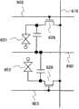
在使用发光元件的发光显示装置中,像素部中具有多个薄膜晶体管,并且在像素部中还具有将薄膜晶体管的栅电极和其他薄膜晶体管的源极布线或漏极布线连接在一起的区域。另外,在使用发光元件的发光显示装置的驱动电路中具有将薄膜晶体管的栅电极与该薄膜晶体管的源极布线或漏极布线连接在一起的区域。In a light-emitting display device using a light-emitting element, a pixel portion includes a plurality of thin film transistors and a region for connecting gate electrodes of the thin film transistors to source wiring or drain wiring of other thin film transistors. In addition, a driving circuit of a light-emitting display device using a light-emitting element has a region for connecting a gate electrode of a thin-film transistor to a source wiring or a drain wiring of the thin-film transistor.
因为薄膜晶体管容易被静电等损坏,所以优选相对于栅极线或源极线将用于保护像素部的薄膜晶体管的保护电路设置在同一衬底上。保护电路优选使用包含氧化物半导体层的非线性元件来形成。Since thin film transistors are easily damaged by static electricity or the like, it is preferable to provide a protection circuit for protecting the thin film transistors of the pixel portion on the same substrate as the gate line or the source line. The protection circuit is preferably formed using a nonlinear element including an oxide semiconductor layer.
注意,为了方便起见而在本说明书中附加第一、第二等序数词,但其并不表示工序顺序或叠层顺序。此外,本说明书中的序数词不表示限定发明的固有名称。Note that ordinal numerals such as first and second are added in this specification for the sake of convenience, but they do not indicate the order of steps or the order of lamination. In addition, the ordinal number in this specification does not represent the proper name which limits an invention.
本发明可以实现一种半导体装置,其中寄生电容被充分地降低并且具备即使沟道长度较短也具有稳定的电特性的薄膜晶体管。The present invention can realize a semiconductor device in which parasitic capacitance is sufficiently reduced and has a thin film transistor having stable electrical characteristics even if the channel length is short.
附图说明Description of drawings
图1A是示出本发明的一个方式的俯视图,图1B及1C是其剖视图;FIG. 1A is a plan view showing one mode of the present invention, and FIGS. 1B and 1C are cross-sectional views thereof;
图2A至2E是示出本发明的一个方式的工序剖视图;2A to 2E are process sectional views showing one embodiment of the present invention;
图3A和3B是示出本发明的一个方式的剖视图;3A and 3B are sectional views showing one mode of the present invention;
图4A1及4B1是示出本发明的一个方式的剖视图,图4A2及4B2是其俯视图;4A1 and 4B1 are cross-sectional views illustrating one mode of the present invention, and FIGS. 4A2 and 4B2 are top views thereof;
图5A及5C是示出本发明的一个方式的剖视图,图5B是其俯视图;5A and 5C are cross-sectional views illustrating an embodiment of the present invention, and FIG. 5B is a top view thereof;
图6A和6B是示出本发明的一个方式的剖视图;6A and 6B are sectional views showing one mode of the present invention;
图7A是示出本发明的一个方式的俯视图,图7B及7C是其剖视图;FIG. 7A is a plan view showing one mode of the present invention, and FIGS. 7B and 7C are cross-sectional views thereof;
图8A至8E是示出本发明的一个方式的工序剖视图;8A to 8E are process sectional views showing one embodiment of the present invention;
图9A和9B示出半导体装置;9A and 9B illustrate a semiconductor device;
图10A1、10A2和10B示出半导体装置;10A1, 10A2 and 10B illustrate semiconductor devices;
图11A和11B示出半导体装置;11A and 11B illustrate a semiconductor device;
图12示出半导体装置的像素等价电路;12 shows a pixel equivalent circuit of a semiconductor device;
图13A至13C示出半导体装置;13A to 13C illustrate a semiconductor device;
图14A和14B是半导体装置的方框图;14A and 14B are block diagrams of semiconductor devices;
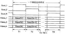
图15A示出信号线驱动电路的结构,图15B是示出其工作的时序图;Fig. 15A shows the structure of the signal line driving circuit, and Fig. 15B is a timing diagram showing its operation;
图16A至16D是示出移位寄存器的结构的电路图;16A to 16D are circuit diagrams showing the structure of a shift register;
图17A是示出移位寄存器的结构的电路图,图17B是示出其工作的时序图;Fig. 17A is a circuit diagram showing the structure of a shift register, and Fig. 17B is a timing diagram showing its operation;
图18示出半导体装置;Figure 18 shows a semiconductor device;
图19示出半导体装置;Figure 19 shows a semiconductor device;
图20是示出电子书阅读器的一个例子的外观图;FIG. 20 is an external view showing an example of an e-book reader;
图21A和21B是分别示出电视装置及数码相框的例子的外观图;21A and 21B are external views showing examples of a television set and a digital photo frame, respectively;
图22A和22B是示出游戏机的例子的外观图;22A and 22B are external views showing examples of gaming machines;
图23A和23B是分别示出便携式计算机及移动电话机的一个例子的外观图;23A and 23B are external views showing an example of a portable computer and a mobile phone, respectively;
图24示出半导体装置;Figure 24 shows a semiconductor device;
图25示出半导体装置;Figure 25 shows a semiconductor device;
图26示出半导体装置;Figure 26 shows a semiconductor device;
图27示出半导体装置;Figure 27 shows a semiconductor device;
图28示出半导体装置;Figure 28 shows a semiconductor device;
图29示出半导体装置;Figure 29 shows a semiconductor device;
图30示出半导体装置;Figure 30 shows a semiconductor device;
图31示出半导体装置;Figure 31 shows a semiconductor device;
图32示出半导体装置;Figure 32 shows a semiconductor device;
图33示出半导体装置;Figure 33 shows a semiconductor device;
图34示出半导体装置;Figure 34 shows a semiconductor device;
图35示出半导体装置;Figure 35 shows a semiconductor device;
图36A和36B示出半导体装置;36A and 36B illustrate a semiconductor device;
图37示出仿真所使用的氧化物半导体层的结构;FIG. 37 shows the structure of an oxide semiconductor layer used for simulation;
图38示出氧化物半导体层的氧密度的仿真结果;FIG. 38 shows simulation results of the oxygen density of the oxide semiconductor layer;
图39A至39C示出氧与氧化物半导体膜表面的相互作用。39A to 39C illustrate the interaction of oxygen with the surface of the oxide semiconductor film.
具体实施方式Detailed ways
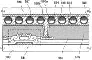
下面,关于本发明的实施方式将参照附图给予详细说明。注意,本发明并不局限于以下的说明,所属技术领域的普通技术人员可以很容易地理解本发明的方式和详细内容可以被变换为各种各样的形式。因此,本发明不应该被解释为仅限定在以下实施方式所记载的内容中。在以下说明的结构中,在不同附图中使用相同的附图标记来表示相同的部分或具有类似功能的部分,而省略重复说明。Hereinafter, embodiments of the present invention will be described in detail with reference to the drawings. Note that the present invention is not limited to the following description, and those skilled in the art can easily understand that the modes and details of the present invention can be changed into various forms. Therefore, the present invention should not be interpreted as being limited only to the contents described in the following embodiments. In the structures described below, the same reference numerals are used in different drawings to denote the same parts or parts having similar functions, and repeated descriptions are omitted.
实施方式1
在本实施方式中,参照图1A至1C、图2A至2E、图3A和3B以及图4A1、4A2、4B1和4B2对半导体装置及半导体装置的制造方法的一个方式进行说明。In this embodiment, one mode of a semiconductor device and a method of manufacturing the semiconductor device will be described with reference to FIGS. 1A to 1C , FIGS. 2A to 2E , FIGS. 3A and 3B , and FIGS.
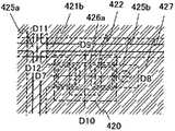
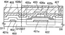
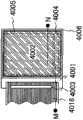
另外,图1A是配置在像素中的沟道保护型薄膜晶体管448的俯视图,图1B是沿着图1A的线D1-D2和D5-D6的剖视图。图1C是沿着图1A的线D3-D4的剖视图。此外,图2E与图1B相同。In addition, FIG. 1A is a top view of a channel protection
配置在像素中的薄膜晶体管448是沟道保护型(也称作沟道停止型)的薄膜晶体管,并且在具有绝缘表面的衬底400上包括:栅电极层421a、栅极绝缘层402、包括沟道形成区423的氧化物半导体层442、用作沟道保护层的氧化物绝缘层426a、源电极层425a以及漏电极层425b。另外,覆盖薄膜晶体管448并与氧化物绝缘层426a、源电极层425a及漏电极层425b相接触地设置有保护绝缘层403,且在其上层叠有平坦化绝缘层404。在平坦化绝缘层404上设置有与漏电极层425b接触的像素电极层427,并且像素电极层427电连接到薄膜晶体管448。The
像素用的薄膜晶体管448具有包括高电阻源区424a、高电阻漏区424b以及沟道形成区423的氧化物半导体层442。高电阻源区424a与源电极层425a的下面相接触而形成。高电阻漏区424b与漏电极层425b的下面相接触而形成。即使施加高电场,由于高电阻漏区或高电阻源区被用作缓冲区,因而可防止薄膜晶体管448被施加局部性的高电场,所以其耐压得到提高。The
配置在像素中的薄膜晶体管448的沟道形成区是氧化物半导体层442中所具有的与用作沟道保护层的氧化物绝缘层426a相接触并与栅电极层421a重叠的区域。由于薄膜晶体管448被氧化物绝缘层426a保护,从而可以防止氧化物半导体层442在形成源电极层425a、漏电极层425b的蚀刻工序中被蚀刻。The channel formation region of the
另外,为了实现具有高开口率的显示装置,采用具有透光性的导电膜来形成源电极层425a和漏电极层425b,从而形成薄膜晶体管448以作为具有透光性的薄膜晶体管。In addition, in order to realize a display device with a high aperture ratio, a light-transmitting conductive film is used to form the
另外,薄膜晶体管448的栅电极层421a采用具有透光性的导电膜来形成。In addition, the
在配置有薄膜晶体管448的像素中,使用对可见光具有透光性的导电膜来形成像素电极层427、电容电极层等其他的电极层或电容布线层等其他的布线层,以实现具有高开口率的显示装置。当然,栅极绝缘层402、氧化物绝缘层426a也优选使用对可见光具有透光性的膜来形成。In the pixel in which the
在本说明书中,对可见光具有透光性的膜是指其厚度对可见光的透过率为75%至100%的膜。当该膜具有导电性时也将其称为透明的导电膜。另外,也可以使用对可见光半透明的导电膜作为用作栅电极层、源电极层、漏电极层、像素电极层、其他的电极层和布线层的金属氧化物。对可见光半透明的导电膜是指其对可见光的透过率为50%至75%的膜。In this specification, a film having light transmittance to visible light means a film whose thickness has a transmittance to visible light of 75% to 100%. When the film is electrically conductive, it is also referred to as a transparent conductive film. In addition, a conductive film semitransparent to visible light can also be used as a metal oxide used as a gate electrode layer, a source electrode layer, a drain electrode layer, a pixel electrode layer, other electrode layers, and a wiring layer. The conductive film translucent to visible light refers to a film whose transmittance to visible light is 50% to 75%.
为了降低寄生电容,在栅极布线和源极布线交叉的布线交叉部中,在栅电极层421b和源电极层425a之间设置有栅极绝缘层402和氧化物绝缘层426b。另外,虽然使用不同的符号表示与沟道形成区423重叠的氧化物绝缘层426a和不与沟道形成区423重叠的氧化物半导体层426b,但是426a和426b是使用相同的材料在相同的工序中形成的层。In order to reduce parasitic capacitance, a
下面,参照图2A至2E对在同一衬底上制造薄膜晶体管448和布线交叉部的工序进行说明。不仅可以形成像素部的薄膜晶体管还可以形成驱动电路的薄膜晶体管。并且上述薄膜晶体管可以使用相同工序在同一衬底上制造。Next, the process of manufacturing the
首先,在具有绝缘表面的衬底400上形成具有透光性的导电膜之后,利用第一光刻工序形成栅电极层421a、421b。在像素部中,使用与栅电极层421a、421b相同的具有透光性的材料并利用同一第一光刻工序形成电容布线层。此外,当除了形成像素部还形成驱动电路时,在驱动电路需要电容时在驱动电路中也形成电容布线层。另外,还可以使用喷墨法来形成抗蚀剂掩模。当使用喷墨法形成抗蚀剂掩模时不需要光掩模,由此可以降低制造成本。First, after a light-transmitting conductive film is formed on a
对于能够用作具有绝缘表面的衬底400的衬底没有太大的限制,只要其至少需要具有能够耐受后面的加热处理的耐热性。可以使用玻璃衬底作为具有绝缘表面的衬底400。There is not much limitation on the substrate that can be used as the
另外,当后面的加热处理的温度较高时,优选使用应变点为730℃以上的玻璃衬底。另外,作为玻璃衬底,例如可以使用如铝硅酸盐玻璃、铝硼硅酸盐玻璃或钡硼硅酸盐玻璃等的玻璃材料。另外,通过使玻璃衬底相比氧化硼而含有更多的氧化钡(BaO),可以获得更实用的耐热玻璃。因此,优选使用相比B2O3包含更多的BaO的玻璃衬底。In addition, when the temperature of the subsequent heat treatment is high, it is preferable to use a glass substrate having a strain point of 730° C. or higher. In addition, as the glass substrate, for example, a glass material such as aluminosilicate glass, aluminoborosilicate glass, or barium borosilicate glass can be used. In addition, more practical heat-resistant glass can be obtained by making the glass substrate contain more barium oxide (BaO) than boron oxide. Therefore, it is preferable to use a glass substrate containing more BaO than B2 O3 .
另外,还可以使用如陶瓷衬底、石英衬底、蓝宝石衬底等的由绝缘体构成的衬底代替上述玻璃衬底。此外,还可以使用晶化玻璃等。In addition, a substrate made of an insulator such as a ceramic substrate, a quartz substrate, a sapphire substrate, or the like may also be used instead of the above-mentioned glass substrate. In addition, crystallized glass and the like can also be used.
另外,还可以将用作基底膜的绝缘膜设置在衬底400与栅电极层421a、421b之间。基底膜具有防止杂质元素从衬底400扩散的作用,可以由选自氮化硅膜、氧化硅膜、氮氧化硅膜、和氧氮化硅膜中的一种的单层或多种膜的叠层结构来形成。In addition, an insulating film serving as a base film may also be provided between the
栅电极层421a、421b的材料可以采用对可见光具有透光性的导电材料,例如可采用以下任意一种金属氧化物:In-Sn-Zn-O类、In-Al-Zn-O类、Sn-Ga-Zn-O类、Al-Ga-Zn-O类、Sn-Al-Zn-O类、In-Zn-O类、Sn-Zn-O类、Al-Zn-O类、In-O类、Sn-O类、Zn-O类的金属氧化物。并可以在大于等于50nm至小于等于300nm的范围内适当地选择其厚度。作为用作栅电极层421a、421b的金属氧化物的成膜方法,可以使用溅射法、真空蒸镀法(电子束蒸镀法等)、电弧放电离子电镀法或喷涂法。当使用溅射法时,优选使用含有大于等于2wt%且小于等于10wt%的SiO2的靶进行成膜,以使具有透光性的导电膜含有阻碍晶化的SiOx(X>0)。这样,优选防止在后面的工序中进行用于脱水化或脱氢化的加热处理时具有透光性的导电膜被晶化。The material of the
氧化物半导体优选是含有In的氧化物半导体,更优选是含有In及Ga的氧化物半导体。为了获得i型(本征)氧化物半导体层,包括脱水化或脱氢化的工序是有效的。The oxide semiconductor is preferably an oxide semiconductor containing In, more preferably an oxide semiconductor containing In and Ga. In order to obtain an i-type (intrinsic) oxide semiconductor layer, a process including dehydration or dehydrogenation is effective.
接着,在栅电极层421a、421b上形成栅极绝缘层402。Next, the
通过利用等离子体CVD法或溅射法等并使用氧化硅层、氮化硅层、氧氮化硅层、氮氧化硅层或氧化铝层的单层或叠层,可以形成栅极绝缘层402。例如,可使用SiH4、氧及氮以作为成膜气体并通过等离子体CVD法来形成氧氮化硅层。栅极绝缘层402具有大于等于100nm且小于等于500nm的厚度。当采用叠层结构时,形成厚度大于等于50nm且小于等于200nm的第一栅极绝缘层,并在第一栅极绝缘层上层叠厚度大于等于5nm且小于等于300nm的第二栅极绝缘层。The
在本实施方式中,通过等离子体CVD法形成厚度小于等于200nm的氮化硅层作为栅极绝缘层402。In this embodiment, a silicon nitride layer with a thickness of 200 nm or less is formed as the
接着,在栅极绝缘层402上形成厚度大于等于2nm且小于等于200nm的氧化物半导体膜430(参照图2A)。为了即使在形成氧化物半导体膜之后进行用于脱水化或脱氢化的加热处理时也使氧化物半导体膜处于非晶状态,优选将氧化物半导体膜430的厚度设定为小于等于50nm。通过将氧化物半导体膜的厚度形成得薄,在形成膜之后进行加热处理时可以抑制氧化物半导体层晶化。Next, an
氧化物半导体膜430使用In-Ga-Zn-O类非单晶膜、In-Sn-Zn-O类、In-Al-Zn-O类、Sn-Ga-Zn-O类、Al-Ga-Zn-O类、Sn-Al-Zn-O类、In-Zn-O类、Sn-Zn-O类、Al-Zn-O类、In-O类、Sn-O类、Zn-O类的氧化物半导体膜来形成。在本实施方式中,使用In-Ga-Zn-O类氧化物半导体靶并通过溅射法来形成氧化物半导体膜430。另外,可以在稀有气体(典型是氩)气氛下、在氧气氛下或者在稀有气体(典型是氩)及氧的气氛下通过溅射法来形成氧化物半导体膜430。当使用溅射法时,使用含有大于等于2wt%且小于等于10wt%的SiO2的靶来进行成膜,而使氧化物半导体膜430含有阻碍晶化的SiOx(X>0)。这样,优选防止在后面的工序中进行用于脱水化或脱氢化的加热处理时氧化物半导体膜430被晶化。The
在此,在氩及氧(氩∶氧=30sccm∶20sccm 氧流量比率40%)的气氛下,使用包含In、Ga及Zn的氧化物半导体靶(In2O3∶Ga2O3∶ZnO=1∶1∶1[摩尔比])并以如下条件形成氧化物半导体膜,该条件是:衬底和靶之间的距离是100mm;压力是0.2Pa;直流(DC)电源是0.5kW。另外,当使用脉冲直流(DC)电源时,由于可以减少尘屑且膜厚度分布也均匀,所以是优选的。将In-Ga-Zn-O类非单晶膜的厚度形成为5nm至200nm。在本实施方式中,使用In-Ga-Zn-O类氧化物半导体靶并通过溅射法来形成20nm厚的In-Ga-Zn-O类非单晶膜作为氧化物半导体膜。Here, in an atmosphere of argon and oxygen (argon: oxygen = 30sccm: 20sccm
作为溅射法,有作为溅射电源使用高频电源的RF溅射法、DC溅射法、以及以脉冲方式施加偏压的脉冲DC溅射法。RF溅射法主要用于绝缘膜的形成,而DC溅射法主要用于金属膜的形成。As the sputtering method, there are RF sputtering method using a high-frequency power source as a sputtering power source, DC sputtering method, and pulsed DC sputtering method applying a bias voltage in a pulsed manner. The RF sputtering method is mainly used for the formation of an insulating film, and the DC sputtering method is mainly used for the formation of a metal film.
此外,还有可以设置多个材料不同的靶的多源溅射装置。多源溅射装置中,既可以在同一处理室中层叠形成不同材料的膜,又可以在同一处理室中使多种材料同时进行放电来形成多种材料的膜。In addition, there is a multi-source sputtering device that can set a plurality of targets of different materials. In the multi-source sputtering apparatus, films of different materials can be laminated and formed in the same processing chamber, and films of multiple materials can be formed by discharging multiple materials simultaneously in the same processing chamber.
此外,有在处理室内具备磁体机构并用于磁控管溅射法的溅射装置;以及用于不使用辉光放电而利用使用微波来产生的等离子体的ECR溅射法的溅射装置。In addition, there are sputtering apparatuses used in the magnetron sputtering method provided with a magnet mechanism in the processing chamber, and sputtering apparatuses used in the ECR sputtering method using plasma generated using microwaves without using glow discharge.
此外,作为使用溅射法的成膜方法,还有:在成膜时使靶物质与溅射气体成分产生化学反应而形成它们的化合物薄膜的反应溅射法;以及在成膜时对衬底也施加电压的偏压溅射法。In addition, as a film-forming method using the sputtering method, there are: a reactive sputtering method in which a target substance and a sputtering gas component are chemically reacted to form a thin film of their compound during film formation; A bias sputtering method in which a voltage is also applied.
接着,通过第二光刻工序将氧化物半导体膜430加工为岛状氧化物半导体层。也可以通过喷墨法形成用于形成岛状氧化物半导体层的抗蚀剂掩模。当通过喷墨法形成抗蚀剂掩模时不需要光掩模,因此可以降低制造成本。Next, the
接着,对氧化物半导体层进行脱水化或脱氢化。将进行脱水化或脱氢化的第一加热处理的温度设定为大于等于400℃且低于衬底的应变点,优选设定为大于等于425℃。注意,当加热处理的温度大于等于425℃时加热处理时间可小于等于1小时,但是当加热处理的温度低于425℃时加热处理时间被设定为长于1小时。在此,将衬底放入到加热处理装置之一的电炉中,在氮气氛下对氧化物半导体层进行加热处理,然后不使其暴露于大气而防止水或氢再次混入到氧化物半导体层,从而获得氧化物半导体层。在本实施方式中,在温度从进行氧化物半导体层的脱水化或脱氢化所需的加热温度T下降到足以防止水再次混入的温度为止,一直使用一个用于热处理的炉。具体而言,在直到温度变得比加热温度T要低100℃或更多为止,在氮气氛下进行缓冷。另外,不局限于氮气氛,而在氦、氖、氩等稀有气体气氛下进行脱水化或脱氢化。Next, the oxide semiconductor layer is dehydrated or dehydrogenated. The temperature of the first heat treatment for dehydration or dehydrogenation is set to 400°C or higher and lower than the strain point of the substrate, preferably 425°C or higher. Note that the heat treatment time may be 1 hour or less when the heat treatment temperature is 425° C. or higher, but the heat treatment time is set to be longer than 1 hour when the heat treatment temperature is lower than 425° C. Here, the substrate is placed in an electric furnace which is one of the heat treatment apparatuses, the oxide semiconductor layer is heat-treated in a nitrogen atmosphere, and then the oxide semiconductor layer is not exposed to the atmosphere to prevent water or hydrogen from being mixed into the oxide semiconductor layer again. , thereby obtaining an oxide semiconductor layer. In the present embodiment, one furnace for heat treatment is used until the temperature drops from the heating temperature T required for dehydration or dehydrogenation of the oxide semiconductor layer to a temperature sufficient to prevent water from re-mingling. Specifically, slow cooling is performed in a nitrogen atmosphere until the temperature becomes lower than the heating temperature T by 100° C. or more. In addition, dehydration or dehydrogenation is performed not only in a nitrogen atmosphere, but also in a rare gas atmosphere such as helium, neon, or argon.
另外,在第一加热处理中,优选氮或氦、氖、氩等稀有气体不包含水、氢等。另外,优选将导入于加热处理装置中的氮或氦、氖、氩等稀有气体的纯度设定为大于等于6N(99.9999%),优选设定为大于等于7N(99.99999%)(即,将杂质浓度设定为小于等于1ppm,优选设定小于等于0.1ppm)。In addition, in the first heat treatment, it is preferable that nitrogen or rare gases such as helium, neon, and argon do not contain water, hydrogen, or the like. In addition, it is preferable to set the purity of nitrogen or rare gases such as helium, neon, and argon introduced into the heat treatment device to be equal to or greater than 6N (99.9999%), preferably equal to or greater than 7N (99.99999%) (that is, the impurities The concentration is set to be equal to or less than 1 ppm, preferably set to be equal to or less than 0.1 ppm).
另外,根据第一加热处理的条件或氧化物半导体层的材料,有时使氧化物半导体层进行晶化,以成为微晶膜或多晶膜。In addition, depending on the conditions of the first heat treatment or the material of the oxide semiconductor layer, the oxide semiconductor layer may be crystallized to form a microcrystalline film or a polycrystalline film.
另外,也可以对加工成岛状氧化物半导体层之前的氧化物半导体膜430进行第一加热处理。在此情况下,在第一加热处理之后从加热装置拿出衬底,以进行光刻工序。In addition, the first heat treatment may be performed on the
另外,也可以在形成氧化物半导体膜430之前在惰性气体气氛(氮或氦、氖、氩等)下或者在氧气氛下进行加热处理(大于等于400℃且低于衬底的应变点),而去除包含在栅极绝缘层内的氢及水等杂质。In addition, heat treatment (400° C. or higher and lower than the strain point of the substrate) may be performed under an inert gas atmosphere (nitrogen or helium, neon, argon, etc.) or an oxygen atmosphere before forming the
接着,在栅极绝缘层402及氧化物半导体层上形成氧化物绝缘膜之后,通过第三光刻工序形成抗蚀剂掩模,选择性地进行蚀刻来形成氧化物绝缘层426a、426b,然后去除抗蚀剂掩模。在该阶段,氧化物半导体层中形成有与氧化物绝缘层接触的区域,并且该区域中,隔着栅极绝缘层与栅电极层重叠且与氧化物绝缘层426a重叠的区域成为沟道形成区。另外,也形成有与覆盖氧化物半导体层的边缘及侧面的氧化物绝缘层426b重叠的区域。Next, after forming an oxide insulating film on the
将氧化物绝缘膜的厚度至少设定为大于等于1nm,并且可以适当地使用溅射法等防止水、氢等杂质混入到氧化物绝缘膜的方法来形成氧化物绝缘膜。在本实施方式中,使用溅射法形成300nm厚的氧化硅膜作为氧化物绝缘膜。可将形成膜时的衬底温度设定为大于等于室温且小于等于300℃,在本实施方式中将该衬底温度设定为室温。可以在稀有气体(典型为氩)气氛下、在氧气氛下或者在稀有气体(典型为氩)和氧的气氛下通过溅射法形成氧化硅膜。作为靶,可以使用氧化硅靶或硅靶。例如,可以使用硅靶在氧及氮气氛下通过溅射法形成氧化硅膜。作为与被低电阻化的氧化物半导体层相接触地形成的氧化物绝缘膜,使用不包含水分、氢离子、OH-等杂质且阻挡上述杂质从外部侵入的无机绝缘膜。典型地使用氧化硅膜、氮氧化硅膜、氧化铝膜或者氧氮化铝膜等。The thickness of the oxide insulating film is set to at least 1 nm, and the oxide insulating film can be formed by appropriately using a method such as sputtering to prevent impurities such as water and hydrogen from being mixed into the oxide insulating film. In this embodiment mode, a silicon oxide film having a thickness of 300 nm is formed as an oxide insulating film by using a sputtering method. The substrate temperature at the time of film formation can be set to be equal to or higher than room temperature and equal to or lower than 300° C., and the substrate temperature is set to room temperature in this embodiment mode. The silicon oxide film can be formed by sputtering under a rare gas (typically argon) atmosphere, under an oxygen atmosphere, or under a rare gas (typically argon) and oxygen atmosphere. As the target, a silicon oxide target or a silicon target can be used. For example, a silicon oxide film can be formed by sputtering in an oxygen and nitrogen atmosphere using a silicon target. As the oxide insulating film formed in contact with the low-resistance oxide semiconductor layer, an inorganic insulating film that does not contain impurities such as water, hydrogen ions, and OH− and blocks the entry of these impurities from the outside is used. Typically, a silicon oxide film, a silicon oxynitride film, an aluminum oxide film, an aluminum oxynitride film, or the like is used.
接着,在惰性气体气氛下或氮气体气氛下进行第二加热处理(优选是大于等于200℃且小于等于400℃,例如大于等于250℃且小于等于350℃)(参照图2B)。例如,在氮气氛下进行250℃且1小时的第二加热处理。当进行第二加热处理时,氧化物半导体层442与氧化物绝缘层局部重叠的状态下对氧化物半导体层442进行加热。氧化物半导体层442中的接触部分是与氧化物绝缘层426b重叠的端部及与氧化物绝缘层426a重叠的部分。另外,当进行第二加热处理时,不与氧化物绝缘层重叠的氧化物半导体层442的一部分在露出的状态下被加热。当在氧化物半导体层442露出的状态下且在氮或惰性气体气氛下进行加热处理时,可以使氧化物半导体层422中露出且高电阻(i型)的区域低电阻化。氧化物绝缘层426a以与氧化物半导体层442的沟道形成区相接触的方式在该沟道形成区上形成,并用作沟道保护层。Next, a second heat treatment (preferably greater than or equal to 200°C and less than or equal to 400°C, for example, greater than or equal to 250°C and less than or equal to 350°C) is performed under an inert gas atmosphere or a nitrogen gas atmosphere (see FIG. 2B ). For example, the second heat treatment is performed at 250° C. for 1 hour in a nitrogen atmosphere. When the second heat treatment is performed, the
接着,在栅极绝缘层402、氧化物绝缘层426a、426b以及氧化物半导体层442上形成具有透光性的导电膜。然后通过第四光刻工序形成抗蚀剂掩模,选择性地进行蚀刻来形成源电极层425a及漏电极层425b(参照图2C)。具有透光性的导电膜通过使用溅射法、真空蒸镀法(电子束蒸镀法等)、电弧放电离子电镀法、喷射法来形成。作为导电膜的材料,可以使用对可见光具有透光性的导电材料,例如可使用以下金属氧化物:In-Sn-Zn-O类、In-Al-Zn-O类、Sn-Ga-Zn-O类、Al-Ga-Zn-O类、Sn-Al-Zn-O类、In-Zn-O类、Sn-Zn-O类、Al-Zn-O类、In-O类、Sn-O类、Zn-O类的金属氧化物。并且在大于等于50nm且小于等于300nm的范围内适当地选择导电膜的厚度。当使用溅射法时,优选使用包含大于等于2wt%且小于等于10wt%的SiO2的靶来进行成膜,使具有透光性的导电膜包含阻碍晶化的SiOx(X>0)。这样,优选防止在后面的工序中进行加热处理时具有透光性的导电膜被晶化。Next, a light-transmitting conductive film is formed on the
另外,也可以通过喷墨法形成用来形成源电极层425a、漏电极层425b的抗蚀剂掩模。当通过喷墨法形成抗蚀剂掩模时不需要光掩模,因此可以缩减制造成本。In addition, a resist mask for forming the
接着,在氧化物绝缘层426a、426b、源电极层425a、漏电极层425b上形成保护绝缘层403。在本实施方式中,使用RF溅射法形成氮化硅膜。因为RF溅射法的量产性好,所以作为保护绝缘层403的形成方法优选采用RF溅射法。保护绝缘层403使用不包含水分、氢离子、OH-等杂质且阻挡上述杂质从外部侵入的无机绝缘膜来形成。典型地使用氮化硅膜、氮化铝膜、氮氧化硅膜或者氧氮化铝膜等。当然,保护绝缘层403是具有透光性的绝缘膜。Next, the protective insulating
接着,在保护绝缘层403上形成平坦化绝缘层404。作为平坦化绝缘层404,可以使用具有耐热性的有机材料如聚酰亚胺、丙烯酸树脂、苯并环丁烯、聚酰胺、环氧树脂等。另外,除了上述有机材料之外,还可以使用低介电常数材料(low-k材料)、硅氧烷类树脂、PSG(磷硅玻璃)、BPSG(硼磷硅玻璃)等。也可以通过层叠多个由这些材料形成的绝缘膜来形成平坦化绝缘层404。Next, a
另外,硅氧烷类树脂相当于以硅氧烷类材料为起始材料而形成的包含Si-O-Si键的树脂。硅氧烷类树脂也可以包括有机基(例如烷基、芳基)、氟基团以作为取代基。另外,有机基也可以具有氟基团。In addition, the siloxane-based resin corresponds to a resin containing a Si-O-Si bond formed from a siloxane-based material as a starting material. The siloxane-based resin may also contain organic groups (eg, alkyl groups, aryl groups), fluorine groups as substituents. In addition, the organic group may have a fluorine group.
对平坦化绝缘层404的形成方法没有特别的限制,可以根据其材料采用如下方法:溅射法、SOG法、旋涂法、浸渍法、喷涂法、液滴喷射法(喷墨法、丝网印刷、胶版印刷等)等。而且平坦化绝缘层404可通过刮片、辊涂机、幕涂机、刮刀涂布机等来形成。The formation method of the
接着,进行第五光刻工序,形成抗蚀剂掩模,通过对平坦化绝缘层404及保护绝缘层403进行蚀刻来形成到达漏电极层425b的接触孔441。然后去除抗蚀剂掩模(参照图2D)。如图2D所示,在接触孔的下方设置有氧化物绝缘层426b,与在接触孔的下方没有设置氧化物绝缘层的情况相比可以将要去除的平坦化绝缘层的厚度设定得薄,而可以缩短蚀刻时间。另外,与在接触孔的下方没有设置氧化物绝缘层的情况相比可以将接触孔441的深度设定得浅,而可以使在与接触孔441重叠的区域中在后面的工序中形成的具有透光性的导电膜的覆盖性良好。另外,通过这里的蚀刻还形成到达栅电极层421b的接触孔。另外,也可以通过喷墨法形成用来形成到达漏电极层425b的接触孔的抗蚀剂掩模。当通过喷墨法形成抗蚀剂掩模时不需要光掩模,因此可以缩减制造成本。Next, a fifth photolithography step is performed to form a resist mask, and by etching the
接着,形成具有透光性的导电膜。通过溅射法或真空蒸镀法等并使用氧化铟(In2O3)、氧化铟氧化锡合金(In2O3-SnO2,简称为ITO)等来形成具有透光性的导电膜。作为具有透光性的导电膜的其他材料,可以使用含有氮的Al-Zn-O类非单晶膜,即Al-Zn-O-N类非单晶膜、Zn-O-N类非单晶膜、或Sn-Zn-O-N类非单晶膜。另外,Al-Zn-O-N类非单晶膜的锌的组成比(原子百分比)小于等于47原子%,该锌的组成比大于非单晶膜中的铝的组成比(原子百分比),并且非单晶膜中的铝的组成比(原子百分比)大于非单晶膜中的氮的组成比(原子百分比)。上述材料使用盐酸类的溶液进行蚀刻。但是,由于对ITO的蚀刻特别容易产生残渣,因此也可以使用氧化铟氧化锌合金(In2O3-ZnO),以便改善蚀刻加工性。Next, a light-transmitting conductive film is formed. A light-transmitting conductive film is formed using indium oxide (In2 O3 ), indium oxide tin oxide alloy (In2 O3 -SnO2 , abbreviated as ITO) or the like by sputtering or vacuum deposition. As another material of the conductive film having light transmission, an Al-Zn-O non-single-crystal film containing nitrogen, that is, an Al-Zn-ON non-single-crystal film, a Zn-ON non-single-crystal film, or Sn-Zn-ON non-single crystal film. In addition, the composition ratio (atomic percentage) of zinc in the Al-Zn-ON non-single crystal film is 47 atomic % or less, the composition ratio of zinc is larger than the composition ratio (atomic percentage) of aluminum in the non-single crystal film, and is not The composition ratio (atomic percentage) of aluminum in the single crystal film is larger than the compositional ratio (atomic percentage) of nitrogen in the non-single crystal film. The above materials are etched using a solution of hydrochloric acid. However, since etching of ITO is particularly prone to residues, an indium oxide zinc oxide alloy (In2 O3 —ZnO) may also be used in order to improve etching workability.
另外,具有透光性的导电膜的组成比的单位为原子百分比,并且通过使用电子探针显微分析仪(EPMA:Electron Probe X-ray MicroAnalyzer)的分析进行评价。In addition, the unit of the composition ratio of the light-transmitting conductive film is an atomic percent, and it evaluates by the analysis using an electron probe microanalyzer (EPMA: Electron Probe X-ray MicroAnalyzer).
接着,进行第六光刻工序,形成抗蚀剂掩模,通过蚀刻去除不需要的部分来形成像素电极层427,然后去除抗蚀剂掩模(参照图2E)。Next, a sixth photolithography process is performed to form a resist mask, remove unnecessary portions by etching to form a
通过上述工序使用六个掩模可以在同一衬底上形成薄膜晶体管448和寄生电容降低的布线交叉部。设置于像素的薄膜晶体管448是包括氧化物半导体层442的沟道保护型薄膜晶体管,该氧化物半导体层442包括高电阻源区424a、高电阻漏区424b及沟道形成区423。因此,即使施加高电场,由于高电阻漏区424b或高电阻源区424a用作缓冲区域,因而可防止薄膜晶体管448被施加局部性的高电场,可提高耐压。The
另外,也可以在同一衬底上形成以栅极绝缘层402为电介质且由电容布线层和电容电极形成的存储电容器。通过对应于像素以矩阵状配置的像素部的每个像素来配置薄膜晶体管448和存储电容器,可以获得用来制造有源矩阵型显示装置的一个衬底。在本说明书中,为了方便起见将这种衬底称为有源矩阵型衬底。In addition, a storage capacitor that uses the
另外,也可以在同一衬底上设置驱动电路的薄膜晶体管。通过在同一衬底上形成驱动电路和像素部,可以缩短驱动电路与传输外部信号的电路之间的连接布线,从而可以实现半导体装置的小型化、低成本化。In addition, the thin film transistors of the driver circuit may be provided on the same substrate. By forming the driver circuit and the pixel portion on the same substrate, the connection wiring between the driver circuit and the circuit for transmitting external signals can be shortened, and the size and cost of the semiconductor device can be reduced.
另外,图1B所示的用于像素的薄膜晶体管448中,氧化物半导体层442的边缘部具有与氧化物绝缘层426b重叠的第一区域424c、第二区域424d。作为氧化物半导体层442的边缘部的第一区域424c、第二区域424d处于与沟道形成区423相同的氧过剩状态。因此当氧化物半导体层和与氧化物半导体层的电位不同的布线配置得彼此靠近时可以实现漏电流的降低和寄生电容的降低。In addition, in the
特别是在驱动电路中,为了实现高集成化,优选缩小多个布线和多个氧化物半导体层的间隔地进行配置。在这种驱动电路中,通过与氧化物绝缘层426b重叠地设置第一区域424c及第二区域424d来进行漏电流的降低或寄生电容的降低是有效的。另外,当串联或并联配置多个薄膜晶体管时,通过将多个薄膜晶体管中的氧化物半导体层形成为一个岛状物,并使氧化物半导体层与氧化物绝缘层426b重叠,从而进行各个元件的分离。这样,与氧化物绝缘层426b重叠的区域成为元件分离区域。通过上述方法,可以在窄面积中配置多个薄膜晶体管,从而可以实现驱动电路的高度集成化。In particular, in a driver circuit, in order to realize high integration, it is preferable to arrange a plurality of wirings and a plurality of oxide semiconductor layers so that the intervals between them are reduced. In such a drive circuit, it is effective to reduce leakage current or parasitic capacitance by providing the
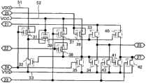
实施方式2
在本实施方式中示出使用实施方式1所示的薄膜晶体管在同一衬底上形成像素部和驱动电路来制造有源矩阵型液晶显示装置的一个例子。This embodiment mode shows an example in which an active matrix liquid crystal display device is manufactured by forming a pixel portion and a driver circuit over the same substrate using the thin film transistor described in
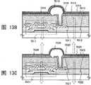
图3A示出有源矩阵衬底的截面结构的一个例子。FIG. 3A shows an example of a cross-sectional structure of an active matrix substrate.
在实施方式1中说明了像素部的薄膜晶体管及布线交叉部,而在本实施方式中除了薄膜晶体管、布线交叉部以外还对驱动电路部的薄膜晶体管、存储电容器、栅极布线、源极布线的端子部进行说明。电容器、栅极布线、源极布线的端子部可以通过与实施方式1所示的制造工序相同的工序形成。另外,在像素部的用作显示区域的部分中,栅极布线、源极布线及电容布线层都由具有透光性的导电膜形成,且具有高开口率。In
在图3A中,与像素电极层227电连接的薄膜晶体管220是设置在像素部中的沟道保护型薄膜晶体管。而在本实施方式中使用具有与实施方式1的薄膜晶体管448相同的结构的晶体管。另外,薄膜晶体管220的栅电极层的在沟道长度方向上的宽度小于薄膜晶体管220的氧化物半导体层的在沟道长度方向上的宽度。In FIG. 3A , the
利用与薄膜晶体管220的栅电极层相同的具有透光性的材料和相同工序形成的电容布线层230隔着用作电介质的栅极绝缘层202与电容电极231重叠,以形成存储电容器。另外,电容电极231利用与薄膜晶体管220的源电极层或漏电极层相同的具有透光性的材料和相同工序形成。因此,因为薄膜晶体管220具有透光性且每个存储电容器也具有透光性,所以可以提高开口率。
从提高开口率的观点而言,存储电容器具有透光性是重要的。尤其是因为在10英寸以下的小型液晶显示面板中通过增加栅极布线的数量等来实现显示图像的高清晰化,所以即使像素尺寸减小也可以实现高开口率。另外,由于薄膜晶体管220及存储电容器的结构部件通过使用具有透光性的膜来实现广视角,因此即使将一个像素分割为多个子像素也可以实现高开口率。即,即使配置高密度的薄膜晶体管也可以确保大开口率,从而可以确保充分的显示区域的面积。例如,当在一个像素内具有2至4个子像素及存储电容器时,因为薄膜晶体管具有透光性且各存储电容器也具有透光性,所以可以提高开口率。From the viewpoint of increasing the aperture ratio, it is important for the storage capacitor to have light transmittance. In particular, in a small liquid crystal display panel of 10 inches or less, the number of gate wirings is increased to achieve higher definition of the displayed image, so even if the pixel size is reduced, a high aperture ratio can be realized. In addition, since the thin-
另外,存储电容器设置在像素电极层227的下方,并且存储电极231电连接到像素电极层227。In addition, a storage capacitor is disposed under the
虽然在本实施方式中示出使用电容电极231及电容布线层230来形成存储电容器的例子,但是对存储电容器的结构没有特别的限制。例如,也可以不设置电容布线层而使像素电极层隔着平坦化绝缘层、保护绝缘层及栅极绝缘层与相邻像素的栅极布线重叠,以形成存储电容器。In this embodiment mode, an example is shown in which a storage capacitor is formed using the
另外,在图3A中,为了形成大电容,存储电容器仅包括在电容布线层和电容电极之间的栅极绝缘层202,为了降低寄生电容,布线交叉部包括设置在栅电极层421b和栅电极层421b的上方形成的布线之间的栅极绝缘层202和氧化物绝缘层266b。在存储电容器中,为了在电容布线层和电容电极之间仅设置有栅极绝缘层202,选择蚀刻条件或栅极绝缘层的材料,使得用于去除氧化物绝缘层266b的蚀刻可允许只留下栅极绝缘层202。在本实施方式中,因为氧化物绝缘层266b是通过溅射法得到的氧化硅膜且栅极绝缘层202是通过等离子体CVD法得到的氮化硅膜,所以可以实现选择性的去除。另外,当使用了会使得氧化物绝缘层266b和栅极绝缘层202以相同蚀刻条件去除的材料时,优选将厚度设定成即使一部分栅极绝缘层的厚度减小也至少使一部分栅极绝缘层残留而可以形成电容。为了将存储电容器形成得大,优选将栅极绝缘层的厚度设定得薄,所以也可为,当进行用于去除氧化物绝缘层266b的蚀刻时使电容布线上的一部分栅极绝缘层的厚度减小。In addition, in FIG. 3A, in order to form a large capacitance, the storage capacitor only includes the
另外,薄膜晶体管260是设置在驱动电路中的沟道保护型的薄膜晶体管。薄膜晶体管260的沟道长度L比薄膜晶体管220短,以实现工作速度的高速化。优选将设置在驱动电路中的沟道保护型薄膜晶体管的沟道长度L设定为大于等于0.1μm且小于等于2μm。薄膜晶体管260的栅电极层261的在沟道长度方向上的宽度大于薄膜晶体管260的氧化物半导体层的在沟道长度方向上的宽度。并且栅电极层261的端面隔着栅极绝缘层202及氧化物绝缘层266b与源电极层265a或漏电极层265b重叠。In addition, the
薄膜晶体管260在具有绝缘表面的衬底200上包括栅电极层261、栅极绝缘层202、氧化物半导体层、源电极层265a及漏电极层265b,该氧化物半导体层至少具有沟道形成区263、高电阻源区264a及高电阻漏区264b。另外,设置有与沟道形成区263接触的氧化物绝缘层266a。The
驱动电路的薄膜晶体管260的栅电极层也可以与设置在氧化物半导体层上方的导电层267电连接。此时,使用与用于对薄膜晶体管220的漏电极层和像素电极层227进行电连接的接触孔相同的光掩模,对平坦化绝缘层204、保护绝缘层203、氧化物绝缘层266b、栅极绝缘层202选择性地进行蚀刻来形成接触孔。通过该接触孔使导电层267与驱动电路的薄膜晶体管260的栅电极层261电连接。The gate electrode layer of the
保护绝缘层203使用氮化硅膜、氮化铝膜、氮氧化硅膜、氧氮化铝膜等无机绝缘膜。在本实施方式中使用氮化硅膜。An inorganic insulating film such as a silicon nitride film, an aluminum nitride film, a silicon oxynitride film, or an aluminum oxynitride film is used for the protective insulating
另外,薄膜晶体管260中,栅电极层261的宽度大于氧化物半导体层的宽度。另外,氧化物绝缘层266b与氧化物半导体层的边缘部重叠并与栅电极层261重叠。氧化物绝缘层266b起到如下功能:增加漏电极层265b和栅电极层261的间隔来降低形成在漏电极层265b和栅电极层261之间的寄生电容。与氧化物绝缘层266b重叠的氧化物半导体层的第一区域264c、第二区域264d处于与沟道形成区域263相同的氧过剩状态,并降低漏电流和寄生电容。In addition, in the
另外,当液晶显示面板的尺寸超过10英寸例如为60英寸、120英寸时,具有透光性的布线的布线电阻有可能成为难题,因此优选布线的一部分采用金属布线来降低布线电阻。例如,源电极层265a及漏电极层265b采用Ti等的金属布线来形成。因为形成金属布线,所以与实施方式1相比掩模的数目增加一个。In addition, when the size of the liquid crystal display panel exceeds 10 inches, such as 60 inches or 120 inches, the wiring resistance of the light-transmitting wiring may become a problem. Therefore, it is preferable to use metal wiring for part of the wiring to reduce the wiring resistance. For example, the
此时,在被脱水化或脱氢化的氧化物半导体层上与其相接触地形成由Ti等金属电极构成的源电极层或漏电极层,形成与源电极层重叠的高电阻源区和与漏电极层重叠的高电阻漏区,并且高电阻源区和高电阻漏区之间的区域用作沟道形成区。At this time, a source electrode layer or a drain electrode layer made of a metal electrode such as Ti is formed in contact with the dehydrated or dehydrogenated oxide semiconductor layer, and a high-resistance source region and a drain electrode layer overlapping the source electrode layer are formed. The high-resistance drain region overlaps the electrode layer, and the region between the high-resistance source region and the high-resistance drain region is used as a channel formation region.
另外,为了降低布线电阻而如图3A那样在源电极层265a及漏电极层265b上形成使用了更低电阻的金属电极的辅助电极层268a、268b。此时由于也形成金属布线(金属电极),因此与实施方式1相比光掩模的数目增加一个。也可以采用只设置有透光性的源电极层及漏电极层的结构,但是在源电极层及漏电极层上设置使用了金属电极的辅助电极层时可以降低布线电阻。In addition, in order to reduce wiring resistance,
通过层叠具有透光性的导电膜及金属导电膜并通过光刻工序选择性地进行蚀刻来形成源电极层265a、漏电极层265b、辅助电极层268a、268b、薄膜晶体管220的源电极层及漏电极层。去除薄膜晶体管220的源电极层及漏电极层上的金属导电膜。The
另外,当对金属导电膜进行蚀刻时,适当地调节各材料及蚀刻条件,以便防止将薄膜晶体管220的源电极层及漏电极层也去除。In addition, when etching the metal conductive film, various materials and etching conditions are appropriately adjusted so as to prevent the source electrode layer and the drain electrode layer of the
为了对金属导电膜选择性地进行蚀刻,使用碱性的蚀刻剂。作为金属导电膜的材料,可以举出选自Al、Cr、Cu、Ta、Ti、Mo、W中的元素、包含上述元素以作为组分的合金、包含上述元素的组合的合金膜等。金属导电膜可以采用单层结构或两层以上的叠层结构。例如,可以举出:包含硅的铝膜的单层结构;在铝膜上层叠钛膜的两层结构;Ti膜、铝膜、Ti膜依次层叠的三层结构等。另外,也可以使用:包含铝与选自钛(Ti)、钽(Ta)、钨(W)、钼(Mo)、铬(Cr)、钕(Nd)、Sc(钪)中的一个或多个元素在内的膜、合金膜或氮化膜。In order to selectively etch the metal conductive film, an alkaline etchant is used. Examples of the material of the metal conductive film include elements selected from Al, Cr, Cu, Ta, Ti, Mo, and W, alloys containing the above elements as components, alloy films containing combinations of the above elements, and the like. The metal conductive film can adopt a single-layer structure or a laminated structure of more than two layers. For example, a single-layer structure of an aluminum film containing silicon; a two-layer structure in which a titanium film is stacked on an aluminum film; a three-layer structure in which a Ti film, an aluminum film, and a Ti film are stacked in this order; and the like. In addition, it is also possible to use: aluminum and one or more selected from titanium (Ti), tantalum (Ta), tungsten (W), molybdenum (Mo), chromium (Cr), neodymium (Nd), Sc (scandium) film, alloy film, or nitride film containing two elements.
在本实施方式中,作为金属导电膜使用Ti膜,作为源电极层及漏电极层使用In-Sn-O类氧化物。并且作为蚀刻剂使用过氧化氢氨水混合物(氨水、水和过氧化氢的混合液)。In this embodiment, a Ti film is used as the metal conductive film, and an In—Sn—O-based oxide is used as the source electrode layer and the drain electrode layer. Also, a hydrogen peroxide-ammonia water mixture (mixture of ammonia water, water, and hydrogen peroxide) was used as an etchant.
设置在氧化物半导体层和由金属材料构成的辅助电极层268b之间的漏电极层265b也起到作为低电阻漏(LRD)区(也称为低电阻N型导电型(LRN)区)的功能。通过采用氧化物半导体层、低电阻漏区、作为金属电极的辅助电极层268b的结构,可以进一步提高晶体管的耐压。具体而言,优选低电阻漏区的载流子浓度大于高电阻漏区(HRD区),例如在大于等于1×10²⁰/cm3且小于等于1×1021/cm3的范围内。The
根据像素密度设置多个栅极布线、多个源极布线及多个电容布线层。在端子部中,排列有多个具有与栅极布线相同电位的第一端子电极、多个具有与源极布线相同电位的第二端子电极、多个具有与电容布线层相同电位的第三端子等。各端子电极的数量可以是任意的,实施者可适当地决定各端子电极的数量。A plurality of gate wiring, a plurality of source wiring and a plurality of capacitor wiring layers are arranged according to the pixel density. In the terminal portion, a plurality of first terminal electrodes having the same potential as the gate wiring, a plurality of second terminal electrodes having the same potential as the source wiring, and a plurality of third terminals having the same potential as the capacitor wiring layer are arranged. wait. The number of each terminal electrode may be arbitrary, and the implementer may appropriately determine the number of each terminal electrode.
在端子部中,可以使用与像素电极层227相同的具有透光性的材料形成具有与栅极布线相同的电位的第一端子电极。第一端子电极通过到达栅极布线的接触孔与栅极布线电连接。使用与用来使薄膜晶体管220的漏电极层和像素电极层227电连接的接触孔相同的光掩模来对平坦化绝缘层204、保护绝缘层203、氧化物绝缘层266b、栅极绝缘层202选择性地进行蚀刻,以形成到达栅极布线的接触孔。In the terminal portion, a first terminal electrode having the same potential as the gate wiring can be formed using the same light-transmitting material as that of the
可以使用与像素电极层227相同的具有透光性的材料形成具有与端子部的源极布线254相同的电位的第二端子电极255。第二端子电极255通过达到源极布线254的接触孔与源极布线电连接。源极布线是金属布线,并使用与薄膜晶体管260的源电极层265a相同的材料及工序形成,且具有与源电极层265a相同的电位。The second
使用与像素电极层227相同的具有透光性的材料形成具有与电容布线层230相同的电位的第三端子电极。可以使用与用来使电容电极231和像素电极层227电连接的接触孔相同的光掩模及工序形成到达电容布线层230的接触孔。The third terminal electrode having the same potential as the
当制造有源矩阵型液晶显示装置时,在有源矩阵衬底和设置有对置电极的对置衬底之间设置液晶层来固定有源矩阵衬底和对置衬底。另外,将与设置在对置衬底上的对置电极电连接的共同电极设置在有源矩阵衬底上,并且在端子部设置与共同电极电连接的第四端子电极。该第四端子电极是用来将共同电极设定为固定电位例如GND、0V等的端子。可以使用与像素电极层227相同的具有透光性的材料形成第四端子电极。When manufacturing an active matrix type liquid crystal display device, a liquid crystal layer is provided between an active matrix substrate and a counter substrate provided with a counter electrode to fix the active matrix substrate and the counter substrate. In addition, a common electrode electrically connected to the counter electrode provided on the counter substrate is provided on the active matrix substrate, and a fourth terminal electrode electrically connected to the common electrode is provided on the terminal portion. The fourth terminal electrode is a terminal for setting the common electrode to a fixed potential such as GND, 0 V, or the like. The fourth terminal electrode may be formed using the same light-transmitting material as that of the
当使用相同的材料形成栅电极层、源电极层、漏电极层、像素电极层或其他电极层及其他布线层时,可以使用共同的溅射靶或共同的制造装置。因而可以缩减这些层的材料成本及进行蚀刻时所使用的蚀刻剂(或蚀刻气体)所需要的成本,其结果是可以缩减制造成本。When the same material is used to form the gate electrode layer, source electrode layer, drain electrode layer, pixel electrode layer or other electrode layers, and other wiring layers, a common sputtering target or a common manufacturing device may be used. Therefore, the material cost of these layers and the cost required for the etchant (or etching gas) used for etching can be reduced, and as a result, the manufacturing cost can be reduced.
在图3A的结构中当使用感光树脂材料作为平坦化绝缘层204时,可以省略形成抗蚀剂掩模的工序。When a photosensitive resin material is used as the
此外,图3B示出其一部分与图3A不同的截面结构。图3B与图3A相比除了平坦化绝缘层204不存在于端子部以及驱动电路的薄膜晶体管的结构不同之外其他结构都相同。所以使用相同的附图标记表示相同的部分而省略相同部分的详细说明。在图3B中,配置使用金属布线的薄膜晶体管270。另外,端子电极也使用与金属布线相同的材料及工序来形成。In addition, FIG. 3B shows a part of the cross-sectional structure different from FIG. 3A . 3B is the same as FIG. 3A except that the
在图3B的结构中,作为平坦化绝缘层204使用感光树脂材料而省略形成抗蚀剂掩模的工序。因此,可以不使用抗蚀剂掩模地形成平坦化绝缘层204不存在于端子部的结构。当平坦化绝缘层不存在于端子部时,可以容易进行与FPC的良好的连接。In the structure of FIG. 3B , a photosensitive resin material is used as the
薄膜晶体管270在具有绝缘表面的衬底200上包括:栅电极层271;栅极绝缘层202;至少具有沟道形成区273、高电阻源区274a及高电阻漏区274b的氧化物半导体层;源电极层275a;以及漏电极层275b。此外,还设置有与沟道形成区273接触的氧化物绝缘层276a。The
与氧化物绝缘层276b重叠的氧化物半导体层的第一区域274c、第二区域274d与沟道形成区273同样地处于氧过剩状态,并起到减少泄漏电流及寄生电容的作用。将与保护绝缘层203接触的氧化物半导体层的第三区域274e设置在沟道形成区273与高电阻源区274a之间。将与保护绝缘层203接触的氧化物半导体层的第四区域274f设置在沟道形成区273与高电阻漏区274b之间。与保护绝缘层203接触的氧化物半导体层的第三区域274e及第四区域274f可以减少截止电流。The
在沟道保护型薄膜晶体管中,当为了缩短沟道形成区的沟道长度L而将氧化物绝缘层的宽度形成得较窄并在宽度较窄的氧化物绝缘层上设置源电极层及漏电极层时,有可能在氧化物绝缘层上发生短路。因此,以源电极层275a及漏电极层275b的端部远离宽度窄的氧化物绝缘层276a的方式设置源电极层275a及漏电极层275b。In the channel protection type thin film transistor, when the width of the oxide insulating layer is formed narrower in order to shorten the channel length L of the channel formation region, and the source electrode layer and the drain layer are provided on the narrower oxide insulating layer When the electrode layer is removed, a short circuit may occur on the oxide insulating layer. Therefore, the
当进行金属导电膜的蚀刻时,为了防止薄膜晶体管270的氧化物半导体层被去除,适当地调节各种材料及蚀刻条件。When etching the metal conductive film, in order to prevent the oxide semiconductor layer of the
在本实施方式中,将Ti膜用作金属导电膜,将In-Ga-Zn-O类氧化物用作氧化物半导体层。并且将过氧化氢铵水混合物(铵水、水、过氧化氢水的混合液)用作蚀刻剂。In this embodiment mode, a Ti film is used as the metal conductive film, and an In-Ga-Zn-O-based oxide is used as the oxide semiconductor layer. And ammonium hydrogen peroxide water mixture (a mixture of ammonium water, water, and hydrogen peroxide water) was used as an etchant.
驱动电路的薄膜晶体管270的栅电极层也可以与设置在氧化物半导体层的上方的导电层277电连接。The gate electrode layer of the
其电位与源极布线256相同的端子部的第二端子电极257可以由与像素电极层227相同的具有透光性的材料形成。源极布线是金属布线,并使用与薄膜晶体管270的源电极层275a相同的材料及工序而形成且具有与源电极层275a相同的电位。The second
由于薄膜晶体管容易因静电等而被损坏,所以优选将保护电路设置在与像素部或驱动电路相同的衬底上。优选采用包括氧化物半导体层的非线性元件构成保护电路。例如,将保护电路设置在像素部和扫描线输入端子之间及像素部和信号线输入端子之间。在本实施方式中,设置多个保护电路,以便防止当扫描线、信号线及电容总线因静电等而被施加浪涌电压时像素晶体管等被损坏。因此,保护电路采用当其被施加浪涌电压时向共同布线释放电荷的结构。另外,保护电路由隔着扫描线并联配置的非线性元件构成。非线性元件包括二极管等二端子元件或晶体管等三端子元件。例如,非线性元件也可以使用与像素部的薄膜晶体管220相同的工序形成,例如通过连接非线性元件的栅极端子和漏极端子,可以使非线性元件具有与二极管同样的特性。Since thin film transistors are easily damaged by static electricity or the like, it is preferable to provide the protection circuit on the same substrate as the pixel portion or the driver circuit. It is preferable to configure the protection circuit using a nonlinear element including an oxide semiconductor layer. For example, a protection circuit is provided between the pixel portion and the scanning line input terminal and between the pixel portion and the signal line input terminal. In this embodiment, a plurality of protection circuits are provided in order to prevent pixel transistors and the like from being damaged when a surge voltage is applied to scanning lines, signal lines, and capacitive bus lines due to static electricity or the like. Therefore, the protection circuit adopts a structure that discharges charges to the common wiring when a surge voltage is applied thereto. In addition, the protection circuit is composed of non-linear elements arranged in parallel across the scanning lines. Non-linear elements include two-terminal elements such as diodes and three-terminal elements such as transistors. For example, the nonlinear element can be formed using the same process as the
也可以省略平坦化绝缘层204的形成工序,而采用不设置平坦化绝缘层204的结构。在此情况下,以与保护绝缘层203接触的方式在保护绝缘层203上设置导电层267、导电层277、像素电极层227及第二端子电极255、257。It is also possible to omit the step of forming the planarizing insulating
本实施方式可以与实施方式1适当地组合。This embodiment mode can be combined with
实施方式3
本实施方式示出设置在与薄膜晶体管同一衬底上的端子部的结构的一个例子。实施方式2中示出源极布线的端子部的一个例子,但是本实施方式图示出与实施方式2中的端子部不同的源极布线的端子部和栅极布线的端子部。另外,在图4A1至4B2中,使用相同的附图标记说明与图3A和3B相同的部分。This embodiment mode shows an example of the structure of a terminal portion provided on the same substrate as a thin film transistor. An example of the terminal portion of the source wiring was shown in
图4A1、图4A2分别示出栅极布线端子部的剖视图及俯视图。图4A1是沿着图4A2中的C1-C2线的剖视图。在图4A1中,形成在保护绝缘层203上的导电层225是用作输入端子的连接用端子电极。此外,在图4A1的端子部中,由与栅电极层421b相同的材料形成的第一端子221和由与源极布线相同的材料形成的连接电极层223、228隔着栅极绝缘层202重叠且通过导电层225导通。在采用图3B所示的结构时,第一端子221可以使用金属布线材料来形成。4A1 and 4A2 show a cross-sectional view and a plan view of a gate wiring terminal portion, respectively. FIG. 4A1 is a cross-sectional view along line C1-C2 in FIG. 4A2. In FIG. 4A1 , the
此外,图4B1及图4B2分别示出与图3B所示的源极布线端子部不同的源极布线端子部的剖视图及俯视图。图4B1是沿着图4B2中的C3-C4线的剖视图。在图4B1中,形成在保护绝缘层203上的导电层225是用作输入端子的连接用端子电极。此外,在图4B1的端子部中,由与栅极布线相同的材料形成的电极层226隔着栅极绝缘层202重叠于第二端子222、229的下方。电极层226不与第二端子222和229电连接。在将电极层226的电位设定为与第二端子222、229不同的电位例如浮动状态、GND、0V等时,可以形成用来防止噪声或静电的电容器。此外,作为导电材料的叠层而形成的第二端子222、229隔着保护绝缘层203与导电层225电连接。另外,当采用图3B所示的结构时,可以使用金属布线材料的单层构成第二端子222、229。4B1 and 4B2 respectively show a cross-sectional view and a plan view of a source wiring terminal portion different from the source wiring terminal portion shown in FIG. 3B . FIG. 4B1 is a cross-sectional view along line C3-C4 in FIG. 4B2. In FIG. 4B1 , the
根据像素密度设置多个栅极布线、源极布线及电容布线。此外,在端子部中,排列有多个电位与栅极布线相同的第一端子、多个电位与源极布线相同的第二端子以及多个电位与电容布线相同的第三端子等。各端子的数量可以是任意的,实施者可以适当地决定各端子的数量。A plurality of gate wirings, source wirings, and capacitor wirings are provided according to the pixel density. Also, in the terminal portion, a plurality of first terminals having the same potential as the gate wiring, a plurality of second terminals having the same potential as the source wiring, a plurality of third terminals having the same potential as the capacitance wiring, and the like are arranged. The number of each terminal may be arbitrary, and the implementer may appropriately determine the number of each terminal.
本实施方式可以与实施方式1或实施方式2适当地组合。This embodiment mode can be combined with
实施方式4Embodiment 4
本实施方式中,示出以下例子:在第一衬底和第二衬底之间密封有液晶层的液晶显示装置中,将用来与设置在第二衬底上的对置电极电连接的共同连接部形成在第一衬底上。另外,在第一衬底上形成有薄膜晶体管以作为开关元件,通过以与制造像素部的开关元件的工序相同的工序来制造共同连接部,从而可以在不使工序复杂化的情况下获得共同连接部和像素部的开关元件。In this embodiment mode, the following example is shown: in a liquid crystal display device in which a liquid crystal layer is sealed between a first substrate and a second substrate, the A common connection is formed on the first substrate. In addition, a thin film transistor is formed on the first substrate as a switching element, and the common connection portion is manufactured in the same process as that of the switching element of the pixel portion, so that the common connection can be obtained without complicating the process. The connection part and the switching element of the pixel part.
共同连接部配置在与用来粘合第一衬底和第二衬底的密封材料重叠的位置,并经由包含在密封材料中的导电粒子与对置电极电连接。或者,将共同连接部设置在不与密封材料重叠的位置(但是,该位置不包括像素部),并以与共同连接部重叠的方式将包含导电粒子的膏剂与密封材料分开设置,而使共同连接部与对置电极电连接。The common connection portion is disposed at a position overlapping with a sealing material for bonding the first substrate and the second substrate, and is electrically connected to the counter electrode via conductive particles contained in the sealing material. Alternatively, the common connection part is provided at a position not overlapping with the sealing material (however, the position does not include the pixel part), and the paste containing conductive particles is provided separately from the sealing material so as to overlap the common connection part, so that the common connection part The connecting portion is electrically connected to the counter electrode.
图5A示出将薄膜晶体管和共同连接部制造在同一衬底上的半导体装置的截面结构图。FIG. 5A shows a cross-sectional structural view of a semiconductor device in which a thin film transistor and a common connection are fabricated on the same substrate.
在图5A中,与像素电极层227电连接的薄膜晶体管220是设置在像素部中的沟道保护型薄膜晶体管。在本实施方式中,该薄膜晶体管220采用与实施方式1的薄膜晶体管448相同的结构。In FIG. 5A , the
图5B示出共同连接部的俯视图的一个例子。并且图5B中的虚线C5-C6相当于图5A的共同连接部的剖视图。另外,在图5B中,使用相同的附图标记说明与图5A相同的部分。FIG. 5B shows an example of a top view of the common connection. And the dotted line C5-C6 in FIG. 5B corresponds to the cross-sectional view of the common connection portion in FIG. 5A. In addition, in FIG. 5B, the same part as FIG. 5A is demonstrated using the same code|symbol.
共同电位线205、210设置在栅极绝缘层202上并利用与薄膜晶体管220的源电极层及漏电极层相同的材料及工序来形成。The common
此外,共同电位线205、210被保护绝缘层203覆盖,并且保护绝缘层203具有与共同电位线205、210重叠的多个开口部。该开口部在与对薄膜晶体管220的漏电极层和像素电极层227进行连接的接触孔相同的工序中形成。Furthermore, the common
注意,由于其面积尺寸大不相同,所以这里分别在像素部中的接触孔和共同连接部的开口部之间加以区分。另外,在图5A中,像素部和共同连接部并未以相同的比例来图示,例如共同连接部的虚线C5-C6的长度为500μm左右,而薄膜晶体管的宽度小于50μm,由此,共同连接部实际上具有薄膜晶体管的10倍以上的面积尺寸。但是为了容易理解,在图5A中变像素部和共同连接部以不同的比例进行图示。Note that a distinction is made here between the contact hole in the pixel portion and the opening portion of the common connection portion, respectively, since their areal sizes are greatly different. In addition, in FIG. 5A, the pixel portion and the common connection portion are not shown in the same scale. For example, the length of the dotted line C5-C6 of the common connection portion is about 500 μm, while the width of the thin film transistor is less than 50 μm. The connecting portion actually has an area size 10 times or more that of the thin film transistor. However, for easy understanding, the variable pixel portion and the common connection portion are shown in different scales in FIG. 5A .
共同电极层206设置在保护绝缘层203上,并使用与像素部的像素电极层227相同的材料及工序来形成。The
这样,与像素部的开关元件的制造工序共同地进行共同连接部的制造工序。In this way, the manufacturing process of the common connection portion is performed in common with the manufacturing process of the switching element in the pixel portion.
使用密封材料对设置有像素部和共同连接部的第一衬底和具有对置电极的第二衬底进行固定。The first substrate provided with the pixel portion and the common connection portion and the second substrate with the counter electrode are fixed using a sealing material.
当密封材料包含导电粒子时,以使密封材料与共同连接部重叠的方式对一对衬底进行位置对准。例如,在小型的液晶面板中,在像素部的对角等上与密封材料重叠地配置两个共同连接部。另外,在大型的液晶面板中,与密封材料重叠地配置四个以上的共同连接部。When the sealing material contains conductive particles, the pair of substrates are aligned so that the sealing material overlaps with the common connection portion. For example, in a small liquid crystal panel, two common connection parts are arranged so as to overlap with a sealing material at a diagonal corner of a pixel part or the like. In addition, in a large liquid crystal panel, four or more common connection parts are arranged to overlap with the sealing material.
另外,共同电极层206是与包含在密封材料中的导电粒子接触的电极,并与第二衬底的对置电极电连接。In addition, the
当使用液晶注入法时,在使用密封材料将一对衬底固定之后,将液晶注入到一对衬底之间。另外,当使用液晶滴落法时,在第二衬底或第一衬底上涂画密封材料,在滴落液晶之后,在减压下使一对衬底进行贴合。When using the liquid crystal injection method, after the pair of substrates are fixed using a sealing material, liquid crystal is injected between the pair of substrates. Also, when using the liquid crystal dropping method, a sealing material is applied to the second substrate or the first substrate, and after dropping the liquid crystal, the pair of substrates are bonded together under reduced pressure.
另外,在本实施方式中,虽然示出与对置电极电连接的共同连接部的例子,但是不局限于此,还可以将其用于与其他的布线连接的连接部或与外部连接端子等连接的连接部。In addition, in this embodiment, although the example of the common connection part electrically connected to the counter electrode was shown, it is not limited to this, It can also be used for the connection part connected to another wiring, and an external connection terminal etc. The connecting part of the connection.
此外,图5C示出其一部分与图5A不同的截面结构。图5C与图5A相比除了具有与共同电极层206重叠的氧化物半导体层及覆盖端子部的氧化物绝缘层和将金属布线用作共同电位线之外其他结构都相同。因此使用相同的附图标记表示相同的部分而省略相同的部分的详细说明。In addition, FIG. 5C shows a part of the cross-sectional structure different from FIG. 5A . 5C has the same structure as that of FIG. 5A except that it has an oxide semiconductor layer overlapping the
氧化物半导体层207设置在栅极绝缘层202上,且采用与薄膜晶体管220的氧化物半导体层相同的材料及工序来形成。此外,形成覆盖氧化物半导体层207的氧化物绝缘层208。而且,在氧化物半导体层207上形成由金属布线构成的共同电位线209。该由金属布线构成的共同电位线209如实施方式2的图3B所示那样在与驱动电路的薄膜晶体管的源电极层和漏电极层相同的工序中形成。The oxide semiconductor layer 207 is provided on the
共同电位线209被保护绝缘层203覆盖,并且保护绝缘层203具有与共同电位线209重叠的多个开口部。该开口部在与对薄膜晶体管220的漏电极层和像素电极层227进行连接的接触孔相同的工序中形成。The common potential line 209 is covered by the protective insulating
共同电极层206设置在保护绝缘层203上,且采用与像素部的像素电极层227相同的材料及工序形成。The
像这样,也可以通过共同的制造工序来制造像素部的开关元件及共同连接部,共同电位线可使用金属布线来形成从而降低布线电阻。In this manner, the switching element and the common connection portion of the pixel portion can also be manufactured through a common manufacturing process, and the common potential line can be formed using metal wiring to reduce wiring resistance.
本实施方式可以与实施方式1至3中的任一个适当地组合。This embodiment mode can be combined with any one of
实施方式5
实施方式1或实施方式2中示出栅极绝缘层是单层的例子。本实施方式5中示出叠层的例子。另外,在图6A和6B中,利用相同的附图标记表示与图3A或3B相同的部分。In
图6A中,薄膜晶体管280是设置在像素部的沟道保护型薄膜晶体管其中栅极绝缘层为两层的结构。In FIG. 6A , the
在本实施方式中,栅极绝缘层具有厚度大于等于50nm且小于等于200nm的第一栅极绝缘层282a和厚度大于等于50nm且小于等于300nm的第二栅极绝缘层282b的叠层结构。作为第一栅极绝缘层282a,使用厚度为100nm的氮化硅膜或氮氧化硅膜。此外,作为第二栅极绝缘层282b,使用厚度为100nm的氧化硅膜。In this embodiment, the gate insulating layer has a stacked structure of a first gate insulating layer 282a having a thickness greater than or equal to 50nm and less than or equal to 200nm and a second
薄膜晶体管280在具有绝缘表面的衬底上包括:栅电极层281;第一栅极绝缘层282a;第二栅极绝缘层282b;至少具有沟道形成区283、高电阻源区284a及高电阻漏区284b、源区284c及漏区284d的氧化物半导体层;源电极层285a;以及漏电极层285b。此外,设置有与沟道形成区283接触的氧化物绝缘层286a。此外,像素电极层227与漏电极层285b电连接。The
另外,存储电容器设置在像素电极层227的下方且电容电极231与像素电极层227电连接。In addition, the storage capacitor is disposed under the
在本实施方式中,使用电容电极231及电容布线层230形成存储电容器。In this embodiment, a storage capacitor is formed using the
此外,在图6A中,为了使存储电容器形成大电容,存储电容器在电容布线和电容电极之间仅包括栅极绝缘层。Furthermore, in FIG. 6A, in order to make the storage capacitor form a large capacitance, the storage capacitor includes only a gate insulating layer between the capacitance wiring and the capacitance electrode.
本实施方式中,作为一个例子,使用通过溅射法可以获得的氧化硅膜来形成氧化物绝缘层286b,并且当去除与电容布线层230重叠的氧化物绝缘层时,对由氧化硅膜形成的第二栅极绝缘层也进行蚀刻来薄膜化,从而形成第三栅极绝缘层282c。另外,第一栅极绝缘层282a使用氮化硅膜或氮氧化硅膜形成,用作蚀刻停止层,以防止对栅电极层或衬底的蚀刻损坏。In this embodiment mode, as an example, the
当第三栅极绝缘层282c具有较小的厚度时,可以增大存储电容。When the third
图6B示出其一部分与图6A不同的截面结构。Fig. 6B shows a cross-sectional structure partly different from Fig. 6A.
图6B所示的薄膜晶体管290中,栅极绝缘层具有厚度大于等于50nm且小于等于200nm的第一栅极绝缘层292a和厚度大于等于1nm且小于等于50nm的第二栅极绝缘层292b的叠层结构。作为第一栅极绝缘层292a,使用厚度为100nm的氧化硅膜。作为第二栅极绝缘层292b,使用厚度为10nm的氮化硅膜或氮氧化硅膜。In the
薄膜晶体管290在具有绝缘表面的衬底200上包括:栅电极层291;第一栅极绝缘层292a;第二栅极绝缘层292b;至少具有沟道形成区293、高电阻源区294a及高电阻漏区294b的氧化物半导体层;源电极层295a;以及漏电极层295b。此外,设置有与沟道形成区293接触的氧化物绝缘层296a。The
另外,与氧化物绝缘层296b重叠的氧化物半导体层的第一区域294c、第二区域294d处于与沟道形成区293相同的氧过剩的状态,并具有降低寄生电容的作用。此外,将与保护绝缘层203接触的氧化物半导体层的第三区域294e设置在沟道形成区293和高电阻源区294a之间。将与保护绝缘层203接触的氧化物半导体层的第四区域294f设置在沟道形成区293和高电阻漏区294b之间。使用与保护绝缘层203接触的氧化物半导体层的第三区域294e及第四区域294f可以降低截止电流。In addition, the
此外,氧化物半导体层的第三区域294e、第四区域294f还与由氮化硅膜或氮氧化硅膜形成的第二栅极绝缘层292b接触。作为保护绝缘层203使用不包含水分、氢离子、OH-等杂质且阻挡上述杂质从外部侵入的无机绝缘膜来形成,例如使用氧化硅膜、氮化铝膜、氮氧化硅膜、氧氮化铝膜等。In addition, the
本实施方式中,作为一个例子,氧化物绝缘层296b使用通过溅射法而获得的氧化硅膜来形成,并当去除与电容布线层230重叠的氧化物绝缘层时,将由氮化硅膜或氮氧化硅膜形成的第二栅极绝缘层用作蚀刻停止层来对氧化物绝缘层进行蚀刻。In the present embodiment, as an example, the
在沟道保护型薄膜晶体管中,当为了缩短沟道形成区的沟道长度L而使氧化物绝缘层的宽度变窄,且在宽度窄的氧化物绝缘层上设置源电极层及漏电极层时,有在氧化物绝缘层上产生短路的可能性。因此,以源电极层295a及漏电极层295b的端子部远离宽度窄的氧化物绝缘层296a的方式来设置源电极层295a及漏电极层295b。In the channel protection type thin film transistor, when the width of the oxide insulating layer is narrowed in order to shorten the channel length L of the channel formation region, and the source electrode layer and the drain electrode layer are provided on the narrow oxide insulating layer , there is a possibility of a short circuit on the oxide insulating layer. Therefore, the
本实施方式可以与实施方式1至4中任一个适当地组合。This embodiment mode can be combined with any one of
实施方式6Embodiment 6
在本实施方式中,参照图7A至7C以及图8A至8E示出薄膜晶体管的制造工序的一部分与实施方式1不同的例子。图7A至7C以及图8A至8E的工序除了其一部分之外与图1A至1C以及图2A至2E的工序相同。所以使用相同的附图标记表示相同的部分而省略相同的部分的详细说明。In this embodiment mode, an example in which a part of the manufacturing process of a thin film transistor is different from that in
首先,根据实施方式1,在衬底上形成栅电极层、栅极绝缘层及氧化物半导体膜430,然后进行到实施方式1中的图2A的工序。图2A与图8A相同。First, according to
然后,通过第二光蚀刻工序将氧化物半导体层膜430加工为岛状的氧化物半导体层。Then, the oxide
接着,进行氧化物半导体层的脱水化或脱氢化。将进行脱水化或脱氢化的第一加热处理的温度设定为大于等于400℃且低于衬底的应变点,优选设定为大于等于425℃。注意,当温度大于等于425℃时,加热处理时间可小于等于1小时,而当温度低于425℃时,加热处理时间长于1小时。在本实施方式中,将衬底放入加热处理装置之一的电炉中,并在氮气氛下对氧化物半导体层进行加热处理。然后不使其暴露于大气而防止水和氢再次混入到氧化物半导体层,来获得氧化物半导体层。然后,在相同的炉中引入高纯度的氧气体、高纯度的N2O气体或超干燥空气(ultra dry air)(露点为小于等于-40℃,优选为小于等于-60℃)来进行冷却。优选氧气体或N2O气体中不包含水、氢等。或者,优选将引入到加热处理装置的氧气体或N2O气体的纯度设定为大于等于6N(99.9999%),更优选将其设定为大于等于7N(99.99999%)(也就是说,将氧气体或N2O气体中的杂质浓度设定为小于等于1ppm,优选设定为小于等于0.1ppm)。Next, dehydration or dehydrogenation of the oxide semiconductor layer is performed. The temperature of the first heat treatment for dehydration or dehydrogenation is set to 400°C or higher and lower than the strain point of the substrate, preferably 425°C or higher. Note that when the temperature is greater than or equal to 425°C, the heat treatment time may be less than or equal to 1 hour, and when the temperature is lower than 425°C, the heat treatment time is longer than 1 hour. In this embodiment mode, the substrate is placed in an electric furnace which is one of the heat treatment devices, and the oxide semiconductor layer is heat-treated in a nitrogen atmosphere. Then, the oxide semiconductor layer was obtained by preventing water and hydrogen from being remixed into the oxide semiconductor layer without exposing it to the atmosphere. Then, high-purity oxygen gas, high-purityN2O gas, or ultra dry air (with a dew point of -40°C or less, preferably -60°C or less) is introduced into the same furnace for cooling . Preferably, oxygen gas or N2 O gas does not contain water, hydrogen, or the like. Alternatively, it is preferable to set the purity of oxygen gas or N2 O gas introduced into the heat treatment device to 6N (99.9999%) or more, more preferably to 7N (99.99999%) or more (that is, to The impurity concentration in oxygen gas or N2 O gas is set to be equal to or less than 1 ppm, preferably set to be equal to or less than 0.1 ppm).
此外,也可以在进行脱水化或脱氢化的第一加热处理之后,在氧气体或N2O气体气氛下以大于等于200℃且小于等于400℃,优选以大于等于200℃且小于等于300℃的温度进行加热处理。In addition, after the first heat treatment of dehydration or dehydrogenation, the heat treatment may be carried out under an oxygen gas or N2 O gas atmosphere at a temperature of 200°C to 400°C, preferably at a temperature of 200°C to 300°C. temperature for heat treatment.
此外,也可以对加工为岛状氧化物半导体层之前的氧化物半导体膜430进行氧化物半导体层的第一加热处理。在此情况下,在第一加热处理之后从加热装置取出衬底并进行光刻工序。In addition, the first heat treatment of the oxide semiconductor layer may be performed on the
通过上述工序使氧化物半导体膜的整体处于氧过剩状态,来形成高电阻(i型)的氧化物半导体膜。Through the above steps, the entire oxide semiconductor film is brought into an oxygen-excess state to form a high-resistance (i-type) oxide semiconductor film.
接着,通过溅射法在栅极绝缘层402及氧化物半导体层上形成氧化物绝缘膜。然后通过第三光刻工序形成抗蚀剂掩模,选择性地进行蚀刻来形成氧化物绝缘层426a、426b。然后去除抗蚀剂掩模(参照图8B)。Next, an oxide insulating film is formed on the
接着,在栅极绝缘层402、氧化物绝缘层426a、426b及氧化物半导体层422上形成具有透光性的导电膜。然后通过第四光刻工序形成抗蚀剂掩模,并通过进行选择性的蚀刻来形成源电极层425a及漏电极层425b(参照图8C)。Next, a light-transmitting conductive film is formed on the
接着,为了减少薄膜晶体管的电特性的不均匀,也可以在惰性气氛下或氮气体气氛下进行加热处理(优选以大于等于150℃且低于350℃)。例如,在氮气氛下以250℃进行1小时的加热处理。Next, in order to reduce the unevenness of the electrical characteristics of the thin film transistor, heat treatment (preferably at 150° C. or higher and lower than 350° C.) may be performed under an inert atmosphere or a nitrogen gas atmosphere. For example, heat treatment is performed at 250° C. for 1 hour in a nitrogen atmosphere.
接着,在氧化物绝缘层426a、426b、源电极层425a、漏电极层425b上形成保护绝缘层403。Next, the protective insulating
接着,在保护绝缘层403上形成平坦化绝缘层404。Next, a
接着,进行第五光刻工序。形成抗蚀剂掩模,通过对平坦化绝缘层404及保护绝缘层403进行蚀刻从而形成到达漏电极层425b的接触孔441,来去除抗蚀剂掩模(参照图8D)。Next, a fifth photolithography process is performed. A resist mask is formed and removed by etching the
接着,形成具有透光性的导电膜。Next, a light-transmitting conductive film is formed.
接着,通过进行第六光刻工序。形成抗蚀剂掩模,通过蚀刻去除不需要的部分从而形成像素电极层427。然后去除抗蚀剂掩模(参照图8E)。Next, a sixth photolithography process is performed. A resist mask is formed, and unnecessary portions are removed by etching to form a
通过上述工序,可以使用六个掩模在同一衬底上制造薄膜晶体管420和寄生电容得到降低的布线交叉部。Through the above-described steps, the
用于像素的薄膜晶体管420是包括具有沟道形成区的氧化物半导体层422的沟道保护型薄膜晶体管。The
此外,图7A是配置在像素中的沟道保护型薄膜晶体管420的俯视图,图7B是沿着图7A的线D7-D8中的剖视图及沿着图7A的线D11-D12的剖视图。图7C是沿着图7A的线D9-D10的剖视图。此外,图8E与图7B相同。In addition, FIG. 7A is a top view of the channel protection
本实施方式可以与实施方式1至5中任一个适当地组合。This embodiment mode can be combined with any one of
实施方式7Embodiment 7
在本实施方式中,参照图9A及图9B示出存储电容器的结构的与实施方式2不同的例子。除了存储电容器的结构不同之外,图9A与图3A相同。因此使用相同的附图标记表示相同的部分而省略相同部分的详细说明。注意,图9A示出像素部的薄膜晶体管220和存储电容器的截面结构。In this embodiment, an example of the configuration of the storage capacitor different from that in
图9A示出:将保护绝缘层203及平坦化绝缘层204用作电介质,并使用像素电极层227和与该像素电极层227重叠的电容布线层250形成存储电容器。由于电容布线层250利用与像素部的薄膜晶体管220的源电极层相同的具有透光性的材料及工序形成,因此将其配置为不与薄膜晶体管220的源极布线层重叠。FIG. 9A shows that the protective insulating
图9A所示的存储电容器中,一对电极和电介质具有透光性,从而使整个存储电容器具有透光性。In the storage capacitor shown in FIG. 9A, a pair of electrodes and a dielectric have light transmission, so that the entire storage capacitor has light transmission.
另外,图9B示出与图9A不同的存储电容器的结构的例子。图9B与图3A相比除了存储电容器的结构不同之外其他都相同。所以使用同样的附图标记表示同样的部分,而省略同样的部分的详细说明。In addition, FIG. 9B shows an example of the structure of the storage capacitor different from FIG. 9A. FIG. 9B is the same as FIG. 3A except for the structure of the storage capacitor. Therefore, the same reference numerals are used to designate the same parts, and detailed descriptions of the same parts are omitted.
图9B示出将栅极绝缘层202用作电介质并由电容布线层230、以及与该电容布线层230重叠的氧化物半导体层251和电容电极231的叠层形成存储电容器的例子。另外,电容电极231以与氧化物半导体层251接触的方式层叠在氧化物半导体层251上,并用作存储电容器的一个电极。另外,氧化物半导体层251使用与薄膜晶体管220的氧化物半导体层相同的具有透光性的材料和同样的工序而形成。因为电容布线层230使用与薄膜晶体管220的栅电极层相同的具有透光性的材料和相同的工序而形成,所以将其配置为不与薄膜晶体管220的栅极布线层重叠。另外,电容电极231与像素电极层227电连接。FIG. 9B shows an example in which a storage capacitor is formed by using the
图9B所示的存储电容器中,一对电极和电介质也具有透光性,从而使整个存储电容器具有透光性。In the storage capacitor shown in FIG. 9B, the pair of electrodes and the dielectric are also light-transmitting, so that the entire storage capacitor is light-transmitting.
图9A和9B所示的存储电容器具有透光性,并且例如通过增加栅极布线的个数等来实现显示图像的高清晰化。因此,即使像素尺寸微细化也可以获得充分的电容,并且可以实现高开口率。The storage capacitor shown in FIGS. 9A and 9B has light transmittance, and, for example, by increasing the number of gate wirings, etc., high-definition display images are realized. Therefore, sufficient capacitance can be obtained even if the pixel size is miniaturized, and a high aperture ratio can be realized.
本实施方式可以与其他实施方式自由组合。This implementation mode can be freely combined with other implementation modes.
实施方式8Embodiment 8
在本实施方式中,下面说明在同一衬底上至少制造驱动电路的一部分和配置在像素部中的薄膜晶体管的例子。In this embodiment mode, an example in which at least a part of the driver circuit and a thin film transistor disposed in the pixel portion are manufactured on the same substrate will be described below.
根据实施方式1、2、5及6形成配置在像素部中的薄膜晶体管。此外,因为实施方式1、2、5及6所示的薄膜晶体管是n沟道型TFT,所以将驱动电路中的可以由n沟道型TFT构成的驱动电路的一部分形成在形成像素部中的薄膜晶体管的衬底上。According to
图14A示出有源矩阵型显示装置的框图的一个例子。在显示装置的衬底5300上设置有:像素部5301;第一扫描线驱动电路5302;第二扫描线驱动电路5303;信号线驱动电路5304。在像素部5301中配置有从信号线驱动电路5304延伸的多个信号线以及从第一扫描线驱动电路5302及第二扫描线驱动电路5303延伸的多个扫描线。此外,在扫描线与信号线的交叉区中将分别具有显示元件的像素设置为矩阵形状。另外,显示装置的衬底5300通过柔性印刷电路(FPC)等连接部与时序控制电路5305(也称为控制器或控制IC)连接。FIG. 14A shows an example of a block diagram of an active matrix type display device. A
在图14A中,在形成像素部5301的衬底5300上形成第一扫描线驱动电路5302、第二扫描线驱动电路5303、信号线驱动电路5304。由此,设置在外部的驱动电路等的构件的数量减少,所以可以实现成本的降低。另外,可以减少当在衬底5300的外部设置驱动电路而使布线延伸时的连接部的连接数量,因此可以提高可靠性或成品率。In FIG. 14A, a first scanning
另外,作为一个例子,时序控制电路5305向第一扫描线驱动电路5302供应第一扫描线驱动电路启动信号(GSP1)、扫描线驱动电路时钟信号(GCK1)。此外,作为一个例子,时序控制电路5305向第二扫描线驱动电路5303供应第二扫描线驱动电路启动信号(GSP2)(也称为起始脉冲)、扫描线驱动电路时钟信号(GCK2)。此外,时序控制电路5305向信号线驱动电路5304供应信号线驱动电路启动信号(SSP)、信号线驱动电路时钟信号(SCK)、视频信号数据(DATA)(也简单地称为视频信号)及锁存信号(LAT)。另外,各时钟信号可以是错开其周期的多个时钟信号或者与使时钟信号反转的信号(CKB)一起供给的信号。另外,可以省略第一扫描线驱动电路5302和第二扫描线驱动电路5303中的一方。In addition, as an example, the
图14B示出在形成像素部5301的衬底5300上形成驱动频率低的电路(例如,第一扫描线驱动电路5302、第二扫描线驱动电路5303),在与形成像素部5301的衬底5300不同的衬底上形成信号线驱动电路5304的结构。通过采用该结构,可以使用其场效应迁移率比包括单晶半导体的晶体管小的薄膜晶体管构成形成在衬底5300上的驱动电路。从而,可以实现显示装置的大型化、成本的降低或成品率的提高等。14B shows that a circuit with a low driving frequency (for example, a first scanning
另外,实施方式1、2、5及6所示的薄膜晶体管是n沟道型TFT。图15A和图15B示出由n沟道型TFT构成的信号线驱动电路的结构、工作的一个例子。In addition, the thin film transistors shown in
信号线驱动电路具有移位寄存器5601及开关电路部5602。开关电路部5602具有多个开关电路5602_1至5602_N(N是自然数)。开关电路5602_1至5602_N分别具有多个薄膜晶体管5603_1至5603_k(k是自然数)。对薄膜晶体管5603_1至5603_k是n沟道型TFT的例子进行说明。The signal line driver circuit has a
以开关电路5602_1为例子说明信号线驱动电路的连接关系。薄膜晶体管5603_1至5603_k的第一端子分别连接到布线5604_1至5604_k。薄膜晶体管5603_1至5603_k的第二端子分别连接到信号线S1至Sk。薄膜晶体管5603_1至5603_k的栅极连接到布线5604_1。The connection relationship of the signal line driving circuit is described by taking the switch circuit 5602_1 as an example. First terminals of the thin film transistors 5603_1 to 5603_k are connected to wirings 5604_1 to 5604_k, respectively. Second terminals of the thin film transistors 5603_1 to 5603_k are connected to signal lines S1 to Sk, respectively. The gates of the thin film transistors 5603_1 to 5603_k are connected to the wiring 5604_1.
移位寄存器5601具有对布线5605_1至5605_N依次输出H电平(也称为H信号或高电源电位水平信号)的信号从而依次选择开关电路5602_1至5602_N的功能。The
开关电路5602_1具有控制布线5604_1至5604_k与信号线S1至Sk的导通状态(第一端子和第二端子之间的导通)的功能,即是否将布线5604_1至5604_k的电位供应到信号线S1至Sk的功能。像这样,开关电路5602_1具有作为选择器的功能。另外,薄膜晶体管5603_1至5603_k分别具有控制布线5604_1至5604_k与信号线S1至Sk的导通状态的功能,即将布线5604_1至5604_k的电位供应到信号线S1至Sk的功能。像这样,薄膜晶体管5603_1至5603_k分别具有作为开关的功能。The switch circuit 5602_1 has a function of controlling the conduction state (conduction between the first terminal and the second terminal) of the wirings 5604_1 to 5604_k and the signal lines S1 to Sk, that is, whether to supply the potential of the wirings 5604_1 to 5604_k to the signal line S1 to the function of Sk. In this way, the switch circuit 5602_1 functions as a selector. In addition, the thin film transistors 5603_1 to 5603_k have a function of controlling conduction states of the wirings 5604_1 to 5604_k and the signal lines S1 to Sk, respectively, that is, a function of supplying potentials of the wirings 5604_1 to 5604_k to the signal lines S1 to Sk. In this way, each of the thin film transistors 5603_1 to 5603_k functions as a switch.
对布线5604_1至5604_k分别输入视频信号用数据(DATA)。在很多情况下,视频信号数据(DATA)是对应于图像信息或图像信号的模拟信号。Data for video signals (DATA) are input to the wirings 5604_1 to 5604_k, respectively. In many cases, video signal data (DATA) is an analog signal corresponding to image information or an image signal.
接着,参照图15B的时序图说明图15A的信号线驱动电路的工作。图15B示出信号Sout_1至Sout_N及信号Vdata_1至Vdata_k的一个例子。信号Sout_1至Sout_N分别是移位寄存器5601的输出信号的一个例子。信号Vdata_1至Vdata_k分别是输入到布线5604_1至5604_k的信号的一个例子。另外,信号线驱动电路的一个工作期间对应于显示装置中的一个栅极选择期间。作为一个例子,一个栅极选择期间被分割为期间T1至期间TN。期间T1至期间TN分别是用来对被选择的行的像素写入视频信号数据(DATA)的期间。Next, the operation of the signal line driving circuit of FIG. 15A will be described with reference to the timing chart of FIG. 15B. FIG. 15B shows an example of signals Sout_1 to Sout_N and signals Vdata_1 to Vdata_k. Signals Sout_1 to Sout_N are examples of output signals of the
在本实施方式所示的附图中,有时为了清楚地示出,夸大表示各结构的信号波形的畸变等。因此,本实施方式并不局限于附图所示的尺寸。In the drawings shown in this embodiment mode, for the sake of clarity, the distortion of the signal waveform of each configuration and the like are sometimes exaggerated. Therefore, the present embodiment is not limited to the dimensions shown in the drawings.
在期间T1至期间TN中,移位寄存器5601将H电平的信号依次输出到布线5605_1至5605_N。例如,在期间T1中,移位寄存器5601将高电平的信号输出到布线5605_1。然后,薄膜晶体管5603_1至5603_k导通,从而布线5604_1至5604_k与信号线S1至Sk处于导通状态。此时,对布线5604_1至5604_k分别输入Data(S1)至Data(Sk)。Data(S1)至Data(Sk)分别通过薄膜晶体管5603_1至5603_k写入到被选择的行的像素中的第一列至第k列的像素。通过上述步骤,在期间T1至TN中,对被选择的行的像素的每k列按顺序写入视频信号数据(DATA)。During the period T1 to the period TN, the
如上所述,通过对每多个列的像素写入视频信号用数据(DATA),可以减少视频信号数据(DATA)的数量或布线的数量。因此,可以减少与外部电路的连接数量。此外,通过对每多个列的像素写入视频信号,可以延长写入时间,因此可以防止视频信号的写入不足。As described above, by writing video signal data (DATA) for every pixel in a plurality of columns, the number of video signal data (DATA) or the number of wirings can be reduced. Therefore, the number of connections with external circuits can be reduced. In addition, since the writing time can be extended by writing video signals to pixels of a plurality of columns, insufficient writing of video signals can be prevented.
另外,作为移位寄存器5601及开关电路部5602,可以使用由实施方式1、2、5及6中的任一个所示的薄膜晶体管构成的电路。此时,移位寄存器5601可以只由n沟道型或p沟道型的晶体管构成。In addition, as the
参照图16A至16D及图17A和17B说明用于扫描线驱动电路及/或信号线驱动电路的一部分的移位寄存器的一个方式。One embodiment of a shift register used in a part of a scanning line driver circuit and/or a signal line driver circuit will be described with reference to FIGS. 16A to 16D and FIGS. 17A and 17B.
扫描线驱动电路具有移位寄存器。此外,扫描线驱动电路有时也可以具有电平移动器、缓冲器等。在扫描线驱动电路中,通过对移位寄存器输入时钟信号(CLK)及起始脉冲信号(SP),从而生成选择信号。所生成的选择信号在缓冲器中被缓冲放大并将所得到的信号供应到对应的扫描线。扫描线连接到一行的像素的晶体管的栅电极。由于需要将一行的像素的晶体管同时导通,因此使用能够使大电流流过的缓冲器。The scanning line driving circuit has a shift register. In addition, the scanning line driving circuit may also have level shifters, buffers, and the like. In the scanning line driving circuit, a selection signal is generated by inputting a clock signal (CLK) and a start pulse signal (SP) to the shift register. The generated selection signal is buffered and amplified in the buffer and the resulting signal is supplied to the corresponding scan line. The scan line is connected to the gate electrodes of the transistors of the pixels of one row. Since it is necessary to simultaneously turn on the transistors of pixels in one row, a buffer capable of passing a large current is used.
参照图16A至16D及图17A和17B对扫描线驱动电路和信号线驱动电路的移位寄存器进行说明。移位寄存器具有第一脉冲输出电路10_1至第N脉冲输出电路10_N(N是3以上的自然数)(参照图16A)。对第一脉冲输出电路10_1至第N脉冲输出电路10_N从第一布线11供应第一时钟信号CK1,从第二布线12供应第二时钟信号CK2,从第三布线13供应第三时钟信号CK3,从第四布线14供应第四时钟信号CK4。对第一脉冲输出电路10_1输入来自第五布线15的起始脉冲SP1(第一起始脉冲)。对第二级以后的第n脉冲输出电路10_n(n是大于等于2且小于等于N的自然数)输入来自前一级的脉冲输出电路的信号(将这种信号称为前级信号OUT(n-1))。对第一脉冲输出电路10_1输入来自后二级的第三脉冲输出电路10_3的信号。同样地,对第二级以后的第n脉冲输出电路10_n输入来自后二级的第(n+2)脉冲输出电路10_(n+2)的信号(将这种信号称为后级信号OUT(n+2))。因此,从各级的脉冲输出电路输出用来输入到后级及/或前二级的脉冲输出电路的第一输出信号(OUT(1)(SR)至OUT(N)(SR))以及输入到其他电路等的第二输出信号(OUT(1)至OUT(N))。另外,如图16A所示,由于不对移位寄存器的最后两个级输入后级信号OUT(n+2),所以作为一个例子,可对最后两个级的脉冲输出电路输入第二起始脉冲SP2、第三起始脉冲SP3。The shift registers of the scanning line driver circuit and the signal line driver circuit will be described with reference to FIGS. 16A to 16D and FIGS. 17A and 17B. The shift register has a first pulse output circuit 10_1 to an Nth pulse output circuit 10_N (N is a natural number equal to or greater than 3) (see FIG. 16A ). To the first pulse output circuit 10_1 to the Nth pulse output circuit 10_N, the first clock signal CK1 is supplied from the first wiring 11, the second clock signal CK2 is supplied from the second wiring 12, and the third clock signal CK3 is supplied from the third wiring 13, The fourth clock signal CK4 is supplied from the fourth wiring 14 . The start pulse SP1 (first start pulse) from the fifth wiring 15 is input to the first pulse output circuit 10_1 . The nth pulse output circuit 10_n after the second stage (n is a natural number greater than or equal to 2 and less than or equal to N) inputs the signal from the pulse output circuit of the previous stage (this signal is called the previous stage signal OUT(n- 1)). A signal from the second-stage third pulse output circuit 10_3 is input to the first pulse output circuit 10_1 . Similarly, a signal from the (n+2)th pulse output circuit 10_(n+2) of the subsequent stage is input to the nth pulse output circuit 10_n of the second stage or later (this signal is referred to as the subsequent stage signal OUT( n+2)). Therefore, the first output signals (OUT(1)(SR) to OUT(N)(SR)) and the input Second output signals (OUT(1) to OUT(N)) to other circuits and the like. In addition, as shown in FIG. 16A, since the subsequent stage signal OUT(n+2) is not input to the last two stages of the shift register, as an example, the second start pulse can be input to the pulse output circuits of the last two stages. SP2, the third start pulse SP3.
另外,时钟信号(CK)是以一定间隔反复H电平和L电平(也称为L信号、低电源电位水平)的信号。在此,第一时钟信号(CK1)至第四时钟信号(CK4)依次迟延1/4周期(即,它们的相位彼此相差90°)。在本实施方式中,利用第一时钟信号(CK1)至第四时钟信号(CK4)而对脉冲输出电路的驱动等进行控制。注意,时钟信号根据所输入的驱动电路有时称为GCK、SCK,在此将时钟信号称为CK而说明。Note that the clock signal (CK) is a signal that repeats H level and L level (also referred to as L signal, low power supply potential level) at constant intervals. Here, the first clock signal ( CK1 ) to the fourth clock signal ( CK4 ) are sequentially delayed by 1/4 period (ie, their phases are different from each other by 90°). In this embodiment, the driving of the pulse output circuit and the like are controlled by the first clock signal ( CK1 ) to the fourth clock signal ( CK4 ). Note that the clock signal is sometimes referred to as GCK or SCK depending on the input drive circuit, and the clock signal will be described here as CK.
第一输入端子21、第二输入端子22及第三输入端子23电连接到第一布线11至第四布线14中的任一个。例如,在图16A中,在第一脉冲输出电路10_1中,第一输入端子21电连接到第一布线11,第二输入端子22电连接到第二布线12,并且第三输入端子23电连接到第三布线13。在第二脉冲输出电路10_2中,第一输入端子21电连接到第二布线12,第二输入端子22电连接到第三布线13,并且第三输入端子23电连接到第四布线14。The
第一脉冲输出电路10_1至第N脉冲输出电路10_N分别包括第一输入端子21、第二输入端子22、第三输入端子23、第四输入端子24、第五输入端子25、第一输出端子26、第二输出端子27(参照图16B)。在第一脉冲输出电路10_1中,对第一输入端子21输入第一时钟信号CK1,对第二输入端子22输入第二时钟信号CK2,对第三输入端子23输入第三时钟信号CK3,对第四输入端子24输入起始脉冲,对第五输入端子25输入后级信号OUT(3),从第一输入端子26输出第一输出信号OUT(1)(SR),从第二输出端子27输出第二输出信号OUT(1)。The first pulse output circuit 10_1 to the Nth pulse output circuit 10_N respectively include a
第一脉冲输出电路10_1至第N脉冲输出电路10_N中,除了三端子薄膜晶体管(TFT:Thin Film Transistor)之外还可以使用在上述实施方式中说明的四端子薄膜晶体管。图16C示出在上述实施方式中说明的四端子薄膜晶体管28的标志(symbol)。图16C所示的薄膜晶体管28的标志是指在上述实施方式1、2、5及6中的任一个中说明的四端子薄膜晶体管,而以下在附图等中使用该标志。另外,在本说明书中,当薄膜晶体管隔着半导体层具有两个栅电极时,将位于半导体层的下方的栅电极称为下方的栅电极,而将位于半导体层的上方的栅电极称为上方的栅电极。薄膜晶体管28是一种元件,该元件能够利用输入到下方的栅电极的第一控制信号G1及输入到上方栅电极的第二控制信号G2来对In端子与Out端子之间进行电控制。In the first pulse output circuit 10_1 to the Nth pulse output circuit 10_N, in addition to the three-terminal thin film transistor (TFT: Thin Film Transistor), the four-terminal thin film transistor described in the above-mentioned embodiment may be used. FIG. 16C shows a symbol of the four-terminal
当将氧化物半导体用于薄膜晶体管的包括沟道形成区的半导体层时,因制造工序而有时阈值电压移动到正一侧或负一侧。因此,在将氧化物半导体用于包括沟道形成区的半导体层的薄膜晶体管中,优选采用能够进行阈值电压的控制的结构。通过在薄膜晶体管28的沟道形成区上下隔着栅极绝缘膜设置栅电极,该栅极绝缘膜处于上方的栅电极和沟道形成区之间并处于下方的栅电极和沟道形成区之间,并控制上方及/或下方的栅电极的电位,从而可以将图16C所示的四端子的薄膜晶体管28的阈值电压控制为所希望的值。When an oxide semiconductor is used for a semiconductor layer including a channel formation region of a thin film transistor, the threshold voltage may shift to the positive side or the negative side due to manufacturing steps. Therefore, in a thin film transistor using an oxide semiconductor for a semiconductor layer including a channel formation region, it is preferable to adopt a structure capable of controlling the threshold voltage. The gate electrode is provided above and below the channel formation region of the
接着,参照图16D说明图16B所示的脉冲输出电路的具体的电路结构的一个例子。Next, an example of a specific circuit configuration of the pulse output circuit shown in FIG. 16B will be described with reference to FIG. 16D.
图16D所示的第一脉冲输出电路10_1具有第一晶体管31至第十三晶体管43。除了上述第一输入端子21至第五输入端子25以及第一输出端子26、第二输出端子27以外,从被供应第一高电源电位VDD的电源线51、被供应第二高电源电位VCC的电源线52、被供应低电源电位VSS的电源线53对第一晶体管31至第十三晶体管43供应信号或电源电位。在此,示出图16D的各电源线的电源电位的大小关系:即第一电源电位VDD是大于等于第二电源电位VCC的电位,并且第二电源电位VCC是大于第三电源电位VSS的电位。此外,第一时钟信号(CK1)至第四时钟信号(CK4)分别以一定间隔反复H电平和L电平,并且当时钟信号处于H电平时电位为VDD,并且当时钟信号处于L电平时电位为VSS。另外,通过使电源线51的电位VDD高于电源线52的电位VCC,从而可以不影响到工作地将施加到晶体管的栅电极的电位抑制得低,并降低晶体管的阈值的移动,可以抑制晶体管的劣化。另外,优选如图16D所示那样,作为第一晶体管31至第十三晶体管43中的第一晶体管31以及第六晶体管36至第九晶体管39,使用图16C所示的四端子薄膜晶体管28。要求第一晶体管31以及第六晶体管36至第九晶体管39利用栅电极的控制信号对与用作源极或漏极的电极之一连接的节点的电位进行切换,通过使对于输入到栅电极的控制信号的响应较快(导通电流的上升陡峭),从而可以进一步减少脉冲输出电路的错误工作。因此,通过使用图16C所示的四端子薄膜晶体管28,可以控制阈值电压,可以进一步减少脉冲输出电路的错误工作。另外,虽然在图16D中将第一控制信号G1和第二控制信号G2设定为相同的控制信号,但是也可以将第一控制信号G1和第二控制信号G2设定为不同的控制信号。The first pulse output circuit 10_1 shown in FIG. 16D has a
在图16D中,第一晶体管31的第一端子电连接到电源线51,第一晶体管31的第二端子电连接到第九晶体管39的第一端子,第一晶体管31的栅电极(下方的栅电极及上方的栅电极)电连接到第四输入端子24。第二晶体管32的第一端子电连接到电源线53,第二晶体管32的第二端子电连接到第九晶体管39的第一端子,第二晶体管32的栅电极电连接到第四晶体管34的栅电极。第三晶体管33的第一端子电连接到第一输入端子21,第三晶体管33的第二端子电连接到第一输出端子26。第四晶体管34的第一端子电连接到电源线53,第四晶体管34的第二端子电连接到第一输出端子26。第五晶体管35的第一端子电连接到电源线53,第五晶体管35的第二端子电连接到第二晶体管32的栅电极及第四晶体管34的栅电极,第五晶体管35的栅电极电连接到第四输入端子24。第六晶体管36的第一端子电连接到电源线52,第六晶体管36的第二端子电连接到第二晶体管32的栅电极及第四晶体管34的栅电极,第六晶体管36的栅电极(下方的栅电极及上方的栅电极)电连接到第五输入端子25。第七晶体管37的第一端子电连接到电源线52,第七晶体管37的第二端子电连接到第八晶体管38的第二端子,第七晶体管37的栅电极(下方的栅电极及上方的栅电极)电连接到第三输入端子23。第八晶体管38的第一端子电连接到第二晶体管32的栅电极及第四晶体管34的栅电极,第八晶体管38的栅电极(下方的栅电极及上方的栅电极)电连接到第二输入端子22。第九晶体管39的第一端子电连接到第一晶体管31的第二端子及第二晶体管32的第二端子,第九晶体管39的第二端子电连接到第三晶体管33的栅电极及第十晶体管40的栅电极,第九晶体管39的栅电极(下方的栅电极及上方的栅电极)电连接到电源线52。第十晶体管40的第一端子电连接到第一输入端子21,第十晶体管40的第二端子电连接到第二输出端子27,第十晶体管40的栅电极电连接到第九晶体管39的第二端子。第十一晶体管41的第一端子电连接到电源线53,第十一晶体管41的第二端子电连接到第二输出端子27,第十一晶体管41的栅电极电连接到第二晶体管32的栅电极及第四晶体管34的栅电极。第十二晶体管42的第一端子电连接到电源线53,第十二晶体管42的第二端子电连接到第二输出端子27,第十二晶体管42的栅电极电连接到第七晶体管37的栅电极(下方的栅电极及上方的栅电极)。第十三晶体管43的第一端子电连接到电源线53,第十三晶体管43的第二端子电连接到第一输出端子26,第十三晶体管43的栅电极电连接到第七晶体管37的栅电极(下方的栅电极及上方的栅电极)。In FIG. 16D, the first terminal of the
在图16D中,将第三晶体管33的栅电极、第十晶体管40的栅电极以及第九晶体管39的第二端子的连接点称作为节点A。此外,将第二晶体管32的栅电极、第四晶体管34的栅电极、第五晶体管35的第二端子、第六晶体管36的第二端子、第八晶体管38的第一端子以及第十一晶体管41的栅电极的连接点称作为节点B。In FIG. 16D , the connection point of the gate electrode of the
图17A示出如下信号:即在将图16D所说明的脉冲输出电路应用于第一脉冲输出电路101时输入到第一输入端子21至第五输入端子25的信号或者从第一输出端子26及第二输出端子27输出的信号。17A shows the following signals: the signals input to the
具体而言,对第一输入端子21输入第一时钟信号CK1,对第二输入端子22输入第二时钟信号CK2,对第三输入端子23输入第三时钟信号CK3,对第四输入端子24输入起始脉冲,对第五输入端子25输入后级信号OUT(3),从第一输出端子26输出第一输出信号OUT(1)(SR),并且从第二输出端子27输出第二输出信号OUT(1)。Specifically, the first clock signal CK1 is input to the
此外,薄膜晶体管是指至少具有栅极、漏极以及源极的三个端子的元件。薄膜晶体管具有在与栅极重叠的区域中形成有沟道区的半导体。通过控制栅极的电位,从而可以控制通过沟道区在漏极和源极之间流过的电流。在此,因为薄膜晶体管的源极和漏极根据薄膜晶体管的结构或工作条件等而变化,所以很难限定哪个是源极哪个是漏极。因此,有时不将用作源极及漏极的区域称为源极或漏极。在此情况下,作为一个例子,有时将用作源极及漏极的区域分别记为第一端子、第二端子。In addition, a thin film transistor refers to an element having at least three terminals of a gate, a drain, and a source. A thin film transistor has a semiconductor having a channel region formed in a region overlapping a gate. By controlling the potential of the gate, it is possible to control the current flowing between the drain and the source through the channel region. Here, since the source and drain of the thin film transistor vary depending on the structure or operating conditions of the thin film transistor, it is difficult to define which is the source and which is the drain. Therefore, regions used as source and drain are sometimes not referred to as source or drain. In this case, as an example, the regions serving as the source and the drain may be described as a first terminal and a second terminal, respectively.
另外,在图16D、图17A中,也可以另行设置用来通过使节点A处于浮动状态来进行自举工作的电容器。另外,也可以另行设置将其一方的电极电连接到节点B的电容元件,以保持节点B的电位。In addition, in FIG. 16D and FIG. 17A, a capacitor for performing a bootstrap operation by making the node A float may be provided separately. In addition, a capacitive element electrically connecting one of the electrodes to the node B may be separately provided so as to hold the potential of the node B.
在此,图17B示出图17A所示的具备多个脉冲输出电路的移位寄存器的时序图。此外,当扫描线驱动电路中包括移位寄存器时,图17B中的期间61相当于垂直回扫期间,并且期间62相当于栅极选择期间。Here, FIG. 17B shows a timing chart of the shift register provided with a plurality of pulse output circuits shown in FIG. 17A . Furthermore, when a shift register is included in the scanning line driving circuit,
此外,如图17A所示,通过设置其栅极被施加第二电源电位VCC的第九晶体管39,在自举工作的前后有如下优点。Furthermore, as shown in FIG. 17A, by providing the
在没有其栅电极被施加第二电位VCC的第九晶体管39的情况下,若因自举工作而节点A的电位上升,则第一晶体管31的第二端子即源极电位上升,而该源极电位变成大于第一电源电位VDD的值。然后,第一晶体管31的源极切换成第一晶体管31的第一端子即电源线51一侧的端子。因此,在第一晶体管31中,因为对栅极和源极之间以及栅极和漏极之间施加较大的偏压,所以栅极和源极之间以及栅极和漏极之间受到较大的压力,这会导致晶体管的劣化。另一方面,通过设置其栅电极被施加第二电源电位VCC的第九晶体管39,即使因自举工作而节点A的电位上升,也可以防止第一晶体管31的第二端子的电位上升。换言之,通过设置第九晶体管39,可以将对第一晶体管31的栅极和源极之间施加的负偏压的水平减小。由此,由于通过采用本实施方式的电路结构从而可将施加到第一晶体管31的栅极和源极之间的负偏压减小,所以可以抑制因压力而导致的第一晶体管31的劣化。In the absence of the
此外,只要在第一晶体管31的第二端子和第三晶体管33的栅极之间连接第九晶体管39的第一端子和第二端子即可,第九晶体管39可被设置在任意位置。另外,在其级数比扫描线驱动电路多的信号线驱动电路中具有多个本实施方式的脉冲输出电路的移位寄存器时,也可以省略第九晶体管39,而其优点是可减少晶体管的数量。In addition, the
另外,通过对第一晶体管31至第十三晶体管43的半导体层使用氧化物半导体,从而可以降低薄膜晶体管的截止电流并提高导通电流及场效应迁移率,并且还可以降低劣化的程度。其结果是可以减少电路内的错误工作。此外,包括氧化物半导体的晶体管与包括非晶硅的晶体管相比,因对其栅电极施加高电位而导致晶体管劣化的程度较小。因此,即使对供应第二电源电位VCC的电源线供应第一电源电位VDD,移位寄存器也可以进行相同的工作,并且可以减少电路之间的电源线的数量,因此可以实现电路的小型化。In addition, by using an oxide semiconductor for the semiconductor layers of the
另外,即使以如下方式替换接线关系,移位寄存器也具有同样的作用,该方式为:从第三输入端子23对第七晶体管37的栅电极(下方的栅电极及上方的栅电极)供应的时钟信号和从第二输入端子22对第八晶体管38的栅电极(下方的栅电极及上方的栅电极)供应的时钟信号变成分别从第二输入端子22和第三输入端子23供应。在图17A所示的移位寄存器中,通过从第七晶体管37及第八晶体管38的状态都是导通的状态变化到第七晶体管37截止且第八晶体管38导通的状态,然后成为第七晶体管37截止且第八晶体管38截止的状态,从而因第二输入端子22及第三输入端子23的电位降低所产生的节点B的电位的降低发生两次,该两次的节点B的电位的降低起因于第七晶体管37的栅电极的电位的降低及第八晶体管38的栅电极的电位的降低。另一方面,通过将第七晶体管37及第八晶体管38的状态从都是导通的状态变化到第七晶体管37导通且第八晶体管38截止的状态,然后成为第七晶体管37截止且第八晶体管38截止的状态,从而因第二输入端子22及第三输入端子23的电位的降低所产生的节点B的电位的降低仅发生一次,该一次的节点B的电位的降低起因于第八晶体管38的栅电极的电位的降低。因此,优选采用从第三输入端子23对第七晶体管37的栅电极(下方的栅电极及上方的栅电极)供应时钟信号CK3并从第二输入端子22对第八晶体管38的栅电极(下方的栅电极及上方的栅电极)供应时钟信号CK2的接线关系。这是由于可以减少节点B的电位的变动次数并降低噪声的缘故。In addition, the shift register has the same effect even if the wiring relationship is replaced in such a manner that the gate electrode (the lower gate electrode and the upper gate electrode) of the
像这样,通过在将第一输出端子26及第二输出端子27的电位保持为L电平的期间中对节点B定期供应H电平的信号,从而可以抑制脉冲输出电路的错误工作。In this way, by periodically supplying the signal at the H level to the node B while the potentials of the
实施方式9Embodiment 9
通过制造薄膜晶体管并将该薄膜晶体管用于像素部及驱动电路,从而可以制造具有显示功能的半导体装置(也称为显示装置)。此外,可以在形成像素部的衬底上形成包括薄膜晶体管的驱动电路的一部分或整体,从而形成系统整合面板(system-on-panel)。A semiconductor device having a display function (also referred to as a display device) can be manufactured by manufacturing a thin film transistor and using the thin film transistor in a pixel portion and a driver circuit. In addition, a part or the whole of a driving circuit including a thin film transistor may be formed on a substrate where a pixel portion is formed, thereby forming a system-on-panel.
显示装置包括显示元件。显示元件的示例包括液晶元件(也称为液晶显示元件)、发光元件(也称为发光显示元件)。在发光元件的范畴内包括利用电流或电压控制亮度的元件,具体而言,包括无机EL(ElectroLuminescence:电致发光)元件、有机EL元件等。此外,显示装置也可包括电子墨水等其对比度因电作用而变化的显示介质。The display device includes a display element. Examples of display elements include liquid crystal elements (also called liquid crystal display elements), light emitting elements (also called light emitting display elements). The category of light-emitting elements includes elements whose luminance is controlled by current or voltage, and specifically includes inorganic EL (ElectroLuminescence: electroluminescent) elements, organic EL elements, and the like. In addition, the display device may also include a display medium whose contrast is changed by electricity, such as electronic ink.
此外,显示装置包括密封有显示元件的面板和在该面板中安装有包括控制器的IC等的模块。再者,元件衬底在多个像素的每一个中分别具备用来将电流供应到显示元件的单元,该元件衬底相当于制造该显示装置的过程中的显示元件完成之前的一个方式。具体而言,元件衬底既可以处于只形成有显示元件的像素电极的状态,又可以处于使像素电极的导电膜成膜之后且通过蚀刻形成像素电极之前的状态,可以是任何状态。In addition, the display device includes a panel in which a display element is sealed and a module in which an IC including a controller and the like are mounted. In addition, the element substrate includes a unit for supplying current to the display element in each of the plurality of pixels, and corresponds to a form before the display element is completed in the process of manufacturing the display device. Specifically, the element substrate may be in a state where only the pixel electrodes of the display elements are formed, or may be in a state after forming a conductive film for the pixel electrodes and before forming the pixel electrodes by etching, or may be in any state.
注意,本说明书中的显示装置是指图像显示装置、显示装置或光源(包括照明装置)。另外,显示装置还包括以下任意一种种类的模块:安装有连接器诸如柔性印刷电路(FPC)、载带自动键合(TAB)带或载带封装(TCP)的模块;在TAB带或TCP的端部上设置有印刷线路板的模块;通过玻璃上芯片(COG)方式将集成电路(IC)直接安装到显示元件上的模块。Note that a display device in this specification refers to an image display device, a display device, or a light source (including a lighting device). In addition, the display device also includes any one of the following types of modules: a module mounted with a connector such as a flexible printed circuit (FPC), a tape automated bonding (TAB) tape, or a tape carrier package (TCP); A module with a printed circuit board on the end of the module; a module in which an integrated circuit (IC) is directly mounted on a display element by a chip-on-glass (COG) method.
参照图10A1、图10A2以及图10B说明相当于半导体装置的一个方式的液晶显示面板的外观及截面。图10A1、10A2是一种面板的俯视图,其中利用密封材料4005将薄膜晶体管4010、4011及液晶元件4013密封在第一衬底4001和第二衬底4006之间。图10B相当于沿着图10A1、图10A2的M-N的剖视图。The appearance and cross section of a liquid crystal display panel corresponding to one embodiment of a semiconductor device will be described with reference to FIGS. 10A1 , 10A2 , and 10B . 10A1 and 10A2 are top views of a panel, in which the
以围绕设置在第一衬底4001上的像素部4002和扫描线驱动电路4004的方式设置有密封材料4005。此外,在像素部4002和扫描线驱动电路4004上设置有第二衬底4006。因此,像素部4002和扫描线驱动电路4004与液晶层4008一起由第一衬底4001、密封材料4005和第二衬底4006密封。此外,在第一衬底4001上的与由密封材料4005围绕的区域不同的区域中安装有信号线驱动电路4003,该信号线驱动电路4003使用单晶半导体膜或多晶半导体膜形成在另行准备的衬底上。A sealing
注意,对另行形成的驱动电路的连接方法没有特别的限制,而可以采用COG方法、引线键合方法或TAB方法等。图10A1示出通过COG方法安装信号线驱动电路4003的例子。图10A2示出通过TAB方法安装信号线驱动电路4003的例子。Note that there is no particular limitation on the connection method of the separately formed drive circuit, and a COG method, a wire bonding method, a TAB method, or the like may be used. FIG. 10A1 shows an example of mounting the signal
此外,设置在第一衬底4001上的像素部4002和扫描线驱动电路4004包括多个薄膜晶体管。图10B例示出像素部4002所包括的薄膜晶体管4010和扫描线驱动电路4004所包括的薄膜晶体管4011。在薄膜晶体管4010、4011上设置有绝缘层4041a、4041b、4042a、4042b、4020、4021。Furthermore, the
可以将实施方式1、2、5及6所示的包括氧化物半导体层的可靠性高的薄膜晶体管用于薄膜晶体管4010、4011。作为用于驱动电路的薄膜晶体管4011可以使用实施方式2所示的薄膜晶体管260、270。作为用于像素的薄膜晶体管4010可以使用实施方式1、2、5及6所示的薄膜晶体管420、448、220、280、290。在本实施方式中,薄膜晶体管4010、4011是n沟道型薄膜晶体管。Highly reliable thin film transistors including oxide semiconductor layers described in
在绝缘层4021上,在与用于驱动电路的薄膜晶体管4011的氧化物半导体层的沟道形成区重叠的位置上设置有导电层4040。通过在与氧化物半导体层的沟道形成区重叠的位置上设置导电层4040,从而可以降低BT测试前后的薄膜晶体管4011的阈值电压的变化量。另外,导电层4040的电位可以与薄膜晶体管4011的栅电极层相同或不同。也可以将导电层4040用作第二栅电极层。另外,导电层4040的电位可以是GND、0V,或者导电层4040可以处于浮动状态。On the insulating
液晶元件4013所具有的像素电极层4030与薄膜晶体管4010电连接。液晶元件4013的对置电极层4031形成在第二衬底4006上。像素电极层4030和对置电极层4031和液晶层4008重叠的部分相当于液晶元件4013。另外,像素电极层4030、对置电极层4031分别设置有用作取向膜的绝缘层4032、4033,并隔着绝缘层4032、4033夹有液晶层4008。The pixel electrode layer 4030 included in the
另外,作为第一衬底4001、第二衬底4006,可以使用透光衬底,可以使用玻璃、陶瓷、塑料。作为塑料,可以使用纤维增强塑料(FRP)板、聚氟乙烯(PVF)薄膜、聚酯薄膜或丙烯酸树脂薄膜。In addition, as the
附图标记4035表示通过对绝缘膜选择性地进行蚀刻而得到的柱状间隔物,并且它是为控制像素电极层4030和对置电极层4031之间的距离(盒间隙(cell gap))而设置的。另外,还可以使用球状间隔物。另外,对置电极层4031电连接到设置在形成有薄膜晶体管4010的衬底上的共同电位线。可以使用共同连接部并通过配置在一对衬底之间的导电粒子将对置电极层4031和共同电位线进行电连接。此外,将导电粒子包含在密封材料4005中。Reference numeral 4035 denotes a columnar spacer obtained by selectively etching an insulating film, and it is provided for controlling the distance (cell gap) between the pixel electrode layer 4030 and the
另外,还可以使用不需要取向膜的呈现蓝相的液晶。蓝相是液晶相的一种,是指当使胆甾相液晶的温度上升时即将从胆甾相转变到各向同性相之前出现的相。由于蓝相呈现在相对较窄的温度范围内,所以为了改善温度范围而将混合有大于等于5wt%的手性试剂的液晶组成物用于液晶层4008。由于包含呈现蓝相的液晶和手性试剂的液晶组成物的响应速度短,小于等于1msec,并且它为光学各向同性,所以不需要取向处理,从而视角依赖性低。In addition, a liquid crystal exhibiting a blue phase that does not require an alignment film can also be used. The blue phase is one type of liquid crystal phase, and refers to a phase that appears just before the transition from the cholesteric phase to the isotropic phase when the temperature of the cholesteric liquid crystal is raised. Since the blue phase appears in a relatively narrow temperature range, a liquid crystal composition mixed with 5 wt% or more of a chiral reagent is used for the
另外,本实施方式除了可以应用于透过型液晶显示装置之外,还可以应用于半透过型液晶显示装置。In addition, this embodiment mode can be applied not only to a transmissive liquid crystal display device but also to a transflective liquid crystal display device.
另外,虽然在液晶显示装置的例子中在衬底的外侧表面(可见一侧)设置偏振片,并且在衬底的内侧表面依次设置着色层(滤色片)、用于显示元件的电极层,但是也可以在衬底的内侧表面设置偏振片。另外,偏振片和着色层的叠层结构也不局限于本实施方式的结构,可根据偏振片和着色层的材料或制造工序条件适当地设定。另外,还可以在显示部分以外的部分设置用作黑矩阵(black matrix)的遮光膜。In addition, although in the example of a liquid crystal display device, a polarizing plate is provided on the outer surface (visible side) of the substrate, and a colored layer (color filter), an electrode layer for a display element is sequentially provided on the inner surface of the substrate, However, polarizers may also be provided on the inner surface of the substrate. In addition, the lamination structure of the polarizing plate and the colored layer is not limited to the structure of this embodiment, and can be appropriately set according to the materials of the polarizing plate and the colored layer or the conditions of the manufacturing process. In addition, a light-shielding film serving as a black matrix may be provided on a portion other than the display portion.
薄膜晶体管4011中形成有用作沟道保护层的绝缘层4041a和对氧化物半导体层的边缘部(包括侧面)进行覆盖的绝缘层4041b。同样地,薄膜晶体管4010中形成有用作沟道保护层的绝缘层4042a和对氧化物半导体层的边缘部(包括侧面)进行覆盖的绝缘层4042b。In the
作为对氧化物半导体层的边缘部(包括侧面)进行覆盖的氧化物绝缘层的绝缘层4041b、4042b使栅电极层与形成在栅电极层上方或周边的布线层(源布线层或电容布线层等)之间的距离变大而可以实现寄生电容的降低。绝缘层4041a、4041b、4042a、4042b可使用与实施方式1所示的氧化物绝缘层426a、426b相同的材料及方法形成。另外,为了减少薄膜晶体管的表面凹凸,使用用作平坦化绝缘膜的绝缘层4021覆盖薄膜晶体管。在此,根据实施方式1通过溅射法来形成氧化硅膜以作为绝缘层4041a、4041b、4042a、4042b。The insulating
在绝缘层4041a、4041b、4042a、4042b上形成有绝缘层4020。绝缘层4020可以使用与实施方式1所示的保护绝缘层403相同的材料及相同的方法来形成。在此,通过RF溅射法形成氮化硅膜以作为绝缘层4020。The insulating
形成绝缘层4021以作为平坦化绝缘膜。作为绝缘层4021可使用与实施方式1所示的平坦化绝缘层404相同的材料及方法来形成,可以使用具有耐热性的有机材料如聚酰亚胺、丙烯酸树脂、苯并环丁烯类树脂、聚酰胺、环氧树脂等。除了上述有机材料之外,还可以使用低介电常数材料(low-k材料)、硅氧烷类树脂、磷硅玻璃(PSG)、硼磷硅玻璃(BPSG)等。另外,也可以通过层叠多个由这些材料形成的绝缘膜来形成绝缘层4021。An insulating
在本实施方式中,也可以利用氮化物绝缘膜将像素部的多个薄膜晶体管围绕在一起。例如,可以采用如下结构:使用氮化物绝缘膜以作为绝缘层4020和栅极绝缘层,并如图10A1、10A2和10B所示那样,以至少围绕有源矩阵衬底的像素部的边缘的方式使绝缘层4020和栅极绝缘层接触。通过这种结构,可以防止来自外部的水分的侵入。另外,即使在将器件作为半导体装置,例如作为显示装置完成之后,也能够长期防止来自外部的水分的侵入,所以能够提高器件的长期可靠性。In this embodiment mode, a plurality of thin film transistors in the pixel portion may be surrounded by a nitride insulating film. For example, a structure may be adopted in which a nitride insulating film is used as the insulating
另外,硅氧烷类树脂相当于以硅氧烷类材料为起始材料而形成的包含Si-O-Si键的树脂。硅氧烷类树脂可包括有机基(例如烷基、芳基)或氟基团以作为取代基。另外,有机基也可以具有氟基团。In addition, the siloxane-based resin corresponds to a resin containing a Si-O-Si bond formed from a siloxane-based material as a starting material. The silicone-based resin may include an organic group (eg, an alkyl group, an aryl group) or a fluorine group as a substituent. In addition, the organic group may have a fluorine group.
对绝缘层4021的形成方法没有特别的限制,可以根据其材料利用如下方法:溅射法、SOG法、旋涂、浸渍、喷涂、液滴喷射法(喷墨法、丝网印刷、胶版印刷等)等的方法。此外,绝缘层4021可通过刮片、辊涂机、幕涂机、刮刀涂布机等设备来形成。通过使绝缘层4021的焙烧工序和对半导体层的退火组合,可以有效地制造半导体装置。The method for forming the insulating
作为像素电极层4030、对置电极层4031,可以使用具有透光性的导电材料诸如包含氧化钨的氧化铟、包含氧化钨的氧化铟锌、包含氧化钛的氧化铟、包含氧化钛的氧化铟锡、氧化铟锡(下面表示为ITO)、氧化铟锌、添加有氧化硅的氧化铟锡等来形成。As the pixel electrode layer 4030 and the
此外,可以使用包含导电高分子(也称为导电聚合物)的导电组成物来形成像素电极层4030、对置电极层4031。使用导电组成物形成的像素电极的薄层电阻优选为小于等于10000欧姆每方,并且其波长为550nm时的透光率优选为大于等于70%。另外,导电组成物所包含的导电高分子的电阻率优选为小于等于0.1Ω·cm。In addition, the pixel electrode layer 4030 and the
作为导电高分子,可以使用所谓的π电子共轭类导电高分子。例如,可以举出聚苯胺及其衍生物、聚吡咯及其衍生物、聚噻吩及其衍生物、或者上述材料中的两种以上的共聚物等。As the conductive polymer, a so-called π-electron conjugated conductive polymer can be used. For example, polyaniline and its derivatives, polypyrrole and its derivatives, polythiophene and its derivatives, or a copolymer of two or more of these materials, etc. are mentioned.
另外,供应到另行形成的信号线驱动电路4003、扫描线驱动电路4004或像素部4002的各种信号及电位是从FPC4018供应的。In addition, various signals and potentials supplied to the separately formed signal
连接端子电极4015由与液晶元件4013所具有的像素电极层4030相同的导电膜形成,并且端子电极4016由与薄膜晶体管4010、4011的源电极层及漏电极层相同的导电膜形成。The connection terminal electrode 4015 is made of the same conductive film as the pixel electrode layer 4030 of the
连接端子电极4015通过各向异性导电膜4019电连接到FPC4018所具有的端子。The connection terminal electrode 4015 is electrically connected to a terminal of the
此外,虽然在图10A1、10A2以及10B中示出另行形成信号线驱动电路4003并将信号线驱动电路4003安装在第一衬底4001上的例子,但是不局限于该结构。既可以另行形成扫描线驱动电路而安装,又可以另行仅形成信号线驱动电路的一部分或扫描线驱动电路的一部分而安装。In addition, although an example in which the signal
图19示出使用通过本说明书所公开的制造方法制造的TFT衬底2600来构成液晶显示模块以作为半导体装置的一个例子。FIG. 19 shows an example in which a liquid crystal display module is configured as a semiconductor device using a
图19示出液晶显示模块的一个例子,其中利用密封材料2602将TFT衬底2600和对置衬底2601彼此固定,并在上述衬底之间设置包括TFT等的像素部2603、包括液晶层的显示元件2604、着色层2605来形成显示区。在进行彩色显示时需要着色层2605。并且在RGB系统中,对应于各像素地设置有分别对应于红色、绿色、蓝色的各颜色的着色层。在TFT衬底2600和对置衬底2601的外侧配置有偏振片2606、偏振片2607、扩散板2613。光源包括冷阴极管2610和反射板2611。电路衬底2612利用柔性线路板2609与TFT衬底2600的布线电路部2608连接,并且包括控制电路、电源电路等外部电路。也可以以在偏振片和液晶层之间具有相位差板的状态进行层叠。FIG. 19 shows an example of a liquid crystal display module in which a
作为液晶显示模块,可以采用扭曲向列(TN)模式、平面内转换(IPS)模式、边缘电场转换(FFS)模式、多畴垂直取向(MVA)模式、垂直取向构型(PVA)模式、轴对称排列微胞(ASM)模式、光学补偿弯曲(OCB)模式、铁电性液晶(FLC)模式、反铁电性液晶(AFLC)模式等。As a liquid crystal display module, twisted nematic (TN) mode, in-plane switching (IPS) mode, fringe field switching (FFS) mode, multi-domain vertical alignment (MVA) mode, vertical alignment configuration (PVA) mode, axis Symmetrically aligned microcell (ASM) mode, optically compensated bending (OCB) mode, ferroelectric liquid crystal (FLC) mode, antiferroelectric liquid crystal (AFLC) mode, etc.
通过上述工序,可以制造作为半导体装置的可靠性高的液晶显示面板。Through the above steps, a highly reliable liquid crystal display panel as a semiconductor device can be manufactured.
本实施方式可以与其他实施方式所记载的结构适当地组合而实施。This embodiment mode can be implemented in combination with the structures described in other embodiment modes as appropriate.
实施方式10Embodiment 10
作为半导体装置,示出电子纸的例子。An example of electronic paper is shown as a semiconductor device.
可以将本发明的实施方式用于利用与开关元件电连接的元件来驱动电子墨水的电子纸。电子纸也称为电泳显示装置(电泳显示器),并具有如下优点:具有与普通纸相同的易读性;耗电量比其他的显示装置低;可以形成为薄且轻的形状。Embodiments of the present invention can be used for electronic paper that drives electronic ink using an element electrically connected to a switching element. Electronic paper is also called an electrophoretic display device (electrophoretic display), and has the advantages of having the same legibility as plain paper, lower power consumption than other display devices, and being able to be formed into a thin and light shape.
作为电泳显示器,可以考虑各种方式。电泳显示器在溶剂或溶质中分散有多个微囊。每个微囊包含具有正电荷的第一粒子和具有负电荷的第二粒子。并且通过对微囊施加电场来使微囊中的粒子向彼此相反的方向移动,以仅显示集合在一侧的粒子的颜色。另外,第一粒子和第二粒子分别包含染料,并且在没有电场时不移动。此外,第一粒子和第二粒子的颜色不同(也可为无色)。Various methods can be considered as the electrophoretic display. Electrophoretic displays have multiple microcapsules dispersed in a solvent or solute. Each microcapsule contains first particles with a positive charge and second particles with a negative charge. And by applying an electric field to the microcapsules, the particles in the microcapsules move in opposite directions to each other, so that only the colors of the particles gathered on one side are displayed. In addition, the first particles and the second particles respectively contain dyes, and do not move when there is no electric field. In addition, the first particle and the second particle have different colors (may also be colorless).
像这样,电泳显示器是利用所谓的介电电泳效应的显示器,利用该介电电泳效应,介电常数高的物质移动到高电场区。As described above, an electrophoretic display is a display utilizing a so-called dielectrophoretic effect whereby a substance with a high dielectric constant moves to a high electric field region.
在溶剂中分散有上述微囊的溶液称为电子墨水。该电子墨水可以印刷到玻璃、塑料、布、纸等的表面上。另外,还可以通过使用彩色滤光片或具有色素的粒子来进行彩色显示。A solution in which the above microcapsules are dispersed in a solvent is called electronic ink. The electronic ink can be printed onto surfaces of glass, plastic, cloth, paper, and the like. In addition, color display can also be performed by using color filters or particles having pigments.
此外,通过在有源矩阵衬底上适当地设置多个上述微囊以使微囊夹在两个电极之间,从而完成有源矩阵型显示装置,并且通过对微囊施加电场从而可以进行显示。例如,可以使用根据实施方式1、2、5、6所示的薄膜晶体管而得到的有源矩阵衬底。In addition, an active matrix type display device is completed by appropriately disposing a plurality of the above microcapsules on an active matrix substrate so that the microcapsules are sandwiched between two electrodes, and display can be performed by applying an electric field to the microcapsules . For example, an active matrix substrate obtained from the thin film transistors described in
此外,作为微囊中的第一粒子及第二粒子,可分别使用选自导电材料、绝缘材料、半导体材料、磁性材料、液晶材料、铁电性材料、电致发光材料、电致变色材料、磁泳材料中的一种来形成,或使用这些材料的组合材料来形成。In addition, as the first particle and the second particle in the microcapsule, a material selected from conductive materials, insulating materials, semiconductor materials, magnetic materials, liquid crystal materials, ferroelectric materials, electroluminescent materials, electrochromic materials, One of the magnetophoretic materials, or a combination of these materials.
在图18中,作为半导体装置的例子示出有源矩阵型电子纸。用于半导体装置的薄膜晶体管581可以利用与实施方式1所示的薄膜晶体管同样的方式来制造,并且该薄膜晶体管581是包括氧化物半导体层的可靠性高的薄膜晶体管。也可以将实施方式2、5、6中的任一个所示的薄膜晶体管用于本实施方式所示的薄膜晶体管581。In FIG. 18 , an active matrix electronic paper is shown as an example of a semiconductor device. The
图18的电子纸是采用旋转球显示(twisting ball display)系统的显示装置的例子。旋转球显示系统是指如下方法,其中将分别着色为白色和黑色的球形粒子配置在用于显示元件的电极层即第一电极层和第二电极层之间,并使第一电极层和第二电极层之间产生电位差来控制球形粒子的方向,以进行显示。The electronic paper of FIG. 18 is an example of a display device employing a twisting ball display system. The rotating ball display system refers to a method in which spherical particles colored white and black, respectively, are arranged between the first electrode layer and the second electrode layer, which are electrode layers for a display element, and the first electrode layer and the second electrode layer A potential difference is generated between the two electrode layers to control the direction of the spherical particles for display.
形成在衬底580上的薄膜晶体管581是底栅结构的薄膜晶体管,并且由与半导体层接触的绝缘膜583覆盖。薄膜晶体管581的源电极层或漏电极层与第一电极层587通过形成于绝缘层585中的开口彼此接触并电连接。在第一电极层587和形成在衬底596上的第二电极层588之间设置有球形粒子589,该球形粒子589分别具有黑色区590a、白色区590b,并且黑色区590a、白色区590b的周围包括充满了液体的空洞594。球形粒子589的周围充满有树脂等填料595。第一电极层587相当于像素电极,第二电极层588相当于共同电极。第二电极层588电连接到设置在与薄膜晶体管581相同的衬底580上的共同电位线。可以使用共同连接部并通过配置在一对衬底之间的导电粒子对第二电极层588和共同电位线进行电连接。The
此外,还可以使用电泳元件代替旋转球。使用直径为10μm至200μm左右的微囊,该微囊中封入有透明液体、带正电的白色微粒和带负电的黑色微粒。在设置在第一电极层和第二电极层之间的微囊中,当在第一电极层和第二电极层之间施加电场时,白色微粒和黑色微粒向彼此相反方向移动,从而可以显示白色或黑色。应用该原理的显示元件就是电泳显示元件,一般地称为电子纸。电泳显示元件具有比液晶显示元件高的反射率,因而不需要辅助灯,耗电量低,并且在昏暗的地方也能够辨认显示部。另外,即使不向显示部供应电源,也能够保持显示过一次的图像。因此,即使使具有显示功能的半导体装置(简单地称为显示装置,或称为具备显示装置的半导体装置)远离电波发射源,也能够保存显示过的图像。In addition, electrophoretic elements can also be used instead of spinning balls. A microcapsule with a diameter of about 10 μm to 200 μm in which a transparent liquid, positively charged white particles and negatively charged black particles are enclosed is used. In the microcapsules arranged between the first electrode layer and the second electrode layer, when an electric field is applied between the first electrode layer and the second electrode layer, the white particles and the black particles move in opposite directions to each other, thereby displaying white or black. The display element applying this principle is an electrophoretic display element, which is generally called electronic paper. The electrophoretic display element has a higher reflectance than the liquid crystal display element, and therefore does not require an auxiliary lamp, has low power consumption, and can recognize the display portion even in a dark place. In addition, even if power is not supplied to the display unit, the image displayed once can be held. Therefore, even if a semiconductor device having a display function (simply referred to as a display device, or a semiconductor device including a display device) is kept away from a radio wave emission source, a displayed image can be stored.
通过上述工序,可以制造作为半导体装置的可靠性高的电子纸。Through the above steps, electronic paper with high reliability as a semiconductor device can be manufactured.
本实施方式可以与其他实施方式所记载的结构适当地组合而实施。This embodiment mode can be implemented in combination with the structures described in other embodiment modes as appropriate.
实施方式11Embodiment 11
作为半导体装置,示出发光显示装置的例子。在此,示出利用电致发光的发光元件以作为显示装置所具有的显示元件。根据其发光材料是有机化合物还是无机化合物对利用电致发光的发光元件进行区别。一般前者称为有机EL元件,而后者称为无机EL元件。As a semiconductor device, an example of a light-emitting display device is shown. Here, a light-emitting element using electroluminescence is shown as a display element included in the display device. A light-emitting element utilizing electroluminescence is distinguished according to whether its light-emitting material is an organic compound or an inorganic compound. Generally, the former is called an organic EL element, and the latter is called an inorganic EL element.
在有机EL元件中,通过对发光元件施加电压,电子和空穴从一对电极分别注入到包含发光有机化合物的层,流过电流。而且,通过使这些载流子(电子和空穴)重新结合,发光有机化合物形成激发态。当发光有机化合物从该激发态恢复到基态时获得发光。根据该机理,这种发光元件称为电流激发型的发光元件。In an organic EL element, when a voltage is applied to a light-emitting element, electrons and holes are respectively injected from a pair of electrodes into a layer containing a light-emitting organic compound, and a current flows. Also, by recombining these carriers (electrons and holes), the light emitting organic compound forms an excited state. Luminescence is obtained when the light emitting organic compound returns from this excited state to the ground state. Based on this mechanism, such a light emitting element is called a current excitation type light emitting element.
无机EL元件根据其元件结构分类为分散型无机EL元件和薄膜型无机EL元件。分散型无机EL元件包括在粘合剂中分散有发光材料的粒子的发光层,并且其发光机理是利用施主能级和受主能级的施主-受主重新结合型发光。薄膜型无机EL元件具有发光层被夹在电介质层之间并且中间夹有发光层的电介质层进一步被夹在电极之间的结构,并且其发光机理是利用金属离子的内壳层电子跃迁的定域型发光。另外,在此,作为发光元件使用有机EL元件来进行说明。Inorganic EL elements are classified into dispersion type inorganic EL elements and thin film type inorganic EL elements according to their element structures. The dispersion-type inorganic EL element includes a light-emitting layer in which particles of a light-emitting material are dispersed in a binder, and its light-emitting mechanism is a donor-acceptor recombination type light emission utilizing a donor level and an acceptor level. The thin-film inorganic EL element has a structure in which a light-emitting layer is sandwiched between dielectric layers and the dielectric layer sandwiching the light-emitting layer is further sandwiched between electrodes, and its light-emitting mechanism is based on the fixed electron transition of the inner shell of metal ions. Domain-type luminescence. In addition, here, an organic EL element is used as a light emitting element and demonstrated.
图12示出可以使用数字时间灰度级方法来驱动的像素结构的一个例子以作为半导体装置的例子。FIG. 12 shows an example of a pixel structure that can be driven using a digital time gray scale method as an example of a semiconductor device.
说明可以使用数字时间灰度级方法来驱动的像素的结构以及像素的工作。在此示出在一个像素中包括两个n沟道型晶体管的例子,在该n沟道型晶体管中将氧化物半导体层用于沟道形成区。Describes the structure of a pixel that can be driven using the digital time gray scale method and the operation of the pixel. Here, an example in which one pixel includes two n-channel transistors in which an oxide semiconductor layer is used for a channel formation region is shown.
像素6400包括开关晶体管6401、发光元件驱动晶体管6402、发光元件6404以及电容元件6403。开关晶体管6401的栅极与扫描线6406连接,开关晶体管6401的第一电极(源电极和漏电极中的一方)与信号线6405连接,并且开关晶体管6401的第二电极(源电极和漏电极中的另一方)与发光元件驱动晶体管6402的栅极连接。发光元件驱动晶体管6402的栅极通过电容元件6403与电源线6407连接,发光元件驱动晶体管6402的第一电极与电源线6407连接,发光元件驱动晶体管6402的第二电极与发光元件6404的第一电极(像素电极)连接。发光元件6404的第二电极相当于共同电极6408。共同电极6408与形成在同一衬底上的共同电位线电连接。The
另外,将发光元件6404的第二电极(共同电极6408)设定为低电源电位。另外,低电源电位是指以电源线6407所设定的高电源电位为基准满足低电源电位<高电源电位的电位,作为低电源电位例如可以设定为GND、0V等。将该高电源电位与低电源电位的电位差施加到发光元件6404上,从而电流流过发光元件6404,进而发光元件6404发光。这样,以使高电源电位与低电源电位的电位差大于等于发光元件6404的正向阈值电压的方式分别设定每个电位。In addition, the second electrode (common electrode 6408) of the
当使用发光元件驱动晶体管6402的栅极电容来代替电容元件6403时,可省略电容元件6403。至于发光元件驱动晶体管6402的栅极电容,也可以在沟道区域与栅电极之间形成。When the gate capacitance of the light emitting
在此,当采用电压输入电压驱动方式时,对发光元件驱动晶体管6402的栅极输入视频信号以使发光元件驱动晶体管6402完全导通或截止。即,使发光元件驱动晶体管6402在线性区域中工作。由于使发光元件驱动晶体管6402在线性区域中工作,所以将比电源线6407的电压高的电压施加到发光元件驱动晶体管6402的栅极。另外,对信号线6405施加大于等于(电源线电压+驱动晶体管6402的Vth)的电压。Here, when the voltage input voltage driving method is adopted, a video signal is input to the gate of the light emitting
当采用模拟灰度级方法来代替数字时间灰度级方法时,通过使信号的输入不同,从而可以使用与图12相同的像素结构。When the analog grayscale method is used instead of the digital time grayscale method, the same pixel structure as in FIG. 12 can be used by making the input of the signal different.
当采用模拟灰度级方法时,对发光元件驱动晶体管6402的栅极施加大于等于(发光元件6404的正向电压+发光元件驱动晶体管6402的Vth)的电压。发光元件6404的正向电压是指为获得所希望的亮度时的电压,至少包括正向阈值电压。通过输入可使发光元件驱动晶体管6402在饱和区域中工作的视频信号,从而可以使电流流到发光元件6404。为了使发光元件驱动晶体管6402在饱和区域中工作,将电源线6407的电位设定为高于发光元件驱动晶体管6402的栅极电位。由于将视频信号设定为模拟方式,与视频信号对应的电流流过发光元件6404,可执行模拟灰度级方法。When the analog grayscale method is employed, a voltage equal to or greater than (forward voltage of the
此外,图12所示的像素结构不局限于此。例如,图12所示的像素还可进一步包括开关、电阻器、电容器、晶体管或逻辑电路等。In addition, the pixel structure shown in FIG. 12 is not limited thereto. For example, the pixel shown in FIG. 12 may further include switches, resistors, capacitors, transistors, or logic circuits.
接着,参照图13A至13C说明发光元件的结构。在此,以n型发光元件驱动用TFT为例子来说明像素的截面结构。用于图13A、13B和13C的半导体装置的发光元件驱动用TFT7001、7011、7021可以与实施方式1所示的配置在像素中的薄膜晶体管同样的方式制造,并且驱动用TFT7001、7011、7021是包括氧化物半导体层的可靠性高的薄膜晶体管。此外,也可以将实施方式2、5、6中的任一个所示的配置在像素中的薄膜晶体管用作发光元件驱动用TFT7001、7011、7021。Next, the structure of the light emitting element will be described with reference to FIGS. 13A to 13C. Here, the cross-sectional structure of a pixel will be described by taking a TFT for driving an n-type light-emitting element as an example. The
为了得到来自发光元件的发光,发光元件的阳极和阴极的至少一方需要是透明的。在衬底上形成薄膜晶体管及发光元件。发光元件可具有从与衬底相反的面得到发光的顶部发射结构、从衬底一侧的面得到发光的底部发射结构以及从衬底一侧及与衬底相反的面得到发光的双面发射结构。像素结构可以应用于任何发射结构的发光元件。In order to obtain light emission from the light emitting element, at least one of the anode and the cathode of the light emitting element needs to be transparent. Thin film transistors and light emitting elements are formed on the substrate. The light-emitting element can have a top emission structure that emits light from the surface opposite to the substrate, a bottom emission structure that emits light from the surface on one side of the substrate, and a double-sided emission structure that emits light from one side of the substrate and the surface opposite to the substrate. structure. The pixel structure can be applied to light-emitting elements of any emissive structure.
参照图13A说明顶部发射结构的发光元件。A light emitting element with a top emission structure will be described with reference to FIG. 13A .
图13A是示出当发光元件驱动用TFT7001是n型,并且光从发光元件7002向阳极7005一侧发射时的像素的剖视图。在图13A中,发光元件7002的阴极7003与发光元件驱动用TFT7001电连接,在阴极7003上按顺序层叠有发光层7004、阳极7005。作为阴极7003,只要是功函数小且反射光的导电膜,可以使用各种材料来形成。例如,优选采用Ca、Al、MgAg、AlLi等。而且,发光层7004可以由单层或多个层的叠层构成。当发光层7004由多个层构成时,在阴极7003上按顺序层叠电子注入层、电子传输层、发光层、空穴传输层、空穴注入层,从而形成发光层7004。注意,不需要设置上述的所有层。使用具有透光性的导电材料,例如包含氧化钨的氧化铟、包含氧化钨的氧化铟锌、包含氧化钛的氧化铟、包含氧化钛的氧化铟锡、氧化铟锡(下面,表示为ITO)、氧化铟锌、添加有氧化硅的氧化铟锡等,来形成阳极7005。13A is a cross-sectional view showing a pixel when the light emitting
另外,在阴极7003和其相邻像素的阴极7008之间以覆盖它们的端部的方式设置有分隔壁7009。分隔壁7009使用聚酰亚胺、丙烯酸树脂、聚酰胺、环氧树脂等的有机树脂膜、无机绝缘膜或有机聚硅氧烷来形成。尤其优选使用感光树脂材料来形成分隔壁7009,并将分隔壁7009的侧面形成为具有连续曲率的倾斜面。在使用感光树脂材料来形成分隔壁7009时,可以省略形成抗蚀剂掩模的工序。In addition, a
发光元件7002相当于发光层7004被夹在阴极7003和阳极7005之间的区域。在图13A所示的像素中,从发光元件7002发射的光如箭头所示那样发射到阳极7005一侧。The
接着,参照图13B说明底部发射结构的发光元件。图13B示出在发光元件驱动用TFT7011是n型,并且从发光元件7012发射的光向阴极7013一侧发射的情况下的像素的剖视图。在图13B中,在与发光元件驱动用TFT7011电连接的具有透光性的导电膜7017上形成有发光元件7012的阴极7013,并且在阴极7013上按顺序层叠有发光层7014、阳极7015。另外,当阳极7015具有透光性时,也可以覆盖阳极7015地形成有用来反射光或进行遮光的屏蔽膜7016。与图13A的情况同样地,作为阴极7013,只要是功函数小的导电材料,可以使用各种材料。但是,将阴极7013形成为具有可透过光的程度的厚度(优选为5nm至30nm左右)。例如,也可以将膜厚度为20nm的铝膜用作阴极7013。而且,与图13A同样地,发光层7014可以由单层或多个层的叠层构成。阳极7015不需要透过光,但是可以与图13A同样地使用具有透光性的导电材料来形成。并且,虽然作为屏蔽膜7016例如可以使用反射光的金属等,但是不局限于金属膜。例如,也可以使用添加有黑色颜料的树脂等。Next, a light emitting element having a bottom emission structure will be described with reference to FIG. 13B . 13B shows a cross-sectional view of a pixel in the case where the light-emitting
另外,在导电膜7017和其相邻像素的导电膜7018之间以覆盖它们的端部的方式设置有分隔壁7019。分隔壁7019使用聚酰亚胺、丙烯酸树脂、聚酰胺、环氧树脂等的有机树脂膜、无机绝缘膜或有机聚硅氧烷来形成。尤其优选使用感光树脂材料形成分隔壁7019,并将分隔壁7019的侧面形成为具有连续曲率的倾斜面。在使用感光树脂材料来形成分隔壁7019时,可以省略形成抗蚀剂掩模的工序。In addition, a
发光元件7012相当于发光层7014被夹在阴极7013和阳极7015之间的区域。在图13B所示的像素中,从发光元件7012发射的光如箭头所示那样向阴极7013一侧发射。The
接着,参照图13C说明双面发射结构的发光元件。在图13C中,在与发光元件驱动用TFT7021电连接的具有透光性的导电膜7027上形成有发光元件7022的阴极7023,并且在阴极7023上按顺序层叠有发光层7024、阳极7025。与图13A的情况同样地,作为阴极7023,只要是功函数小的导电材料,可以使用各种材料。但是,将阴极7023形成为具有可透过光的程度的厚度。例如,可以将膜厚度为20nm的Al膜用作阴极7023。而且,与图13A同样地,发光层7024可以由单层或多个层的叠层构成。阳极7025可以与图13A同样地使用具有透过光的导电材料来形成。Next, a light-emitting element with a double-sided emission structure will be described with reference to FIG. 13C . In FIG. 13C , a
另外,在导电膜7027和其相邻像素的导电膜7028之间以覆盖它们的端部的方式设置有分隔壁7029。分隔壁7029使用聚酰亚胺、丙烯酸树脂、聚酰胺、环氧树脂等的有机树脂膜、无机绝缘膜或有机聚硅氧烷来形成。尤其优选使用感光树脂材料形成分隔壁7029,并将分隔壁7029的侧面形成为具有连续曲率的倾斜面。在使用感光树脂材料来形成分隔壁7029时,可以省略形成抗蚀剂掩模的工序。In addition, a
发光元件7022相当于阴极7023、发光层7024和阳极7025彼此重叠的区域。在图13C所示的像素中,从发光元件7022发射的光如箭头所示那样向阳极7025一侧和阴极7023一侧这两侧发射。The
注意,虽然在此描述了有机EL元件以作为发光元件,但是也可以设置无机EL元件以作为发光元件。Note that although an organic EL element is described here as a light emitting element, an inorganic EL element may also be provided as a light emitting element.
注意,虽然在此示出了控制发光元件的驱动的薄膜晶体管(发光元件驱动用TFT)与发光元件电连接的例子,但是也可以采用在发光元件驱动用TFT和发光元件之间连接有电流控制用TFT的结构。Note that although the example in which the thin film transistor (light-emitting element driving TFT) for controlling the driving of the light-emitting element is electrically connected to the light-emitting element is shown here, it is also possible to use a current control device connected between the TFT for driving the light-emitting element and the light-emitting element. Use the structure of TFT.
注意,半导体装置不局限于图13A至图13C所示的结构而可以根据本说明书所公开的技术思想进行各种变形。Note that the semiconductor device is not limited to the structures shown in FIGS. 13A to 13C but can be variously modified in accordance with the technical idea disclosed in this specification.
接着,参照图11A和11B说明作为半导体装置的一个方式的发光显示面板(也称为发光面板)的外观及截面。图11A是一种面板的俯视图,其中利用密封材料在第一衬底与第二衬底之间密封有形成在第一衬底上的薄膜晶体管及发光元件。图11B是沿着图11A的H-I的剖视图。Next, the appearance and cross-section of a light-emitting display panel (also referred to as a light-emitting panel) as one form of a semiconductor device will be described with reference to FIGS. 11A and 11B . FIG. 11A is a top view of a panel, in which a thin film transistor and a light-emitting element formed on the first substrate are sealed between the first substrate and the second substrate with a sealing material. Fig. 11B is a cross-sectional view along H-I of Fig. 11A.
以围绕设置在第一衬底4501上的像素部4502、信号线驱动电路4503a、4503b及扫描线驱动电路4504a、4504b的方式设置有密封材料4505。此外,在像素部4502、信号线驱动电路4503a、4503b及扫描线驱动电路4504a、4504b上设置有第二衬底4506。因此,像素部4502、信号线驱动电路4503a、4503b以及扫描线驱动电路4504a、4504b与填料4507一起由第一衬底4501、密封材料4505和第二衬底4506密封。像这样,为了不暴露于空气,优选使用高气密性且少漏气的保护薄膜(贴合薄膜或紫外线固化树脂薄膜等)或覆盖材料进行封装(密封)。A sealing
形成在第一衬底4501上的像素部4502、信号线驱动电路4503a、4503b及扫描线驱动电路4504a、4504b分别包括多个薄膜晶体管,在图11B中例示出包括在像素部4502中的薄膜晶体管4510和包括在信号线驱动电路4503a中的薄膜晶体管4509。The
作为薄膜晶体管4509、4510,可以使用实施方式1、2、5及6中的任一个所示的包括氧化物半导体层的可靠性高的薄膜晶体管。作为配置于驱动电路的薄膜晶体管4509,可以使用实施方式2所示的薄膜晶体管260、270中的任一个。作为配置于像素的薄膜晶体管4510,可以使用实施方式1、2、5及6所示的薄膜晶体管420、448、220、280、290中的任一个。在本实施方式中,薄膜晶体管4509、4510是n沟道型薄膜晶体管。As the
在绝缘层4544上,在与用于驱动电路的薄膜晶体管4509的氧化物半导体层的沟道形成区重叠的位置上设置有导电层4540。在与氧化物半导体层的沟道形成区重叠的位置上设置有导电层4540时,可以降低BT测试前后的薄膜晶体管4509的阈值电压的变化量。另外,导电层4540的电位可以与薄膜晶体管4509的栅电极层的电位相同或不同,并且也可以将导电层4540用作第二栅电极层。另外,导电层4540的电位可以是GND、0V或浮动状态。On the insulating
在薄膜晶体管4509上形成有用作沟道保护层的绝缘层4541a和对氧化物半导体层的边缘部(包括侧面)进行覆盖的绝缘层4541b。同样地,薄膜晶体管4510中,形成有用作沟道保护层的绝缘层4542a和对氧化物半导体层的边缘部(包括侧面)进行覆盖的绝缘层4542b。On the
对氧化物半导体层的边缘部(包括侧面)进行覆盖的绝缘层4541b、4542b分别使栅电极层与形成在栅电极层上方或周边的布线层(源布线层或电容布线层等)之间的距离变大,从而可以实现寄生电容的降低。绝缘层4541a、4541b、4542a、4542b可通过与实施方式1所示的氧化物绝缘层426a、426b相同的材料及方法形成。另外,为了减少薄膜晶体管的表面凹凸,使用用作平坦化绝缘膜的绝缘层4543来覆盖薄膜晶体管。在此,根据实施方式1来形成氧化硅膜以作为绝缘层4541a、4541b、4542a、4542b。The insulating
另外,在绝缘层4541a、4541b、4542a、4542b上形成有绝缘层4543。绝缘层4543可以使用与实施方式1所示的保护绝缘层403相同的材料及相同的方法来形成。在此,通过RF溅射法形成氮化硅膜以作为绝缘层4543。In addition, an insulating
另外,形成绝缘层4544以作为平坦化绝缘膜。绝缘层4544可使用与实施方式1所示的平坦化绝缘层404同样的材料及方法形成。在此,对于绝缘层4544,使用丙烯酸树脂。In addition, an insulating
在本实施方式中,也可以使用氮化物绝缘膜将像素部中的多个薄膜晶体管围绕在一起。可以采用如下结构:对于绝缘层4543和栅极绝缘层使用氮化物绝缘膜,并且如图11A和图11B所示那样以至少围绕有源矩阵衬底的像素部的边缘的方式设置使绝缘层4543与栅极绝缘层接触的区域。根据该制造工序,可以防止来自外部的水分的侵入。另外,即使在将器件作为半导体装置,例如作为显示装置完成之后,也可以长期防止来自外部的水分的侵入,所以能够提高器件的长期可靠性。In this embodiment mode, a plurality of thin film transistors in the pixel portion may be surrounded by a nitride insulating film. A structure may be employed in which a nitride insulating film is used for the insulating
此外,附图标记4511表示发光元件。发光元件4511所具有的作为像素电极的第一电极层4517与薄膜晶体管4510的源电极层或漏电极层电连接。注意,发光元件4511的结构并不局限于第一电极层4517、电场发光层4512、第二电极层4513的叠层结构。可以根据从发光元件4511得到光的方向等适当地改变发光元件4511的结构。In addition,
使用有机树脂膜、无机绝缘膜或有机聚硅氧烷来形成分隔壁4520。特别优选的是,使用感光材料来形成分隔壁4520,以在第一电极层4517上形成开口部,并将该开口部的侧壁形成为具有连续的曲率的倾斜面。The partition wall 4520 is formed using an organic resin film, an inorganic insulating film, or an organopolysiloxane. Particularly preferably, the partition wall 4520 is formed using a photosensitive material to form an opening in the first electrode layer 4517, and the sidewall of the opening is formed as an inclined surface having a continuous curvature.
电场发光层4512既可以由单层构成,又可以由多个层的叠层构成。The
也可以在第二电极层4513及分隔壁4520上形成保护膜,以防止氧、氢、水分、二氧化碳等侵入到发光元件4511中。作为保护膜,可以形成氮化硅膜、氮氧化硅膜、DLC膜等。A protective film may also be formed on the
供应到信号线驱动电路4503a、4503b、扫描线驱动电路4504a、4504b或像素部4502的各种信号及电位是从FPC4518a、4518b供应的。Various signals and potentials supplied to the signal
连接端子电极4515由与发光元件4511所具有的第一电极层4517相同的导电膜形成,并且端子电极4516由与薄膜晶体管4509、4510所具有的源电极层及漏电极层相同的导电膜形成。The
连接端子电极4515通过各向异性导电膜4519电连接到FPC4518a的端子。The
位于从发光元件4511发光的方向上的第二衬底需要具有透光性。在此情况下,使用如玻璃板、塑料板、聚酯薄膜或丙烯酸树脂薄膜等的具有透光性的材料。The second substrate located in the direction in which light is emitted from the
作为填料4507,除了氮或氩等的惰性气体之外,还可以使用紫外线固化树脂或热固化树脂。例如,可以使用聚氯乙烯(PVC)、丙烯酸树脂、聚酰亚胺、环氧树脂、硅酮树脂、聚乙烯醇缩丁醛(PVB)或乙烯-醋酸乙烯酯(EVA)。例如,作为填料可使用氮。As the filler 4507, in addition to an inert gas such as nitrogen or argon, an ultraviolet curable resin or a thermosetting resin can be used. For example, polyvinyl chloride (PVC), acrylic resin, polyimide, epoxy resin, silicone resin, polyvinyl butyral (PVB), or ethylene vinyl acetate (EVA) may be used. For example, nitrogen can be used as filler.
若有需要,也可以在发光元件的发光面上适当地设置诸如偏振片、圆偏振片(包括椭圆偏振片)、相位差板(λ/4片、λ/2片)、彩色滤光片等光学薄膜。另外,偏振片或圆偏振片也可以设置有抗反射膜。例如,可以进行抗眩光处理,该处理是能够利用表面的凹凸来扩散反射光以降低眩光的处理。If necessary, such as polarizers, circular polarizers (including elliptical polarizers), retardation plates (λ/4, λ/2), color filters, etc. Optical film. In addition, the polarizing plate or the circular polarizing plate may also be provided with an antireflection film. For example, an anti-glare treatment may be performed, which is a treatment capable of reducing glare by diffusing reflected light by utilizing the unevenness of the surface.
信号线驱动电路4503a、4503b及扫描线驱动电路4504a、4504b也可以作为在另行准备的衬底上由单晶半导体膜或多晶半导体膜形成的驱动电路而安装。此外,也可不局限于图11A和11B所示的结构,另行仅形成信号线驱动电路或其一部分、或者扫描线驱动电路或其一部分而安装。The signal
通过上述工序,可以制造作为半导体装置的可靠性高的发光显示装置(显示面板)。Through the above steps, a highly reliable light-emitting display device (display panel) as a semiconductor device can be manufactured.
本实施方式可以与实施方式1至4及6至8所记载的结构适当地组合而实施。This embodiment mode can be implemented in combination with the structures described in
实施方式12Embodiment 12
本说明书所公开的半导体装置可以用于电子纸。电子纸可以用于显示数据的所有领域的电子设备。例如,可以将电子纸用于电子书阅读器(e-book reader)、招贴、电车等交通工具的车厢广告、信用卡等各种卡片中的显示等。图20示出电子设备的一个例子。The semiconductor device disclosed in this specification can be used for electronic paper. Electronic paper can be used for electronic devices in all fields that display data. For example, electronic paper can be used for display on various cards such as e-book readers, posters, train compartment advertisements such as trains, and credit cards. Fig. 20 shows an example of electronic equipment.
图20示出电子书阅读器的一个例子。例如,电子书阅读器2700包括两个壳体,即壳体2701及壳体2703。壳体2701及壳体2703由轴部2711形成为一体,从而电子书阅读器2700可以以该轴部2711为轴进行开闭动作。通过该结构,电子书阅读器2700可以如纸张书籍那样进行工作。Fig. 20 shows an example of an electronic book reader. For example, the
壳体2701中组装有显示部2705,并且壳体2703中组装有显示部2707。显示部2705及显示部2707既可以显示一个画面,也可以显示不同画面。在显示不同画面的情况下,例如可以在右边的显示部(图20中的显示部2705)中显示文章,并且在左边的显示部(图20中的显示部2707)中显示图像。A
此外,图20示出壳体2701具备操作部等的例子。例如,在壳体2701中具备电源2721、操作键2723、扬声器2725等。利用操作键2723可以翻页。也可以在与壳体的显示部相同的面上设置键盘、定点装置等。另外,也可以在壳体的背面或侧面具备外部连接端子(耳机端子、USB端子或可以与AC适配器及USB电缆等各种电缆连接的端子等)、记录介质插入部等。再者,电子书阅读器2700也可以具有电子词典的功能。In addition, FIG. 20 shows an example in which the
此外,电子书阅读器2700也可以采用以无线方式收发信息的结构。还可以以无线方式从电子书籍服务器购买所希望的书籍数据等并下载。In addition, the
实施方式13Embodiment 13
本说明书所公开的半导体装置可以应用于各种电子设备(包括游戏机)。作为电子设备,例如可以举出:电视装置(也称为电视或电视接收机);计算机等的监视器;数码相机、数码摄像机等影像拍摄装置;数码相框;移动电话机(也称为移动电话或移动电话装置);便携式游戏机;便携式信息终端;音频再现装置;弹珠机等大型游戏机等。The semiconductor device disclosed in this specification can be applied to various electronic devices (including game machines). Examples of electronic equipment include: television sets (also called televisions or television receivers); monitors such as computers; image capture devices such as digital cameras and digital video cameras; digital photo frames; mobile phones (also called mobile phones) or mobile phone devices); portable game machines; portable information terminals; audio reproduction devices; large game machines such as pachinko machines, etc.
图21A示出电视装置9600的一个例子。在电视装置9600中,壳体9601中组装有显示部9603。显示部9603上可以显示影像。在此,利用支架9605支撑壳体9601。An example of a
可以通过利用壳体9601的操作开关或另行提供的遥控器9610对电视装置9600进行操作。通过利用遥控器9610所具备的操作键9609,可以进行频道及音量的操作,并可以对在显示部9603上显示的影像进行操作。此外,也可以在遥控器9610中设置有显示从该遥控器9610输出的数据的显示部9607。The
另外,电视装置9600具备接收机、调制解调器等。通过利用接收机可以接收一般的电视广播。再者,当电视装置960通过调制解调器以有线或无线方式连接到通信网络时,可以进行单向(从发送者到接收者)或双向(在发送者和接收者之间或在接收者之间等)的数据通信。In addition,
图21B示出数码相框9700的一个例子。例如,在数码相框9700中,壳体9701中组装有显示部9703。显示部9703上可以显示各种图像。例如显示部9703可以显示使用数码相机等拍摄的图像数据,可以发挥与一般的相框同样的功能。An example of a
另外,数码相框9700具备操作部、外部连接端子(USB端子、可以与USB电缆等各种电缆连接的端子等)、记录介质插入部等。这些部分也可以组装到与显示部相同的面上,但是优选将它们设置在侧面或背面上,以提高数码相框9700的设计性。例如,可以对数码相框的记录介质插入部插入储存有由数码相机拍摄的图像数据的存储器,从而可以将图像数据传输并显示于显示部9703。In addition, the
数码相框9700也可以采用以无线的方式收发信息的结构。也可以以无线的方式传输所希望的图像数据并进行显示。The
图22A示出一种便携式游戏机,它包括壳体9881和壳体9891这两个壳体。并且通过连接部9893可以开闭地连接壳体9881和壳体9891。壳体9881中安装有显示部9882,并且壳体9891中安装有显示部9883。另外,图22A所示的便携式游戏机还具备扬声器部9884、记录介质插入部9886、LED灯9890、输入单元(操作键9885、连接端子9887、传感器9888(传感器包括测定如下因素的功能:力量、位移、位置、速度、加速度、角速度、转速、距离、光、液体、磁、温度、化学物质、声音、时间、硬度、电场、电流、电压、电功率、放射线、流量、湿度、倾斜度、振动、气味或红外线)以及麦克风9889)等。当然,便携式游戏机的结构不局限于上述结构,可采用至少具备本说明书所公开的半导体装置的结构。并且便携式游戏机可适当地设置有其它附属设备。图22A所示的便携式游戏机具有如下功能:读出储存在记录介质中的程序或数据并将它显示在显示部上的功能;以及通过与其他便携式游戏机进行无线通信而实现信息共享的功能。另外,图22A所示的便携式游戏机所具有的功能不局限于此,而可以具有各种各样的功能。FIG. 22A shows a portable game machine including two casings, a
图22B示出大型游戏机的一种的投币机9900的一个例子。在投币机9900的壳体9901中安装有显示部9903。另外,投币机9900还具备起动手柄或停止开关等操作单元、投币口、扬声器等。当然,投币机9900的结构不局限于此,可采用至少具备本说明书所公开的半导体装置的结构。因此,投币机9900可适当地设置有其它附属设备。FIG. 22B shows an example of a
图23A是示出便携式计算机的一个例子的立体图。FIG. 23A is a perspective view showing an example of a portable computer.
在图23A所示的便携式计算机中,在将连接上部壳体9301与下部壳体9302的铰链装置关闭时,可以使具有显示部9303的上部壳体9301与具有键盘9304的下部壳体9302彼此重叠。图23A的便携式计算便于携带,并且,当使用者利用键盘进行输入时,将铰链装置打开,使用者可以看着显示部9303进行输入操作。In the portable computer shown in FIG. 23A , when the hinge device connecting the
另外,下部壳体9302除了键盘9304之外还包括可进行输入操作的定点装置9306。另外,当显示部9303为触屏输入面板时,可以通过触摸显示部的一部分来进行输入操作。另外,下部壳体9302还包括CPU、硬盘等的计算功能部。此外,下部壳体9302还具有例如用来插入符合USB的通信标准的通信电缆等其它器件的外部连接端口9305。In addition, the
在上部壳体9301中还具有通过使它滑动到上部壳体9301内部而可收纳的显示部9307。因此可以实现宽显示画面。另外,使用者可以调节可收纳的显示部9307的画面的方向。另外,当可以收纳的显示部9307为触屏输入面板时,通过触摸可收纳的显示部的一部分从而可进行输入操作。The
显示部9303或可收纳的显示部9307使用如液晶显示面板、有机发光元件或无机发光元件等发光显示面板等的影像显示装置来形成。The
另外,图23A的便携式计算机安装有接收机等,而可以接收电视广播并将影像显示于显示部。另外,在连接上部壳体9301与下部壳体9302的铰链装置处于关闭状态的状态下通过滑动显示部9307从而使显示部9307的整个面露出并调整画面角度,由此使用者可观看电视广播。此时,不将铰链装置设置为打开状态且不使显示部9303进行显示。另外,仅启动显示电视广播的电路。所以可以将耗电量控制为最少,这对于电池容量有限的便携式计算机而言是十分有利的。In addition, the portable computer of FIG. 23A is equipped with a receiver etc., and can receive a television broadcast and display an image on a display part. In addition, by sliding the
另外,图23B是示出像手表一样能够戴在使用者的手臂上的移动电话的一个例子的立体图。In addition, FIG. 23B is a perspective view showing an example of a mobile phone that can be worn on the user's arm like a wristwatch.
该移动电括包括:包括至少具有电话功能的通信装置及电池的主体;用来将主体戴在手臂上的带部9204;调节带部与手臂的固定状态的调节部9205;显示部9201;扬声器9207;以及麦克风9208。The mobile phone includes: a main body including a communication device having at least a telephone function and a battery; a
另外,主体具有操作开关9203。该操作开关9203例如可用作当按下开关时启动用于互联网的程序的开关、此外可用作启动电源的开关、显示转换开关、摄像开始指示开关等,并且可使其对应于各个功能地进行使用。In addition, the main body has an
通过用手指或输入笔等触碰显示部9201;操作操作开关9203;或者对麦克风9208输入声音来进行该移动电括的输入操作。另外,在图23B中,示出显示在显示部9201上的显示钮9202,通过用手指等触碰该显示钮9202从而可进行输入。The input operation of the mobile device is performed by touching the
另外,主体具有拍摄部9206,该拍摄部9206具有将通过摄影透镜成像的物体图像转换为电子图像信号的摄影单元。另外,也可不特别设置拍摄部。In addition, the main body has an
图23B所示的移动电话安装有电视广播的接收机等,而可以接收电视广播并将影像显示于显示部9201。并且图23B所示的移动电话还具有存储器等存储装置等,而可以将电视广播录象到存储器中。图23B所示的移动电话还可以具有能够收集GPS等位置信息的功能。The mobile phone shown in FIG. 23B is equipped with a television broadcast receiver and the like, and can receive television broadcasts and display images on the
作为显示部9201,使用如液晶显示面板、有机发光元件或无机发光元件等发光显示面板等的影像显示装置。由于图23B所示的移动电话为小型且重量轻,所以其电池容量有限,从而优选将能够使用低耗电量进行驱动的面板用作为用于显示部9201的显示装置。As the
另外,虽然在图23B中示出戴在“手臂”上的方式的电子装置,但是不局限于此,只要是具有能够携带的形状的即可。In addition, although FIG. 23B shows an electronic device in a form worn on an "arm", it is not limited to this, and any electronic device may have a portable shape.
实施方式14Embodiment 14
在本实施方式中,作为半导体装置的一个方式,使用图24至图35说明具有实施方式1、2、5及6所示的薄膜晶体管的显示装置的例子。在本实施方式中,使用图24至图35说明包括液晶元件以作为显示元件的液晶显示装置的例子。作为用于图24至图35的液晶显示装置的TFT628、629,可以使用实施方式1、2、5及6所示的薄膜晶体管。并且该TFT628、629是可以通过与实施方式1、2、5及6所示的工序同样的工序制造的电特性及可靠性高的薄膜晶体管。TFT628具有沟道保护层608,并且TFT629具有沟道保护层611,并且该TFT628、629是包括用作沟道形成区的半导体膜在内的反交错薄膜晶体管。In this embodiment mode, an example of a display device including the thin film transistor shown in
首先,对VA(Vertical Alignment:垂直取向)型液晶显示装置进行描述。VA是指一种控制液晶显示面板的液晶分子的排列的方式。VA型液晶显示装置中,在没有施加电压时液晶分子朝垂直于面板表面的方向排列。在本实施方式中,特别地,将像素分成多个区域(子像素),并分别将分子朝不同的方向排列。这称为多畴(multi-domain)化、或者多畴设计。在下面的说明中,对考虑多畴设计的液晶显示装置进行说明。First, a VA (Vertical Alignment: Vertical Alignment) type liquid crystal display device will be described. VA refers to a method of controlling the alignment of liquid crystal molecules of a liquid crystal display panel. In a VA-type liquid crystal display device, liquid crystal molecules are aligned in a direction perpendicular to the panel surface when no voltage is applied. In this embodiment, in particular, a pixel is divided into a plurality of regions (sub-pixels), and molecules are respectively arranged in different directions. This is called multi-domainization, or multi-domain design. In the following description, a liquid crystal display device considering a multi-domain design will be described.
图25及图26分别示出像素电极及对置电极。图25是形成像素电极的衬底一侧的俯视图。图24示出沿图25中所示的切断线E-F的截面结构。图26是形成对置电极的衬底一侧的俯视图。下面,参照这些附图进行说明。25 and 26 show a pixel electrode and a counter electrode, respectively. Fig. 25 is a plan view of the side of the substrate where the pixel electrode is formed. FIG. 24 shows a cross-sectional structure along cutting line E-F shown in FIG. 25 . Fig. 26 is a plan view of the side of the substrate where the counter electrode is formed. Hereinafter, description will be made with reference to these drawings.
图24中,示出衬底600和对置衬底601重叠且注入有液晶的状态,在该衬底600上形成有TFT628、与TFT628连接的像素电极层624以及存储电容部630,并在该对置衬底601上形成有对置电极层640等。In FIG. 24, a state where a
在对置衬底601上形成有着色膜636及对置电极层640,对置电极层640上形成有突起644。通过采用该结构,使用于控制液晶取向的突起644和间隔物的高度彼此不同。在像素电极层624上形成有取向膜648,同样地在对置电极层640及突起644上也形成有取向膜646。在衬底600与对置衬底601之间形成有液晶层650。A
既可以形成柱状间隔物,又可以散布珠状间隔物,以作为间隔物。当间隔物具有透光性时,也可以在衬底600上的像素电极层624上形成间隔物。Both columnar spacers may be formed and bead spacers may be dispersed as spacers. When the spacer has light transmittance, the spacer may also be formed on the
在衬底600上形成有TFT628、与TFT628连接的像素电极层624以及存储电容部630。像素电极层624通过接触孔623连接到布线618,该接触孔形成在覆盖TFT628、布线618及存储电容部630的绝缘膜620;以及覆盖绝缘膜620的第三绝缘膜622中。作为TFT628,可以适当地使用实施方式1、2、5及6中的任一个所示的薄膜晶体管。另外,存储电容部630包括与TFT628的栅极布线602同时形成的第一电容布线604、栅极绝缘膜606、以及与布线616和618同时形成的第二电容布线617。A
通过使像素电极层624、液晶层650以及对置电极层640彼此重叠,从而形成液晶元件。A liquid crystal element is formed by overlapping the
图25示出衬底600上的平面结构。像素电极层624使用实施方式1所示的材料来形成。在像素电极层624中设置有狭缝625。狭缝625用来控制液晶取向而形成。FIG. 25 shows a planar structure on a
图25所示的TFT629、与TFT629连接的像素电极层626及存储电容部631可以分别以与TFT628、像素电极层624及存储电容部630同样的方式形成。TFT628和TFT629都连接到布线616。该液晶面板的像素包括像素电极层624及像素电极层626。像素电极层624及像素电极层626是子像素。The
图26示出对置衬底一侧的平面结构。在遮光膜632上形成有对置电极层640。对置电极层640优选使用与像素电极层624同样的材料形成。在对置电极层640上形成有用来控制液晶取向的突起644。另外,图26使用虚线表示形成在衬底600上的像素电极层624及像素电极层626,并且对置电极层640与像素电极层624及像素电极层626重叠配置。Fig. 26 shows a planar structure on the counter substrate side. The
图27示出该像素结构的等效电路。TFT628和TFT629都连接到栅极布线602和布线616。在此情况下,通过使电容布线604的电位和电容布线605的电位不同,可以使液晶元件651和液晶元件652进行不同的工作。就是说,通过分别控制电容布线604和电容布线605的电位,从而可精密地控制液晶的取向并扩大视角。FIG. 27 shows an equivalent circuit of this pixel structure. Both the
当对设置有狭缝625的像素电极层624施加电压时,在狭缝625附近发生电场的畸变(倾斜电场)。通过不互相重叠地配置所述狭缝625和对置衬底601一侧的突起644,从而有效地产生倾斜电场来控制液晶的取向,从而根据其位置使液晶具有彼此不同的取向方向。就是说,通过进行多畴化来扩大液晶显示面板的视角。When a voltage is applied to the
接着,参照图28至图31说明与上述不同的VA型液晶显示装置。Next, a VA type liquid crystal display device different from the above will be described with reference to FIGS. 28 to 31 .
图28及图29示出VA型液晶显示面板的像素结构。图29是衬底600的俯视图,而图28示出沿图29中所示的切断线Y-Z的截面结构。下面,参照上述两个附图进行说明。28 and 29 illustrate the pixel structure of a VA-type liquid crystal display panel. FIG. 29 is a top view of the
在该像素结构中,一个像素具有多个像素电极,并且各像素电极连接到TFT。各TFT通过不同栅极信号驱动。就是说,在以多畴方式设计的像素中,独立地控制施加到各像素电极的信号。In this pixel structure, one pixel has a plurality of pixel electrodes, and each pixel electrode is connected to a TFT. Each TFT is driven by a different gate signal. That is, in a pixel designed in a multi-domain manner, a signal applied to each pixel electrode is independently controlled.
像素电极层624在形成于绝缘层620、绝缘膜621及绝缘膜622中的接触孔623中通过布线618连接到TFT628。另外,像素电极层626在形成于绝缘层620、绝缘膜621及绝缘膜622中的接触孔627中通过布线619连接到TFT629。TFT628的栅极布线602和TFT629的栅极布线603彼此分离,以能够提供不同的栅极信号。另一方面,TFT628和TFT629共同使用用作数据线的布线616。TFT628和TFT629可以适当地使用实施方式1、2、5及6中的任一个所示的薄膜晶体管。另外,在栅极布线602、栅极布线603及电容布线690上形成有栅极绝缘膜606。The
像素电极层624和像素电极层626具有不同的形状,并且像素电极层被狭缝625彼此分离。像素电极层626围绕具有V字状的像素电极层624。通过使用TFT628及TFT629使施加到像素电极层624和像素电极层626的电压时序彼此不相同,从而来控制液晶的取向。图31示出该像素结构的等效电路。TFT628连接到栅极布线602,而TFT629连接到栅极布线603。另外,TFT628和TFT629都与布线616连接。通过对栅极布线602和栅极布线603提供不同的栅极信号,可以使TFT628和TFT629的工作时序互不相同。也就是说,通过单独地控制TFT628和TFT629的工作,能够对液晶元件651和液晶元件652的液晶取向进行精密地控制从而可以扩大视角。The
在对置衬底601上形成有着色膜636、对置电极层640。此外,在着色膜636和对置电极层640之间形成有平坦化膜637,以防止液晶取向的错乱。图30示出对置衬底一侧的平面结构。不同的像素之间共同使用对置电极层640,该对置电极层640中形成有狭缝641。通过不互相重叠地配置所述狭缝641与像素电极层624及像素电极层626一侧的狭缝625,可以有效地产生倾斜电场来控制液晶的取向。由此,可以根据其位置使液晶具有彼此不同的取向方向,从而扩大视角。另外,图30使用虚线表示形成在衬底600上的像素电极层624及像素电极层626,并且对置电极层640与像素电极层624及像素电极层626重叠配置。A
在像素电极层624及像素电极层626上形成有取向膜648,同样地在对置电极层上也形成有取向膜646。衬底600与对置衬底601之间形成有液晶层650。另外,通过使像素电极层624、液晶层650和对置电极层640相互重叠,从而形成第一液晶元件。另外,通过使像素电极层626、液晶层650和对置电极层640相互重叠,从而形成第二液晶元件。另外,图28至图31所说明的显示面板的像素结构采用在一个像素中设置有第一液晶元件和第二液晶元件的多畴结构。An
接着,说明横向电场方式的液晶显示装置。横向电场方式是指通过对单元内的液晶分子沿水平方向施加电场来驱动液晶从而显示灰度的方式。通过横向电场方式,可以使视角增大到大约180度。以下,对横向电场方式的液晶显示装置进行说明。Next, a lateral electric field type liquid crystal display device will be described. The horizontal electric field method refers to a method in which the liquid crystal is driven by applying an electric field in the horizontal direction to the liquid crystal molecules in the cell to display gray scales. Through the transverse electric field method, the viewing angle can be increased to about 180 degrees. Hereinafter, a transverse electric field type liquid crystal display device will be described.
图32中,将衬底600和对置衬底601重叠并注入有液晶的状态,在该衬底600上形成有电极层607、TFT628及与TFT628连接的像素电极层624。在对置衬底601上形成有着色膜636以及平坦化膜637等。另外,不在对置衬底601一侧设置对置电极层。此外,在衬底600和对置衬底601之间隔着取向膜646及取向膜648形成有液晶层650。In FIG. 32 , a
在衬底600上,形成有电极层607、与电极层607连接的电容布线604、以及TFT628。电容布线604可以与TFT628的栅极布线602同时形成。TFT628可以使用实施方式1至5中的任一个所示的薄膜晶体管。电极层607可以使用与实施方式1所示的像素电极层427相同的材料来形成。另外,电极层607形成为大致分割成像素形状的形状。在电极层607及电容布线604上形成有栅极绝缘膜606。On the
在栅极绝缘膜606上形成有TFT628的布线616及618。布线616是在液晶显示面板中传送视频信号并沿一个方向延伸的数据线,并且布线616与TFT628的源区或漏区连接而用作源极及漏极中的一方的电极。布线618用作源区及漏区中另一方的电极且与像素电极层624连接。Wiring
在布线616及布线618上形成有第二绝缘膜620。另外,在绝缘膜620上形成通过形成于绝缘膜620中的接触孔623连接到布线618的像素电极层624。像素电极层624使用与实施方式1所示的像素电极相同的材料形成。A second
如上所述,在衬底600上形成TFT628以及与TFT628连接的像素电极层624。存储电容形成在电极层607和像素电极层624之间。As described above, the
图33是说明像素电极层的结构的俯视图。图32示出沿图33所示的切断线O-P的截面结构。在像素电极层624中设置有狭缝625。该狭缝625用来控制液晶的取向。在此情况下,电场在电极层607和像素电极层624之间产生。在电极层607和第像素电极层624之间形成有栅极绝缘膜606,但是栅极绝缘膜606的厚度为50nm至200nm,该厚度与2μm至10μm的液晶层的厚度相比充分薄。因此在实际上平行于衬底600的方向(水平方向)上产生电场。该电场控制液晶的取向。通过利用该大致平行于衬底的方向的电场使液晶分子水平地旋转。在此情况下,由于液晶分子在任何状态下均为水平,所以观看角度所导致的对比度等的影响很少,从而扩大视角。而且,电极层607和像素电极层624都是透光电极,因此可以提高开口率。FIG. 33 is a plan view illustrating the structure of a pixel electrode layer. FIG. 32 shows a cross-sectional structure along the cutting line O-P shown in FIG. 33 . A
接着,说明横向电场方式的液晶显示装置的另一例。Next, another example of a transverse electric field type liquid crystal display device will be described.
图34及图35示出IPS型液晶显示装置的像素结构。图35是俯视图,而图34示出沿图35中所示的切断线V-W的截面结构。下面,参照上述两个附图进行说明。34 and 35 illustrate the pixel structure of an IPS liquid crystal display device. FIG. 35 is a plan view, and FIG. 34 shows a cross-sectional structure along a cutting line V-W shown in FIG. 35 . Hereinafter, description will be made with reference to the above two drawings.
图34中衬底600与对置衬底601重叠且注入有液晶,在该衬底600上形成有TFT628及与TFT628连接的像素电极层624。在对置衬底601上形成有着色膜636、平坦化膜637等。另外,不在对置衬底601一侧设置对置电极层。在衬底600和对置衬底601之间隔着取向膜646及取向膜648形成有液晶层650。In FIG. 34 , a
在衬底600上形成有共同电位线609及TFT628。共同电位线609可以与TFT628的栅极布线602同时形成。TFT628使用实施方式1、2、5及6中的任一个所示的薄膜晶体管。A common
TFT628的布线616及布线618形成在栅极绝缘膜606上。布线616是在液晶面板中传送视频信号并沿一个方向延伸的数据线,并且布线616与TFT628的源区或漏区连接而用作源极及漏极中一方的电极。布线618用作源极及漏极中另一方的电极,并且布线618与像素电极层624连接。The
在布线616及布线618上形成有绝缘膜620。另外,在绝缘膜620上形成有通过形成在绝缘膜620中的接触孔623连接到布线618的像素电极层624。像素电极层624使用与实施方式1所示的像素电极层427同样的材料形成。如图35所示,像素电极层624以如下方式形成:该像素电极层624与在形成共同电位线609的同时形成的梳形电极之间形成横向电场。并且,像素电极层624的梳齿部分与在形成共同电位线609的同时形成的梳形电极彼此不重叠。An insulating
当在施加到像素电极层624的电位和施加到共同电位线609的电位之间产生电场时,由该电场控制液晶的取向。通过利用该大致平行于衬底的方向的电场使液晶分子水平地旋转。在此情况下,由于液晶分子在任何状态下都处于水平,所以观看角度导致的对比度等的影响很少,从而视角扩大。When an electric field is generated between the potential applied to the
如上所述,在衬底600上形成TFT628以及与TFT628连接的像素电极层624。存储电容通过在共同电位线609和电容电极615之间设置栅极绝缘膜606而形成。电容电极615和像素电极层624通过接触孔633连接。As described above, the
通过上述工序可以制造作为显示装置的液晶显示装置。本实施方式的液晶显示装置是开口率高的液晶显示装置。Through the above steps, a liquid crystal display device as a display device can be manufactured. The liquid crystal display device of this embodiment is a liquid crystal display device having a high aperture ratio.
实施方式15Embodiment 15
当液晶显示面板的尺寸超过10英寸、60英寸、甚至是120英寸时,具有透光性的布线的布线电阻有可能成为问题,所以在本实施方式中举出使用金属布线作为栅极布线的一部分来降低布线电阻的例子。When the size of the liquid crystal display panel exceeds 10 inches, 60 inches, or even 120 inches, the wiring resistance of the light-transmitting wiring may become a problem, so in this embodiment, the metal wiring is used as a part of the gate wiring. To reduce the wiring resistance example.
另外,在图36A中与图3A相同的部分使用相同的符号,并省略对相同部分的详细说明。另外,本实施方式可以应用于实施方式1所示的有源矩阵衬底。In addition, in FIG. 36A, the same parts as those in FIG. 3A are assigned the same symbols, and detailed descriptions of the same parts are omitted. In addition, this embodiment mode can be applied to the active matrix substrate described in
图36A和36B是使用金属布线来形成驱动电路的薄膜晶体管的栅电极层的例子。在驱动电路中,栅电极层不局限于具有透光性的材料。另外,由于形成金属布线,因此与实施方式1及实施方式2相比,光掩模的数目增加。36A and 36B are examples of a gate electrode layer of a thin film transistor forming a driver circuit using metal wiring. In the driving circuit, the gate electrode layer is not limited to a material having light transmittance. In addition, since metal wiring is formed, the number of photomasks increases compared with
在图36A中,驱动电路的薄膜晶体管260包括栅电极层,其中在第一金属布线层242上层叠有第二金属布线层241。另外,第一金属布线层242可以使用与第一金属布线层236相同的材料及相同的工序形成。此外,第二金属布线层241可以使用与第二金属布线层237相同的材料及相同的工序形成。In FIG. 36A , a
同样,在图36B中,驱动电路的薄膜晶体管270包括栅电极层,其中在第一金属布线层244上层叠有第二金属布线层243。另外,第一金属布线层244可以使用与第一金属布线层236相同的材料及相同的工序形成。此外,第二金属布线层243可以使用与第二金属布线层237相同的材料及相同的工序形成。Also, in FIG. 36B , the
另外,当将第一金属布线层242和导电层267彼此电连接时,优选使用氮化金属膜形成用于防止第一金属布线层242氧化的第二金属布线层241。同样,当将第一金属布线层244和导电层277彼此电连接时,优选使用氮化金属膜形成用于防止第一金属布线层244氧化的第二金属布线层243。In addition, when the first metal wiring layer 242 and the
首先,在衬底200上形成能够耐受用于脱水化或脱氢化的第一加热处理的耐热性导电材料膜(厚度大于等于100nm且小于等于500nm)。First, a heat-resistant conductive material film (with a thickness of 100 nm or more and 500 nm or less) capable of withstanding the first heat treatment for dehydration or dehydrogenation is formed on the
在本实施方式中,形成厚度为370nm的钨膜和厚度为50nm的氮化钽膜。虽然这里使用氮化钽膜和钨膜的叠层来形成导电膜,但本实施方式不局限于此。导电膜还可以使用选自Ta、W、Ti、Mo、Al、Cu中的元素、以上述元素为成分的合金、包含上述元素的组合的合金膜或以上述元素为成分的氮化物来形成。此外,耐热性导电材料膜不局限于含有上述元素的单层,还可以采用两层以上的叠层结构。In this embodiment mode, a tungsten film with a thickness of 370 nm and a tantalum nitride film with a thickness of 50 nm are formed. Although a laminate of a tantalum nitride film and a tungsten film is used here to form the conductive film, the present embodiment is not limited thereto. The conductive film can also be formed using an element selected from Ta, W, Ti, Mo, Al, and Cu, an alloy containing the above elements, an alloy film containing a combination of the above elements, or a nitride containing the above elements. In addition, the heat-resistant conductive material film is not limited to a single layer containing the above elements, and a laminated structure of two or more layers may be employed.
利用第一光刻工序形成金属布线,并形成第一金属布线层236和第二金属布线层237、第一金属布线层242和第二金属布线层241、第一金属布线层244和第二金属布线层243。钨膜及氮化钽膜的蚀刻优选使用感应耦合等离子体(ICP)蚀刻法。可以利用ICP蚀刻法并通过适当地调节蚀刻条件(施加到线圈型电极的电功率量、施加到衬底一侧的电极的电功率量、衬底一侧的电极温度等)将膜蚀刻成所期望的锥形形状。通过将第一金属布线层236和第二金属布线层237蚀刻成为锥形形状,可以降低与金属布线层接触其且在其上形成的具有透光性的导电膜的成膜不良。Metal wiring is formed using the first photolithography process, and the first
接着,在形成具有透光性的导电膜之后,利用第二光刻工序形成栅极布线层238和薄膜晶体管220的栅电极层。具有透光性的导电膜使用实施方式1记载的对可见光具有透光性的导电材料来形成。Next, after forming a light-transmitting conductive film, the gate wiring layer 238 and the gate electrode layer of the
另外,根据具有透光性的导电膜的材料,例如若栅极布线层238具有与第一金属布线层236或第二金属布线层237接触的界面,则因后面的热处理等会形成氧化膜而导致接触电阻可能会变高,所以第二金属布线层237优选使用防止第一金属布线层236氧化的氮化金属膜来形成。In addition, depending on the material of the light-transmitting conductive film, for example, if the gate wiring layer 238 has an interface in contact with the first
接着,在与实施方式1相同的工序中形成栅极绝缘层、氧化物半导体层等。在之后的工序中根据实施方式1制造有源矩阵型衬底。Next, a gate insulating layer, an oxide semiconductor layer, and the like are formed in the same steps as in
在图36A和36B中,示出与第二金属布线层237的一部分重叠的栅极布线层238。但是还可以使栅极布线层覆盖整个第一金属布线层236及整个第二金属布线层237。即,可以将第一金属布线层236及第二金属布线层237称为用来降低栅极布线层238的电阻的辅助布线。In FIGS. 36A and 36B , the gate wiring layer 238 overlapping a part of the second
另外,在端子部中,其电位与栅极布线相同的第一端子电极形成在保护绝缘层203上并与第二金属布线层237电连接。从端子部引出的布线也由金属布线形成。In addition, in the terminal portion, a first terminal electrode whose potential is the same as that of the gate wiring is formed on the protective insulating
另外,为了降低布线电阻,可以将金属布线,即第一金属布线层236及第二金属布线层237用作为用于非显示区域部分的栅极布线层、电容布线层的辅助布线。In addition, in order to reduce wiring resistance, metal wiring, that is, the first
在本实施方式中,使用金属布线的一部分来降低布线电阻。因此即使液晶显示面板的尺寸超过10英寸、60英寸、甚至120英寸,也能够实现显示图像的高精细化及高开口率。In this embodiment, a part of metal wiring is used to reduce wiring resistance. Therefore, even if the size of the liquid crystal display panel exceeds 10 inches, 60 inches, or even 120 inches, high-definition display images and high aperture ratios can be achieved.
实施例1Example 1
在本实施例中,对具有氧密度高的区域和氧密度低的区域的氧化物半导体层中的伴随加热处理的氧扩散现象进行了仿真。参照图37和图38对其结果进行说明。这里,仿真用的软件使用富士通公司制造的MaterialsExplorer5.0。In this example, the oxygen diffusion phenomenon accompanying the heat treatment in the oxide semiconductor layer having a region with a high oxygen density and a region with a low oxygen density was simulated. The results will be described with reference to FIGS. 37 and 38 . Here, as software for simulation, Materials Explorer 5.0 manufactured by Fujitsu Corporation was used.
图37示出仿真所使用的氧化物半导体层的模型。这里,氧化物半导体层701采用氧密度低的层703及氧密度高的层705的叠层结构。FIG. 37 shows a model of an oxide semiconductor layer used for simulation. Here, the oxide semiconductor layer 701 has a laminated structure of a layer 703 with a low oxygen density and a layer 705 with a high oxygen density.
这里,氧密度低的层703形成为具有非晶结构其中有15个In原子、15个Ga原子、15个Zn原子及54个O原子。Here, the layer 703 having a low oxygen density is formed to have an amorphous structure in which there are 15 In atoms, 15 Ga atoms, 15 Zn atoms, and 54 O atoms.
另外,氧密度高的层705形成为具有非晶结构其中有15个In原子、15个Ga原子、15个Zn原子及66个O原子。In addition, the layer 705 having a high oxygen density is formed to have an amorphous structure in which there are 15 In atoms, 15 Ga atoms, 15 Zn atoms, and 66 O atoms.
另外,氧化物半导体层701的密度设定为5.9g/cm3。In addition, the density of the oxide semiconductor layer 701 was set to 5.9 g/cm3 .
接着,使用NVT系统在温度为250℃的条件下,对氧化物半导体层701进行经典MD(分子动力学)仿真。将时间步长设定为0.2fs,并将总仿真时间设定为200ps。另外,对金属-氧结及氧-氧结使用Born-Mayer-Huggins势。另外,氧化物半导体层701的上端及下端的原子移动被固定。Next, a classical MD (molecular dynamics) simulation was performed on the oxide semiconductor layer 701 under the condition of a temperature of 250° C. using an NVT system. Set the time step size to 0.2fs and the total simulation time to 200ps. In addition, the Born-Mayer-Huggins potential is used for metal-oxygen junctions and oxygen-oxygen junctions. In addition, the movement of atoms at the upper and lower ends of the oxide semiconductor layer 701 is fixed.
图38中示出仿真结果。z轴坐标的0nm至1.15nm为氧密度低的层703,z轴坐标的1.15nm至2.3nm为氧密度高的层705。实线707表示MD仿真前的氧密度分布,虚线709表示MD仿真后的氧密度分布。The simulation results are shown in FIG. 38 . 0 nm to 1.15 nm in the z-axis coordinate is the layer 703 with low oxygen density, and 1.15 nm to 2.3 nm in the z-axis coordinate is the layer 705 with high oxygen density. The solid line 707 represents the oxygen density distribution before the MD simulation, and the dotted line 709 represents the oxygen density distribution after the MD simulation.
根据实线707可知,氧化物半导体层701在从氧密度低的层703与氧密度高的层705的界面到氧密度高的层705的范围区域中具有较高的氧密度。It can be seen from the solid line 707 that the oxide semiconductor layer 701 has a high oxygen density in the region from the interface between the low-oxygen-density layer 703 and the high-oxygen-density layer 705 to the high-oxygen-density layer 705 .
由上可知,像氧密度低的层703和氧密度高的层705的层叠状态那样,当氧密度的分布不均匀时,发现经过加热处理氧从密度高的部分扩散到密度低的部分而使氧密度变均匀。As can be seen from the above, when the distribution of the oxygen density is not uniform like in the lamination state of the layer 703 with a low oxygen density and the layer 705 with a high oxygen density, it is found that oxygen diffuses from a portion with a high density to a portion with a low density after heat treatment, causing Oxygen density becomes uniform.
也就是说,像实施方式1及实施方式6所示那样地,通过在氧化物半导体层上形成氧化物绝缘层,从而氧化物半导体层和氧化物绝缘层之间的界面中的氧密度提高,因此氧向氧化物半导体层的氧密度低的区域扩散,从而氧化物半导体层的电阻增大。That is, as shown in
如本实施例所示,吸附于氧化物半导体层表面的氧与氧化物半导体层所含有的金属离子(Me)发生离子结合,而以氧原子的状态向氧化物半导体层的内部扩散(参照图39A至39C)。As shown in this example, the oxygen adsorbed on the surface of the oxide semiconductor layer is ionically bonded to the metal ion (Me) contained in the oxide semiconductor layer, and diffuses into the inside of the oxide semiconductor layer in the state of oxygen atoms (see FIG. 39A to 39C).
本申请基于2009年7月31日向日本专利局提交的日本专利申请2009-179773,其所有内容通过参考都包含在其中。This application is based on Japanese Patent Application No. 2009-179773 filed with Japan Patent Office on July 31, 2009, the entire contents of which are hereby incorporated by reference.
Claims (14)
Priority Applications (3)
| Application Number | Priority Date | Filing Date | Title |
|---|---|---|---|
| CN201510405528.1ACN105070761B (en) | 2009-07-31 | 2010-07-14 | display device |
| CN201310317861.8ACN103489871B (en) | 2009-07-31 | 2010-07-14 | Semiconductor device and manufacture method thereof |
| CN201510387603.6ACN104992984B (en) | 2009-07-31 | 2010-07-14 | Semiconductor device, display module and electronic device |
Applications Claiming Priority (3)
| Application Number | Priority Date | Filing Date | Title |
|---|---|---|---|
| JP2009-179773 | 2009-07-31 | ||
| JP2009179773 | 2009-07-31 | ||
| PCT/JP2010/062287WO2011013561A1 (en) | 2009-07-31 | 2010-07-14 | Semiconductor device and method for manufacturing the same |
Related Child Applications (3)
| Application Number | Title | Priority Date | Filing Date |
|---|---|---|---|
| CN201310317861.8ADivisionCN103489871B (en) | 2009-07-31 | 2010-07-14 | Semiconductor device and manufacture method thereof |
| CN201510405528.1ADivisionCN105070761B (en) | 2009-07-31 | 2010-07-14 | display device |
| CN201510387603.6ADivisionCN104992984B (en) | 2009-07-31 | 2010-07-14 | Semiconductor device, display module and electronic device |
Publications (2)
| Publication Number | Publication Date |
|---|---|
| CN102473735Atrue CN102473735A (en) | 2012-05-23 |
| CN102473735B CN102473735B (en) | 2015-08-12 |
Family
ID=43526144
Family Applications (4)
| Application Number | Title | Priority Date | Filing Date |
|---|---|---|---|
| CN201510405528.1AActiveCN105070761B (en) | 2009-07-31 | 2010-07-14 | display device |
| CN201310317861.8AExpired - Fee RelatedCN103489871B (en) | 2009-07-31 | 2010-07-14 | Semiconductor device and manufacture method thereof |
| CN201080034955.9AExpired - Fee RelatedCN102473735B (en) | 2009-07-31 | 2010-07-14 | Semiconductor device and manufacturing method thereof |
| CN201510387603.6AActiveCN104992984B (en) | 2009-07-31 | 2010-07-14 | Semiconductor device, display module and electronic device |
Family Applications Before (2)
| Application Number | Title | Priority Date | Filing Date |
|---|---|---|---|
| CN201510405528.1AActiveCN105070761B (en) | 2009-07-31 | 2010-07-14 | display device |
| CN201310317861.8AExpired - Fee RelatedCN103489871B (en) | 2009-07-31 | 2010-07-14 | Semiconductor device and manufacture method thereof |
Family Applications After (1)
| Application Number | Title | Priority Date | Filing Date |
|---|---|---|---|
| CN201510387603.6AActiveCN104992984B (en) | 2009-07-31 | 2010-07-14 | Semiconductor device, display module and electronic device |
Country Status (7)
| Country | Link |
|---|---|
| US (11) | US8546180B2 (en) |
| EP (1) | EP2460183A4 (en) |
| JP (11) | JP5586361B2 (en) |
| KR (11) | KR101799252B1 (en) |
| CN (4) | CN105070761B (en) |
| TW (5) | TWI511304B (en) |
| WO (1) | WO2011013561A1 (en) |
Cited By (3)
| Publication number | Priority date | Publication date | Assignee | Title |
|---|---|---|---|---|
| CN104656328A (en)* | 2013-11-15 | 2015-05-27 | 群创光电股份有限公司 | Display panel and display device |
| CN104885230A (en)* | 2012-12-25 | 2015-09-02 | 株式会社半导体能源研究所 | Semiconductor device |
| CN104904018A (en)* | 2012-12-28 | 2015-09-09 | 株式会社半导体能源研究所 | Semiconductor device and method for manufacturing semiconductor device |
Families Citing this family (96)
| Publication number | Priority date | Publication date | Assignee | Title |
|---|---|---|---|---|
| EP2256814B1 (en) | 2009-05-29 | 2019-01-16 | Semiconductor Energy Laboratory Co, Ltd. | Oxide semiconductor device and method for manufacturing the same |
| KR101857405B1 (en) | 2009-07-10 | 2018-05-11 | 가부시키가이샤 한도오따이 에네루기 켄큐쇼 | Semiconductor device and method for manufacturing the same |
| WO2011013596A1 (en) | 2009-07-31 | 2011-02-03 | Semiconductor Energy Laboratory Co., Ltd. | Semiconductor device and manufacturing method thereof |
| KR102097932B1 (en) | 2009-07-31 | 2020-04-06 | 가부시키가이샤 한도오따이 에네루기 켄큐쇼 | Semiconductor device and manufacturing method thereof |
| WO2011013502A1 (en) | 2009-07-31 | 2011-02-03 | Semiconductor Energy Laboratory Co., Ltd. | Semiconductor device and manufacturing method thereof |
| WO2011013523A1 (en) | 2009-07-31 | 2011-02-03 | Semiconductor Energy Laboratory Co., Ltd. | Semiconductor device and method for manufacturing the same |
| KR101812683B1 (en)* | 2009-10-21 | 2017-12-27 | 가부시키가이샤 한도오따이 에네루기 켄큐쇼 | Method for manufacturing semiconductor device |
| WO2011070929A1 (en) | 2009-12-11 | 2011-06-16 | Semiconductor Energy Laboratory Co., Ltd. | Semiconductor device and electronic device |
| KR101481399B1 (en)* | 2009-12-18 | 2015-01-14 | 가부시키가이샤 한도오따이 에네루기 켄큐쇼 | Semiconductor device |
| KR101803730B1 (en) | 2010-04-09 | 2017-12-01 | 가부시키가이샤 한도오따이 에네루기 켄큐쇼 | Semiconductor device |
| US8895375B2 (en) | 2010-06-01 | 2014-11-25 | Semiconductor Energy Laboratory Co., Ltd. | Field effect transistor and method for manufacturing the same |
| US8735231B2 (en)* | 2010-08-26 | 2014-05-27 | Semiconductor Energy Laboratory Co., Ltd. | Manufacturing method of dual-gate thin film transistor |
| JP5775712B2 (en)* | 2010-10-28 | 2015-09-09 | 株式会社ジャパンディスプレイ | Display device |
| TWI432865B (en)* | 2010-12-01 | 2014-04-01 | Au Optronics Corp | Pixel structure and its making method |
| TWI534905B (en) | 2010-12-10 | 2016-05-21 | 半導體能源研究所股份有限公司 | Display device and method of manufacturing display device |
| TWI570809B (en) | 2011-01-12 | 2017-02-11 | 半導體能源研究所股份有限公司 | Semiconductor device and method of manufacturing same |
| TWI535032B (en) | 2011-01-12 | 2016-05-21 | 半導體能源研究所股份有限公司 | Semiconductor device manufacturing method |
| US8536571B2 (en) | 2011-01-12 | 2013-09-17 | Semiconductor Energy Laboratory Co., Ltd. | Manufacturing method of semiconductor device |
| US8921948B2 (en) | 2011-01-12 | 2014-12-30 | Semiconductor Energy Laboratory Co., Ltd. | Semiconductor device and manufacturing method thereof |
| TWI544525B (en) | 2011-01-21 | 2016-08-01 | 半導體能源研究所股份有限公司 | Semiconductor device and method of manufacturing same |
| TWI866652B (en) | 2011-01-26 | 2024-12-11 | 日商半導體能源研究所股份有限公司 | Semiconductor device and manufacturing method thereof |
| TWI570920B (en) | 2011-01-26 | 2017-02-11 | 半導體能源研究所股份有限公司 | Semiconductor device and method of manufacturing same |
| KR101899375B1 (en)* | 2011-01-28 | 2018-09-17 | 가부시키가이샤 한도오따이 에네루기 켄큐쇼 | Semiconductor device |
| US9646829B2 (en)* | 2011-03-04 | 2017-05-09 | Semiconductor Energy Laboratory Co., Ltd. | Manufacturing method of semiconductor device |
| US9023684B2 (en) | 2011-03-04 | 2015-05-05 | Semiconductor Energy Laboratory Co., Ltd. | Semiconductor device and manufacturing method thereof |
| KR101995682B1 (en) | 2011-03-18 | 2019-07-02 | 가부시키가이샤 한도오따이 에네루기 켄큐쇼 | Oxide semiconductor film, semiconductor device, and manufacturing method of semiconductor device |
| US9105749B2 (en) | 2011-05-13 | 2015-08-11 | Semiconductor Energy Laboratory Co., Ltd. | Semiconductor device and manufacturing method thereof |
| JP5827045B2 (en)* | 2011-06-29 | 2015-12-02 | 株式会社ジャパンディスプレイ | Manufacturing method of semiconductor device |
| US9130044B2 (en) | 2011-07-01 | 2015-09-08 | Semiconductor Energy Laboratory Co., Ltd. | Semiconductor device and manufacturing method thereof |
| TWI613822B (en) | 2011-09-29 | 2018-02-01 | 半導體能源研究所股份有限公司 | Semiconductor device and method of manufacturing same |
| JP2013093561A (en)* | 2011-10-07 | 2013-05-16 | Semiconductor Energy Lab Co Ltd | Oxide semiconductor film and semiconductor device |
| JP6122275B2 (en) | 2011-11-11 | 2017-04-26 | 株式会社半導体エネルギー研究所 | Display device |
| JP6076038B2 (en) | 2011-11-11 | 2017-02-08 | 株式会社半導体エネルギー研究所 | Method for manufacturing display device |
| CN102522411B (en)* | 2011-12-22 | 2016-02-10 | 深圳莱宝高科技股份有限公司 | Thin film transistor (TFT), the array base palte using this thin film transistor (TFT) and preparation method thereof |
| KR20230004930A (en) | 2012-04-13 | 2023-01-06 | 가부시키가이샤 한도오따이 에네루기 켄큐쇼 | Semiconductor device |
| JP6059566B2 (en) | 2012-04-13 | 2017-01-11 | 株式会社半導体エネルギー研究所 | Method for manufacturing semiconductor device |
| CN102709189A (en)* | 2012-05-21 | 2012-10-03 | 京东方科技集团股份有限公司 | Thin film transistor, manufacturing method of thin film transistor, and array substrate |
| US8995607B2 (en) | 2012-05-31 | 2015-03-31 | Semiconductor Energy Laboratory Co., Ltd. | Pulse signal output circuit and shift register |
| US9048265B2 (en) | 2012-05-31 | 2015-06-02 | Semiconductor Energy Laboratory Co., Ltd. | Method for manufacturing semiconductor device comprising oxide semiconductor layer |
| KR20240138123A (en) | 2012-07-20 | 2024-09-20 | 가부시키가이샤 한도오따이 에네루기 켄큐쇼 | Display device and electronic device including the display device |
| CN108054175A (en) | 2012-08-03 | 2018-05-18 | 株式会社半导体能源研究所 | Semiconductor device |
| JP6103854B2 (en)* | 2012-08-10 | 2017-03-29 | 三菱電機株式会社 | Thin film transistor substrate |
| KR102133158B1 (en)* | 2012-08-10 | 2020-07-14 | 가부시키가이샤 한도오따이 에네루기 켄큐쇼 | Method for manufacturing light-emitting device |
| JP2014038911A (en)* | 2012-08-13 | 2014-02-27 | Sony Corp | Thin film transistor and manufacturing method of the same, and display device and electronic apparatus |
| DE102013216824B4 (en) | 2012-08-28 | 2024-10-17 | Semiconductor Energy Laboratory Co., Ltd. | semiconductor device |
| TWI611511B (en) | 2012-08-31 | 2018-01-11 | 半導體能源研究所股份有限公司 | Semiconductor device |
| CN104620390A (en) | 2012-09-13 | 2015-05-13 | 株式会社半导体能源研究所 | Semiconductor device |
| TWI661553B (en) | 2012-11-16 | 2019-06-01 | 日商半導體能源研究所股份有限公司 | Semiconductor device |
| US9905585B2 (en) | 2012-12-25 | 2018-02-27 | Semiconductor Energy Laboratory Co., Ltd. | Semiconductor device comprising capacitor |
| KR20140088810A (en)* | 2013-01-03 | 2014-07-11 | 삼성디스플레이 주식회사 | Thin film transistor panel and method for manufacturing the same |
| US9231002B2 (en) | 2013-05-03 | 2016-01-05 | Semiconductor Energy Laboratory Co., Ltd. | Display device and electronic device |
| TWI809474B (en) | 2013-05-16 | 2023-07-21 | 日商半導體能源研究所股份有限公司 | Semiconductor device |
| US9035301B2 (en) | 2013-06-19 | 2015-05-19 | Semiconductor Energy Laboratory Co., Ltd. | Imaging device |
| KR102090713B1 (en)* | 2013-06-25 | 2020-03-19 | 삼성디스플레이 주식회사 | flexible display panel and the display apparatus comprising the flexible display panel |
| KR102143924B1 (en)* | 2013-07-12 | 2020-08-13 | 삼성디스플레이 주식회사 | Organic light emitting diode display |
| TWI635750B (en) | 2013-08-02 | 2018-09-11 | 半導體能源研究所股份有限公司 | Camera device and working method thereof |
| US10008513B2 (en)* | 2013-09-05 | 2018-06-26 | Semiconductor Energy Laboratory Co., Ltd. | Semiconductor device |
| TWI523217B (en)* | 2013-09-12 | 2016-02-21 | 友達光電股份有限公司 | Pixel structure |
| JPWO2015045213A1 (en)* | 2013-09-30 | 2017-03-09 | 株式会社Joled | Thin film transistor substrate and manufacturing method thereof |
| US9590111B2 (en) | 2013-11-06 | 2017-03-07 | Semiconductor Energy Laboratory Co., Ltd. | Semiconductor device and display device including the semiconductor device |
| KR102248641B1 (en)* | 2013-11-22 | 2021-05-04 | 엘지디스플레이 주식회사 | Organic electro luminescent device |
| JP6496132B2 (en) | 2013-12-02 | 2019-04-03 | 株式会社半導体エネルギー研究所 | Semiconductor device |
| US9806098B2 (en)* | 2013-12-10 | 2017-10-31 | Semiconductor Energy Laboratory Co., Ltd. | Light-emitting device |
| US9627413B2 (en) | 2013-12-12 | 2017-04-18 | Semiconductor Energy Laboratory Co., Ltd. | Semiconductor device and display device |
| KR102283806B1 (en)* | 2013-12-17 | 2021-08-03 | 삼성디스플레이 주식회사 | Display apparatus |
| JP6506545B2 (en)* | 2013-12-27 | 2019-04-24 | 株式会社半導体エネルギー研究所 | Semiconductor device |
| US9577110B2 (en)* | 2013-12-27 | 2017-02-21 | Semiconductor Energy Laboratory Co., Ltd. | Semiconductor device including an oxide semiconductor and the display device including the semiconductor device |
| US10586954B2 (en) | 2014-05-23 | 2020-03-10 | Semiconductor Energy Laboratory Co., Ltd. | Electronic device including secondary battery |
| CN104020621B (en)* | 2014-05-26 | 2017-03-01 | 京东方科技集团股份有限公司 | A kind of array base palte and preparation method thereof, display device |
| KR102293123B1 (en)* | 2015-04-08 | 2021-08-24 | 삼성디스플레이 주식회사 | Thin film transistor, organic light emitting diode display, and method for manufacturing organic light emitting diode display |
| KR102568632B1 (en) | 2016-04-07 | 2023-08-21 | 삼성디스플레이 주식회사 | Transistor array panel, manufacturing method thereof, and disalay device including the same |
| CN107340934B (en)* | 2016-04-29 | 2020-10-20 | 瀚宇彩晶股份有限公司 | Capacitive touch display panel |
| KR102094873B1 (en)* | 2016-05-10 | 2020-03-31 | 삼성디스플레이 주식회사 | Display apparatus, portable terminal, and operating method of display apparatus |
| JP6763703B2 (en)* | 2016-06-17 | 2020-09-30 | ラピスセミコンダクタ株式会社 | Semiconductor devices and methods for manufacturing semiconductor devices |
| KR102512439B1 (en)* | 2016-09-19 | 2023-03-22 | 삼성디스플레이 주식회사 | Semiconductor device and method of manufacturing the same |
| CN106405921B (en)* | 2016-09-23 | 2018-06-05 | 京东方科技集团股份有限公司 | A kind of display device |
| JP6839973B2 (en)* | 2016-12-08 | 2021-03-10 | 株式会社半導体エネルギー研究所 | Display panel |
| CN110178170B (en)* | 2017-01-16 | 2021-12-07 | 株式会社半导体能源研究所 | Display device |
| JP2019110159A (en)* | 2017-12-15 | 2019-07-04 | シャープ株式会社 | Active matrix substrate, and x-ray imaging panel with the same |
| JP2019152772A (en)* | 2018-03-05 | 2019-09-12 | 株式会社Joled | Semiconductor device and display device |
| US10910413B2 (en)* | 2018-10-10 | 2021-02-02 | HKC Corporation Limited | Method of manufacturing array substrate and array substrate |
| KR102741523B1 (en)* | 2018-10-24 | 2024-12-11 | 삼성디스플레이 주식회사 | Organic light emitting diode display device |
| JP7083736B2 (en)* | 2018-10-26 | 2022-06-13 | 株式会社ジャパンディスプレイ | Display device |
| CN109686771B (en)* | 2018-12-27 | 2020-12-11 | 厦门天马微电子有限公司 | Display panel and display device |
| TWI742339B (en)* | 2019-01-28 | 2021-10-11 | 友達光電股份有限公司 | Display panel |
| KR102782858B1 (en)* | 2019-02-08 | 2025-03-17 | 삼성디스플레이 주식회사 | Organic light emitting diode display device |
| KR20210033120A (en)* | 2019-09-17 | 2021-03-26 | 삼성디스플레이 주식회사 | Display device |
| KR20210035553A (en)* | 2019-09-24 | 2021-04-01 | 삼성전자주식회사 | Domain switching device and method of manufacturing the same |
| US11081523B1 (en)* | 2020-05-14 | 2021-08-03 | Globalfoundries Singapore Pte. Ltd. | Memory devices and methods of forming memory devices |
| KR102453132B1 (en) | 2020-07-17 | 2022-10-11 | (주)바질컴퍼니 | Apparatus and method for providing optimun photographing range using result of quality analyzation |
| CN113517387A (en)* | 2021-03-02 | 2021-10-19 | 阿里巴巴新加坡控股有限公司 | Method, device and equipment for preparing coplanar waveguide structure and superconducting device |
| CN115206995B (en)* | 2021-04-09 | 2024-12-10 | 株式会社日本显示器 | Display device |
| CN114171394B (en)* | 2021-06-18 | 2025-04-11 | 李勇 | Semiconductor device manufacturing method and semiconductor device |
| CN116030751A (en)* | 2021-10-22 | 2023-04-28 | 瀚宇彩晶股份有限公司 | Display panel |
| JP2024076261A (en)* | 2022-11-24 | 2024-06-05 | 株式会社ジャパンディスプレイ | Display device |
| US12223915B2 (en)* | 2023-03-23 | 2025-02-11 | Samsung Display Co., Ltd. | Pixel and gate driving circuit |
Citations (8)
| Publication number | Priority date | Publication date | Assignee | Title |
|---|---|---|---|---|
| US20020075423A1 (en)* | 2000-09-14 | 2002-06-20 | Masahiro Fujino | Reflective liquid crystal display device |
| US20050275038A1 (en)* | 2004-06-14 | 2005-12-15 | Yi-Chi Shih | Indium oxide-based thin film transistors and circuits |
| CN1806322A (en)* | 2003-06-20 | 2006-07-19 | 夏普株式会社 | Semiconductor device, manufacturing method thereof, and electronic device |
| US20070004202A1 (en)* | 2005-06-30 | 2007-01-04 | Semiconductor Energy Laboratory Co., Ltd. | Semiconductor device and manufacturing method of the same |
| US20080023703A1 (en)* | 2006-07-31 | 2008-01-31 | Randy Hoffman | System and method for manufacturing a thin-film device |
| WO2008126879A1 (en)* | 2007-04-09 | 2008-10-23 | Canon Kabushiki Kaisha | Light-emitting apparatus and production method thereof |
| WO2009072532A1 (en)* | 2007-12-04 | 2009-06-11 | Canon Kabushiki Kaisha | Oxide semiconductor device including insulating layer and display apparatus using the same |
| CN101626036A (en)* | 2008-07-08 | 2010-01-13 | 三星移动显示器株式会社 | Thin film transistor, method of manufacturing the thin film transistor and flat panel display device having the thin film transistor |
Family Cites Families (206)
| Publication number | Priority date | Publication date | Assignee | Title |
|---|---|---|---|---|
| JPS60160173A (en) | 1984-01-30 | 1985-08-21 | Sharp Corp | thin film transistor |
| JPS60198861A (en) | 1984-03-23 | 1985-10-08 | Fujitsu Ltd | Thin film transistor |
| JPH0244256B2 (en) | 1987-01-28 | 1990-10-03 | Kagaku Gijutsucho Mukizaishitsu Kenkyushocho | INGAZN2O5DESHIMESARERUROTSUHOSHOKEINOSOJOKOZOOJUSURUKAGOBUTSUOYOBISONOSEIZOHO |
| JPS63210023A (en) | 1987-02-24 | 1988-08-31 | Natl Inst For Res In Inorg Mater | Compound having a hexagonal layered structure represented by InGaZn↓4O↓7 and its manufacturing method |
| JPH0244258B2 (en) | 1987-02-24 | 1990-10-03 | Kagaku Gijutsucho Mukizaishitsu Kenkyushocho | INGAZN3O6DESHIMESARERUROTSUHOSHOKEINOSOJOKOZOOJUSURUKAGOBUTSUOYOBISONOSEIZOHO |
| JPH0244260B2 (en) | 1987-02-24 | 1990-10-03 | Kagaku Gijutsucho Mukizaishitsu Kenkyushocho | INGAZN5O8DESHIMESARERUROTSUHOSHOKEINOSOJOKOZOOJUSURUKAGOBUTSUOYOBISONOSEIZOHO |
| JPH0244262B2 (en) | 1987-02-27 | 1990-10-03 | Kagaku Gijutsucho Mukizaishitsu Kenkyushocho | INGAZN6O9DESHIMESARERUROTSUHOSHOKEINOSOJOKOZOOJUSURUKAGOBUTSUOYOBISONOSEIZOHO |
| JPH0244263B2 (en) | 1987-04-22 | 1990-10-03 | Kagaku Gijutsucho Mukizaishitsu Kenkyushocho | INGAZN7O10DESHIMESARERUROTSUHOSHOKEINOSOJOKOZOOJUSURUKAGOBUTSUOYOBISONOSEIZOHO |
| JPH05136419A (en) | 1991-11-13 | 1993-06-01 | Toshiba Corp | Thin film transistor |
| JPH05251705A (en) | 1992-03-04 | 1993-09-28 | Fuji Xerox Co Ltd | Thin-film transistor |
| JPH06317809A (en)* | 1993-05-07 | 1994-11-15 | Fujitsu Ltd | Production of thin-film transistor matrix |
| US5714968A (en)* | 1994-08-09 | 1998-02-03 | Nec Corporation | Current-dependent light-emitting element drive circuit for use in active matrix display device |
| JP3479375B2 (en) | 1995-03-27 | 2003-12-15 | 科学技術振興事業団 | Metal oxide semiconductor device in which a pn junction is formed with a thin film transistor made of a metal oxide semiconductor such as cuprous oxide, and methods for manufacturing the same |
| KR100394896B1 (en) | 1995-08-03 | 2003-11-28 | 코닌클리케 필립스 일렉트로닉스 엔.브이. | A semiconductor device including a transparent switching element |
| JP3625598B2 (en)* | 1995-12-30 | 2005-03-02 | 三星電子株式会社 | Manufacturing method of liquid crystal display device |
| JP3346145B2 (en) | 1996-01-12 | 2002-11-18 | セイコーエプソン株式会社 | Semiconductor film crystallization method, thin film transistor manufacturing method, active matrix substrate, active matrix substrate manufacturing method, liquid crystal display device, and annealing device |
| JPH09263974A (en) | 1996-03-29 | 1997-10-07 | Sanyo Electric Co Ltd | Etching method of chromium film |
| JPH1020336A (en)* | 1996-07-02 | 1998-01-23 | Sharp Corp | Active matrix substrate and manufacturing method thereof |
| US6678017B1 (en) | 1998-06-08 | 2004-01-13 | Casio Computer Co., Ltd. | Display panel and method of fabricating the same |
| US6653216B1 (en) | 1998-06-08 | 2003-11-25 | Casio Computer Co., Ltd. | Transparent electrode forming apparatus and method of fabricating active matrix substrate |
| JP4170454B2 (en) | 1998-07-24 | 2008-10-22 | Hoya株式会社 | Article having transparent conductive oxide thin film and method for producing the same |
| JP4472061B2 (en) | 1998-08-21 | 2010-06-02 | 株式会社半導体エネルギー研究所 | Method for manufacturing semiconductor device |
| US6261881B1 (en) | 1998-08-21 | 2001-07-17 | Semiconductor Energy Laboratory Co., Ltd. | Semiconductor device provided with semiconductor circuit consisting of semiconductor element and method of manufacturing the same |
| JP2000150861A (en)* | 1998-11-16 | 2000-05-30 | Tdk Corp | Oxide thin film |
| JP3276930B2 (en) | 1998-11-17 | 2002-04-22 | 科学技術振興事業団 | Transistor and semiconductor device |
| US6674136B1 (en) | 1999-03-04 | 2004-01-06 | Semiconductor Energy Laboratory Co., Ltd. | Semiconductor device having driver circuit and pixel section provided over same substrate |
| JP4801238B2 (en) | 1999-03-23 | 2011-10-26 | 株式会社半導体エネルギー研究所 | Method for manufacturing semiconductor device |
| US6281552B1 (en) | 1999-03-23 | 2001-08-28 | Semiconductor Energy Laboratory Co., Ltd. | Thin film transistors having ldd regions |
| JP2000357586A (en) | 1999-06-15 | 2000-12-26 | Sharp Corp | Method of manufacturing thin film EL element and thin film EL element |
| TW460731B (en) | 1999-09-03 | 2001-10-21 | Ind Tech Res Inst | Electrode structure and production method of wide viewing angle LCD |
| JP3391343B2 (en)* | 1999-10-26 | 2003-03-31 | 日本電気株式会社 | Active matrix substrate and manufacturing method thereof |
| TW587239B (en)* | 1999-11-30 | 2004-05-11 | Semiconductor Energy Lab | Electric device |
| JP2001242803A (en) | 2000-02-29 | 2001-09-07 | Sony Corp | Display device and method of manufacturing the same |
| JP4683688B2 (en)* | 2000-03-16 | 2011-05-18 | 株式会社半導体エネルギー研究所 | Method for manufacturing liquid crystal display device |
| JP2001284592A (en) | 2000-03-29 | 2001-10-12 | Sony Corp | Thin film semiconductor device and driving method thereof |
| US6500701B2 (en) | 2000-04-28 | 2002-12-31 | Casio Computer Co., Ltd. | Method of manufacturing thin film transistor panel having protective film of channel region |
| JP2001343659A (en)* | 2000-06-02 | 2001-12-14 | Casio Comput Co Ltd | Active matrix type liquid crystal display panel and manufacturing method thereof |
| US7339317B2 (en)* | 2000-06-05 | 2008-03-04 | Semiconductor Energy Laboratory Co., Ltd. | Light-emitting device having triplet and singlet compound in light-emitting layers |
| JP2002050704A (en) | 2000-08-01 | 2002-02-15 | Sony Corp | Memory device, method of manufacturing the same, and integrated circuit |
| WO2002016679A1 (en)* | 2000-08-18 | 2002-02-28 | Tohoku Techno Arch Co., Ltd. | Polycrystalline semiconductor material and method of manufacture thereof |
| US6864628B2 (en)* | 2000-08-28 | 2005-03-08 | Semiconductor Energy Laboratory Co., Ltd. | Light emitting device comprising light-emitting layer having triplet compound and light-emitting layer having singlet compound |
| JP4089858B2 (en) | 2000-09-01 | 2008-05-28 | 国立大学法人東北大学 | Semiconductor device |
| KR20020038482A (en)* | 2000-11-15 | 2002-05-23 | 모리시타 요이찌 | Thin film transistor array, method for producing the same, and display panel using the same |
| JP3997731B2 (en)* | 2001-03-19 | 2007-10-24 | 富士ゼロックス株式会社 | Method for forming a crystalline semiconductor thin film on a substrate |
| JP2002289859A (en) | 2001-03-23 | 2002-10-04 | Minolta Co Ltd | Thin film transistor |
| JP2002299632A (en)* | 2001-03-30 | 2002-10-11 | Sanyo Electric Co Ltd | Semiconductor device and active matrix display device |
| JP4090716B2 (en)* | 2001-09-10 | 2008-05-28 | 雅司 川崎 | Thin film transistor and matrix display device |
| JP3925839B2 (en) | 2001-09-10 | 2007-06-06 | シャープ株式会社 | Semiconductor memory device and test method thereof |
| JP4164562B2 (en) | 2002-09-11 | 2008-10-15 | 独立行政法人科学技術振興機構 | Transparent thin film field effect transistor using homologous thin film as active layer |
| WO2003040441A1 (en)* | 2001-11-05 | 2003-05-15 | Japan Science And Technology Agency | Natural superlattice homologous single crystal thin film, method for preparation thereof, and device using said single crystal thin film |
| JP2003173153A (en) | 2001-12-06 | 2003-06-20 | Matsushita Electric Ind Co Ltd | Signal line wiring method and thin film transistor array substrate |
| JP4083486B2 (en)* | 2002-02-21 | 2008-04-30 | 独立行政法人科学技術振興機構 | Method for producing LnCuO (S, Se, Te) single crystal thin film |
| CN1445821A (en)* | 2002-03-15 | 2003-10-01 | 三洋电机株式会社 | Forming method of ZnO film and ZnO semiconductor layer, semiconductor element and manufacturing method thereof |
| JP3933591B2 (en) | 2002-03-26 | 2007-06-20 | 淳二 城戸 | Organic electroluminescent device |
| US7339187B2 (en) | 2002-05-21 | 2008-03-04 | State Of Oregon Acting By And Through The Oregon State Board Of Higher Education On Behalf Of Oregon State University | Transistor structures |
| JP2004022625A (en)* | 2002-06-13 | 2004-01-22 | Murata Mfg Co Ltd | Semiconductor device and method of manufacturing the semiconductor device |
| US7105868B2 (en)* | 2002-06-24 | 2006-09-12 | Cermet, Inc. | High-electron mobility transistor with zinc oxide |
| JP4723787B2 (en)* | 2002-07-09 | 2011-07-13 | シャープ株式会社 | FIELD EFFECT TRANSISTOR, MANUFACTURING METHOD THEREOF, AND IMAGE DISPLAY DEVICE |
| US7067843B2 (en)* | 2002-10-11 | 2006-06-27 | E. I. Du Pont De Nemours And Company | Transparent oxide semiconductor thin film transistors |
| TW571342B (en)* | 2002-12-18 | 2004-01-11 | Au Optronics Corp | Method of forming a thin film transistor |
| JP4425547B2 (en) | 2003-01-17 | 2010-03-03 | 株式会社半導体エネルギー研究所 | Pulse output circuit, shift register, and electronic device |
| JP4166105B2 (en) | 2003-03-06 | 2008-10-15 | シャープ株式会社 | Semiconductor device and manufacturing method thereof |
| JP2004273732A (en) | 2003-03-07 | 2004-09-30 | Sharp Corp | Active matrix substrate and manufacturing method thereof |
| JP4108633B2 (en) | 2003-06-20 | 2008-06-25 | シャープ株式会社 | THIN FILM TRANSISTOR, MANUFACTURING METHOD THEREOF, AND ELECTRONIC DEVICE |
| US7262463B2 (en)* | 2003-07-25 | 2007-08-28 | Hewlett-Packard Development Company, L.P. | Transistor including a deposited channel region having a doped portion |
| JP2005227538A (en)* | 2004-02-13 | 2005-08-25 | Chi Mei Electronics Corp | Array substrate corresponding to display of larger screen and higher fineness and method for manufacturing the same |
| CN1998087B (en) | 2004-03-12 | 2014-12-31 | 独立行政法人科学技术振兴机构 | Amorphous oxide and thin film transistor |
| US7282782B2 (en) | 2004-03-12 | 2007-10-16 | Hewlett-Packard Development Company, L.P. | Combined binary oxide semiconductor device |
| US7145174B2 (en)* | 2004-03-12 | 2006-12-05 | Hewlett-Packard Development Company, Lp. | Semiconductor device |
| US7297977B2 (en) | 2004-03-12 | 2007-11-20 | Hewlett-Packard Development Company, L.P. | Semiconductor device |
| US7642038B2 (en)* | 2004-03-24 | 2010-01-05 | Semiconductor Energy Laboratory Co., Ltd. | Method for forming pattern, thin film transistor, display device, method for manufacturing thereof, and television apparatus |
| JP2006100760A (en)* | 2004-09-02 | 2006-04-13 | Casio Comput Co Ltd | Thin film transistor and manufacturing method thereof |
| US7285501B2 (en)* | 2004-09-17 | 2007-10-23 | Hewlett-Packard Development Company, L.P. | Method of forming a solution processed device |
| US7382421B2 (en)* | 2004-10-12 | 2008-06-03 | Hewlett-Packard Development Company, L.P. | Thin film transistor with a passivation layer |
| US7298084B2 (en)* | 2004-11-02 | 2007-11-20 | 3M Innovative Properties Company | Methods and displays utilizing integrated zinc oxide row and column drivers in conjunction with organic light emitting diodes |
| US7453065B2 (en)* | 2004-11-10 | 2008-11-18 | Canon Kabushiki Kaisha | Sensor and image pickup device |
| KR100953596B1 (en)* | 2004-11-10 | 2010-04-21 | 캐논 가부시끼가이샤 | Light emitting device |
| AU2005302964B2 (en)* | 2004-11-10 | 2010-11-04 | Canon Kabushiki Kaisha | Field effect transistor employing an amorphous oxide |
| US7791072B2 (en)* | 2004-11-10 | 2010-09-07 | Canon Kabushiki Kaisha | Display |
| US7829444B2 (en)* | 2004-11-10 | 2010-11-09 | Canon Kabushiki Kaisha | Field effect transistor manufacturing method |
| US7863611B2 (en)* | 2004-11-10 | 2011-01-04 | Canon Kabushiki Kaisha | Integrated circuits utilizing amorphous oxides |
| EP2453481B1 (en)* | 2004-11-10 | 2017-01-11 | Canon Kabushiki Kaisha | Field effect transistor with amorphous oxide |
| US7579224B2 (en)* | 2005-01-21 | 2009-08-25 | Semiconductor Energy Laboratory Co., Ltd. | Method for manufacturing a thin film semiconductor device |
| TWI445178B (en)* | 2005-01-28 | 2014-07-11 | Semiconductor Energy Lab | Semiconductor device, electronic device, and method of manufacturing semiconductor device |
| TWI505473B (en)* | 2005-01-28 | 2015-10-21 | Semiconductor Energy Lab | Semiconductor device, electronic device, and method of manufacturing semiconductor device |
| US7858451B2 (en)* | 2005-02-03 | 2010-12-28 | Semiconductor Energy Laboratory Co., Ltd. | Electronic device, semiconductor device and manufacturing method thereof |
| US7948171B2 (en)* | 2005-02-18 | 2011-05-24 | Semiconductor Energy Laboratory Co., Ltd. | Light emitting device |
| US20060197092A1 (en)* | 2005-03-03 | 2006-09-07 | Randy Hoffman | System and method for forming conductive material on a substrate |
| US8681077B2 (en)* | 2005-03-18 | 2014-03-25 | Semiconductor Energy Laboratory Co., Ltd. | Semiconductor device, and display device, driving method and electronic apparatus thereof |
| US7544967B2 (en) | 2005-03-28 | 2009-06-09 | Massachusetts Institute Of Technology | Low voltage flexible organic/transparent transistor for selective gas sensing, photodetecting and CMOS device applications |
| US7645478B2 (en) | 2005-03-31 | 2010-01-12 | 3M Innovative Properties Company | Methods of making displays |
| US8300031B2 (en) | 2005-04-20 | 2012-10-30 | Semiconductor Energy Laboratory Co., Ltd. | Semiconductor device comprising transistor having gate and drain connected through a current-voltage conversion element |
| JP4327128B2 (en) | 2005-05-30 | 2009-09-09 | シャープ株式会社 | Thin film transistor substrate and manufacturing method thereof |
| JP2006344849A (en) | 2005-06-10 | 2006-12-21 | Casio Comput Co Ltd | Thin film transistor |
| US7691666B2 (en) | 2005-06-16 | 2010-04-06 | Eastman Kodak Company | Methods of making thin film transistors comprising zinc-oxide-based semiconductor materials and transistors made thereby |
| US7402506B2 (en)* | 2005-06-16 | 2008-07-22 | Eastman Kodak Company | Methods of making thin film transistors comprising zinc-oxide-based semiconductor materials and transistors made thereby |
| US7507618B2 (en) | 2005-06-27 | 2009-03-24 | 3M Innovative Properties Company | Method for making electronic devices using metal oxide nanoparticles |
| KR100711890B1 (en)* | 2005-07-28 | 2007-04-25 | 삼성에스디아이 주식회사 | OLED display and manufacturing method thereof |
| US7867791B2 (en) | 2005-07-29 | 2011-01-11 | Semiconductor Energy Laboratory Co., Ltd. | Manufacturing method of semiconductor device using multiple mask layers formed through use of an exposure mask that transmits light at a plurality of intensities |
| JP2007059128A (en)* | 2005-08-23 | 2007-03-08 | Canon Inc | Organic EL display device and manufacturing method thereof |
| JP4870403B2 (en) | 2005-09-02 | 2012-02-08 | 財団法人高知県産業振興センター | Thin film transistor manufacturing method |
| JP4280736B2 (en)* | 2005-09-06 | 2009-06-17 | キヤノン株式会社 | Semiconductor element |
| JP5116225B2 (en)* | 2005-09-06 | 2013-01-09 | キヤノン株式会社 | Manufacturing method of oxide semiconductor device |
| JP4850457B2 (en) | 2005-09-06 | 2012-01-11 | キヤノン株式会社 | Thin film transistor and thin film diode |
| JP2007073705A (en)* | 2005-09-06 | 2007-03-22 | Canon Inc | Oxide semiconductor channel thin film transistor and method for manufacturing the same |
| JP5078246B2 (en) | 2005-09-29 | 2012-11-21 | 株式会社半導体エネルギー研究所 | Semiconductor device and manufacturing method of semiconductor device |
| EP1770788A3 (en) | 2005-09-29 | 2011-09-21 | Semiconductor Energy Laboratory Co., Ltd. | Semiconductor device having oxide semiconductor layer and manufacturing method thereof |
| JP5064747B2 (en) | 2005-09-29 | 2012-10-31 | 株式会社半導体エネルギー研究所 | Semiconductor device, electrophoretic display device, display module, electronic device, and method for manufacturing semiconductor device |
| JP5037808B2 (en)* | 2005-10-20 | 2012-10-03 | キヤノン株式会社 | Field effect transistor using amorphous oxide, and display device using the transistor |
| CN101577231B (en) | 2005-11-15 | 2013-01-02 | 株式会社半导体能源研究所 | Semiconductor device and method of manufacturing the same |
| WO2007063966A1 (en) | 2005-12-02 | 2007-06-07 | Idemitsu Kosan Co., Ltd. | Tft substrate and tft substrate manufacturing method |
| JP5099740B2 (en) | 2005-12-19 | 2012-12-19 | 財団法人高知県産業振興センター | Thin film transistor |
| JP5132884B2 (en) | 2005-12-28 | 2013-01-30 | 三菱電機株式会社 | Shift register circuit and image display apparatus including the same |
| TWI292281B (en)* | 2005-12-29 | 2008-01-01 | Ind Tech Res Inst | Pixel structure of active organic light emitting diode and method of fabricating the same |
| US7867636B2 (en)* | 2006-01-11 | 2011-01-11 | Murata Manufacturing Co., Ltd. | Transparent conductive film and method for manufacturing the same |
| JP4977478B2 (en)* | 2006-01-21 | 2012-07-18 | 三星電子株式会社 | ZnO film and method of manufacturing TFT using the same |
| CN102244103A (en) | 2006-01-31 | 2011-11-16 | 出光兴产株式会社 | TFT substrate |
| US7576394B2 (en) | 2006-02-02 | 2009-08-18 | Kochi Industrial Promotion Center | Thin film transistor including low resistance conductive thin films and manufacturing method thereof |
| US7977169B2 (en)* | 2006-02-15 | 2011-07-12 | Kochi Industrial Promotion Center | Semiconductor device including active layer made of zinc oxide with controlled orientations and manufacturing method thereof |
| JP2007220818A (en)* | 2006-02-15 | 2007-08-30 | Kochi Prefecture Sangyo Shinko Center | Thin film transistor and manufacturing method thereof |
| KR20070101595A (en) | 2006-04-11 | 2007-10-17 | 삼성전자주식회사 | ZnO TFT |
| US20070252928A1 (en) | 2006-04-28 | 2007-11-01 | Toppan Printing Co., Ltd. | Structure, transmission type liquid crystal display, reflection type display and manufacturing method thereof |
| JP5135709B2 (en) | 2006-04-28 | 2013-02-06 | 凸版印刷株式会社 | Thin film transistor and manufacturing method thereof |
| JP5028033B2 (en) | 2006-06-13 | 2012-09-19 | キヤノン株式会社 | Oxide semiconductor film dry etching method |
| KR101217182B1 (en) | 2006-07-28 | 2012-12-31 | 삼성디스플레이 주식회사 | Thin film transistor substrate, method for making the same and display having the same |
| KR20080011826A (en) | 2006-07-31 | 2008-02-11 | 삼성전자주식회사 | Organic thin film transistor substrate and manufacturing method thereof |
| JP4609797B2 (en)* | 2006-08-09 | 2011-01-12 | Nec液晶テクノロジー株式会社 | Thin film device and manufacturing method thereof |
| JP4404881B2 (en)* | 2006-08-09 | 2010-01-27 | 日本電気株式会社 | Thin film transistor array, manufacturing method thereof, and liquid crystal display device |
| JP4999400B2 (en)* | 2006-08-09 | 2012-08-15 | キヤノン株式会社 | Oxide semiconductor film dry etching method |
| JP5127183B2 (en) | 2006-08-23 | 2013-01-23 | キヤノン株式会社 | Thin film transistor manufacturing method using amorphous oxide semiconductor film |
| CN100454558C (en) | 2006-09-11 | 2009-01-21 | 北京京东方光电科技有限公司 | A kind of TFT matrix structure and its manufacturing method |
| US7636135B2 (en) | 2006-09-11 | 2009-12-22 | Beijing Boe Optoelectronics Technology Co., Ltd | TFT-LCD array substrate and method for manufacturing the same |
| JP4332545B2 (en)* | 2006-09-15 | 2009-09-16 | キヤノン株式会社 | Field effect transistor and manufacturing method thereof |
| JP5164357B2 (en)* | 2006-09-27 | 2013-03-21 | キヤノン株式会社 | Semiconductor device and manufacturing method of semiconductor device |
| JP4274219B2 (en)* | 2006-09-27 | 2009-06-03 | セイコーエプソン株式会社 | Electronic devices, organic electroluminescence devices, organic thin film semiconductor devices |
| US7622371B2 (en)* | 2006-10-10 | 2009-11-24 | Hewlett-Packard Development Company, L.P. | Fused nanocrystal thin film semiconductor and method |
| JP2008124215A (en) | 2006-11-10 | 2008-05-29 | Kochi Prefecture Sangyo Shinko Center | Thin film semiconductor device and manufacturing method thereof |
| JP2008124266A (en)* | 2006-11-13 | 2008-05-29 | Hitachi Displays Ltd | Display device and manufacturing method of display device |
| JP2008129314A (en)* | 2006-11-21 | 2008-06-05 | Hitachi Displays Ltd | Image display device and manufacturing method thereof |
| US7772021B2 (en)* | 2006-11-29 | 2010-08-10 | Samsung Electronics Co., Ltd. | Flat panel displays comprising a thin-film transistor having a semiconductive oxide in its channel and methods of fabricating the same for use in flat panel displays |
| US7687887B1 (en)* | 2006-12-01 | 2010-03-30 | National Semiconductor Corporation | Method of forming a self-aligned bipolar transistor structure using a selectively grown emitter |
| JP2008140984A (en)* | 2006-12-01 | 2008-06-19 | Sharp Corp | Semiconductor device, method for manufacturing semiconductor device, and display device |
| JP2008140684A (en)* | 2006-12-04 | 2008-06-19 | Toppan Printing Co Ltd | Color EL display and manufacturing method thereof |
| KR101303578B1 (en)* | 2007-01-05 | 2013-09-09 | 삼성전자주식회사 | Etching method of thin film |
| US8207063B2 (en)* | 2007-01-26 | 2012-06-26 | Eastman Kodak Company | Process for atomic layer deposition |
| US8436349B2 (en)* | 2007-02-20 | 2013-05-07 | Canon Kabushiki Kaisha | Thin-film transistor fabrication process and display device |
| JP5196870B2 (en) | 2007-05-23 | 2013-05-15 | キヤノン株式会社 | Electronic device using oxide semiconductor and method for manufacturing the same |
| KR100851215B1 (en)* | 2007-03-14 | 2008-08-07 | 삼성에스디아이 주식회사 | Thin film transistor and organic light emitting display device using same |
| JP4727684B2 (en) | 2007-03-27 | 2011-07-20 | 富士フイルム株式会社 | Thin film field effect transistor and display device using the same |
| JP2008276212A (en) | 2007-04-05 | 2008-11-13 | Fujifilm Corp | Organic electroluminescence display |
| US8552948B2 (en) | 2007-04-05 | 2013-10-08 | Semiconductor Energy Laboratory Co., Ltd. | Display device comprising threshold control circuit |
| JP5197058B2 (en) | 2007-04-09 | 2013-05-15 | キヤノン株式会社 | Light emitting device and manufacturing method thereof |
| US7795613B2 (en) | 2007-04-17 | 2010-09-14 | Toppan Printing Co., Ltd. | Structure with transistor |
| KR101325053B1 (en) | 2007-04-18 | 2013-11-05 | 삼성디스플레이 주식회사 | Thin film transistor substrate and manufacturing method thereof |
| KR20080094300A (en) | 2007-04-19 | 2008-10-23 | 삼성전자주식회사 | Thin film transistors and methods of manufacturing the same and flat panel displays comprising thin film transistors |
| KR101334181B1 (en) | 2007-04-20 | 2013-11-28 | 삼성전자주식회사 | Thin Film Transistor having selectively crystallized channel layer and method of manufacturing the same |
| CN101663762B (en)* | 2007-04-25 | 2011-09-21 | 佳能株式会社 | Oxynitride semiconductor |
| JPWO2008136505A1 (en) | 2007-05-08 | 2010-07-29 | 出光興産株式会社 | Semiconductor device, thin film transistor, and manufacturing method thereof |
| JP5215589B2 (en)* | 2007-05-11 | 2013-06-19 | キヤノン株式会社 | Insulated gate transistor and display device |
| KR101334182B1 (en)* | 2007-05-28 | 2013-11-28 | 삼성전자주식회사 | Fabrication method of ZnO family Thin film transistor |
| KR101345376B1 (en) | 2007-05-29 | 2013-12-24 | 삼성전자주식회사 | Fabrication method of ZnO family Thin film transistor |
| EP2153468B1 (en)* | 2007-05-31 | 2010-12-01 | Canon Kabushiki Kaisha | Manufacturing method of thin film transistor using oxide semiconductor |
| US20090001360A1 (en) | 2007-06-29 | 2009-01-01 | Masaya Nakayama | Organic el display and method for producing the same |
| US7968885B2 (en)* | 2007-08-07 | 2011-06-28 | Semiconductor Energy Laboratory Co., Ltd. | Display device and manufacturing method thereof |
| US9054206B2 (en)* | 2007-08-17 | 2015-06-09 | Semiconductor Energy Laboratory Co., Ltd. | Method for manufacturing semiconductor device |
| KR101484297B1 (en) | 2007-08-31 | 2015-01-19 | 가부시키가이샤 한도오따이 에네루기 켄큐쇼 | Display device and method of manufacturing display device |
| TWI360010B (en)* | 2007-09-20 | 2012-03-11 | Chimei Innolux Corp | Pixel array substrate and liquid crystal display |
| JP5143514B2 (en) | 2007-09-21 | 2013-02-13 | 株式会社ジャパンディスプレイウェスト | Display device and manufacturing method of display device |
| JP5354999B2 (en)* | 2007-09-26 | 2013-11-27 | キヤノン株式会社 | Method for manufacturing field effect transistor |
| JP2009099887A (en) | 2007-10-19 | 2009-05-07 | Hitachi Displays Ltd | Display device |
| US8937614B2 (en) | 2007-11-06 | 2015-01-20 | Nlt Technologies, Ltd. | Bidirectional shift register and display device using the same |
| JP5224241B2 (en)* | 2007-11-06 | 2013-07-03 | Nltテクノロジー株式会社 | Bidirectional shift register and display device using the same |
| JP2009122253A (en) | 2007-11-13 | 2009-06-04 | Seiko Epson Corp | Electro-optical device and electronic apparatus |
| JP2009135188A (en) | 2007-11-29 | 2009-06-18 | Sony Corp | Optical sensor and display device |
| JP5292066B2 (en)* | 2007-12-05 | 2013-09-18 | 株式会社半導体エネルギー研究所 | Display device |
| US8202365B2 (en)* | 2007-12-17 | 2012-06-19 | Fujifilm Corporation | Process for producing oriented inorganic crystalline film, and semiconductor device using the oriented inorganic crystalline film |
| US8586979B2 (en)* | 2008-02-01 | 2013-11-19 | Samsung Electronics Co., Ltd. | Oxide semiconductor transistor and method of manufacturing the same |
| JP4555358B2 (en) | 2008-03-24 | 2010-09-29 | 富士フイルム株式会社 | Thin film field effect transistor and display device |
| EP2257623B1 (en)* | 2008-03-25 | 2012-01-04 | Kao Corporation | Plasmid vector |
| JP5704790B2 (en) | 2008-05-07 | 2015-04-22 | キヤノン株式会社 | Thin film transistor and display device |
| KR100963026B1 (en)* | 2008-06-30 | 2010-06-10 | 삼성모바일디스플레이주식회사 | Thin film transistor, its manufacturing method, and flat panel display device comprising thin film transistor |
| KR100963027B1 (en) | 2008-06-30 | 2010-06-10 | 삼성모바일디스플레이주식회사 | Thin film transistor, its manufacturing method, and flat panel display device comprising thin film transistor |
| JP2010040552A (en)* | 2008-07-31 | 2010-02-18 | Idemitsu Kosan Co Ltd | Thin film transistor and manufacturing method thereof |
| TWI627757B (en) | 2008-07-31 | 2018-06-21 | 半導體能源研究所股份有限公司 | Semiconductor device |
| TWI469354B (en)* | 2008-07-31 | 2015-01-11 | Semiconductor Energy Lab | Semiconductor device and method of manufacturing same |
| TWI491048B (en) | 2008-07-31 | 2015-07-01 | Semiconductor Energy Lab | Semiconductor device |
| JP5608347B2 (en)* | 2008-08-08 | 2014-10-15 | 株式会社半導体エネルギー研究所 | Semiconductor device and manufacturing method of semiconductor device |
| JP5345456B2 (en)* | 2008-08-14 | 2013-11-20 | 富士フイルム株式会社 | Thin film field effect transistor |
| US8129718B2 (en)* | 2008-08-28 | 2012-03-06 | Canon Kabushiki Kaisha | Amorphous oxide semiconductor and thin film transistor using the same |
| US9082857B2 (en)* | 2008-09-01 | 2015-07-14 | Semiconductor Energy Laboratory Co., Ltd. | Semiconductor device comprising an oxide semiconductor layer |
| JP4623179B2 (en)* | 2008-09-18 | 2011-02-02 | ソニー株式会社 | Thin film transistor and manufacturing method thereof |
| KR101670695B1 (en) | 2008-09-19 | 2016-10-31 | 가부시키가이샤 한도오따이 에네루기 켄큐쇼 | Semiconductor device |
| JP5451280B2 (en)* | 2008-10-09 | 2014-03-26 | キヤノン株式会社 | Wurtzite crystal growth substrate, manufacturing method thereof, and semiconductor device |
| JP5442234B2 (en) | 2008-10-24 | 2014-03-12 | 株式会社半導体エネルギー研究所 | Semiconductor device and display device |
| PL2184229T3 (en)* | 2008-11-11 | 2013-04-30 | Agustawestland Spa | Helicopter rotor |
| TWI501319B (en) | 2008-12-26 | 2015-09-21 | Semiconductor Energy Lab | Semiconductor device and manufacturing method thereof |
| JP2010263182A (en) | 2009-04-10 | 2010-11-18 | Toppan Printing Co Ltd | Thin film transistor and image display device |
| KR102503687B1 (en) | 2009-07-03 | 2023-02-27 | 가부시키가이샤 한도오따이 에네루기 켄큐쇼 | Method for manufacturing semiconductor device |
| JP5663214B2 (en) | 2009-07-03 | 2015-02-04 | 株式会社半導体エネルギー研究所 | Method for manufacturing semiconductor device |
| KR101791370B1 (en) | 2009-07-10 | 2017-10-27 | 가부시키가이샤 한도오따이 에네루기 켄큐쇼 | Semiconductor device |
| KR102798889B1 (en) | 2009-07-10 | 2025-04-23 | 가부시키가이샤 한도오따이 에네루기 켄큐쇼 | Method for manufacturing liquid crystal display device |
| KR102097932B1 (en)* | 2009-07-31 | 2020-04-06 | 가부시키가이샤 한도오따이 에네루기 켄큐쇼 | Semiconductor device and manufacturing method thereof |
| WO2011013596A1 (en) | 2009-07-31 | 2011-02-03 | Semiconductor Energy Laboratory Co., Ltd. | Semiconductor device and manufacturing method thereof |
| WO2011013523A1 (en)* | 2009-07-31 | 2011-02-03 | Semiconductor Energy Laboratory Co., Ltd. | Semiconductor device and method for manufacturing the same |
| WO2011013502A1 (en)* | 2009-07-31 | 2011-02-03 | Semiconductor Energy Laboratory Co., Ltd. | Semiconductor device and manufacturing method thereof |
| KR101812683B1 (en) | 2009-10-21 | 2017-12-27 | 가부시키가이샤 한도오따이 에네루기 켄큐쇼 | Method for manufacturing semiconductor device |
- 2010
- 2010-07-14KRKR1020177017916Apatent/KR101799252B1/enactiveActive
- 2010-07-14KRKR1020187030809Apatent/KR101981441B1/enactiveActive
- 2010-07-14KRKR1020137020641Apatent/KR101541630B1/enactiveActive
- 2010-07-14KRKR1020197036969Apatent/KR20190141791A/ennot_activeCeased
- 2010-07-14KRKR1020177005878Apatent/KR101762101B1/enactiveActive
- 2010-07-14KRKR1020207028305Apatent/KR102215941B1/enactiveActive
- 2010-07-14KRKR1020177030607Apatent/KR101913995B1/enactiveActive
- 2010-07-14EPEP10804307.6Apatent/EP2460183A4/ennot_activeWithdrawn
- 2010-07-14KRKR1020227004403Apatent/KR102490468B1/enactiveActive
- 2010-07-14CNCN201510405528.1Apatent/CN105070761B/enactiveActive
- 2010-07-14CNCN201310317861.8Apatent/CN103489871B/ennot_activeExpired - Fee Related
- 2010-07-14CNCN201080034955.9Apatent/CN102473735B/ennot_activeExpired - Fee Related
- 2010-07-14KRKR1020197013993Apatent/KR102058329B1/enactiveActive
- 2010-07-14WOPCT/JP2010/062287patent/WO2011013561A1/enactiveApplication Filing
- 2010-07-14KRKR1020217003865Apatent/KR102362616B1/enactiveActive
- 2010-07-14KRKR1020127005273Apatent/KR101716918B1/enactiveActive
- 2010-07-14CNCN201510387603.6Apatent/CN104992984B/enactiveActive
- 2010-07-27JPJP2010167799Apatent/JP5586361B2/enactiveActive
- 2010-07-29USUS12/846,534patent/US8546180B2/enactiveActive
- 2010-07-29TWTW104112694Apatent/TWI511304B/enactive
- 2010-07-29TWTW099125102Apatent/TWI550874B/enactive
- 2010-07-29TWTW104140308Apatent/TWI550880B/enactive
- 2010-07-29TWTW105126910Apatent/TWI602307B/enactive
- 2010-07-29TWTW104140310Apatent/TWI565083B/enactive
- 2013
- 2013-01-28USUS13/751,189patent/US8822990B2/enactiveActive
- 2014
- 2014-07-22JPJP2014148712Apatent/JP2014225687A/ennot_activeWithdrawn
- 2014-08-29USUS14/472,618patent/US9224870B2/enactiveActive
- 2015
- 2015-06-08USUS14/732,874patent/US9293601B2/enactiveActive
- 2016
- 2016-03-08USUS15/063,664patent/US9786689B2/enactiveActive
- 2016-06-06JPJP2016112799Apatent/JP6306087B2/enactiveActive
- 2017
- 2017-10-06USUS15/726,691patent/US10396097B2/enactiveActive
- 2018
- 2018-03-07JPJP2018040749Apatent/JP2018136549A/ennot_activeWithdrawn
- 2018-12-11JPJP2018231501Apatent/JP6636126B2/enactiveActive
- 2019
- 2019-08-21USUS16/546,469patent/US10854638B2/enactiveActive
- 2019-12-17JPJP2019227080Apatent/JP6865261B2/enactiveActive
- 2020
- 2020-08-20USUS16/998,032patent/US11348949B2/enactiveActive
- 2021
- 2021-04-05JPJP2021064402Apatent/JP7116214B2/enactiveActive
- 2022
- 2022-02-16USUS17/672,901patent/US11728350B2/enactiveActive
- 2022-07-28JPJP2022120473Apatent/JP7304466B2/enactiveActive
- 2023
- 2023-06-26JPJP2023103887Apatent/JP2023130388A/ennot_activeWithdrawn
- 2023-06-26JPJP2023103990Apatent/JP2023123675A/ennot_activeWithdrawn
- 2023-08-09USUS18/231,902patent/US12183743B2/enactiveActive
- 2024
- 2024-12-17USUS18/983,443patent/US20250120179A1/enactivePending
- 2025
- 2025-03-28JPJP2025054901Apatent/JP2025092622A/enactivePending
Patent Citations (8)
| Publication number | Priority date | Publication date | Assignee | Title |
|---|---|---|---|---|
| US20020075423A1 (en)* | 2000-09-14 | 2002-06-20 | Masahiro Fujino | Reflective liquid crystal display device |
| CN1806322A (en)* | 2003-06-20 | 2006-07-19 | 夏普株式会社 | Semiconductor device, manufacturing method thereof, and electronic device |
| US20050275038A1 (en)* | 2004-06-14 | 2005-12-15 | Yi-Chi Shih | Indium oxide-based thin film transistors and circuits |
| US20070004202A1 (en)* | 2005-06-30 | 2007-01-04 | Semiconductor Energy Laboratory Co., Ltd. | Semiconductor device and manufacturing method of the same |
| US20080023703A1 (en)* | 2006-07-31 | 2008-01-31 | Randy Hoffman | System and method for manufacturing a thin-film device |
| WO2008126879A1 (en)* | 2007-04-09 | 2008-10-23 | Canon Kabushiki Kaisha | Light-emitting apparatus and production method thereof |
| WO2009072532A1 (en)* | 2007-12-04 | 2009-06-11 | Canon Kabushiki Kaisha | Oxide semiconductor device including insulating layer and display apparatus using the same |
| CN101626036A (en)* | 2008-07-08 | 2010-01-13 | 三星移动显示器株式会社 | Thin film transistor, method of manufacturing the thin film transistor and flat panel display device having the thin film transistor |
Cited By (9)
| Publication number | Priority date | Publication date | Assignee | Title |
|---|---|---|---|---|
| CN104885230A (en)* | 2012-12-25 | 2015-09-02 | 株式会社半导体能源研究所 | Semiconductor device |
| CN104885230B (en)* | 2012-12-25 | 2018-02-23 | 株式会社半导体能源研究所 | Semiconductor device |
| US9911755B2 (en) | 2012-12-25 | 2018-03-06 | Semiconductor Energy Laboratory Co., Ltd. | Semiconductor device including transistor and capacitor |
| CN104904018A (en)* | 2012-12-28 | 2015-09-09 | 株式会社半导体能源研究所 | Semiconductor device and method for manufacturing semiconductor device |
| US10461101B2 (en) | 2012-12-28 | 2019-10-29 | Semiconductor Energy Laboratory Co., Ltd. | Semiconductor device and manufacturing method thereof |
| US11139322B2 (en) | 2012-12-28 | 2021-10-05 | Semiconductor Energy Laboratory Co., Ltd. | Semiconductor device and manufacturing method thereof |
| US12414371B2 (en) | 2012-12-28 | 2025-09-09 | Semiconductor Energy Laboratory Co., Ltd. | Semiconductor device and manufacturing method thereof |
| CN104656328A (en)* | 2013-11-15 | 2015-05-27 | 群创光电股份有限公司 | Display panel and display device |
| CN104656328B (en)* | 2013-11-15 | 2017-10-31 | 群创光电股份有限公司 | Display panel and display device |
Also Published As
Similar Documents
| Publication | Publication Date | Title |
|---|---|---|
| CN102473735B (en) | Semiconductor device and manufacturing method thereof | |
| JP6189470B2 (en) | Electronics | |
| JP6117419B2 (en) | Semiconductor device | |
| CN102473734B (en) | Semiconductor device and manufacturing method thereof |
Legal Events
| Date | Code | Title | Description |
|---|---|---|---|
| C06 | Publication | ||
| PB01 | Publication | ||
| C10 | Entry into substantive examination | ||
| SE01 | Entry into force of request for substantive examination | ||
| C14 | Grant of patent or utility model | ||
| GR01 | Patent grant | ||
| CF01 | Termination of patent right due to non-payment of annual fee | ||
| CF01 | Termination of patent right due to non-payment of annual fee | Granted publication date:20150812 |