CN102473727A - Oxide semiconductor, thin film transistor array substrate and production method thereof, and display device - Google Patents
Oxide semiconductor, thin film transistor array substrate and production method thereof, and display deviceDownload PDFInfo
- Publication number
- CN102473727A CN102473727ACN2010800293750ACN201080029375ACN102473727ACN 102473727 ACN102473727 ACN 102473727ACN 2010800293750 ACN2010800293750 ACN 2010800293750ACN 201080029375 ACN201080029375 ACN 201080029375ACN 102473727 ACN102473727 ACN 102473727A
- Authority
- CN
- China
- Prior art keywords
- thin film
- film transistor
- oxide semiconductor
- array substrate
- transistor array
- Prior art date
- Legal status (The legal status is an assumption and is not a legal conclusion. Google has not performed a legal analysis and makes no representation as to the accuracy of the status listed.)
- Granted
Links
Images


Classifications
- H—ELECTRICITY
- H10—SEMICONDUCTOR DEVICES; ELECTRIC SOLID-STATE DEVICES NOT OTHERWISE PROVIDED FOR
- H10D—INORGANIC ELECTRIC SEMICONDUCTOR DEVICES
- H10D62/00—Semiconductor bodies, or regions thereof, of devices having potential barriers
- H10D62/80—Semiconductor bodies, or regions thereof, of devices having potential barriers characterised by the materials
- H10D62/86—Semiconductor bodies, or regions thereof, of devices having potential barriers characterised by the materials being Group II-VI materials, e.g. ZnO
- H—ELECTRICITY
- H10—SEMICONDUCTOR DEVICES; ELECTRIC SOLID-STATE DEVICES NOT OTHERWISE PROVIDED FOR
- H10D—INORGANIC ELECTRIC SEMICONDUCTOR DEVICES
- H10D30/00—Field-effect transistors [FET]
- H10D30/01—Manufacture or treatment
- H10D30/021—Manufacture or treatment of FETs having insulated gates [IGFET]
- H10D30/031—Manufacture or treatment of FETs having insulated gates [IGFET] of thin-film transistors [TFT]
- H—ELECTRICITY
- H10—SEMICONDUCTOR DEVICES; ELECTRIC SOLID-STATE DEVICES NOT OTHERWISE PROVIDED FOR
- H10D—INORGANIC ELECTRIC SEMICONDUCTOR DEVICES
- H10D30/00—Field-effect transistors [FET]
- H10D30/60—Insulated-gate field-effect transistors [IGFET]
- H10D30/67—Thin-film transistors [TFT]
- H10D30/6729—Thin-film transistors [TFT] characterised by the electrodes
- H10D30/6737—Thin-film transistors [TFT] characterised by the electrodes characterised by the electrode materials
- H10D30/6739—Conductor-insulator-semiconductor electrodes
- H—ELECTRICITY
- H10—SEMICONDUCTOR DEVICES; ELECTRIC SOLID-STATE DEVICES NOT OTHERWISE PROVIDED FOR
- H10D—INORGANIC ELECTRIC SEMICONDUCTOR DEVICES
- H10D30/00—Field-effect transistors [FET]
- H10D30/60—Insulated-gate field-effect transistors [IGFET]
- H10D30/67—Thin-film transistors [TFT]
- H10D30/674—Thin-film transistors [TFT] characterised by the active materials
- H10D30/6755—Oxide semiconductors, e.g. zinc oxide, copper aluminium oxide or cadmium stannate
- H—ELECTRICITY
- H10—SEMICONDUCTOR DEVICES; ELECTRIC SOLID-STATE DEVICES NOT OTHERWISE PROVIDED FOR
- H10D—INORGANIC ELECTRIC SEMICONDUCTOR DEVICES
- H10D64/00—Electrodes of devices having potential barriers
- H10D64/60—Electrodes characterised by their materials
- H10D64/62—Electrodes ohmically coupled to a semiconductor
- H—ELECTRICITY
- H10—SEMICONDUCTOR DEVICES; ELECTRIC SOLID-STATE DEVICES NOT OTHERWISE PROVIDED FOR
- H10D—INORGANIC ELECTRIC SEMICONDUCTOR DEVICES
- H10D99/00—Subject matter not provided for in other groups of this subclass
- G—PHYSICS
- G02—OPTICS
- G02F—OPTICAL DEVICES OR ARRANGEMENTS FOR THE CONTROL OF LIGHT BY MODIFICATION OF THE OPTICAL PROPERTIES OF THE MEDIA OF THE ELEMENTS INVOLVED THEREIN; NON-LINEAR OPTICS; FREQUENCY-CHANGING OF LIGHT; OPTICAL LOGIC ELEMENTS; OPTICAL ANALOGUE/DIGITAL CONVERTERS
- G02F1/00—Devices or arrangements for the control of the intensity, colour, phase, polarisation or direction of light arriving from an independent light source, e.g. switching, gating or modulating; Non-linear optics
- G02F1/01—Devices or arrangements for the control of the intensity, colour, phase, polarisation or direction of light arriving from an independent light source, e.g. switching, gating or modulating; Non-linear optics for the control of the intensity, phase, polarisation or colour
- G02F1/13—Devices or arrangements for the control of the intensity, colour, phase, polarisation or direction of light arriving from an independent light source, e.g. switching, gating or modulating; Non-linear optics for the control of the intensity, phase, polarisation or colour based on liquid crystals, e.g. single liquid crystal display cells
- G02F1/133—Constructional arrangements; Operation of liquid crystal cells; Circuit arrangements
- G02F1/136—Liquid crystal cells structurally associated with a semi-conducting layer or substrate, e.g. cells forming part of an integrated circuit
- G02F1/1362—Active matrix addressed cells
- G02F1/1368—Active matrix addressed cells in which the switching element is a three-electrode device
- G—PHYSICS
- G02—OPTICS
- G02F—OPTICAL DEVICES OR ARRANGEMENTS FOR THE CONTROL OF LIGHT BY MODIFICATION OF THE OPTICAL PROPERTIES OF THE MEDIA OF THE ELEMENTS INVOLVED THEREIN; NON-LINEAR OPTICS; FREQUENCY-CHANGING OF LIGHT; OPTICAL LOGIC ELEMENTS; OPTICAL ANALOGUE/DIGITAL CONVERTERS
- G02F2202/00—Materials and properties
- G02F2202/10—Materials and properties semiconductor
- H—ELECTRICITY
- H01—ELECTRIC ELEMENTS
- H01L—SEMICONDUCTOR DEVICES NOT COVERED BY CLASS H10
- H01L21/00—Processes or apparatus adapted for the manufacture or treatment of semiconductor or solid state devices or of parts thereof
- H01L21/02—Manufacture or treatment of semiconductor devices or of parts thereof
- H01L21/02104—Forming layers
- H01L21/02365—Forming inorganic semiconducting materials on a substrate
- H01L21/02518—Deposited layers
- H01L21/02521—Materials
- H01L21/02551—Group 12/16 materials
- H01L21/02554—Oxides
- H—ELECTRICITY
- H01—ELECTRIC ELEMENTS
- H01L—SEMICONDUCTOR DEVICES NOT COVERED BY CLASS H10
- H01L21/00—Processes or apparatus adapted for the manufacture or treatment of semiconductor or solid state devices or of parts thereof
- H01L21/02—Manufacture or treatment of semiconductor devices or of parts thereof
- H01L21/02104—Forming layers
- H01L21/02365—Forming inorganic semiconducting materials on a substrate
- H01L21/02518—Deposited layers
- H01L21/02521—Materials
- H01L21/02565—Oxide semiconducting materials not being Group 12/16 materials, e.g. ternary compounds
- H—ELECTRICITY
- H01—ELECTRIC ELEMENTS
- H01L—SEMICONDUCTOR DEVICES NOT COVERED BY CLASS H10
- H01L21/00—Processes or apparatus adapted for the manufacture or treatment of semiconductor or solid state devices or of parts thereof
- H01L21/02—Manufacture or treatment of semiconductor devices or of parts thereof
- H01L21/02104—Forming layers
- H01L21/02365—Forming inorganic semiconducting materials on a substrate
- H01L21/02612—Formation types
- H01L21/02617—Deposition types
- H01L21/02631—Physical deposition at reduced pressure, e.g. MBE, sputtering, evaporation
Landscapes
- Thin Film Transistor (AREA)
- Liquid Crystal (AREA)
Abstract
Description
Translated fromChinese技术领域technical field
本发明涉及氧化物半导体、薄膜晶体管阵列基板及其制造方法和显示装置。更详细而言,涉及适合作为薄膜晶体管的沟道层的氧化物半导体、包括使用该氧化物半导体形成沟道层的薄膜晶体管的薄膜晶体管阵列基板及其制造方法和包括该薄膜晶体管阵列基板的显示装置。The invention relates to an oxide semiconductor, a thin film transistor array substrate, a manufacturing method thereof, and a display device. More specifically, it relates to an oxide semiconductor suitable as a channel layer of a thin film transistor, a thin film transistor array substrate including a thin film transistor whose channel layer is formed using the oxide semiconductor, a manufacturing method thereof, and a display including the thin film transistor array substrate device.
背景技术Background technique
氧化物半导体是具有电子迁移率比非晶硅(a-Si)等硅系(类)材料高的半导体材料。例如,由于考虑到在薄膜晶体管(TFT)的沟道层使用氧化物半导体的情况下,能够实现可靠性优异且在不施加电压时流通的漏电流低的TFT,因此使用氧化物半导体的TFT的开发得到推进。An oxide semiconductor is a semiconductor material having higher electron mobility than silicon-based (based) materials such as amorphous silicon (a-Si). For example, when an oxide semiconductor is used for the channel layer of a thin film transistor (TFT), it is considered that a TFT with excellent reliability and low leakage current flowing when no voltage is applied can be realized. Development is advanced.
在氧化物半导体中包含铟(In)、镓(Ga)、锌(Zn)和氧(O)作为构成原子的四元型(quaternary)的氧化物半导体(以下也称为IGZO半导体),不仅迁移率高,还具有如下所述的特性,因此被认为更适合于TFT。A quaternary oxide semiconductor (hereinafter also referred to as IGZO semiconductor) containing indium (In), gallium (Ga), zinc (Zn), and oxygen (O) as constituent atoms in an oxide semiconductor not only migrates It is considered to be more suitable for TFT because of its high efficiency and the characteristics described below.
首先,IGZO半导体在室温~150℃左右的比较低的温度下能够成膜。由于上述硅系材料在300℃以上的高温下成膜,因此在像使用膜基材的柔性基板那样不适于高温气氛下的基材上不能直接形成TFT,但是,通过使用氧化物半导体,则能够在柔性基板直接形成TFT。另外,IGZO半导体能够用溅射装置进行成膜,能够通过简易工序制造。First, an IGZO semiconductor can be formed into a film at a relatively low temperature ranging from room temperature to about 150°C. Since the above-mentioned silicon-based materials are formed at a high temperature of 300°C or higher, TFTs cannot be directly formed on substrates that are not suitable for high-temperature atmospheres, such as flexible substrates using film substrates. However, by using an oxide semiconductor, it is possible TFTs are formed directly on flexible substrates. In addition, the IGZO semiconductor can be formed into a film using a sputtering device, and can be manufactured through a simple process.
而且,包含IGZO半导体的薄膜能够使可见光透过,透明性也优良。因此,也能够应用于使用氧化铟锡(Indium Tin Oxide:ITO)等的透明电极的用途。Furthermore, a thin film made of an IGZO semiconductor can transmit visible light and is also excellent in transparency. Therefore, it can also be applied to applications using transparent electrodes such as indium tin oxide (Indium Tin Oxide: ITO).
这里,IGZO半导体的特性因构成原子的组成不同而变化。因此,在专利文献1中,关于适合作为TFT的沟道层的氧化物半导体,公开了表示构成原子的优选组成的相图(phase diagram),在专利文献2中,关于适合作为TFT等的透明电极的氧化物半导体,公开了构成原子的优选组成。Here, the characteristics of the IGZO semiconductor vary depending on the composition of constituent atoms. Therefore, Patent Document 1 discloses a phase diagram showing a preferred composition of constituent atoms for an oxide semiconductor suitable as a channel layer of a TFT, and Patent Document 2 discloses a phase diagram for an oxide semiconductor suitable as a TFT or the like. The oxide semiconductor of the electrode discloses the preferred composition of the constituting atoms.
现有技术文献prior art literature
专利文献1:日本特开2007-281409号公报Patent Document 1: Japanese Patent Laid-Open No. 2007-281409
专利文献2:日本特开2000-44236号公报Patent Document 2: Japanese Patent Laid-Open No. 2000-44236
发明内容Contents of the invention
发明要解决的课题The problem to be solved by the invention
具有上述专利文献1、2中所记载的组成的IGZO半导体(氧化物半导体)和使用IGZO半导体而形成的半导体层本身,在迁移率和透明性等方面优秀。然而,例如在以半导体层作为TFT的沟道层而使用IGZO半导体时,存在不能够维持稳定且较高的晶体管特性的情况。The IGZO semiconductor (oxide semiconductor) having the composition described in Patent Documents 1 and 2 above and the semiconductor layer itself formed using the IGZO semiconductor are excellent in mobility, transparency, and the like. However, for example, when an IGZO semiconductor is used as a channel layer of a TFT as a semiconductor layer, stable and high transistor characteristics may not be maintained.
这被认为是基于以下理由而导致的。TFT包括信号电极、漏极电极、栅极电极这3个端子,在信号电极与漏极电极之间设置的被称为沟道层的区域流通电流,以施加于栅极电极的电压来控制电流,进行导通/断开动作。IGZO半导体构成沟道层,在沟道层形成后,进行信号电极、漏极电极的形成。进一步,还形成:用于保护TFT的保护层;和用于使形成有TFT的基板的表面平坦化的层间绝缘膜。This is considered to be caused by the following reason. A TFT consists of three terminals: a signal electrode, a drain electrode, and a gate electrode. A current flows through a region called a channel layer provided between the signal electrode and the drain electrode, and the current is controlled by the voltage applied to the gate electrode. , for on/off action. The IGZO semiconductor constitutes the channel layer, and after the channel layer is formed, the signal electrode and the drain electrode are formed. Further, a protective layer for protecting the TFTs; and an interlayer insulating film for planarizing the surface of the substrate on which the TFTs are formed are also formed.
IGZO半导体如上所述能够在比较低的温度下成膜,但是存在以下情况,即,在形成电极、保护层、层间绝缘膜等时,需要比IGZO半导体的成膜温度高的温度,特别是,在形成保护层、层间绝缘膜时需要200℃以上的高温。IGZO semiconductors can be formed into films at relatively low temperatures as described above, but there are cases where, when forming electrodes, protective layers, interlayer insulating films, etc., a temperature higher than the film formation temperature of IGZO semiconductors is required, especially , When forming a protective layer and an interlayer insulating film, a high temperature of more than 200°C is required.
IGZO半导体以In、Ga、Zn和O为构成原子,但是当施加比成膜温度高的温度时,膜所包含的氧脱离,氧的含有量发生变化。发生氧脱离时,膜的原子组成与IGZO半导体的组成(化学计量,stoichiometry)差异很大,由此,产生关断电流(off current,关态电流)的上升、电子迁移率的降低、晶体管特性发生滞后等现象,成为不能够得到稳定的TFT特性的一个原因。The IGZO semiconductor has In, Ga, Zn, and O as constituent atoms, but when a temperature higher than the film-forming temperature is applied, oxygen contained in the film desorbs and the oxygen content changes. When oxygen detachment occurs, the atomic composition of the film is greatly different from the composition (stoichiometry) of the IGZO semiconductor, thereby resulting in an increase in off current (off current), a decrease in electron mobility, and transistor characteristics. Phenomena such as hysteresis occur, which is one cause that stable TFT characteristics cannot be obtained.
另外,在上述说明中,以使用IGZO半导体作为TFT的沟道层的情况为例进行说明,但是在应用于其他领域的情况下,包含成为实际产品后的IGZO半导体的膜的氧含量,有时化学计量上的偏差也较大。In addition, in the above description, the case of using the IGZO semiconductor as the channel layer of the TFT was described as an example. However, in the case of application to other fields, the oxygen content of the film including the IGZO semiconductor after the actual product may vary chemically. There are also large deviations in measurement.
另外,在上述专利文献1中,包括有关氧化物半导体的氧含量的记载,组成的确定是利用荧光X射线分析法来确定的。该分析法虽然能够测定膜(试样)的表面,但是由于不具有厚度方向上的分辨率(resolution,分解度),因此即使In、Ga和Zn的组成能够确定,也不能够精确地测定膜整体所包含的氧的含有量。从而,能够认为专利文献1中记载的氧含量,不是成为产品后的构成原子的组成,而是换算为使用IGZO半导体而形成的膜(半导体层)的组成(化学计量)时的值。In addition, in the above-mentioned Patent Document 1, there is a description about the oxygen content of the oxide semiconductor, and the determination of the composition is determined by a fluorescent X-ray analysis method. Although this analysis method can measure the surface of the film (sample), it does not have the resolution (resolution, resolution) in the thickness direction, so even if the composition of In, Ga, and Zn can be determined, it cannot accurately measure the surface of the film (sample). The amount of oxygen contained in the whole. Therefore, it can be considered that the oxygen content described in Patent Document 1 is not the composition of constituent atoms in a product, but a value converted into the composition (stoichiometry) of a film (semiconductor layer) formed using an IGZO semiconductor.
另外,在专利文献2中包括关于氧缺损(oxygen loss,氧损失)量的记载,氧缺损量也与阳离子相关联,并非唯一地被决定,而是由载流子电子的量定义的,并非如本说明书中记载的氧含量那样能够定量地确定。In addition, Patent Document 2 includes descriptions about the amount of oxygen deficiency (oxygen loss, oxygen loss). The amount of oxygen deficiency is also related to cations, and is not uniquely determined, but is defined by the amount of carrier electrons, not It can be determined quantitatively like the oxygen content described in this specification.
本发明是鉴于上述情况而完成的,其目的在于提供:能够实现具有稳定的晶体管特性的薄膜晶体管的氧化物半导体;具有包含该氧化物半导体的沟道层的薄膜晶体管及其制造方法;和包括该薄膜晶体管的显示装置。The present invention has been made in view of the above circumstances, and an object of the present invention is to provide: an oxide semiconductor capable of realizing a thin film transistor having stable transistor characteristics; a thin film transistor having a channel layer including the oxide semiconductor and a method for manufacturing the same; and The thin film transistor display device.
用于解决课题的手段means to solve the problem
本发明人对能够实现具有稳定的晶体管特性的薄膜晶体管的氧化物半导体进行了各种研究后,首先着眼于:含有In、Ga和Zn的氧化物半导体是具有高的迁移率且能够得到可靠性(应力耐性)高的晶体管特性的材料。另外,还着眼于:成为产品时的IGZO半导体膜的组成在化学计量上产生偏差,该偏差是由在制造工序中因施加的热产生的IGZO半导体膜的氧脱离所引起的。而且,发现:通过控制IGZO半导体中的氧含量,能够得到适合作为薄膜晶体管的沟道层的IGZO半导体,使用该IGZO半导体的薄膜晶体管具有可靠性高的晶体管特性,并且想到能够很好地解决上述课题的方法,从而完成本发明。The inventors of the present invention have conducted various studies on oxide semiconductors capable of realizing thin film transistors having stable transistor characteristics, and at first focused on the fact that oxide semiconductors containing In, Ga, and Zn have high mobility and can achieve reliability. (stress resistance) material with high transistor characteristics. In addition, it is also noted that the composition of the IGZO semiconductor film when it becomes a product varies stoichiometrically, and this variation is caused by desorption of oxygen from the IGZO semiconductor film by heat applied during the manufacturing process. Moreover, it was found that by controlling the oxygen content in the IGZO semiconductor, an IGZO semiconductor suitable as a channel layer of a thin film transistor can be obtained, and a thin film transistor using the IGZO semiconductor has transistor characteristics with high reliability. The method of subject, thus completes the present invention.
即,本发明的氧化物半导体,其特征在于:其是薄膜晶体管用的氧化物半导体,该氧化物半导体包含铟、镓、锌和氧作为构成原子,当将化学计量的状态按原子单位设为100%时,该氧化物半导体的氧含量是87~95%。That is, the oxide semiconductor of the present invention is characterized in that it is an oxide semiconductor for a thin film transistor, the oxide semiconductor contains indium, gallium, zinc, and oxygen as constituent atoms, and when the stoichiometric state is expressed as When 100%, the oxygen content of the oxide semiconductor is 87 to 95%.
包含铟、镓、锌和氧作为构成原子的氧化物半导体,迁移率高,能够在比较低的温度下成膜,而且使用该氧化物半导体而形成的膜,透明性优异。An oxide semiconductor containing indium, gallium, zinc, and oxygen as constituent atoms has high mobility, can be formed into a film at a relatively low temperature, and a film formed using this oxide semiconductor has excellent transparency.
在本发明中,当将化学计量的状态按原子单位设为100%时,使氧化物半导体的氧含量为87~95%的范围,能够适于应用于TFT的沟道层、透明电极等。特别是,作为TFT的沟道层使用的情况下,能够实现稳定的晶体管特性。当氧含量不到87%时,存在TFT的电压-电流特性降低的趋势。当氧含量超过95%时,IGZO膜过度高电阻化,导致难以作为TFT的沟道发挥作用。In the present invention, when the stoichiometric state is 100% in atomic units, the oxygen content of the oxide semiconductor is set to be in the range of 87 to 95%, which can be suitably applied to channel layers of TFTs, transparent electrodes, and the like. In particular, when used as a channel layer of a TFT, stable transistor characteristics can be realized. When the oxygen content is less than 87%, there is a tendency for the voltage-current characteristics of the TFT to decrease. When the oxygen content exceeds 95%, the IGZO film becomes too high in resistance, making it difficult to function as a channel of a TFT.
另外,氧化物半导体的氧含量,能够通过进行俄歇电子分光法(俄歇电子能谱,AES:Auger Electron Spectroscopy)分析和XPS(X射线光电子能谱,X-ray Photoelectron Spectroscopy)分析等组成分析来确认。In addition, the oxygen content of the oxide semiconductor can be analyzed by performing composition analysis such as Auger electron spectroscopy (AES: Auger Electron Spectroscopy) analysis and XPS (X-ray Photoelectron Spectroscopy) analysis. to confirm.
另外,在本说明书中,所谓“化学计量的状态”是指金属离子的电荷数与氧离子的电荷数相等的状态。因此,处于化学计量的状态的氧化物半导体不具有导电性。另外,化学计量是指成为理想状态的膜的组成。In addition, in this specification, a "stoichiometric state" means the state in which the charge number of a metal ion is equal to the charge number of an oxygen ion. Therefore, an oxide semiconductor in a stoichiometric state does not have conductivity. In addition, stoichiometry refers to the composition of the film in an ideal state.
此外,本发明是在基板的主面上具有薄膜晶体管的薄膜晶体管阵列基板,也是上述薄膜晶体管具有包含本发明的氧化物半导体的沟道层的薄膜晶体管阵列基板。如上所述,通过具有包含氧含量被控制的本发明的氧化物半导体的沟道层,能够实现可靠性高的薄膜晶体管。Furthermore, the present invention is a thin film transistor array substrate having thin film transistors on the main surface of the substrate, and also a thin film transistor array substrate in which the thin film transistors have a channel layer including the oxide semiconductor of the present invention. As described above, by having a channel layer containing the oxide semiconductor of the present invention whose oxygen content is controlled, a highly reliable thin film transistor can be realized.
在上述薄膜晶体管中,电子迁移率没有特别限定,但是优选在0.1cm2/Vs以上。由于具有这样的电子迁移率,能够实现良好的晶体管特性。In the thin film transistor described above, the electron mobility is not particularly limited, but is preferably 0.1 cm2 /Vs or more. With such electron mobility, good transistor characteristics can be realized.
在本发明的薄膜晶体管阵列基板中,优选上述薄膜晶体管还具有覆盖上述沟道层的保护层,上述保护层包括含有氧原子的材料。由此,通过保护层所包含的氧原子,能够将沟道层的氧含量调整为上述范围。In the thin film transistor array substrate of the present invention, preferably, the thin film transistor further includes a protective layer covering the channel layer, and the protective layer includes a material containing oxygen atoms. Accordingly, the oxygen content of the channel layer can be adjusted to the above-mentioned range by the oxygen atoms contained in the protective layer.
此外,本发明是包括上述薄膜晶体管阵列基板的显示装置。作为显示装置,能够应用于液晶显示装置、有机EL显示装置、等离子体显示装置、场发射显示装置等包括薄膜晶体管阵列基板的各种显示装置。In addition, the present invention is a display device including the above thin film transistor array substrate. As a display device, it can be applied to various display devices including a thin film transistor array substrate, such as a liquid crystal display device, an organic EL display device, a plasma display device, and a field emission display device.
如上所述,本发明的薄膜晶体管阵列基板具有稳定的晶体管特性,因此包括该薄膜晶体管阵列基板的显示装置的显示品质优良。As described above, the thin film transistor array substrate of the present invention has stable transistor characteristics, so a display device including the thin film transistor array substrate has excellent display quality.
本发明还面向薄膜晶体管阵列基板的制造方法。即,本发明的薄膜晶体管阵列基板的制造方法,其特征在于:上述薄膜晶体管阵列基板在基板的主面上具有薄膜晶体管,上述薄膜晶体管阵列基板的制造方法包括:用绝缘膜覆盖在基板的主面上形成的扫描配线的绝缘膜形成工序;在从法线方向观察基板面时与该扫描配线重叠的位置形成氧化物半导体层的半导体层形成工序;在该氧化物半导体层上形成信号配线和漏极电极的配线和电极形成工序;形成覆盖该信号配线和该漏极电极的保护层的保护层形成工序;和形成覆盖该保护层的层间绝缘膜的层间绝缘膜形成工序,在该保护层形成工序和该层间绝缘膜形成工序之间,还包括烘焙处理工序。The invention is also directed to the manufacturing method of the thin film transistor array substrate. That is, the manufacturing method of the thin film transistor array substrate of the present invention is characterized in that: the thin film transistor array substrate has thin film transistors on the main surface of the substrate, and the manufacturing method of the thin film transistor array substrate includes: covering the main surface of the substrate with an insulating film. An insulating film forming process for scanning wiring formed on the surface; a semiconductor layer forming process for forming an oxide semiconductor layer at a position overlapping with the scanning wiring when the substrate surface is viewed from the normal direction; forming a signal layer on the oxide semiconductor layer A wiring and electrode forming process of wiring and a drain electrode; a protective layer forming process of forming a protective layer covering the signal wiring and the drain electrode; and an interlayer insulating film of forming an interlayer insulating film covering the protective layer The forming step further includes a baking treatment step between the protective layer forming step and the interlayer insulating film forming step.
在上述绝缘膜形成工序中,扫描配线的一部分作为薄膜晶体管的栅极电极发挥作用。扫描配线优选包含低电阻的钛(Ti)、铝(Al)、铜(Cu)等金属材料,也可以是它们的叠层膜。扫描配线例如是利用溅射法将金属材料堆积在玻璃基板的主面上而形成叠层膜,并使用包括湿蚀刻工序和抗蚀剂剥离工序的光刻法进行图案化而形成的。In the insulating film forming step described above, a part of the scanning line functions as a gate electrode of the thin film transistor. The scanning wiring preferably contains metal materials such as low-resistance titanium (Ti), aluminum (Al), and copper (Cu), or may be a laminated film thereof. The scanning wiring is formed by, for example, depositing a metal material on the main surface of a glass substrate by a sputtering method to form a laminated film, and patterning it by photolithography including a wet etching step and a resist stripping step.
绝缘膜例如是通过将氧化硅(SiOx)、氮化硅(SiNx)等无机材料利用CVD(Chemical Vapor Deposition,化学气相沉积)法等进行成膜而形成的。The insulating film is formed, for example, by forming an inorganic material such as silicon oxide (SiOx ) or silicon nitride (SiNx ) into a film by a CVD (Chemical Vapor Deposition) method or the like.
在上述半导体层形成工序中,使用本发明的氧化物半导体来形成半导体层。半导体层的形成方法没有特别限定,例如能够列举:利用溅射法使氧化物半导体成膜后,利用光刻法将所形成的膜图案化为期望的形状的方法。在使用该方法的情况下,在图案化工序中,使用蚀刻液、抗蚀剂的剥离液等各种药液。In the above semiconductor layer forming step, the oxide semiconductor of the present invention is used to form a semiconductor layer. The method for forming the semiconductor layer is not particularly limited, and examples thereof include a method of forming an oxide semiconductor film by sputtering and then patterning the formed film into a desired shape by photolithography. When this method is used, in the patterning step, various chemical solutions such as etching solution and resist stripping solution are used.
在上述配线和电极形成工序中,在上述氧化物半导体层上形成信号配线和漏极电极。信号配线和漏极电极的结构与上述扫描配线相同。In the wiring and electrode forming step, a signal wiring and a drain electrode are formed on the oxide semiconductor layer. The structure of the signal wiring and the drain electrode is the same as that of the scanning wiring described above.
在上述保护层形成工序中,形成覆盖上述信号配线和上述漏极电极的保护层。保护层例如是通过将氧化硅(SiOx)、氮化硅(SiNx)等无机材料利用CVD法等进行成膜而形成的。In the protective layer forming step, a protective layer covering the signal wiring and the drain electrode is formed. The protective layer is formed, for example, by forming an inorganic material such as silicon oxide (SiOx ) or silicon nitride (SiNx ) into a film by CVD or the like.
在上述层间绝缘膜形成工序中,形成覆盖上述保护层的层间绝缘膜。层间绝缘膜例如是使用感光性树脂而形成的。In the step of forming the interlayer insulating film, an interlayer insulating film covering the protective layer is formed. The interlayer insulating film is formed using, for example, a photosensitive resin.
这里,在本发明中,为了控制半导体层中的氧含量,在上述保护层形成工序和上述层间绝缘膜形成工序之间进行烘焙处理工序。像这样,通过在使保护层成膜后进行烘焙处理,能够经由保护层向氧化物半导体层填补氧,或者从在氧化物半导体层的下层形成的绝缘层和在氧化物半导体层的上层形成的保护层向氧化物半导体层填补氧,由此能够控制氧化物半导体层中的氧含量。氧含量没有特别限定,但是当氧含量在90%以上时,化学计量上的偏差变小,能够得到稳定的晶体管特性,故优选。Here, in the present invention, in order to control the oxygen content in the semiconductor layer, a baking treatment step is performed between the protective layer forming step and the interlayer insulating film forming step. In this way, by performing baking treatment after forming the protective layer, oxygen can be filled into the oxide semiconductor layer through the protective layer, or the insulating layer formed on the lower layer of the oxide semiconductor layer and the upper layer of the oxide semiconductor layer can be filled with oxygen. The protective layer fills the oxide semiconductor layer with oxygen, whereby the oxygen content in the oxide semiconductor layer can be controlled. The oxygen content is not particularly limited, but when the oxygen content is 90% or more, the variation in stoichiometry becomes small and stable transistor characteristics can be obtained, which is preferable.
本发明的薄膜晶体管阵列基板的制造方法,优选上述烘焙处理在薄膜晶体管阵列基板的制造工序的处理温度中最高的处理温度(220℃以上)下进行。由此,能够容易且可靠地控制半导体层中的氧含量。In the manufacturing method of the thin film transistor array substrate of the present invention, it is preferable that the above-mentioned baking treatment is performed at the highest processing temperature (220° C. or higher) among the processing temperatures in the manufacturing process of the thin film transistor array substrate. Thereby, the oxygen content in the semiconductor layer can be easily and reliably controlled.
上述各方式在不超出本发明的要旨的范围内可以适当组合。Each of the above modes can be appropriately combined within a range not departing from the gist of the present invention.
发明效果Invention effect
根据本发明的氧化物半导体,通过具有规定的氧含量,例如作为薄膜晶体管的沟道层使用,也能够实现具有稳定的晶体管特性且可靠性高的薄膜晶体管。而且,通过使显示装置为使用具备该薄膜晶体管的薄膜晶体管阵列基板的显示装置,能够实现良好的图像显示。进而,根据本发明的薄膜晶体管阵列基板的制造方法,通过在半导体层形成之后进行烘焙(bake)处理,能够容易地控制半导体层中的氧含量。According to the oxide semiconductor of the present invention, by having a predetermined oxygen content and being used, for example, as a channel layer of a thin film transistor, a highly reliable thin film transistor having stable transistor characteristics can be realized. Furthermore, a good image display can be realized by using a thin film transistor array substrate including the thin film transistor as a display device. Furthermore, according to the manufacturing method of the thin film transistor array substrate of the present invention, the oxygen content in the semiconductor layer can be easily controlled by performing a bake treatment after the formation of the semiconductor layer.
附图说明Description of drawings
图1是表示实施方式1的液晶显示装置的像素的结构的纵截面示意图。1 is a schematic longitudinal cross-sectional view showing the structure of a pixel of a liquid crystal display device according to Embodiment 1. As shown in FIG.
图2是表示实施方式1的液晶显示装置的TFT阵列基板的结构的平面示意图。2 is a schematic plan view showing the structure of a TFT array substrate of the liquid crystal display device according to Embodiment 1. FIG.
图3是制造实施方式1的TFT阵列基板的工序的截面示意图。3 is a schematic cross-sectional view of the steps of manufacturing the TFT array substrate of Embodiment 1. FIG.
图4是制造实施方式1的TFT阵列基板的工序的截面示意图。4 is a schematic cross-sectional view of the steps of manufacturing the TFT array substrate of Embodiment 1. FIG.
图5是制造实施方式1的TFT阵列基板的工序的截面示意图。5 is a schematic cross-sectional view of the steps of manufacturing the TFT array substrate of Embodiment 1. FIG.
图6是制造实施方式1的TFT阵列基板的工序的截面示意图。6 is a schematic cross-sectional view of the steps of manufacturing the TFT array substrate of Embodiment 1. FIG.
图7是制造实施方式1的TFT阵列基板的工序的截面示意图。7 is a schematic cross-sectional view of the steps of manufacturing the TFT array substrate of Embodiment 1. FIG.
图8是表示构成实施方式1的液晶显示装置的CF基板的制造工序的平面示意图。8 is a schematic plan view showing a manufacturing process of a CF substrate constituting the liquid crystal display device of Embodiment 1. FIG.
图9是表示构成实施方式1的液晶显示装置的CF基板的制造工序的平面示意图。9 is a schematic plan view showing a manufacturing process of a CF substrate constituting the liquid crystal display device of Embodiment 1. FIG.
图10是表示构成实施方式1的液晶显示装置的CF基板的制造工序的平面示意图。10 is a schematic plan view showing a manufacturing process of a CF substrate constituting the liquid crystal display device of Embodiment 1. FIG.
图11是表示构成实施例1、2和比较例1的TFT的沟道层的氧化物半导体的组成和氧含量的图表。11 is a graph showing the composition and oxygen content of the oxide semiconductor constituting the channel layer of the TFT of Examples 1 and 2 and Comparative Example 1. FIG.
图12是表示实施例1的显示装置的TFT的电气特性的图表。FIG. 12 is a graph showing electrical characteristics of TFTs of the display device of Example 1. FIG.
图13是表示实施例2的显示装置的TFT的电气特性的图表。13 is a graph showing electrical characteristics of TFTs in the display device of Example 2. FIG.
图14是表示比较例1的显示装置的TFT的电气特性的图表。FIG. 14 is a graph showing electrical characteristics of TFTs in the display device of Comparative Example 1. FIG.
具体实施方式Detailed ways
下面,以实施方式为例,参照附图对本发明进行更详细地说明,但是本发明不仅限定于这些实施方式。Hereinafter, the present invention will be described in more detail with reference to the drawings by taking the embodiments as examples, but the present invention is not limited to these embodiments.
实施方式1Embodiment 1
图1是表示本实施方式的液晶显示装置的像素的结构的纵截面示意图。在图1中,液晶显示装置10包括:形成有TFT的TFT阵列基板11;与TFT阵列基板11相对地配置的作为对置基板的彩色滤光片(CF)基板13;和在两基板之间挟持的液晶层12。FIG. 1 is a schematic longitudinal cross-sectional view showing the structure of a pixel of a liquid crystal display device according to the present embodiment. In Fig. 1, a liquid
图2是表示本实施方式的液晶显示装置的TFT阵列基板11的结构的平面示意图。在图2中,在玻璃基板101的主面上呈格子状地配置有扫描配线102和信号配线106。在由扫描配线102和信号配线106划分的多个像素区域,在扫描配线102与信号配线106的交点附近形成有作为开关元件的TFT15。FIG. 2 is a schematic plan view showing the structure of the
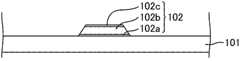
更详细地观察形成有TFT15的区域时,如图1所示,在形成有扫描配线102的玻璃基板101的主面上,被作为绝缘层的栅极绝缘膜103覆盖。在栅极绝缘膜103上,以与扫描配线102重叠的方式形成有IGZO半导体层104。在IGZO半导体层104上,形成有信号配线106和漏极电极107。TFT15被用于使保护层108和基板面平坦化的层间绝缘膜109覆盖,在层间绝缘膜109上形成有像素电极110。When the region where
TFT15包括:一部分作为栅极电极的扫描配线102、栅极绝缘膜103、作为沟道层的IGZO半导体层104、信号配线106和漏极电极107。The
这里,扫描配线102具有叠层了扫描配线层102a、102b和102c的构造。作为扫描配线102例如能够采用如下结构:是扫描配线层102a、102c含有Ti且扫描配线层102b含有Al的叠层构造,扫描配线层102a、102c的膜厚是30~150nm,扫描配线层102b的膜厚是200~500nm。Here, scanning
作为栅极绝缘膜103,能够使用氧化硅(SiOx)、氮化硅(SiNx)等无机材料,栅极绝缘膜103的膜厚例如为200~500nm左右。Inorganic materials such as silicon oxide (SiOx ) and silicon nitride (SiNx ) can be used as the
IGZO半导体层104包含IGZO半导体,该IGZO半导体包含In、Ga、Zn和O作为构成原子,在将化学计量的状态按原子单位设为100%时,具有87~95%的氧含量。通过利用具有这样的氧含量的IGZO半导体形成TFT15的沟道层,能够得到具有稳定的晶体管特性的TFT阵列基板11。IGZO半导体层104的膜厚没有特别限定,为10~300nm左右。The
信号配线106的一部分作为TFT15的源极电极起作用。作为信号配线106,例如能够列举具有叠层了信号配线层106a、106b的构造。漏极电极107具有叠层了漏极电极层107a、107b的构造。形成信号配线106和漏极电极107的材料,既可以是相同的材料,也可以是不同的材料。A part of
作为信号配线106和漏极电极107,例如能够列举具有叠层构造的结构,该叠层构造中,信号配线层106a和漏极电极层107a含有Ti,信号配线层106b和漏极电极层107b含有Al。信号配线层106a和漏极电极层107a的膜厚例如设为30~150nm左右,信号配线层106b和漏极电极层107b的膜厚例如设为50~400nm左右。As the
作为上述保护层,例如能够使用将SiOx、SiNx等无机材料利用CVD法、溅射法等进行成膜而得到的层,并且,不仅仅是SiOx膜、SiNx膜,也可以是SiOx膜和SiNx膜的叠层膜。上述层间绝缘膜例如使用感光性树脂形成。As the protective layer, for example, a layer obtained by forming a film of an inorganic material such asSiOx orSiNx by CVD, sputtering, or the like can be used, and not onlySiOx film and SiNx film but also SiOx film andSiNx film may be used. Laminated film ofx film and SiNx film. The above-mentioned interlayer insulating film is formed using, for example, a photosensitive resin.
像素电极110例如包含ITO等透明电极材料,其膜厚设为50~200nm左右。The
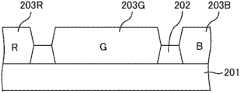
另一方面,如图1所示,CF基板13在玻璃基板201的主面上,按每个像素区域具有红(R)、蓝(B)和绿(G)的CF层203。各颜色的CF层203,由被称为黑色矩阵的遮光部(未图示)分隔开。在基板的表面,形成有厚度为50~200nm左右的对置电极204,在形成有遮光部的区域,设置有光刻型间隔物(photospacer)(未图示)。On the other hand, as shown in FIG. 1 ,
关于具有上述结构的液晶显示装置10制造方法的一例,列举具体示例进行说明。首先,关于TFT阵列基板11的制造方法的一例,使用图3~图7进行说明。图3~图7是制造本实施方式的TFT阵列基板11的各工序的截面示意图。An example of a method for manufacturing the liquid
图3表示在玻璃基板101的主面上形成有扫描配线102的状态。扫描配线102是例如利用溅射法,在玻璃基板101的主面上,依次使膜厚为30~150nm的Ti膜、膜厚为200~500nm的Al膜和膜厚为30~150nm的Ti膜成膜,形成扫描配线层102a、102b和102c,然后,将所得到的叠层膜利用包括湿蚀刻处理和抗蚀剂剥离处理的光刻法(以下,称作光刻法)图案形成为期望的形状而得到的。FIG. 3 shows a state where scanning
图4表示以栅极绝缘膜103覆盖图3所示状态的基板的主面上,进一步形成IGZO半导体层104的状态。这种状态的基板,能够通过进行绝缘膜形成工序,然后进行半导体层形成工序而得到。FIG. 4 shows a state where the main surface of the substrate shown in FIG. 3 is covered with a
在绝缘膜形成工序中,利用CVD法,以覆盖玻璃基板101和扫描配线102的方式,将SiO2堆积成厚度为200~500nm,形成栅极绝缘膜103。在半导体层形成工序中,从法线方向观察基板面时,在与扫描配线102重叠的位置形成IGZO半导体层104。In the insulating film forming step, SiO2 is deposited to a thickness of 200 to 500 nm by CVD so as to cover the
IGZO半导体层104是通过利用溅射法,使用包含In-Ga-Zn-O的靶材(target),在输出0.1~2.0kW的条件下堆积成厚度为10~300nm,并利用光刻法图案形成为期望的形状而得到的。作为靶材的组成比,例如能够列举In∶Ga∶Zn∶O=1∶1∶1∶4和In∶Ga∶Zn∶O=2∶2∶1∶7,但是本发明不限定于此,根据成膜条件适当地设定靶材的组成即可。The
图5表示配线和电极形成工序后的基板的状态。在配线和电极形成工序中,在图4所示的状态的基板,进一步形成信号配线106和漏极电极107。首先,使用溅射法,将Ti堆积成厚度为30~150nm,形成信号配线层106a和漏极电极层107a。然后,将Al堆积成厚度为50~400nm,形成信号配线层106b和漏极电极层107b。通过使用光刻法对所得到的Ti和Al的叠层膜进行图案化,形成信号配线106和漏极电极107。FIG. 5 shows the state of the substrate after the wiring and electrode forming process. In the wiring and electrode forming step,
图6表示进行了保护层形成工序和层间绝缘膜形成工序之后的基板的状态。在保护层形成工序中,利用CVD法,将SiO2堆积成厚度为100~700nm,形成覆盖信号配线106和漏极电极107的保护层108。FIG. 6 shows the state of the substrate after the protective layer forming step and the interlayer insulating film forming step are performed. In the protective layer forming step, SiO2 is deposited to a thickness of 100 to 700 nm by CVD to form the
在层间绝缘膜形成工序中,使用感光性树脂,以覆盖保护层108的方式形成层间绝缘膜109。In the interlayer insulating film forming step, a photosensitive resin is used to form the
图7表示形成像素电极110后的状态。这种状态的基板,例如是通过利用溅射法将ITO在层间绝缘膜109上堆积成厚度为50~200nm来形成薄膜,利用光刻法将该薄膜图案化为期望的形状,形成像素电极110而得到的。FIG. 7 shows the state after the
这里,在本实施方式中,在图6中的保护层形成工序与层间绝缘膜形成工序之间,还包括对保护层108进行烘焙处理的烘焙处理工序。本发明的液晶显示装置10中,IGZO半导体层104被保护层108覆盖,此后,如下所述经过层间绝缘膜形成工序将其与CF基板13贴合,由此与外部完全隔断。在这种状态下,认为IGZO半导体层104的氧脱离是发生在IGZO半导体层104与栅极绝缘膜103之间,和/或在IGZO半导体层104与保护层108之间。Here, in the present embodiment, a baking treatment step of baking the
因此,在本实施方式中,在形成保护层108之后,在各制造工序的处理温度中的最高的处理温度下进行烘焙处理。在上述各制造工序中,相对于IGZO半导体层104的形成温度是室温左右~150℃左右,在栅极绝缘膜103、保护层108和后述的层间绝缘膜109的形成时,施加约200~220℃以上的温度。因此,烘焙处理在比栅极绝缘膜103、保护层108和层间绝缘膜109的形成时更高的温度(220℃以上)下进行,控制IGZO半导体层104的氧含量。烘焙处理的方法没有特别限定,能够应用例如使用洁净烘箱(clean oven)在大气气氛中进行烘焙的简易的处理。Therefore, in the present embodiment, after the formation of the
由此,经由保护层108向IGZO半导体层104填补氧,或者从栅极绝缘膜103和保护层108向IGZO半导体层104填补氧,能够使得IGZO半导体层104的氧浓度稳定,并且在IGZO半导体层104不会发生氧脱离,实现具有期望的氧含量的IGZO半导体层104。氧含量根据要得到的晶体管特性不同而不同,但是在90%以上时化学计量上的偏差变小,能够得到稳定的晶体管特性。Thus, filling oxygen into the
使用图8~图10对CF基板13的制造方法的一例进行说明。图8~图10是表示构成实施方式1的液晶显示装置的CF基板的制造工序的平面示意图。首先,如图8所示,在玻璃基板201的主面上,利用光刻法将含有黑色颜料的感光性树脂图案化为期望的形状,形成遮光部202。然后,在由遮光部202划分的区域,涂布含有红(R)、绿(G)、蓝(B)的颜料的感光性树脂,形成CF层203R、203G、203B。An example of a method of manufacturing the
然后,如图9所示,在基板的表面,利用溅射法将ITO等透明电极材料堆积成厚度为50~200nm,利用光刻法形成具有期望的图案形状的对置电极204。进一步,如图10所示,在形成有遮光部202的区域形成光刻型间隔物205。光刻型间隔物205是使用感光性树脂,利用光刻法将其图案化为期望的形状而得到的。Next, as shown in FIG. 9 , on the surface of the substrate, a transparent electrode material such as ITO is deposited to a thickness of 50 to 200 nm by sputtering, and a
在如上所述制造出的TFT阵列基板11和CF基板13的表面,利用印刷法涂布聚酰亚胺树脂来形成取向膜(未图示)。所得到的两基板,通过密封材料被贴合,并利用滴下法、注入法等方法在基板间封入液晶。然后,通过切割来分割贴合的两基板,并根据需要设置驱动装置、箱体、光源等各种部件,能够得到本实施方式的液晶显示装置10。On the surfaces of the
在本实施方式中,如上所述,形成具有特定的原子组成的IGZO半导体,并且在形成保护层108之后,在上述制造工序的处理温度中的最高的处理温度下进行烘焙处理,因此IGZO半导体层104的氧浓度稳定,烘焙处理后在IGZO半导体层104不会发生氧脱离,由此,能够实现可靠性高的液晶显示装置10。In the present embodiment, as described above, an IGZO semiconductor having a specific atomic composition is formed, and after forming the
下面,对本实施方式的液晶显示装置10的具体例进行说明。Next, a specific example of the liquid
实施例1Example 1
在实施方式1的液晶显示装置10中,使用In∶Ga∶Zn∶O=1∶1∶1∶4的比例的溅射靶材(sputtering target),形成膜厚为50nm的IGZO半导体层。In the liquid
另外,为了控制IGZO半导体层104的氧含量,在使保护层108成膜之后,在大气中以350℃进行1个小时的烘焙处理。这里,使用洁净烘箱,在大气中以350℃的温度进行了1个小时的烘焙处理。In addition, in order to control the oxygen content of the
然后,对于从IGZO半导体层104的表面起深度约为20nm的位置上的构成原子的组成,通过AES(俄歇电子能谱,Auger ElectronSpectroscopy)分析来测定。AES分析使用AES分析装置(JEOL公司制造,型号JAMP-9500F),电子线照射条件:5kV、5nA,试样:75deg倾斜,中和条件:Ar离子10eV、1μA,检测器能量分辨率:dE/E=0.35%,检测能量步骤:在1.0eV的测定条件下进行分析,对于In、Ga、Zn、O、Si的各构成原子,求出检测峰。Then, the composition of constituent atoms at a position at a depth of about 20 nm from the surface of the
这里,对AES分析的详细情况进行说明。AES分析是对试样测定部位照射电子束,根据从表面释放的俄歇电子(auger electron)的运动能量和检测强度获得能谱。由于能谱的峰位置和形状是元素固有的,因此根据峰位置和形状能够确定元素,通过根据能谱的强度(振幅)计算材料中的元素浓度来进行元素分析。进而,由于能谱的峰位置和形状,对原子的结合状态而言也是固有的,因此也能够进行各元素中的化学结合状态(氧化状态等)的分析。Here, the details of the AES analysis will be described. In AES analysis, an electron beam is irradiated to the measurement portion of the sample, and an energy spectrum is obtained from the kinetic energy and detection intensity of the Auger electrons released from the surface. Since the peak position and shape of the energy spectrum are inherent to the element, the element can be identified based on the peak position and shape, and the elemental analysis is performed by calculating the element concentration in the material from the intensity (amplitude) of the energy spectrum. Furthermore, since the peak position and shape of the energy spectrum are also unique to the bonding state of atoms, it is also possible to analyze the chemical bonding state (oxidation state, etc.) in each element.
俄歇电子是被检测的庞大电子量中的非常小的一部分,因此显著地受到低频成分的背景影响(background influence)。在本实施例中,为了更精确地求得氧含量,除上述的AES分析之外,还进行卢瑟福背散射谱分析(RBS:Rutherford Backscattering Spectrometry)和粒子诱发X射线荧光分析(PIXE:Particle Induced X-ray Emission),使用所得到的值修正灵敏度因子。Auger electrons are a very small fraction of the large electron population being detected, and thus are significantly affected by the background influence of low frequency components. In this embodiment, in order to obtain the oxygen content more accurately, in addition to the above-mentioned AES analysis, Rutherford Backscattering Spectrometry (RBS: Rutherford Backscattering Spectrometry) and particle-induced X-ray fluorescence analysis (PIXE: Particle Induced X-ray Emission), using the resulting value to correct the sensitivity factor.
即,如通常进行的那样,对能谱进行微分,除去低频成分的背景后,根据各元素的峰强度,使用各元素固有的灵敏度因子(使用装置附属的纯元素的值)计算出组成比。基于该测定结果,通过下述公式求出氧含量。That is, after differentiating the energy spectrum and removing the background of low-frequency components as usual, the composition ratio was calculated using the sensitivity factor unique to each element (using the value of the pure element attached to the device) from the peak intensity of each element. Based on the measurement results, the oxygen content was obtained by the following formula.
另外,由于各元素的峰强度和形状在化学结合状态大幅变化时发生变化,为了以高精度求得组成比,还需要修正灵敏度因子。因此,计算组成比时,进行下述的灵敏度因子的修正。In addition, since the peak intensity and shape of each element change when the chemical bonding state changes greatly, it is also necessary to correct the sensitivity factor in order to obtain the composition ratio with high accuracy. Therefore, when calculating the composition ratio, correction of the sensitivity factor described below is performed.
具体而言,为了确认In的氧化状态、还原状态,通过以下方法计算出In(pure metal,纯金属)和In(In2O3)各自的状态的存在比。即,将利用AES分析所得到的In的微分能谱,利用非负约束最小二乘法按照In(pure metal,纯金属)和In(In2O3)的标准测定峰拟合,作为各成分进行分离,并且使用上述灵敏度因子(使用装置附属的纯元素的值)计算出成分比。Specifically, in order to confirm the oxidation state and reduction state of In, the abundance ratios of In (pure metal, pure metal) and In (In2 O3 ) states were calculated by the following method. That is, the differential spectrum of In obtained by AES analysis was fitted to the standard measurement peaks of In (pure metal, pure metal) and In (In2 O3 ) by the non-negative constrained least squares method as each component. Separate, and use the above sensitivity factors (using the values of the pure elements attached to the device) to calculate the composition ratio.
氧含量通过以下的公式求出。The oxygen content was calculated|required by the following formula.
{In(atomic%)×3/2+Ga(atomic%)×3/2+Zn(atomic%)}/O(atomic%)(atomic:原子的){In(atomic%)×3/2+Ga(atomic%)×3/2+Zn(atomic%)}/O(atomic%)(atomic: atomic)
由此,构成TFT15的沟道层的IGZO半导体的组成如图11的图表所示。另外,图11是表示构成实施例1、后述的实施例2和比较例1的TFT的沟道层的氧化物半导体的组成和氧含量的图表。Thus, the composition of the IGZO semiconductor constituting the channel layer of the
另外,测定所得到的TFT阵列基板11的TFT特性。TFT特性是基于图12所示的图表的测定结果,计算阈值(Vth)、迁移率(μ)、亚阈值摆幅(subthreshold swing,S因子)(S),并根据下述的判定基准判定出的。各判断基准需要满足所有Vth、μ和S,只要有一个不满足条件的项目,就为不合适。In addition, the TFT characteristics of the obtained
○:0v<Vth<10V,μ>5,S<1.5○: 0v<Vth<10V, μ>5, S<1.5
△:-5<Vth<10V,μ≥1,S≤2.5△: -5<Vth<10V, μ≥1, S≤2.5
×:-10<Vth<15V,μ<1,S>2.5,或无法测定(-)×: -10<Vth<15V, μ<1, S>2.5, or cannot be measured (-)
另外,图12是表示实施例1的显示装置的TFT的电气特性的图表。在图12所示的图表中,粗线表示Vg-Id特性,细线表示Vg-Id特性。另外,Vg是栅极电压,Id是漏极电流。In addition, FIG. 12 is a graph showing electrical characteristics of TFTs in the display device of Example 1. FIG. In the graph shown in FIG. 12 , thick lines represent Vg-Id characteristics, and thin lines represent Vg-Id characteristics. In addition, Vg is a gate voltage, and Id is a drain current.
得到的测定结果如图12的图表和下述表1所示。The obtained measurement results are shown in the graph of FIG. 12 and in Table 1 below.
[表1][Table 1]
实施例2Example 2
IGZO半导体的组成如图11的图表所示。另外,烘焙处理与实施例1同样地使用洁净烘箱,在220℃下进行1个小时的处理。然后,除此之外与上述实施例1同样地进行各种物性值的测定。The composition of the IGZO semiconductor is shown in the diagram of FIG. 11 . In addition, the baking process was performed at 220 degreeC for 1 hour using the clean oven similarly to Example 1. Then, the measurement of various physical property values was performed similarly to Example 1 mentioned above except this.
得到的测定结果如表1和图13所示。图13是表示实施例2的显示装置的TFT的电气特性的图表。The obtained measurement results are shown in Table 1 and FIG. 13 . 13 is a graph showing electrical characteristics of TFTs in the display device of Example 2. FIG.
比较例1Comparative example 1
IGZO半导体的组成如图11的图表所示。另外,在保护层108形成之后,不进行烘焙处理。然后,除此之外与上述实施例1同样地进行各种物性值的测定。得到的测定结果如表1和图14所示。图14是表示比较例1的显示装置的TFT的电气特性的图表。The composition of the IGZO semiconductor is shown in the diagram of FIG. 11 . In addition, after the
从表1和图12~图14所示的图表可知:实施例1和2的TFT具有优异的电气特性。另外,还可了解到:比较例1的TFT的薄膜晶体管特性差。It can be seen from Table 1 and the graphs shown in FIGS. 12 to 14 that the TFTs of Examples 1 and 2 have excellent electrical characteristics. In addition, it can also be seen that the TFT of Comparative Example 1 has poor thin film transistor characteristics.
另外,在上述实施方式中,以在对置基板的一侧设置有遮光部202和CF层为例进行了说明,但是本发明不限定于此,这些部件也能够形成在TFT阵列基板11的一侧。In addition, in the above-mentioned embodiment, the light-shielding
另外,在上述实施方式中,以使用IGZO半导体作为TFT的沟道层为例进行了说明,但是本发明不限定于此,IGZO半导体也能够应用于透明电极等。In addition, in the above-mentioned embodiments, the use of the IGZO semiconductor as the channel layer of the TFT has been described as an example, but the present invention is not limited thereto, and the IGZO semiconductor can also be applied to transparent electrodes and the like.
进而,在上述各实施方式中,以液晶显示装置为例进行了说明,但是本发明不限定于此,也能够应用于有机EL显示装置、等离子体显示装置、场发射显示装置等。Furthermore, in each of the above-mentioned embodiments, the liquid crystal display device has been described as an example, but the present invention is not limited thereto, and can also be applied to organic EL display devices, plasma display devices, field emission display devices, and the like.
上述的实施例的各方式,在不超过本发明的要旨的范围内可以适当地组合。Various aspects of the above-described embodiments can be appropriately combined within a range not exceeding the gist of the present invention.
另外,本申请以2009年6月29日提出的日本专利申请2009-154104号为基础,基于巴黎条约和进入国的法规主张优先权。该申请的全部内容在本申请中作为参照被编入。In addition, this application is based on Japanese Patent Application No. 2009-154104 filed on June 29, 2009, and claims priority based on the Treaty of Paris and the laws and regulations of the country of entry. The entire content of this application is incorporated by reference in this application.
附图标记说明Explanation of reference signs
10:液晶显示装置10: Liquid crystal display device
11:TFT阵列基板11: TFT array substrate
12:液晶层12: Liquid crystal layer
13:CF基板13: CF substrate
15:TFT15: TFT
101、201:玻璃基板101, 201: glass substrate
102a、102b、102c:扫描配线层102a, 102b, 102c: scan wiring layer
102:扫描配线102: Scan wiring
103:栅极绝缘膜103: Gate insulating film
104:氧化物半导体层104: oxide semiconductor layer
106a、106b:信号配线层106a, 106b: signal wiring layer
106:信号配线106: Signal wiring
107a、107b:漏极电极层107a, 107b: drain electrode layer
107:漏极电极107: drain electrode
108:保护层108: protective layer
109:层间绝缘膜109: Interlayer insulating film
110:像素电极110: pixel electrode
121:沟道保护层121: Channel protection layer
202:遮光部202: Shading Department
203R、203G、203B:CF203R, 203G, 203B: CF
204:对置电极204: Counter electrode
205:光刻型间隔物205: Photolithographic spacers
Claims (6)
Translated fromChineseApplications Claiming Priority (3)
| Application Number | Priority Date | Filing Date | Title |
|---|---|---|---|
| JP2009-154104 | 2009-06-29 | ||
| JP2009154104 | 2009-06-29 | ||
| PCT/JP2010/053987WO2011001715A1 (en) | 2009-06-29 | 2010-03-10 | Oxide semiconductor, thin-film transistor array substrate and manufacturing method therefor, and display device |
Publications (2)
| Publication Number | Publication Date |
|---|---|
| CN102473727Atrue CN102473727A (en) | 2012-05-23 |
| CN102473727B CN102473727B (en) | 2015-04-01 |
Family
ID=43410799
Family Applications (1)
| Application Number | Title | Priority Date | Filing Date |
|---|---|---|---|
| CN201080029375.0AActiveCN102473727B (en) | 2009-06-29 | 2010-03-10 | Oxide semiconductor, thin film transistor array substrate and production method thereof, and display device |
Country Status (4)
| Country | Link |
|---|---|
| US (2) | US8865516B2 (en) |
| JP (1) | JPWO2011001715A1 (en) |
| CN (1) | CN102473727B (en) |
| WO (1) | WO2011001715A1 (en) |
Cited By (4)
| Publication number | Priority date | Publication date | Assignee | Title |
|---|---|---|---|---|
| CN107017210A (en)* | 2016-01-08 | 2017-08-04 | 株式会社日本显示器 | Thin film transistor (TFT) |
| CN115732571A (en)* | 2021-08-31 | 2023-03-03 | 福州京东方光电科技有限公司 | Metal oxide thin film transistor, manufacturing method thereof, and display panel |
| CN111900195B (en)* | 2020-09-08 | 2023-12-19 | 京东方科技集团股份有限公司 | Display substrate, preparation method and display device thereof |
| US12432980B2 (en) | 2021-06-25 | 2025-09-30 | Boe Technology Group Co., Ltd. | Oxide thin film transistor and preparation method thereof, and display device |
Families Citing this family (12)
| Publication number | Priority date | Publication date | Assignee | Title |
|---|---|---|---|---|
| KR101812683B1 (en)* | 2009-10-21 | 2017-12-27 | 가부시키가이샤 한도오따이 에네루기 켄큐쇼 | Method for manufacturing semiconductor device |
| CN102906881B (en)* | 2010-05-21 | 2016-02-10 | 株式会社半导体能源研究所 | Semiconductor device |
| US20120032172A1 (en)* | 2010-08-06 | 2012-02-09 | Semiconductor Energy Laboratory Co., Ltd. | Semiconductor device |
| US8633044B2 (en)* | 2011-02-01 | 2014-01-21 | Sharp Kabushiki Kaisha | Display device and method for fabricating same |
| US8679905B2 (en)* | 2011-06-08 | 2014-03-25 | Cbrite Inc. | Metal oxide TFT with improved source/drain contacts |
| JP6013685B2 (en) | 2011-07-22 | 2016-10-25 | 株式会社半導体エネルギー研究所 | Semiconductor device |
| JP4982619B1 (en) | 2011-07-29 | 2012-07-25 | 富士フイルム株式会社 | Manufacturing method of semiconductor element and manufacturing method of field effect transistor |
| US9177872B2 (en)* | 2011-09-16 | 2015-11-03 | Micron Technology, Inc. | Memory cells, semiconductor devices, systems including such cells, and methods of fabrication |
| JP2014032999A (en)* | 2012-08-01 | 2014-02-20 | Panasonic Liquid Crystal Display Co Ltd | Thin film transistor and manufacturing method thereof |
| TWI566413B (en) | 2013-09-09 | 2017-01-11 | 元太科技工業股份有限公司 | Thin film transistor |
| CN104934330A (en)* | 2015-05-08 | 2015-09-23 | 京东方科技集团股份有限公司 | Film transistor and preparation method thereof, array substrate and display panel |
| US10344982B2 (en) | 2016-12-30 | 2019-07-09 | General Electric Company | Compact multi-residence time bundled tube fuel nozzle having transition portions of different lengths |
Citations (2)
| Publication number | Priority date | Publication date | Assignee | Title |
|---|---|---|---|---|
| US20060110867A1 (en)* | 2004-11-10 | 2006-05-25 | Canon Kabushiki Kaisha | Field effect transistor manufacturing method |
| WO2008126879A1 (en)* | 2007-04-09 | 2008-10-23 | Canon Kabushiki Kaisha | Light-emitting apparatus and production method thereof |
Family Cites Families (27)
| Publication number | Priority date | Publication date | Assignee | Title |
|---|---|---|---|---|
| JP4170454B2 (en) | 1998-07-24 | 2008-10-22 | Hoya株式会社 | Article having transparent conductive oxide thin film and method for producing the same |
| WO2003040441A1 (en) | 2001-11-05 | 2003-05-15 | Japan Science And Technology Agency | Natural superlattice homologous single crystal thin film, method for preparation thereof, and device using said single crystal thin film |
| JP4164562B2 (en) | 2002-09-11 | 2008-10-15 | 独立行政法人科学技術振興機構 | Transparent thin film field effect transistor using homologous thin film as active layer |
| US7297977B2 (en) | 2004-03-12 | 2007-11-20 | Hewlett-Packard Development Company, L.P. | Semiconductor device |
| US7382421B2 (en) | 2004-10-12 | 2008-06-03 | Hewlett-Packard Development Company, L.P. | Thin film transistor with a passivation layer |
| JP5126730B2 (en)* | 2004-11-10 | 2013-01-23 | キヤノン株式会社 | Method for manufacturing field effect transistor |
| AU2005302964B2 (en) | 2004-11-10 | 2010-11-04 | Canon Kabushiki Kaisha | Field effect transistor employing an amorphous oxide |
| US7791072B2 (en) | 2004-11-10 | 2010-09-07 | Canon Kabushiki Kaisha | Display |
| JP4560502B2 (en)* | 2005-09-06 | 2010-10-13 | キヤノン株式会社 | Field effect transistor |
| JP5006598B2 (en) | 2005-09-16 | 2012-08-22 | キヤノン株式会社 | Field effect transistor |
| JP5064747B2 (en) | 2005-09-29 | 2012-10-31 | 株式会社半導体エネルギー研究所 | Semiconductor device, electrophoretic display device, display module, electronic device, and method for manufacturing semiconductor device |
| EP1770788A3 (en) | 2005-09-29 | 2011-09-21 | Semiconductor Energy Laboratory Co., Ltd. | Semiconductor device having oxide semiconductor layer and manufacturing method thereof |
| JP5037808B2 (en)* | 2005-10-20 | 2012-10-03 | キヤノン株式会社 | Field effect transistor using amorphous oxide, and display device using the transistor |
| JP5000290B2 (en) | 2006-01-31 | 2012-08-15 | 出光興産株式会社 | TFT substrate and manufacturing method of TFT substrate |
| CN102244103A (en) | 2006-01-31 | 2011-11-16 | 出光兴产株式会社 | TFT substrate |
| JP2007293072A (en) | 2006-04-26 | 2007-11-08 | Epson Imaging Devices Corp | Electro-optical device manufacturing method, electro-optical device, and electronic apparatus |
| JP4609797B2 (en)* | 2006-08-09 | 2011-01-12 | Nec液晶テクノロジー株式会社 | Thin film device and manufacturing method thereof |
| JP2008140684A (en)* | 2006-12-04 | 2008-06-19 | Toppan Printing Co Ltd | Color EL display and manufacturing method thereof |
| KR101146574B1 (en)* | 2006-12-05 | 2012-05-16 | 캐논 가부시끼가이샤 | Method for manufacturing thin film transistor using oxide semiconductor and display apparatus |
| JP5197058B2 (en)* | 2007-04-09 | 2013-05-15 | キヤノン株式会社 | Light emitting device and manufacturing method thereof |
| KR101325053B1 (en)* | 2007-04-18 | 2013-11-05 | 삼성디스플레이 주식회사 | Thin film transistor substrate and manufacturing method thereof |
| KR101334181B1 (en)* | 2007-04-20 | 2013-11-28 | 삼성전자주식회사 | Thin Film Transistor having selectively crystallized channel layer and method of manufacturing the same |
| KR101334182B1 (en) | 2007-05-28 | 2013-11-28 | 삼성전자주식회사 | Fabrication method of ZnO family Thin film transistor |
| KR101345376B1 (en)* | 2007-05-29 | 2013-12-24 | 삼성전자주식회사 | Fabrication method of ZnO family Thin film transistor |
| JP4759598B2 (en) | 2007-09-28 | 2011-08-31 | キヤノン株式会社 | THIN FILM TRANSISTOR, MANUFACTURING METHOD THEREOF, AND DISPLAY DEVICE USING THE SAME |
| JP4623179B2 (en)* | 2008-09-18 | 2011-02-02 | ソニー株式会社 | Thin film transistor and manufacturing method thereof |
| KR101738996B1 (en)* | 2009-11-13 | 2017-05-23 | 가부시키가이샤 한도오따이 에네루기 켄큐쇼 | Device including nonvolatile memory element |
- 2010
- 2010-03-10JPJP2011520808Apatent/JPWO2011001715A1/enactivePending
- 2010-03-10WOPCT/JP2010/053987patent/WO2011001715A1/enactiveApplication Filing
- 2010-03-10CNCN201080029375.0Apatent/CN102473727B/enactiveActive
- 2010-03-10USUS13/377,824patent/US8865516B2/enactiveActive
- 2014
- 2014-09-05USUS14/478,055patent/US9076718B2/enactiveActive
Patent Citations (2)
| Publication number | Priority date | Publication date | Assignee | Title |
|---|---|---|---|---|
| US20060110867A1 (en)* | 2004-11-10 | 2006-05-25 | Canon Kabushiki Kaisha | Field effect transistor manufacturing method |
| WO2008126879A1 (en)* | 2007-04-09 | 2008-10-23 | Canon Kabushiki Kaisha | Light-emitting apparatus and production method thereof |
Cited By (5)
| Publication number | Priority date | Publication date | Assignee | Title |
|---|---|---|---|---|
| CN107017210A (en)* | 2016-01-08 | 2017-08-04 | 株式会社日本显示器 | Thin film transistor (TFT) |
| CN111900195B (en)* | 2020-09-08 | 2023-12-19 | 京东方科技集团股份有限公司 | Display substrate, preparation method and display device thereof |
| US12432980B2 (en) | 2021-06-25 | 2025-09-30 | Boe Technology Group Co., Ltd. | Oxide thin film transistor and preparation method thereof, and display device |
| CN115732571A (en)* | 2021-08-31 | 2023-03-03 | 福州京东方光电科技有限公司 | Metal oxide thin film transistor, manufacturing method thereof, and display panel |
| WO2023030108A1 (en)* | 2021-08-31 | 2023-03-09 | 京东方科技集团股份有限公司 | Metal oxide thin film transistor and manufacturing method therefor, and display panel |
Also Published As
| Publication number | Publication date |
|---|---|
| US9076718B2 (en) | 2015-07-07 |
| US20120091452A1 (en) | 2012-04-19 |
| CN102473727B (en) | 2015-04-01 |
| US20140367683A1 (en) | 2014-12-18 |
| WO2011001715A1 (en) | 2011-01-06 |
| US8865516B2 (en) | 2014-10-21 |
| JPWO2011001715A1 (en) | 2012-12-13 |
Similar Documents
| Publication | Publication Date | Title |
|---|---|---|
| CN102473727B (en) | Oxide semiconductor, thin film transistor array substrate and production method thereof, and display device | |
| JP7318074B2 (en) | semiconductor equipment | |
| KR101898439B1 (en) | Method for manufacturing a semiconductor device | |
| US10680117B2 (en) | Thin film transistor, method for manufacturing the same and display device comprising the same | |
| US20130320338A1 (en) | Method of manufacturing thin-film transistor, thin-film transistor, display apparatus, sensor, and digital x-ray image-capturing apparatus | |
| CN102403361A (en) | Thin Film Transistor, Method For Making The Same, Device Having The Same | |
| JP6599518B2 (en) | Thin film transistor including oxide semiconductor layer, method for manufacturing the same, and display device | |
| CN103915490A (en) | Thin film transistor, thin film transistor array panel including the same and manufacturing method thereof | |
| KR101633621B1 (en) | Field effect transistor and method for manufacturing same, display device, image sensor, and x-ray sensor | |
| JP5795551B2 (en) | Method for manufacturing field effect transistor | |
| US9773918B2 (en) | Metal oxide TFT with improved stability and mobility | |
| US20130099227A1 (en) | Oxide semiconductor, thin film transistor, and display device | |
| TWI588978B (en) | Thin film transistor and display panel | |
| US8906739B2 (en) | Thin film transistor substrate and method for manufacturing same | |
| JP5869110B2 (en) | Thin film transistor, display device, image sensor and X-ray sensor | |
| JP6928333B2 (en) | Oxide semiconductor thin film, thin film transistor, thin film transistor manufacturing method and sputtering target | |
| CN105374880B (en) | Thin film transistor and display panel | |
| CN106796888A (en) | Semiconductor devices and its manufacture method | |
| US8829513B2 (en) | Oxide semiconductor including Ga, In, Zn, and O and A thin film transistor and a display with the oxide semiconductor including Ga, In, Zn, and O | |
| US20130105788A1 (en) | Oxide semiconductor, thin film transistor, and display device | |
| CN105789216B (en) | Display panel and manufacturing method thereof |
Legal Events
| Date | Code | Title | Description |
|---|---|---|---|
| C06 | Publication | ||
| PB01 | Publication | ||
| C10 | Entry into substantive examination | ||
| SE01 | Entry into force of request for substantive examination | ||
| C14 | Grant of patent or utility model | ||
| GR01 | Patent grant |