CN102473686A - Package for containing element and mounted structure - Google Patents
Package for containing element and mounted structureDownload PDFInfo
- Publication number
- CN102473686A CN102473686ACN2010800350113ACN201080035011ACN102473686ACN 102473686 ACN102473686 ACN 102473686ACN 2010800350113 ACN2010800350113 ACN 2010800350113ACN 201080035011 ACN201080035011 ACN 201080035011ACN 102473686 ACN102473686 ACN 102473686A
- Authority
- CN
- China
- Prior art keywords
- dielectric layer
- layer
- heat transfer
- signal line
- dielectric
- Prior art date
- Legal status (The legal status is an assumption and is not a legal conclusion. Google has not performed a legal analysis and makes no representation as to the accuracy of the status listed.)
- Granted
Links
Images


Classifications
- H—ELECTRICITY
- H01—ELECTRIC ELEMENTS
- H01P—WAVEGUIDES; RESONATORS, LINES, OR OTHER DEVICES OF THE WAVEGUIDE TYPE
- H01P5/00—Coupling devices of the waveguide type
- H01P5/02—Coupling devices of the waveguide type with invariable factor of coupling
- H01P5/022—Transitions between lines of the same kind and shape, but with different dimensions
- H—ELECTRICITY
- H01—ELECTRIC ELEMENTS
- H01L—SEMICONDUCTOR DEVICES NOT COVERED BY CLASS H10
- H01L23/00—Details of semiconductor or other solid state devices
- H01L23/02—Containers; Seals
- H01L23/04—Containers; Seals characterised by the shape of the container or parts, e.g. caps, walls
- H01L23/053—Containers; Seals characterised by the shape of the container or parts, e.g. caps, walls the container being a hollow construction and having an insulating or insulated base as a mounting for the semiconductor body
- H01L23/057—Containers; Seals characterised by the shape of the container or parts, e.g. caps, walls the container being a hollow construction and having an insulating or insulated base as a mounting for the semiconductor body the leads being parallel to the base
- H—ELECTRICITY
- H01—ELECTRIC ELEMENTS
- H01L—SEMICONDUCTOR DEVICES NOT COVERED BY CLASS H10
- H01L23/00—Details of semiconductor or other solid state devices
- H01L23/552—Protection against radiation, e.g. light or electromagnetic waves
- H—ELECTRICITY
- H01—ELECTRIC ELEMENTS
- H01L—SEMICONDUCTOR DEVICES NOT COVERED BY CLASS H10
- H01L23/00—Details of semiconductor or other solid state devices
- H01L23/58—Structural electrical arrangements for semiconductor devices not otherwise provided for, e.g. in combination with batteries
- H01L23/64—Impedance arrangements
- H01L23/66—High-frequency adaptations
- H—ELECTRICITY
- H01—ELECTRIC ELEMENTS
- H01P—WAVEGUIDES; RESONATORS, LINES, OR OTHER DEVICES OF THE WAVEGUIDE TYPE
- H01P5/00—Coupling devices of the waveguide type
- H01P5/02—Coupling devices of the waveguide type with invariable factor of coupling
- H01P5/022—Transitions between lines of the same kind and shape, but with different dimensions
- H01P5/028—Transitions between lines of the same kind and shape, but with different dimensions between strip lines
- H—ELECTRICITY
- H01—ELECTRIC ELEMENTS
- H01L—SEMICONDUCTOR DEVICES NOT COVERED BY CLASS H10
- H01L2223/00—Details relating to semiconductor or other solid state devices covered by the group H01L23/00
- H01L2223/58—Structural electrical arrangements for semiconductor devices not otherwise provided for
- H01L2223/64—Impedance arrangements
- H01L2223/66—High-frequency adaptations
- H01L2223/6605—High-frequency electrical connections
- H01L2223/6627—Waveguides, e.g. microstrip line, strip line, coplanar line
- H—ELECTRICITY
- H01—ELECTRIC ELEMENTS
- H01L—SEMICONDUCTOR DEVICES NOT COVERED BY CLASS H10
- H01L2224/00—Indexing scheme for arrangements for connecting or disconnecting semiconductor or solid-state bodies and methods related thereto as covered by H01L24/00
- H01L2224/01—Means for bonding being attached to, or being formed on, the surface to be connected, e.g. chip-to-package, die-attach, "first-level" interconnects; Manufacturing methods related thereto
- H01L2224/42—Wire connectors; Manufacturing methods related thereto
- H01L2224/47—Structure, shape, material or disposition of the wire connectors after the connecting process
- H01L2224/48—Structure, shape, material or disposition of the wire connectors after the connecting process of an individual wire connector
- H01L2224/4805—Shape
- H01L2224/4809—Loop shape
- H01L2224/48091—Arched
- H—ELECTRICITY
- H01—ELECTRIC ELEMENTS
- H01L—SEMICONDUCTOR DEVICES NOT COVERED BY CLASS H10
- H01L24/00—Arrangements for connecting or disconnecting semiconductor or solid-state bodies; Methods or apparatus related thereto
- H01L24/01—Means for bonding being attached to, or being formed on, the surface to be connected, e.g. chip-to-package, die-attach, "first-level" interconnects; Manufacturing methods related thereto
- H01L24/10—Bump connectors ; Manufacturing methods related thereto
- H01L24/15—Structure, shape, material or disposition of the bump connectors after the connecting process
- H01L24/16—Structure, shape, material or disposition of the bump connectors after the connecting process of an individual bump connector
- H—ELECTRICITY
- H01—ELECTRIC ELEMENTS
- H01L—SEMICONDUCTOR DEVICES NOT COVERED BY CLASS H10
- H01L24/00—Arrangements for connecting or disconnecting semiconductor or solid-state bodies; Methods or apparatus related thereto
- H01L24/01—Means for bonding being attached to, or being formed on, the surface to be connected, e.g. chip-to-package, die-attach, "first-level" interconnects; Manufacturing methods related thereto
- H01L24/42—Wire connectors; Manufacturing methods related thereto
- H01L24/47—Structure, shape, material or disposition of the wire connectors after the connecting process
- H01L24/48—Structure, shape, material or disposition of the wire connectors after the connecting process of an individual wire connector
- H—ELECTRICITY
- H01—ELECTRIC ELEMENTS
- H01L—SEMICONDUCTOR DEVICES NOT COVERED BY CLASS H10
- H01L2924/00—Indexing scheme for arrangements or methods for connecting or disconnecting semiconductor or solid-state bodies as covered by H01L24/00
- H01L2924/0001—Technical content checked by a classifier
- H01L2924/00014—Technical content checked by a classifier the subject-matter covered by the group, the symbol of which is combined with the symbol of this group, being disclosed without further technical details
- H—ELECTRICITY
- H01—ELECTRIC ELEMENTS
- H01L—SEMICONDUCTOR DEVICES NOT COVERED BY CLASS H10
- H01L2924/00—Indexing scheme for arrangements or methods for connecting or disconnecting semiconductor or solid-state bodies as covered by H01L24/00
- H01L2924/01—Chemical elements
- H01L2924/01012—Magnesium [Mg]
- H—ELECTRICITY
- H01—ELECTRIC ELEMENTS
- H01L—SEMICONDUCTOR DEVICES NOT COVERED BY CLASS H10
- H01L2924/00—Indexing scheme for arrangements or methods for connecting or disconnecting semiconductor or solid-state bodies as covered by H01L24/00
- H01L2924/01—Chemical elements
- H01L2924/01019—Potassium [K]
- H—ELECTRICITY
- H01—ELECTRIC ELEMENTS
- H01L—SEMICONDUCTOR DEVICES NOT COVERED BY CLASS H10
- H01L2924/00—Indexing scheme for arrangements or methods for connecting or disconnecting semiconductor or solid-state bodies as covered by H01L24/00
- H01L2924/01—Chemical elements
- H01L2924/01025—Manganese [Mn]
- H—ELECTRICITY
- H01—ELECTRIC ELEMENTS
- H01L—SEMICONDUCTOR DEVICES NOT COVERED BY CLASS H10
- H01L2924/00—Indexing scheme for arrangements or methods for connecting or disconnecting semiconductor or solid-state bodies as covered by H01L24/00
- H01L2924/095—Indexing scheme for arrangements or methods for connecting or disconnecting semiconductor or solid-state bodies as covered by H01L24/00 with a principal constituent of the material being a combination of two or more materials provided in the groups H01L2924/013 - H01L2924/0715
- H01L2924/097—Glass-ceramics, e.g. devitrified glass
- H01L2924/09701—Low temperature co-fired ceramic [LTCC]
- H—ELECTRICITY
- H01—ELECTRIC ELEMENTS
- H01L—SEMICONDUCTOR DEVICES NOT COVERED BY CLASS H10
- H01L2924/00—Indexing scheme for arrangements or methods for connecting or disconnecting semiconductor or solid-state bodies as covered by H01L24/00
- H01L2924/10—Details of semiconductor or other solid state devices to be connected
- H01L2924/11—Device type
- H01L2924/12—Passive devices, e.g. 2 terminal devices
- H01L2924/1204—Optical Diode
- H01L2924/12042—LASER
- H—ELECTRICITY
- H01—ELECTRIC ELEMENTS
- H01L—SEMICONDUCTOR DEVICES NOT COVERED BY CLASS H10
- H01L2924/00—Indexing scheme for arrangements or methods for connecting or disconnecting semiconductor or solid-state bodies as covered by H01L24/00
- H01L2924/10—Details of semiconductor or other solid state devices to be connected
- H01L2924/11—Device type
- H01L2924/13—Discrete devices, e.g. 3 terminal devices
- H01L2924/1301—Thyristor
- H01L2924/13034—Silicon Controlled Rectifier [SCR]
- H—ELECTRICITY
- H01—ELECTRIC ELEMENTS
- H01L—SEMICONDUCTOR DEVICES NOT COVERED BY CLASS H10
- H01L2924/00—Indexing scheme for arrangements or methods for connecting or disconnecting semiconductor or solid-state bodies as covered by H01L24/00
- H01L2924/19—Details of hybrid assemblies other than the semiconductor or other solid state devices to be connected
- H01L2924/1901—Structure
- H01L2924/1903—Structure including wave guides
- H—ELECTRICITY
- H01—ELECTRIC ELEMENTS
- H01L—SEMICONDUCTOR DEVICES NOT COVERED BY CLASS H10
- H01L2924/00—Indexing scheme for arrangements or methods for connecting or disconnecting semiconductor or solid-state bodies as covered by H01L24/00
- H01L2924/19—Details of hybrid assemblies other than the semiconductor or other solid state devices to be connected
- H01L2924/1905—Shape
- H01L2924/19051—Impedance matching structure [e.g. balun]
- H—ELECTRICITY
- H01—ELECTRIC ELEMENTS
- H01L—SEMICONDUCTOR DEVICES NOT COVERED BY CLASS H10
- H01L2924/00—Indexing scheme for arrangements or methods for connecting or disconnecting semiconductor or solid-state bodies as covered by H01L24/00
- H01L2924/30—Technical effects
- H01L2924/301—Electrical effects
- H01L2924/3011—Impedance
- H—ELECTRICITY
- H01—ELECTRIC ELEMENTS
- H01L—SEMICONDUCTOR DEVICES NOT COVERED BY CLASS H10
- H01L2924/00—Indexing scheme for arrangements or methods for connecting or disconnecting semiconductor or solid-state bodies as covered by H01L24/00
- H01L2924/30—Technical effects
- H01L2924/301—Electrical effects
- H01L2924/3025—Electromagnetic shielding
Landscapes
- Physics & Mathematics (AREA)
- Condensed Matter Physics & Semiconductors (AREA)
- General Physics & Mathematics (AREA)
- Engineering & Computer Science (AREA)
- Computer Hardware Design (AREA)
- Microelectronics & Electronic Packaging (AREA)
- Power Engineering (AREA)
- Health & Medical Sciences (AREA)
- Electromagnetism (AREA)
- Toxicology (AREA)
- Shielding Devices Or Components To Electric Or Magnetic Fields (AREA)
- Waveguides (AREA)
- Production Of Multi-Layered Print Wiring Board (AREA)
Abstract
Translated fromChinese
Description
Translated fromChinese技术领域technical field
本发明涉及元件收纳用封装以及使用该元件收纳用封装的安装结构体。The present invention relates to a package for storing components and a mounting structure using the package for storing components.
背景技术Background technique
以往,公知有具有输入输出端子的元件收纳用封装,该输入输出端子构成为在电介质层的一主面形成信号线路、在电介质层的另一主面形成接地层(例如,日本特开平8-227949号公报)。当前正在寻求一种元件收纳用封装,即便将向信号线路传送的信号设为微波、毫米波等高频波,电磁波的泄漏也少并且高频传送特性好。Conventionally, there is known a component housing package having an input/output terminal in which a signal line is formed on one main surface of a dielectric layer and a ground layer is formed on the other main surface of the dielectric layer (for example, Japanese Patent Application Laid-Open No. Hei 8- 227949). Currently, there is a need for a package for housing components that has less leakage of electromagnetic waves and has good high-frequency transmission characteristics even if the signal transmitted to the signal line is a high-frequency wave such as microwave or millimeter wave.
发明内容Contents of the invention
本发明的目的在于提供一种高频传送特性好的元件收纳用封装以及使用该元件收纳用封装的安装结构体。An object of the present invention is to provide a package for storing components having good high-frequency transmission characteristics, and a mounting structure using the package for storing components.
本发明一实施方式的元件收纳用封装具有:在上表面具有元件的安装区域的基板;在所述基板上沿所述安装区域的外周设置且在局部具有通孔的框体。进而,元件收纳用封装还具有设置于所述通孔的输入输出端子,该输入输出端子具有:在所述框体的内外延伸的第一电介质层、形成在所述第一电介质层上且将所述框体的内外电连接的信号线路、形成在所述第一电介质层下表面的第一接地层、在平面透视下在与所述框体重叠的区域形成于所述信号线路上的第二电介质层、形成在所述第二电介质层上表面的第二接地层、设置在所述第二电介质层内且沿所述信号线路自所述框体内延伸至所述框体外的金属层。并且,所述金属层以与所述第一接地层及所述第二接地层连接的方式自所述第二电介质层形成至所述第一电介质层,并且与所述信号线路分开设置。A component housing package according to one embodiment of the present invention includes: a substrate having a component mounting region on the upper surface; and a frame provided on the substrate along the outer periphery of the mounting region and partially having a through hole. Furthermore, the device housing package further includes an input/output terminal provided in the through hole, and the input/output terminal has a first dielectric layer extending inside and outside the housing, and is formed on the first dielectric layer and covers the first dielectric layer. The signal line electrically connected inside and outside the frame, the first ground layer formed on the lower surface of the first dielectric layer, and the first ground layer formed on the signal line in the area overlapping with the frame in a plane perspective Two dielectric layers, a second ground layer formed on the upper surface of the second dielectric layer, a metal layer disposed in the second dielectric layer and extending from inside the frame to outside the frame along the signal line. In addition, the metal layer is formed from the second dielectric layer to the first dielectric layer so as to be connected to the first ground layer and the second ground layer, and is provided separately from the signal line.
另外,本发明第二实施方式的安装结构体的特征在于,具有所述元件收纳用封装和安装于所述元件收纳用封装的元件。In addition, a mounting structure according to a second embodiment of the present invention includes the component housing package and a component mounted on the component housing package.
附图说明Description of drawings
图1是本实施方式的元件收纳用封装的概要立体图。FIG. 1 is a schematic perspective view of a component housing package according to the present embodiment.
图2是本实施方式的元件收纳用封装的输入输出端子的概要立体图。FIG. 2 is a schematic perspective view of an input/output terminal of the component housing package according to the present embodiment.
图3是沿图2所示的X-X’线的输入输出端子的剖面图。Fig. 3 is a sectional view of the input/output terminal along the line X-X' shown in Fig. 2 .
图4是表示信号线路和金属层的配置关系的透射立体图。Fig. 4 is a transparent perspective view showing the arrangement relationship between signal lines and metal layers.
图5(A)是第一电介质层的分解立体图,图5(B)是第二电介质层的分解立体图。FIG. 5(A) is an exploded perspective view of the first dielectric layer, and FIG. 5(B) is an exploded perspective view of the second dielectric layer.
图6是表示一变形例的输入输出端子的概要的立体图。FIG. 6 is a perspective view showing an outline of an input/output terminal according to a modified example.
图7是沿图6所示的Y-Y’线的输入输出端子的剖面图。Fig. 7 is a sectional view of the input/output terminal along line Y-Y' shown in Fig. 6 .
图8是表示一变形例的输入输出端子的概要的立体图。FIG. 8 is a perspective view showing an outline of an input/output terminal according to a modified example.
图9是沿图8所示的Z-Z’线的第一电介质层的剖面图。Fig. 9 is a cross-sectional view of the first dielectric layer along line Z-Z' shown in Fig. 8 .
图10是表示一变形例的输入输出端子的概要的立体图。FIG. 10 is a perspective view showing an outline of an input/output terminal according to a modified example.
图11是表示一变形例的输入输出端子的概要的立体图。FIG. 11 is a perspective view showing an outline of an input/output terminal according to a modified example.
图12是沿图11所示的Yx-Y’x线的输入输出端子的剖面图。Fig. 12 is a sectional view of the input/output terminal along the line Yx-Y'x shown in Fig. 11 .
图13是一变形例的输入输出端子的剖面图。Fig. 13 is a cross-sectional view of an input/output terminal according to a modified example.
图14是一变形例的输入输出端子的剖面图。Fig. 14 is a cross-sectional view of an input/output terminal according to a modified example.
图15是一变形例的输入输出端子的剖面图。Fig. 15 is a cross-sectional view of an input/output terminal according to a modified example.
图16是表示一变形例的输入输出端子的概要的立体图。FIG. 16 is a perspective view showing an outline of an input/output terminal according to a modified example.
图17是沿图16所示的Yy-Y’y线的输入输出端子的剖面图。Fig. 17 is a sectional view of the input/output terminal along line Yy-Y'y shown in Fig. 16 .
具体实施方式Detailed ways
以下参照附图详细说明本发明的元件收纳用封装的实施方式。需要说明的是,本发明并不限于以下的实施方式。Embodiments of the component housing package of the present invention will be described in detail below with reference to the drawings. In addition, this invention is not limited to the following embodiment.
<元件收纳用封装的概略结构><Schematic Structure of Package for Component Storage>
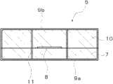
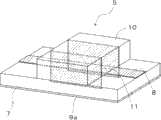
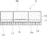
图1是表示本实施方式的元件收纳用封装1的概要立体图。图2是图1的元件收纳用封装1所使用的输入输出端子的概要立体图。元件收纳用封装1是电子器件所使用的封装。特别是,用于在微波、毫米波等高频波下使用的电子器件的高频电路。FIG. 1 is a schematic perspective view showing a
元件收纳用封装1用于安装例如由半导体元件、光半导体元件、晶体管、二极管或可控硅整流器等有源元件或者电阻器、电容器等无源元件构成的元件2。另外,将在元件收纳用封装1中安装元件2而构成的结构体作为安装结构体1X。The
元件收纳用封装1具有:在上表面具有元件2的安装区域R的基板3、在基板3上沿安装区域R的外周设置且在局部具有通孔H的框体4、设置于通孔H且将框体4内外电连接的输入输出端子5。The
基板3是俯视时形成为四边形的部件。基板3例如由铜、铁、钨、钼、镍或钴等金属材料、或者含有这些金属材料的合金制成。基板3的导热系数高,具有将由安装于安装区域R的元件2产生的热经由基板3高效地向外部散热的功能。需要说明的是,基板3的导热系数例如设定为15W/(m·K)以上450W/(m·K)以下。The
另外,对于基板3而言,使用众所周知的轧制加工或冲压加工等金属加工方法将向模框中浇铸熔融的金属材料并使其固化而形成的铸块制成规定形状。需要说明的是,基板3的一边长度例如设定为3mm以上50mm以下。而且,基板3的厚度例如设定为0.3mm以上5mm以下。In addition, for the
另外,为了防止氧化腐蚀或为了便于在安装区域R钎焊元件2,使用电镀法或无电解镀敷法在基板3的表面形成有镍或金等的电镀层。基板3的安装区域R是在将框体4与基板3的上表面连接时不与框体4连接的区域。需要说明的是,虽然在本实施方式中基板3的形状形成为四边形,但只要能够安装元件,并不限于四边形,也可以是多边形或椭圆形等。In addition, in order to prevent oxidation and corrosion or to facilitate soldering of the
框体4是如下部件:沿基板3的安装区域R的外周被连接并用于从外部保护安装于安装区域R的元件。另外,框体4在侧面的局部形成有用于设置输入输出端子5的通孔H。框体4经由钎料钎焊于基板3。需要说明的是,钎料例如由银、铜、金、铝或镁等制成,也可以含有镍、镉或磷等添加物。The
另外,框体4例如由铜、铁、钨、钼、镍或钴等金属材料、或者含有这些金属材料的合金制成。框体4具有如下功能:在元件2安装于安装区域R的状态下,将由元件2产生的热高效地向框体4的外部散热的功能。需要说明的是,框体4的导热系数例如设定为15W/(m·K)以上450W/(m·K)以下。In addition, the
在元件2安装于安装区域R的状态下,在框体4上设置有盖体6。盖体6具有将被基板2和框体4包围的空间密封的功能。盖体6例如利用钎料钎焊于框体4上。需要说明的是,盖体6例如由铜、铁、钨、钼、镍或钴等金属材料、或者含有这些金属材料的合金制成。In the state where the
在此,说明输入输出端子5。图3是沿图2所示的X-X’线的输入输出端子5的剖面图。另外,图4是表示图2所示的信号线路和金属层的配置关系的透射立体图。Here, the input/
设置于通孔H的输入输出端子5具有:在框体4的内外延伸的第一电介质层7、形成在第一电介质层7上且将框体4的内外电连接的信号线路8、形成在第一电介质层7下表面的第一接地层9a、在平面透视下在与所述框体重叠的区域形成于信号线路8上的第二电介质层10、形成在第二电介质层10上表面的第二接地层9b、设置在第二电介质层10内且沿信号线路8自框体4内延伸至框体4外的金属层11。需要说明的是,统称第一接地层9a和第二接地层9b时,称为接地层9。在此,信号线路8和接地层9成对地作为高频传送线路起作用。The input/
信号线路8具有传递规定的电信号的功能。信号线路8例如作为微波传输带线路或共面线路使用。信号线路8例如由钨、钼、锰、铜、银、金、铝、镍或铬等金属材料、或者它们的混合物、或者它们的合金等制成。信号线路8的线路宽度为传递到信号线路8的信号波长的四分之一以下,例如设定为0.05mm以上0.5mm以下。The
在信号线路8上形成有引线端子12。引线端子12是用于将外部的电子器件等和元件2电连接的部件。引线端子12利用钎料连接在信号线路8上。信号线路8和引线端子12电连接。Lead
另外,第一接地层9a形成在第一电介质层7的下表面。而且,第一接地层9a自第一电介质层7的下表面经过第一电介质层7的侧面形成至第二电介质层10的侧面。接着,上述第一接地层9a与自第二电介质层10的侧面形成至第二电介质层10上表面的第二接地层9b连接。这样,如图2或图3所示,接地层9形成在第一电介质层7及第二电介质层10的外表面。接地层9具有形成为公共电位例如接地电位的功能。另外,接地层9例如由铜、银、钨、钼、锰、金、铝、镍或铬等金属材料、或者金刚石、或者它们的混合物、或者它们的合金等制成。接地层9形成在俯视时与信号线路8重叠的区域。框体4由金属材料制成,接地层9和框体4电连接。In addition, the
第一电介质层7及第二电介质层10是绝缘性的基板,例如由氧化铝、氮化铝或氮化硅等无机材料、或者环氧树脂、聚酰亚胺树脂或乙烯树脂等有机材料、或者氧化铝或富铝红柱石等陶瓷材料、或者玻璃陶瓷材料等制成。或者,由上述材料中的多种材料混合而得到的复合系材料制成。另外,第一电介质层7及第二电介质层10的厚度为传递到信号线路8的信号波长的二分之一以下,例如设定为0.1mm以上1.0mm以下。The first
另外,第一电介质层7或第二电介质层10中也可以含有很多填料。当第一电介质层7或第二电介质层10由有机材料制成时,因第一电介质层7或第二电介质层10中含有填料,因此,可以调节第一电介质层7或第二电介质层10硬化前的粘度,可以使第一电介质层7或第二电介质层10的厚度尺寸接近所希望的值。填料为球状,填料的粒径例如设定为0.05μm以上6μm以下,热膨胀率例如为-5ppm/℃以上5ppm/℃以下。需要说明的是,填料例如由氧化硅、碳化硅、氧化铝、氮化铝或氢氧化铝等制成。In addition, many fillers may be contained in the first
另外,第一电介质层7或第二电介质层10所含有的填料的相对介电常数可以设定为比构成第一电介质层7或第二电介质层10的材料的相对介电常数小。这样,通过采用比第一电介质层7或第二电介质层10的相对介电常数小的低介电常数的填料,可以将电介质层整体进一步低介电常数化,从而可以提高向信号线路8传送的信号的传送效率。In addition, the relative permittivity of the filler contained in the first
另外,填料可以采用绝缘性填料。通过采用绝缘性填料,可以减小对传递到信号线路8的信号的特性阻抗的影响。In addition, insulating fillers can be used as fillers. By using the insulating filler, the influence on the characteristic impedance of the signal transmitted to the
在第二电介质层10内设置有金属层11。金属层11沿信号线路8自框体4内延伸至框体4外。A
金属层11自第二电介质层10的内壁面形成至第二电介质层10的外壁面。即,金属层11自被框体4包围的空间内形成至未被框体4包围的空间外。需要说明的是,金属层11例如由铜、银、钨、钼或锰等金属材料、或者金刚石、或者它们的混合物、或者它们的合金等制成。另外,金属层11的导热系数例如设定为20W/m·K以上500W/m·K以下。金属层11的厚度例如设定为0.01mm以上0.5mm以下。The
因由元件2产生的热,导致框体4内比框体4外更容易成为高温。特别是,在将微波或毫米波等高频波传送到信号线路时,存在因高频波而导致信号线路成为高温的情况。因此,框体4内的元件2的温度上升,有可能导致元件2的电气特性发生变化。金属层11自框体4内传递热,进而将传递的热向框体4外散热。其结果是,可以抑制由元件2产生的热积聚于框体4内。Due to the heat generated by the
另外,在平面透视输入输出端子5时,金属层11分别形成在信号线路8的两侧。在产生微波或毫米波等高频波时,信号线路8发热。信号线路8产生的热在剖视时以信号线路8为中心向其周围散热,因此,信号线路8所产生的热有可能积聚于框体4内。于是,通过在信号线路8的两侧分别设置金属层11,可以将信号线路8所产生的热高效地传递至金属层11。In addition, the
另外,如图3或图4所示,金属层11自第一电介质层7形成至第二电介质层10而将两者连接。而且,金属层11与信号线路8分开地设置。金属层11沿着信号线路8形成为板状,从而可以自信号线路8有效地传热。In addition, as shown in FIG. 3 or FIG. 4 , the
另外,金属层11自第二电介质层10的下端从第一电介质层7中经过并延伸至第二接地层9b。另外,金属层11还延伸至第二电介质层10的上端并与位于第二电介质层10上表面的第二接地层9b连接。而且,金属层11通过与接地层9连接而例如形成接地电位。因此,金属层11可以屏蔽基于信号线路8的高频信号产生的电场。这样,通过使金属层11具有电场屏蔽效果,可以抑制因从信号线路8产生的电场而导致元件2的高频传送特性发生变化的情况。In addition, the
另外,通过将元件2经由焊锡等突起采用倒装片方式安装于元件收纳用封装1,从而可以构成安装结构体1X。在安装IC或LSI等半导体元件时,作为半导体元件,例如可以使用硅、锗、砷化镓、磷砷化镓、氮化镓或碳化硅等。In addition, the mounting
根据本实施方式,通过设置沿信号线路8在框体4内外延伸的金属层11,可以将框体4内的热传递至框体4外,从而可以抑制框体4内的温度与框体4外的温度相比成为高温的情况,于是可以提供一种散热性好的元件收纳用封装、以及使用该元件收纳用封装的安装结构体。According to this embodiment, by providing the
在此,假设如下情况:在输入输出端子5内,俯视时自第二电介质层10的一端至另一端没有连续地形成金属层11,而是将金属层11分断,将金属层11变更为作为接地层起作用的多根金属柱。在该情况下,向信号线路8传送的信号包括被该金属柱反射而行进的信号和通过相邻的金属柱之间并被形成于第一电介质层7或第二电介质层10的侧面的接地层9反射而行进的信号。因此,在将金属层11设为多根金属柱时,在微波或毫米波等高频波中,向信号线路8传送的信号频繁地产生信号的波型变换而成为电磁波泄漏较多的信号。Here, a case is assumed in which the
另外,在替代金属层11而变更为多根金属柱时,在第一电介质层7及第二电介质层10分别形成多个通路孔后,在该通路孔中填充金属膏以形成金属柱。接着,在第一电介质层7上层叠第二电介质层10后将两层一体地烧成。但是,在假设欲形成能够应对毫米波等高频波的金属柱的情况下,通路孔必须形成为非常微细的大小。在该情况下,通路孔的孔径大小例如为0.01mm以上0.5mm以下,采用机械冲孔来设置通路孔是非常困难的,假设使用激光来设置通路孔。但是,即便使用激光,由于通路孔的孔径大小非常小,因此,控制用于设置通路孔的部位以使在俯视时在一条线上成一列地设置多个通路孔很困难。In addition, when changing to a plurality of metal pillars instead of the
另外,若设置于第一电介质层7及第二电介质层10的通路孔从所希望的部位稍稍错位,则有可能不能将第一电介质层7中的金属柱和第二电介质层10中的金属柱连接,而成为电磁波容易泄漏的结构。另外,若通路孔成为非常微细的大小,则在通路孔内部难以填充导体膏等,导致金属柱容易产生导通不良。另外,在本实施方式中,输入输出端子5非常小型,例如第一电介质层7及第二电介质层10的厚度设定为0.1mm以上1.0mm以下,因此,在例如使用激光开设通路孔时,有可能导致输入输出端子5因开设通路孔的热量而变形。这样,替代金属层11而变更为多根金属柱的结构将导致制造工序复杂、制造成品率降低。In addition, if the via holes provided in the first
而根据本实施方式,可以提供如下元件收纳用封装以及使用该元件收纳用封装的安装结构体,通过连续设置沿信号线路8在框体4内外延伸的金属层11,可以长时间确保信号的同轴波型状态,难以产生电磁波的泄漏且电气特性优越。另外,第一电介质层7及第二电介质层10可以与金属层11一起通过一体烧成来制成,从而可以简化制造工序,并且可以提高制造成品率。However, according to the present embodiment, it is possible to provide a component storage package and a mounting structure using the component storage package. By continuously providing the
<元件收纳用封装的制造方法><Manufacturing method of component housing package>
在此,说明图1所示的元件收纳用封装1及安装结构体1X的制造方法。Here, a method of manufacturing the
首先,分别准备基板3、框体4。对于基板3、框体4而言,分别使用金属加工方法将向模框浇铸熔融的金属材料并使其固化而形成的铸块制成规定形状而成。First, the
接下来,准备输入输出端子5。在此,对第一电介质层7及第二电介质层10的材料为氧化铝质烧结体、氮化铝质烧结体或富铝红柱石质烧结体等情况下的输入输出端子5的制作方法进行说明。Next, the input and
具体而言,在第一电介质层7及第二电介质层10的材料由氧化铝质烧结体构成的情况下,首先,向氧化铝、氧化硅、氧化镁及氧化钙等原料粉末中添加有机粘结剂、增塑剂或溶剂等并进行混合而形成泥浆状。Specifically, when the material of the first
接下来,准备第一电介质层7及第二电介质层10的模框。如图5(A)所示,第一电介质层7被分解为三块。这三块由在上表面形成有信号线路8且在下表面形成有接地层9的第一基体7a、以夹着信号线路8两侧的方式形成金属层11的第二基体7b、第三基体7c构成。Next, mold frames of the first
第一电介质层7的模框是第一基体7a、第二基体7b及第三基体7c各自的模框。接下来,在模框内填充泥浆状的氧化铝质材料,之后取出烧结前的第一基体7a、第二基体7b及第三基体7c。The mold of the first
如图5(B)所示,第二电介质层10被分解成三块。这三块由设置在第一基体7a上的第四基体10a、设置在第二基体7b上的第五基体10b、设置在第三基体7c上的第六基体10c构成。第二电介质层10的模框是第四基体10a、第五基体10b及第六基体10c各自的模框。接下来,在模框内填充泥浆状的氧化铝质材料,之后取出烧结前的第四基体10a、第五基体10b及第六基体10c。As shown in FIG. 5(B), the
另外,准备钨或钼等高熔点金属粉末,向该粉末中添加有机粘结剂、增塑剂或溶剂等并进行混合,从而可以得到金属膏。In addition, a metal paste with a high melting point such as tungsten or molybdenum is prepared, and an organic binder, a plasticizer, a solvent, or the like is added to the powder and mixed to obtain a metal paste.
接下来,例如使用丝网印刷法,在取出的前体的第一基体7a、第二基体7b、第三基体7c、第四基体10a、第五基体10b及第六基体10c各自的规定部位涂覆金属膏。接着,将各个基体组合来构成第一电介质层7及第二电介质层10时,所涂覆的金属膏构成信号线路8及接地层9。Next, for example, using a screen printing method, the first substrate 7a, the second substrate 7b, the third substrate 7c, the fourth substrate 10a, the fifth substrate 10b, and the sixth substrate 10c of the precursors that have been taken out are coated with Metallic paste. Next, when combining the substrates to form the first
接下来,在前体的第一电介质层7上放置前体的第二电介质层10并进行加压,从而使两者紧贴。接着,在约1600℃的温度下进行烧成,从而可以制成由陶瓷制成的输入输出端子5。Next, the precursor second
接下来,将输入输出端子5经由钎料通过钎焊与准备好的框体4的通孔H连接。通过如上所述进行处理,可以制成元件收纳用封装1。Next, the input/
接下来,在元件收纳用封装1经由焊锡安装元件2,并在框体4上设置盖体6,从而可以制成安装结构体1X。Next, the
<变形例><Modification>
本发明并不限于上述实施方式,在不脱离本发明主旨的范围内可以进行各种变更、改良等。在此,对与上述实施方式相关的变形例进行说明。需要说明的是,对于本实施方式的变形例的元件收纳用封装中与本实施方式的元件收纳用封装相同的部分,标注同一附图标记并适当省略说明。The present invention is not limited to the above-described embodiments, and various changes, improvements, and the like can be made without departing from the gist of the present invention. Here, modifications related to the above-described embodiment will be described. In addition, in the component storage package of the modification of this embodiment, the same part as the component storage package of this embodiment is attached|subjected with the same code|symbol, and description is abbreviate|omitted suitably.
<变形例1><
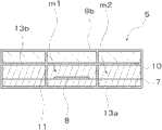
图6是变形例1的输入输出端子的概要立体图,图7是沿图6的Y-Y’线的输入输出端子的剖面图。Fig. 6 is a schematic perspective view of an input/output terminal according to
在上述实施方式中,在与信号线路8不重叠的区域设置有金属层11,但并不限于此。例如,如图6或图7所示,除金属层11之外,也可以在与信号线路8重叠的区域追加设置传热层13。In the above-described embodiment, the
传热层13设置在第一电介质层7中。传热层13自框体4内延伸至框体4外,具有将框体4内的热量传递至框体4外的功能。传热层13形成在沿着信号线路8上表面的方向上。而且,传热层13在第一电介质层7中与金属层11连接,进而与形成于第一电介质层7侧面的接地层9连接。本变形例除金属层11之外还追加有传热层13,从而可以提高散热效果。The
<变形例2><
图8是变形例2的输入输出端子的概要立体图,图9是沿图8的Z-Z’线的输入输出端子的剖面图。Fig. 8 is a schematic perspective view of an input/output terminal according to
如图8或图9所示,可以将金属层11自第二电介质层10的壁面延伸至第一电介质层7的上表面。通过将金属层11的一部分11a延伸至第一电介质层7的上表面,可以增大金属层11在框体4外露出的面积,从而可以提高金属层11的散热效果。As shown in FIG. 8 or FIG. 9 , the
另外,将金属层11的一部分11a自俯视时与第二电介质层10重叠的第一电介质层7中开始延伸至与第二电介质层10不重叠的第一电介质层7中。而且,通过在一对金属层11之间配置有信号线路8,可以逐渐改变信号线路8周围的电场屏蔽的变化。其结果是,可以抑制向信号线路8中传送的信号的电气特性的变化。In addition,
对于在信号线路8中传送的信号而言,距作为接地而起作用的层的距离越短,则越可以缩短信号被作为接地而起作用的层反射的时间,从而可以形成更高频率的信号。另一方面,在图2所示的实施方式的情况下,作为包围信号线路8的接地而起作用的金属层11并未自俯视时与第二电介质层10重叠的第一电介质层7中开延伸设置至与第二电介质层10不重叠的第一电介质层7中,因此,在俯视时与第二电介质层10重叠的第一电介质层7和与第二电介质层10不重叠的第一电介质层7之间的边界,自信号线路8朝向形成于第一电介质层7或第二电介质层10的侧面的接地层9产生电场。For the signal transmitted in the
因此,如图8或图9所示,通过使金属层11自该边界延伸至第一电介质层7中,可以将在该边界自信号线路8朝向形成于第一电介质层7或第二电介质层10的侧面的接地层9产生的电场屏蔽,从而可以使向信号线路8中传送的信号的高频传送特性良好。Therefore, as shown in FIG. 8 or FIG. 9 , by extending the
<变形例3><
图10是变形例3的输入输出端子的概要立体图,是介于第一电介质层7和第二电介质层10之间的信号线路8的透射立体图。10 is a schematic perspective view of an input/output terminal according to
如图10所示,也可以使俯视时第二电介质层10和第一电介质层7重叠的区域的信号线路8的平面方向的厚度变形。相比俯视时与第二电介质层10不重叠的区域的信号线路8的平面方向的厚度,减小俯视时与第二电介质层10重叠的区域的信号线路8的平面方向的厚度,由此可以将向信号线路8中传送的信号的电气特性设为所希望的特性。As shown in FIG. 10 , the thickness in the planar direction of the
<变形例4><
图11是变形例4的输入输出端子的概要立体图,图12是沿图11的Yx-Y’x线的输入输出端子的剖面图。Fig. 11 is a schematic perspective view of an input/output terminal according to
在上述实施方式中,使第一电介质层7或第二电介质层10内含有填料来将相对介电常数设定得小,但并不限于此。如图12所示,例如,将剖视时位于信号线路8周围的部件m1的介电常数设定为比位于该部件m1外周的部件m2的介电常数小。In the above-described embodiments, the relative permittivity is set to be small by including fillers in the first
如图12所示,部件m1在剖视时存在于被一对金属层11夹着的区域。另外,部件m1位于后述的位于上下的第一传热层13a及第二传热层13b之间。As shown in FIG. 12 , the component m1 exists in a region sandwiched by a pair of
部件m1相比部件m2而采用含有很多闭气孔的多孔材料,从而相比部件m2可以设为低介电常数。另外,部件m1通过选择介电常数比部件m2低的材料,可以谋求低介电常数化。另外,部件m1例如可以使用作为低介电常数材料的玻璃陶瓷材料等。需要说明的是,虽然本变形例的输入输出端子由多个部件构成,但例如在部件彼此的接合部位进行金属化加工或者实施镀敷后,通过钎焊、焊锡接合等可以将两部件构成一体。The member m1 uses a porous material containing many closed pores than the member m2, so that the dielectric constant can be lower than that of the member m2. In addition, the dielectric constant of the member m1 can be reduced by selecting a material having a lower dielectric constant than that of the member m2. In addition, for the member m1 , for example, a glass ceramic material, which is a low dielectric constant material, or the like can be used. It should be noted that although the input/output terminal of this modified example is composed of a plurality of parts, for example, after performing metallization processing or plating on the joining parts of the parts, the two parts can be integrally formed by brazing, soldering, or the like. .
若将向信号线路8传送的信号设为微波或毫米波等高频波,则必须减小信号线路8和金属层11之间的距离并使部件m1小型化,但通过使部件m1低介电常数化,即便将向信号线路8传送的信号设为高频,也可以增大金属层11彼此之间的距离,从而可以增大部件m1的尺寸,在制造时容易进行输入输出端子的部件处理、部件组装。If the signal transmitted to the
另外,在第一电介质层7中设置作为传热层的第一传热层13a,在第二电介质层10中设置作为传热层的第二传热层13b。第一传热层13a及第二传热层13b自框体4内延伸至框体4外,具有将框体4内的热量传递至框体4外的功能。In addition, a first
另外,在位于输入输出端子下表面的接地层9和第一传热层13a之间、或者在位于输入输出端子上表面的接地层9和第二传热层13b之间,可以设置多个通路导体14以提高接地层9和传热层13a、或者接地层9和传热层13b的接地功能的特性。通过在陶瓷生片上利用激光形成通路孔并在该通路孔印刷导体来形成通路导体14。In addition, between the
另外,在本变形例中,若将部件m1的介电常数设定为比其周围的介电常数小,则输入输出端子5也可以构成为将位于第一传热层13a下部的第一电介质层7的一部分和位于第二传热层13b上部的第二电介质层10的一部分除去。In addition, in this modified example, if the dielectric constant of the member m1 is set to be smaller than the dielectric constant of its surroundings, the input and
<变形例5><
图13是变形例5的输入输出端子的剖面图。在变形例4中,将位于一对金属层11之间的部件m1的介电常数设定为比其周围的介电常数小,但并不限于此。如图13所示,例如分别由多个层构成第一电介质层7和第二电介质层10,并且,将位于信号线路8附近的层的介电常数设定为比位于其周围的层的介电常数小。FIG. 13 is a cross-sectional view of an input/output terminal according to
在图13中,将第一电介质层7的第一传热层13a上部的介电常数设定为比第一电介质层7的第一传热层13a下层部的介电常数小,并且,将第二电介质层10的第二传热层13b下部的介电常数设定为比第二介电常数10的第二传热层13b上部的介电常数小。In FIG. 13, the dielectric constant of the upper part of the first
在第一电介质层7或第二电介质层10中,作为将位于介电常数不同的边界的层彼此连接的方法,可以预先在其边界形成通过金属化加工或镀敷等而得到的连接层,并经由该连接层一体地连接。In the first
另外,如图14所示,本变形例也可以构成为,第一电介质层7由单一层构成,第一电介质层7和第二电介质层10的第二传热层13b下部的介电常数被设定为比第一电介质层7的第二传热层13b上部的介电常数小。另外,如图15所示,也可以构成为,第二电介质层10由单一层构成,第二电介质层10和第一传热层13a上部的第一电介质层7的介电常数被设定为比第一传热层13a下部的介电常数小。In addition, as shown in FIG. 14 , in this modified example, the first
<变形例6><
图16是变形例6的输入输出端子的概要立体图,图17是沿图16的Yy-Y’y线的输入输出端子的剖面图。Fig. 16 is a schematic perspective view of an input/output terminal according to
在第一电介质层7的下表面形成有第一接地层9a。在第一电介质层7的上表面形成有第一传热层13a。因此,第一电介质层7以第一传热层13a为基准被划分为上部和下部。另外,如图17所示,在第一传热层13a的下部形成有将第一传热层13a的下部上下导通的通路导体14。A
对假设替代第一电介质层7而使用厚度与第一电介质层7的厚度相当的金属板的情况进行说明。微波或毫米波等高频波流过的输入输出端子为了抑制电磁波的影响而需要非常小型化。因此,若替代第一电介质层7而使用金属板,则很有可能因金属板和第二电介质层10之间的热膨胀系数的差异而导致第二电介质层10自金属板剥离。这样,第二电介质层10相对于金属板翘起而容易自金属板剥离。A case where a metal plate having a thickness equivalent to the thickness of the first
而根据变形例6,在第二电介质层10的下表面不使用金属体而是使用与第二电介质层10同样地由热膨胀系数相近的陶瓷材料构成的第一电介质层7,由此,即便第二电介质层10相对于第一电介质层7产生热膨胀,由于两层的热膨胀系数相近,也可以抑制第一电介质层7和第二电介质层10的剥离。According to
另外,变形例6通过在第一电介质层7的整个表面及第一电介质层7内设置多个通路导体14,可以维持第一电介质层7的接地功能,并且可以抑制第一电介质层7相对于第二电介质层10的剥离。In addition, in
Claims (8)
Applications Claiming Priority (7)
| Application Number | Priority Date | Filing Date | Title |
|---|---|---|---|
| JP2009223746 | 2009-09-29 | ||
| JP2009-223746 | 2009-09-29 | ||
| JP2009-248904 | 2009-10-29 | ||
| JP2009248904 | 2009-10-29 | ||
| JP2010-038546 | 2010-02-24 | ||
| JP2010038546 | 2010-02-24 | ||
| PCT/JP2010/066550WO2011040329A1 (en) | 2009-09-29 | 2010-09-24 | Package for containing element and mounted structure |
Publications (2)
| Publication Number | Publication Date |
|---|---|
| CN102473686Atrue CN102473686A (en) | 2012-05-23 |
| CN102473686B CN102473686B (en) | 2014-07-30 |
Family
ID=43826150
Family Applications (1)
| Application Number | Title | Priority Date | Filing Date |
|---|---|---|---|
| CN201080035011.3AExpired - Fee RelatedCN102473686B (en) | 2009-09-29 | 2010-09-24 | Package for containing element and mounted structure |
Country Status (5)
| Country | Link |
|---|---|
| US (1) | US8653649B2 (en) |
| EP (1) | EP2485253B1 (en) |
| JP (1) | JP5518086B2 (en) |
| CN (1) | CN102473686B (en) |
| WO (1) | WO2011040329A1 (en) |
Cited By (4)
| Publication number | Priority date | Publication date | Assignee | Title |
|---|---|---|---|---|
| CN104364897A (en)* | 2012-10-29 | 2015-02-18 | 京瓷株式会社 | Element-housing package and mounting structure body |
| CN104508902A (en)* | 2013-02-13 | 2015-04-08 | 株式会社村田制作所 | High frequency signal transmission line, electronic apparatus, and method for manufacturing high frequency signal transmission line |
| CN105140609A (en)* | 2015-07-13 | 2015-12-09 | 上海安费诺永亿通讯电子有限公司 | Low-loss flat transmission line |
| CN106463464A (en)* | 2014-07-30 | 2017-02-22 | 京瓷株式会社 | Package for housing electronic components and electronic device comprising same |
Families Citing this family (9)
| Publication number | Priority date | Publication date | Assignee | Title |
|---|---|---|---|---|
| CN104428888B (en)* | 2012-10-30 | 2017-09-22 | 京瓷株式会社 | Electronic unit storage container and electronic installation |
| JP2015084378A (en)* | 2013-10-25 | 2015-04-30 | キヤノン株式会社 | Electronic component, electronic apparatus, manufacturing method of mounting member, and manufacturing method of electronic component |
| US9935025B2 (en)* | 2014-03-13 | 2018-04-03 | Kyocera Corporation | Electronic component housing package and electronic device |
| JP2015192097A (en)* | 2014-03-28 | 2015-11-02 | 住友電工デバイス・イノベーション株式会社 | Package for mounting electronic component |
| US10196745B2 (en)* | 2014-10-31 | 2019-02-05 | General Electric Company | Lid and method for sealing a non-magnetic package |
| CN105025671B (en)* | 2015-07-28 | 2016-09-28 | 南京南瑞继保电气有限公司 | The shell mechanism of IGBT group unit |
| JP2017054757A (en)* | 2015-09-11 | 2017-03-16 | オムロン株式会社 | Magnetic shield structure |
| JP6809813B2 (en)* | 2016-05-30 | 2021-01-06 | 京セラ株式会社 | Semiconductor packages and semiconductor devices |
| JP7085908B2 (en)* | 2018-06-13 | 2022-06-17 | 住友電工デバイス・イノベーション株式会社 | Semiconductor device |
Citations (5)
| Publication number | Priority date | Publication date | Assignee | Title |
|---|---|---|---|---|
| US20020140071A1 (en)* | 2000-01-28 | 2002-10-03 | Larry Leighton | Multiple ground signal path LDMOS power package |
| JP2003100922A (en)* | 2001-09-27 | 2003-04-04 | Kyocera Corp | Package for storing input / output terminals and semiconductor elements |
| JP2004349568A (en)* | 2003-02-17 | 2004-12-09 | Kyocera Corp | I / O terminal and semiconductor element storage package and semiconductor device |
| JP2007150043A (en)* | 2005-11-29 | 2007-06-14 | Kyocera Corp | Semiconductor element storage package and semiconductor device |
| JP2009010149A (en)* | 2007-06-28 | 2009-01-15 | Kyocera Corp | Connection terminal, package using the same, and electronic device |
Family Cites Families (12)
| Publication number | Priority date | Publication date | Assignee | Title |
|---|---|---|---|---|
| FR2655195B1 (en)* | 1989-11-24 | 1997-07-18 | Mitsubishi Electric Corp | SEMICONDUCTOR DEVICE HAVING ELECTROMAGNETIC RADIATION SHIELDING AND MANUFACTURING METHOD. |
| JP3065416B2 (en)* | 1991-12-24 | 2000-07-17 | 新光電気工業株式会社 | Metal wall package |
| JP3185837B2 (en)* | 1994-02-21 | 2001-07-11 | 日本電信電話株式会社 | High frequency line |
| JPH08227949A (en) | 1995-02-21 | 1996-09-03 | Sumitomo Electric Ind Ltd | Metal package with high frequency terminals |
| JP3500268B2 (en)* | 1997-02-27 | 2004-02-23 | 京セラ株式会社 | High frequency input / output terminal and high frequency semiconductor element storage package using the same |
| JPH1174396A (en)* | 1997-08-28 | 1999-03-16 | Kyocera Corp | High frequency input / output terminals and high frequency semiconductor element storage package |
| JP3439969B2 (en)* | 1997-12-15 | 2003-08-25 | 京セラ株式会社 | High frequency input / output terminal and high frequency semiconductor element storage package |
| JP2001016007A (en)* | 1999-06-29 | 2001-01-19 | Ngk Spark Plug Co Ltd | Wiring board having transmission line |
| JP2001077608A (en)* | 1999-09-06 | 2001-03-23 | Toyota Motor Corp | Transmission line |
| JP2003008155A (en)* | 2001-06-19 | 2003-01-10 | Ngk Spark Plug Co Ltd | Wiring board and manufacturing method therefor |
| US6992250B2 (en)* | 2004-02-26 | 2006-01-31 | Kyocera Corporation | Electronic component housing package and electronic apparatus |
| WO2009057691A1 (en)* | 2007-10-30 | 2009-05-07 | Kyocera Corporation | Connection terminal, package using the same, and electronic device |
- 2010
- 2010-09-24JPJP2011534219Apatent/JP5518086B2/enactiveActive
- 2010-09-24WOPCT/JP2010/066550patent/WO2011040329A1/enactiveApplication Filing
- 2010-09-24EPEP10820447.0Apatent/EP2485253B1/enactiveActive
- 2010-09-24CNCN201080035011.3Apatent/CN102473686B/ennot_activeExpired - Fee Related
- 2010-09-24USUS13/391,807patent/US8653649B2/ennot_activeExpired - Fee Related
Patent Citations (5)
| Publication number | Priority date | Publication date | Assignee | Title |
|---|---|---|---|---|
| US20020140071A1 (en)* | 2000-01-28 | 2002-10-03 | Larry Leighton | Multiple ground signal path LDMOS power package |
| JP2003100922A (en)* | 2001-09-27 | 2003-04-04 | Kyocera Corp | Package for storing input / output terminals and semiconductor elements |
| JP2004349568A (en)* | 2003-02-17 | 2004-12-09 | Kyocera Corp | I / O terminal and semiconductor element storage package and semiconductor device |
| JP2007150043A (en)* | 2005-11-29 | 2007-06-14 | Kyocera Corp | Semiconductor element storage package and semiconductor device |
| JP2009010149A (en)* | 2007-06-28 | 2009-01-15 | Kyocera Corp | Connection terminal, package using the same, and electronic device |
Cited By (8)
| Publication number | Priority date | Publication date | Assignee | Title |
|---|---|---|---|---|
| CN104364897A (en)* | 2012-10-29 | 2015-02-18 | 京瓷株式会社 | Element-housing package and mounting structure body |
| CN104364897B (en)* | 2012-10-29 | 2017-07-25 | 京瓷株式会社 | Package for storing components and mounting structure |
| CN104508902A (en)* | 2013-02-13 | 2015-04-08 | 株式会社村田制作所 | High frequency signal transmission line, electronic apparatus, and method for manufacturing high frequency signal transmission line |
| CN104508902B (en)* | 2013-02-13 | 2016-08-17 | 株式会社村田制作所 | The manufacture method of high frequency signal transmission line, electronic equipment and high frequency signal transmission line |
| CN106463464A (en)* | 2014-07-30 | 2017-02-22 | 京瓷株式会社 | Package for housing electronic components and electronic device comprising same |
| CN106463464B (en)* | 2014-07-30 | 2019-02-22 | 京瓷株式会社 | Electronic component housing package and electronic device provided with the same |
| CN105140609A (en)* | 2015-07-13 | 2015-12-09 | 上海安费诺永亿通讯电子有限公司 | Low-loss flat transmission line |
| CN105140609B (en)* | 2015-07-13 | 2019-05-24 | 上海安费诺永亿通讯电子有限公司 | A kind of low-loss flat transmission line |
Also Published As
| Publication number | Publication date |
|---|---|
| CN102473686B (en) | 2014-07-30 |
| EP2485253A4 (en) | 2015-01-07 |
| WO2011040329A1 (en) | 2011-04-07 |
| EP2485253B1 (en) | 2019-12-18 |
| JP5518086B2 (en) | 2014-06-11 |
| JPWO2011040329A1 (en) | 2013-02-28 |
| US8653649B2 (en) | 2014-02-18 |
| US20120147539A1 (en) | 2012-06-14 |
| EP2485253A1 (en) | 2012-08-08 |
Similar Documents
| Publication | Publication Date | Title |
|---|---|---|
| CN102473686A (en) | Package for containing element and mounted structure | |
| CN204303794U (en) | Element storage packaging part and attachment structure | |
| CN104364897B (en) | Package for storing components and mounting structure | |
| CN104335345A (en) | Wiring board and electronic device | |
| WO2015030093A1 (en) | Package for housing elements and mounting structure | |
| CN112335034B (en) | Semiconductor devices | |
| US10249564B2 (en) | Electronic component mounting substrate, electronic device, and electronic module | |
| EP3030060B1 (en) | Wiring base plate and electronic device | |
| CN106415821B (en) | Component housing package and mounting structure | |
| CN113474884A (en) | Wiring substrate, electronic device, and electronic module | |
| JP6046421B2 (en) | Wiring board and electronic device | |
| JP2015103619A (en) | Element accommodation package and mounting structure | |
| JP6166194B2 (en) | Wiring board, electronic device and electronic module | |
| JP5334746B2 (en) | Device storage package and mounting structure | |
| JP3660817B2 (en) | Electronic circuit module | |
| US10388628B2 (en) | Electronic component package | |
| JP6166094B2 (en) | Wiring board and electronic device | |
| JP5361663B2 (en) | Device storage package and mounting structure | |
| JP5725886B2 (en) | Device storage package and mounting structure | |
| WO2015029880A1 (en) | Package for housing elements and mounting structure | |
| JP2014127589A (en) | Package for housing element and mounting structure | |
| JP2011238641A (en) | Input and output terminal, package for housing element, and packaging structure | |
| JP6595308B2 (en) | Electronic component mounting substrate, electronic device and electronic module | |
| JP2014160697A (en) | Device housing package and mounting structure | |
| JP2005159130A (en) | Wiring board |
Legal Events
| Date | Code | Title | Description |
|---|---|---|---|
| C06 | Publication | ||
| PB01 | Publication | ||
| C10 | Entry into substantive examination | ||
| SE01 | Entry into force of request for substantive examination | ||
| C14 | Grant of patent or utility model | ||
| GR01 | Patent grant | ||
| CF01 | Termination of patent right due to non-payment of annual fee | Granted publication date:20140730 Termination date:20170924 | |
| CF01 | Termination of patent right due to non-payment of annual fee |