CN102469662A - Control circuit of light emitting diode - Google Patents
Control circuit of light emitting diodeDownload PDFInfo
- Publication number
- CN102469662A CN102469662ACN2010105546644ACN201010554664ACN102469662ACN 102469662 ACN102469662 ACN 102469662ACN 2010105546644 ACN2010105546644 ACN 2010105546644ACN 201010554664 ACN201010554664 ACN 201010554664ACN 102469662 ACN102469662 ACN 102469662A
- Authority
- CN
- China
- Prior art keywords
- voltage
- target voltage
- target
- minimum terminal
- control circuit
- Prior art date
- Legal status (The legal status is an assumption and is not a legal conclusion. Google has not performed a legal analysis and makes no representation as to the accuracy of the status listed.)
- Granted
Links
Images


Landscapes
- Circuit Arrangement For Electric Light Sources In General (AREA)
- Dc-Dc Converters (AREA)
Abstract
Translated fromChinese
Description
Translated fromChinese技术领域technical field
本发明是有关于一种发光二极管的控制电路,尤指一种可转移低频调光信号所造成的噪音频率的发光二极管的控制电路。The invention relates to a control circuit of a light-emitting diode, in particular to a control circuit of a light-emitting diode capable of transferring the noise frequency caused by a low-frequency dimming signal.
背景技术Background technique
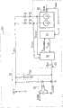
LCD的背光可以是用数串发光二极管来当光源。当平均驱动数串发光二极管时,一种已知驱动电路是大致分成两级。第一级是一固定的稳压电路,从主电流(可能是AC或是DC电源)抽取电能,用以提供一电压大致稳定的固定输出电源。举例来说,第一级可能是一电感电感电容(LLC)电源电路或是一QR(准谐振)电源电路。第二级是一电流平衡电路,用来提供大致相同的数个定电流,分别驱动数串发光二极管。图1就是一个例子。QR电源电路10作为第一级,从AC两端接收交流市电VAC。桥式整流器32将交流市电VAC整流为大概的直流VIN。变压器20有一次侧线圈(primary winding)24、二次侧线圈(secondary winding)22、以及辅助绕组(auxiliary winding)25,负责电能的储存与释放。QR控制器18控制功率开关(power switch)15。二次侧线圈(secondary winding)22所释放的电能,于输出电容13建立输出电压VOUT。输出电压VOUT,会通过分压电路12、LT431、光耦合器(photo coupler)14、以及QR控制器18,所构成的反馈回路来控制。QR电源电路10的操作、变化与原理为本领域技术人员所了解,不再多述。如图所示,电流平衡电路(current balancing circuit)30提供每一串发光二极管一个相对应的电流源,可使流经每一串发光二极管的电流大致相等。虽然图1中只有显示两串发光二极管,但是实务上需要驱动的发光二极管的串数,由系统需要而定。调光信号VDIM由DIM端控制电流平衡电路30,一般是通过改变电流源的导通周期比例(duty ratio),来控制发光二极管的亮度。The backlight of the LCD can use several strings of light-emitting diodes as the light source. When driving strings of LEDs on average, a known driving circuit is roughly divided into two stages. The first stage is a fixed voltage regulator circuit that draws power from the main current (which may be an AC or DC power supply) to provide a fixed output power supply with a roughly stable voltage. For example, the first stage may be an LLC power supply circuit or a QR (quasi-resonant) power supply circuit. The second stage is a current balance circuit, which is used to provide approximately the same constant currents to drive several strings of light-emitting diodes respectively. Figure 1 is an example. The QR
然而,实务上往往发现,在调光时,可能是因为电流源开关时的重载(heavy load)与轻载(light load)之间切换,导致QR电源电路10的工作频率的谐振,落入音频范围,有时会产生不悦耳的噪音。However, in practice, it is often found that during dimming, it may be due to the switching between heavy load and light load when the current source is switched, which causes the resonance of the operating frequency of the QR
发明内容Contents of the invention
本发明的一实施例提供一种发光二极管的控制电路。该控制电路包含一驱动器及一目标电压调整器。该驱动器用以提供一输出电源以驱动至少一串发光二极管,该驱动器可使该至少一串发光二极管的端点中的最小端点电压朝一目标电压接近;该目标电压调整器依据该最小端点电压,调整该目标电压。An embodiment of the invention provides a control circuit of a light emitting diode. The control circuit includes a driver and a target voltage regulator. The driver is used to provide an output power to drive at least one string of light-emitting diodes, the driver can make the minimum terminal voltage of the terminals of the at least one string of light-emitting diodes approach a target voltage; the target voltage regulator adjusts according to the minimum terminal voltage the target voltage.
本发明的另一实施例提供一种发光二极管的控制电路,以驱动至少一串发光二极管,该至少一串发光二极管耦接至一输出电源。该控制电路包含一最小电压反馈电路及一目标电压调整器。该最小电压反馈电路依据该至少一串发光二极管的端点中的最小端点电压以及一目标电压,来产生一调整信号,该调整信号可影响该输出电源,并使该最小端点电压接近该目标电压;及该目标电压调整器依据该最小端点电压,调整该目标电压。Another embodiment of the present invention provides a light emitting diode control circuit for driving at least one string of light emitting diodes, and the at least one string of light emitting diodes is coupled to an output power supply. The control circuit includes a minimum voltage feedback circuit and a target voltage regulator. The minimum voltage feedback circuit generates an adjustment signal according to the minimum terminal voltage among the terminals of the at least one string of light-emitting diodes and a target voltage, and the adjustment signal can affect the output power supply and make the minimum terminal voltage close to the target voltage; and the target voltage regulator adjusts the target voltage according to the minimum terminal voltage.
本发明所提供的一种发光二极管的控制电路,是通过一调整目标电压的机制来控制一往返时间所造成的噪音至60Hz或60Hz以下,远离人耳听觉的范围。The control circuit of the light-emitting diode provided by the present invention controls the noise caused by a round-trip time to 60 Hz or below 60 Hz through a mechanism of adjusting the target voltage, which is far away from the range of human hearing.
附图说明Description of drawings
图1为先前技术说明驱动发光二极管的准谐振电源电路的示意图。FIG. 1 is a schematic diagram illustrating a quasi-resonant power supply circuit for driving LEDs in the prior art.
图2为本发明的一实施例说明发光二极管的控制电路的示意图。FIG. 2 is a schematic diagram illustrating a control circuit of a light emitting diode according to an embodiment of the present invention.
图3是说明图2中,一些信号的时序图的示意图。FIG. 3 is a schematic diagram illustrating a timing diagram of some signals in FIG. 2 .
图4为本发明的另一实施例说明目标电压的切换值改变方法的流程图。FIG. 4 is a flowchart illustrating a method for changing a switching value of a target voltage according to another embodiment of the present invention.
图5为本发明的另一实施例说明目标电压的切换值改变方法的流程图。FIG. 5 is a flowchart illustrating a method for changing a switching value of a target voltage according to another embodiment of the present invention.
[主要元件标号说明][Description of main component labels]
100 控制电路 10 准谐振电源电路100
12 分压电路 13 输出电容12 Voltage divider
14 光耦合器 15 功率开关14 Optocoupler 15 Power Switch
18 准谐振控制器 20 变压器18
22 二次侧线圈 24 一次侧线圈22 Secondary side coil 24 Primary side coil
25 辅助绕组 60 最小电压反馈电路25
80 目标电压调整器 30 电流平衡电路80
32 桥式整流器 VTAR 目标电压32 Bridge Rectifier VTAR Target Voltage
VCAT-MIN 最小端点电压 VDIM 调光信号VCAT-MIN minimum terminal voltage VDIM dimming signal
VCAT1、VCATN 控制信号 ADJ 分压点VCAT1 , VCATN control signal ADJ divider point
VOUT 输出电压 IADJ、IADJ-1、IADJ-OFF 调整电流VOUT output voltage IADJ , IADJ-1 , IADJ-OFF adjustment current
VHYS 迟滞区间 T1 上升时间VHYS hysteresis interval T1 rise time
T2 下降时间 TRAMP 往返时间T2 fall time TRAMP round trip time
VTAR-HIGH 高目标电压 VTAR-LOW 低目标电压VTAR-HIGH high target voltage VTAR-LOW low target voltage
具体实施方式Detailed ways
请参照图2,图2为本发明的一实施例,例示发光二极管的控制电路100的示意图。控制电路100包含有QR(准谐振)电源电路10、最小电压反馈电路60、目标电压调整器80、以及电流平衡电路30。QR(准谐振)电源电路10、最小电压反馈电路60与电流平衡电路30一起可以视为一驱动器,来驱动数串发光二极管,使发光二极管串端点上的电压VCAT1...VCATN中的最小端点电压VCAT-MIN,朝目标电压VTAR接近或是稳定于目标电VTAR。目标电压调整器80则视调光信号VDIM与最小端点电压VCAT-MIN的状况,保持或是变更目标电VTAR。Please refer to FIG. 2 . FIG. 2 is a schematic diagram illustrating an
如同本领域技术人员所知的,QR(准谐振)电源电路10可将分压电路12中的分压点ADJ,大约地控制于接近一特定固定电压(譬如LT431所定义的2.5伏特)。当分压点ADJ的电压固定时,便可以推知输出电压VOUT的值。As known by those skilled in the art, the QR (quasi-resonant)
最小电压反馈电路60检测发光二极管串端点上的电压VCAT1...VCATN,并找出其中的最小端点电压VCAT-MIN。依据此最小端点电压VCAT-MIN,最小电压反馈电路60会决定调整电流IADJ的大小或方向。举例来说,如果最小端点电压VCAT-MIN低于目标电压VTAR,调整电流IADJ为0,此时,QR电源电路10的输出电压VOUT便往输出目标80伏特(举例说明)上升逼近,同时拉高最小端点电压VCAT-MIN。如果最小端点电压VCAT-MIN高过目标电压VTAR,调整电流IADJ为一较高的IADJ-HIGH,会使分压点ADJ的电压高过LT431所特定的2.5V。此时,为了使分压点ADJ的电压稳定在2.5V,QR电源电路10的输出电VOUT便开始下降,可能是往输出目标40伏特(举例说明)下降逼近,同时降低了最小端点电VCAT-MIN。简而言之,最小电压反馈电路60与QR电源电路10协同,使最小端点电压VCAT-MIN朝目标电压VTAR接近,或是稳定于目标电压VTAR。The minimumvoltage feedback circuit 60 detects the voltages VCAT1 . According to the minimum terminal voltage VCAT-MIN , the minimum
图3显示图2中,一些信号的时序图,用以解释一种目标电压调整器80的控制方法。图3中,由上到下,分别显示输出电压VOUT、最小端点电压VCAT-MIN、目标电压VTAR、调整电流IADJ、以及调光信号VDIM的信号波形。FIG. 3 shows a timing diagram of some signals in FIG. 2 to explain a control method of the
这里的调光信号VDIM是一数字信号,为逻辑上的“1”时,电流平衡电路30汲取电流。此时,为了要使电流平衡电路30的定电流源有足够的工作电压,所以最小端点电压VCAT-MIN至少需要有一定值。在图2的例子中,此最小值为0.8伏特。当调光信号VDIM为逻辑上的“0”,电流平衡电路30停止汲取电流,所以最小端点电压VCAT-MIN可以下降,甚至低于0.8伏特,以节省电能。The dimming signal VDIM here is a digital signal, and when it is logic “1”, the
在图3的例子中,当调光信号VDIM为逻辑上的“1”时,目标电压VTAR切换(toggle)于1V与0.8V之间。当最小端点电压VCAT-MIN低于目标电压VTAM时,目标电压调整器80使目标电压VTAR为1V;此时,调整电流IADJ为0,输出电压VOUT上升,一起提升最小端点电压VCAT-MIN,朝1V接近。当最小端点电压VCAT-MIN高于1V时,目标电压调整器80使目标电压VTAR为一0.8V;此时,调整电流IADJ为较高的IADJ-1,输出电压VOUT下降,也一起降低最小端点电压VCAT-MIN,朝0.8V接近。换言之,目标电压VTAR的迟滞区间VHYS为0.2V(=1.0V-0.8V)。In the example of FIG. 3 , when the dimming signal VDIM is logic “1”, the target voltage VTAR is toggled between 1V and 0.8V. When the minimum terminal voltage VCAT-MIN is lower than the target voltage VTAM , the
在图3的例子中,当调光信号VDIM为逻辑上的“0”时,目标电压VTAR为一比0.8V更低的值,甚至是0。此时,调整电流IADJ为IADJ-1,或是更高的IADJ-OFF。因为目标电压VTAR降低,所以输出电压VOUT便渐渐下降。In the example of FIG. 3 , when the dimming signal VDIM is logically "0", the target voltage VTAR is a value lower than 0.8V, even 0. At this time, the adjustment current IADJ is IADJ-1 , or a higher IADJ-OFF . As the target voltage VTAR decreases, the output voltage VOUT gradually decreases.
如同图3所示,最小端点电压VCAT-MIN持续增加到1.0V的时间定义为上升时间T1,持续减少到0.8V的时间定义为下降时间T2,而往返1.0V与0.8V的时间定义为往返时间TRAMP。图2中的改变目标电压VTAR的方法,只要目标电压VTAR的切换值选择适当,便可以适当的控制往返时间TRAMP的值,使其不容易产生噪音。举例来说,如果往返时间TRAMP限制在不小于16毫秒(ms),等同于频率低过人耳所能听到的60Hz的范围,噪音就不容易听的见。As shown in Figure 3, the time for the minimum terminal voltage VCAT-MIN to continuously increase to 1.0V is defined as the rising time T1 , the time for continuously decreasing to 0.8V is defined as the falling time T2 , and the time for going back and forth between 1.0V and 0.8V Defined as the round trip time TRAMP . In the method of changing the target voltage VTAR in FIG. 2 , as long as the switching value of the target voltage VTAR is selected properly, the value of the round-trip time TRAMP can be properly controlled to make it less likely to generate noise. For example, if the round-trip time TRAMP is limited to not less than 16 milliseconds (ms), which is equivalent to a frequency lower than the range of 60 Hz that can be heard by the human ear, the noise will not be easily audible.
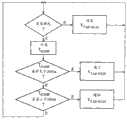
当调光信号VDIM为逻辑上的“1”时,最小端点电压VCAT-MIN随着目标电压VTAR的切换,而往高目标电压VTAR-HIGH或低目标电压VTAR-LOW逼近。图3中,高目标电压VTAR-HIGH(为1.0V)、低目标电压VTAR-LOW(为0.8V)、与迟滞区间VHYS(为0.2V)都是固定的;但是,其它的实施例中,他们可以不是固定,而是可以视情况而改变。图4显示了在另一个实施例中,目标电压VTAR的切换值改变方法。在图4的例子中,如果往返时间TRAMP高过20ms了,那就降低高目标电压VTAR-HIGH,使往返时间TRAMP减少;如果往返时间TRAMP低于16ms了,那就增加高目标电压VTAR-HIGH,使往返时间TRAMP增加。如此,往返时间TRAMP大约就会介于16~20ms之间。在另一个实施例中,可以增加或减少低目标电压VTAR-LOW,来限制往返时间TRAMP。When the dimming signal VDIM is logically "1", the minimum terminal voltage VCAT-MINapproaches the high target voltage VTAR-HIGH or the low target voltage VTAR-LOW as the target voltage V TAR switches. In Figure 3, the high target voltage VTAR-HIGH (at 1.0V), the low target voltage VTAR-LOW (at 0.8V), and the hysteresis interval VHYS (at 0.2V) are fixed; however, other implementations In some cases, they may not be fixed, but may change as the case may be. FIG. 4 shows a method for changing the switching value of the target voltage VTAR in another embodiment. In the example in Figure 4, if the round trip time TRAMP is higher than 20ms, then reduce the high target voltage VTAR-HIGH to reduce the round trip time TRAMP ; if the round trip time TRAMP is lower than 16ms, then increase the high target The voltage VTAR-HIGH increases the round trip time TRAMP . In this way, the round-trip time TRAMP will be approximately between 16-20ms. In another embodiment, the low target voltage VTAR-LOW can be increased or decreased to limit the round trip time TRAMP .
图3与图4的实施例中,最小端点电压VCAT-MIN到达了目标电压VTAR后,才改变目标电压VTAR的值。但是,在图5的实施例中,最小端点电压VCAT-MIN可以在未到达目标电压VTAR时,就改变目标电压VTAR的值。在图5的实施例中,最小端点电压VCAT-MIN往高目标电压VTAR-HIGH接近时,上升时间T1渐渐的增加。如果上升时间T1已经超过8ms,目标电压VTAR都还没有改成低目标电压VTAR-LOW时,目标电压VTAR就直接切换成低目标电压VTAR-LOW;如果上升时间T1还没有到8ms,目标电压VTAR就已经改成低目标电压VTAR-LOW,那就增加高目标电压VTAR-HIGH。如此,可以使上升时间T1,大约的限制在8ms。一样的,如果下降时间T2已经超过8ms,目标电压VTAR都还没有改成高目标电压VTAR-HIGH时,目标电压VTAR就直接切换成高目标电压VTAR-HIGH;如果下降时间T2还没有到8ms,目标电压VTAR就已经改成高目标电压VTAR-HIGH,那就降低低目标电压VTAR-LOW。如此,往返时间TRAMP就会大约地限制在16ms。In the embodiments of FIG. 3 and FIG. 4 , the value of the target voltage VTAR is changed only after the minimum terminal voltage VCAT-MIN reaches the target voltage VTAR . However, in the embodiment of FIG. 5 , the minimum terminal voltage VCAT-MIN may change the value of the target voltage VTAR when it does not reach the target voltage VTAR . In the embodiment of FIG. 5 , when the minimum terminal voltage VCAT-MIN approaches the high target voltage VTAR-HIGH , the rise time T1 gradually increases. If the rise time T1 has exceeded 8ms and the target voltage VTAR has not changed to the low target voltage VTAR-LOW , the target voltage VTAR will be directly switched to the low target voltage VTAR-LOW ; if the rise time T1 has not By 8ms, the target voltage VTAR has been changed to the low target voltage VTAR-LOW , then increase the high target voltage VTAR-HIGH . In this way, the rise time T1 can be limited to approximately 8ms. Similarly, if the falling time T2 has exceeded 8ms and the target voltage VTAR has not changed to the high target voltage VTAR-HIGH , the target voltage VTAR will be directly switched to the high target voltage VTAR-HIGH ; if the falling time T2 Before 8ms, the target voltage VTAR has been changed to the high target voltage VTAR-HIGH , then reduce the low target voltage VTAR-LOW . Thus, the round-trip time TRAMP will be limited to approximately 16ms.
以上的实施例中的第一级是以QR电源电路10为例,但是,第一级也可以以其它电源电路实施,像是LLC电源电路等。The first stage in the above embodiments is the QR
综上所述,本发明以上的实施例是通过上述调整目标电压VTAR的机制来控制往返时间TRAMP所造成的噪音至60Hz或以下,远离人耳听觉的范围。To sum up, the above embodiments of the present invention control the noise caused by the round-trip time TRAMP to 60 Hz or below through the above-mentioned mechanism of adjusting the target voltage VTAR , away from the range of human hearing.
以上所述仅为本发明的较佳实施例,凡依本发明权利要求范围所做的均等变化与修饰,皆应属本发明的涵盖范围。The above descriptions are only preferred embodiments of the present invention, and all equivalent changes and modifications made according to the claims of the present invention shall fall within the scope of the present invention.
Claims (7)
Translated fromChinesePriority Applications (1)
| Application Number | Priority Date | Filing Date | Title |
|---|---|---|---|
| CN201010554664.4ACN102469662B (en) | 2010-11-17 | 2010-11-17 | LED control circuit |
Applications Claiming Priority (1)
| Application Number | Priority Date | Filing Date | Title |
|---|---|---|---|
| CN201010554664.4ACN102469662B (en) | 2010-11-17 | 2010-11-17 | LED control circuit |
Publications (2)
| Publication Number | Publication Date |
|---|---|
| CN102469662Atrue CN102469662A (en) | 2012-05-23 |
| CN102469662B CN102469662B (en) | 2014-04-23 |
Family
ID=46072629
Family Applications (1)
| Application Number | Title | Priority Date | Filing Date |
|---|---|---|---|
| CN201010554664.4AExpired - Fee RelatedCN102469662B (en) | 2010-11-17 | 2010-11-17 | LED control circuit |
Country Status (1)
| Country | Link |
|---|---|
| CN (1) | CN102469662B (en) |
Citations (4)
| Publication number | Priority date | Publication date | Assignee | Title |
|---|---|---|---|---|
| US20040004446A1 (en)* | 2002-07-05 | 2004-01-08 | Hun-Huang Liu | Drive circuit for an led lighting apparatus |
| JP2005168129A (en)* | 2003-12-01 | 2005-06-23 | Toyota Industries Corp | Switching power supply circuit |
| US20080284346A1 (en)* | 2007-05-18 | 2008-11-20 | Samsung Electro-Mechanics Co., Ltd. | Light emitting diode array driving apparatus |
| US20100194308A1 (en)* | 2009-01-30 | 2010-08-05 | Freescale Semiconductor, Inc. | Led driver with dynamic headroom control |
- 2010
- 2010-11-17CNCN201010554664.4Apatent/CN102469662B/ennot_activeExpired - Fee Related
Patent Citations (4)
| Publication number | Priority date | Publication date | Assignee | Title |
|---|---|---|---|---|
| US20040004446A1 (en)* | 2002-07-05 | 2004-01-08 | Hun-Huang Liu | Drive circuit for an led lighting apparatus |
| JP2005168129A (en)* | 2003-12-01 | 2005-06-23 | Toyota Industries Corp | Switching power supply circuit |
| US20080284346A1 (en)* | 2007-05-18 | 2008-11-20 | Samsung Electro-Mechanics Co., Ltd. | Light emitting diode array driving apparatus |
| US20100194308A1 (en)* | 2009-01-30 | 2010-08-05 | Freescale Semiconductor, Inc. | Led driver with dynamic headroom control |
Also Published As
| Publication number | Publication date |
|---|---|
| CN102469662B (en) | 2014-04-23 |
Similar Documents
| Publication | Publication Date | Title |
|---|---|---|
| US8183795B2 (en) | LED current-supplying circuit and LED current-controlling circuit | |
| CN102548143B (en) | Drive circuit, dimmer controller and method for electrically controlling light-emitting diode (LED) light source | |
| US8044600B2 (en) | Brightness-adjustable LED driving circuit | |
| CN102076149B (en) | Light source drive circuit, controller and method for controlling light source brightness | |
| US8395329B2 (en) | LED ballast power supply having digital controller | |
| CN102740545B (en) | Constant voltage dimmable led driver | |
| CN101605416B (en) | Light-emitting diode driving circuit and its controller | |
| US8680775B2 (en) | Lighting driver circuit and light fixture | |
| US20130127356A1 (en) | Led driving power supply apparatus and led lighting apparatus | |
| JP5991614B2 (en) | Light emitting element lighting device and lighting apparatus using the same | |
| RU2628407C1 (en) | Schemes of power source | |
| US9119262B2 (en) | Boost and linear LED control | |
| US8569964B2 (en) | Control circuit of light-emitting element | |
| TW201322825A (en) | Dimmable driving systems and dimmable controllers | |
| CN109195247A (en) | Adjusting control circuit, method and the LED drive circuit using it | |
| CN102387625A (en) | Direct Drive LED Driver | |
| US7889522B2 (en) | Flyback switching power supply and control method thereof | |
| KR20090006667A (en) | Interleaved Flyback LED Drive | |
| TWI428058B (en) | Control circuit of light emitting diodes | |
| TWI458389B (en) | Dynamically adjusting dimming range driving apparatus and method thereof | |
| CN106489303A (en) | phase cut power control | |
| KR20140070126A (en) | Apparatus and method of operating the the illumination apparatus | |
| CN102469662A (en) | Control circuit of light emitting diode | |
| CN104322146A (en) | Resonant damping circuit for triac dimmable driver | |
| JP6457038B1 (en) | Low flicker LED lighting device |
Legal Events
| Date | Code | Title | Description |
|---|---|---|---|
| C06 | Publication | ||
| PB01 | Publication | ||
| C10 | Entry into substantive examination | ||
| SE01 | Entry into force of request for substantive examination | ||
| C14 | Grant of patent or utility model | ||
| GR01 | Patent grant | ||
| CF01 | Termination of patent right due to non-payment of annual fee | ||
| CF01 | Termination of patent right due to non-payment of annual fee | Granted publication date:20140423 |