CN102468284A - Stacked semiconductor device and manufacturing method thereof - Google Patents
Stacked semiconductor device and manufacturing method thereofDownload PDFInfo
- Publication number
- CN102468284A CN102468284ACN2010105407270ACN201010540727ACN102468284ACN 102468284 ACN102468284 ACN 102468284ACN 2010105407270 ACN2010105407270 ACN 2010105407270ACN 201010540727 ACN201010540727 ACN 201010540727ACN 102468284 ACN102468284 ACN 102468284A
- Authority
- CN
- China
- Prior art keywords
- wafer
- active
- components
- wafer assembly
- conductive
- Prior art date
- Legal status (The legal status is an assumption and is not a legal conclusion. Google has not performed a legal analysis and makes no representation as to the accuracy of the status listed.)
- Granted
Links
Images


Classifications
- H—ELECTRICITY
- H10—SEMICONDUCTOR DEVICES; ELECTRIC SOLID-STATE DEVICES NOT OTHERWISE PROVIDED FOR
- H10D—INORGANIC ELECTRIC SEMICONDUCTOR DEVICES
- H10D88/00—Three-dimensional [3D] integrated devices
- H—ELECTRICITY
- H01—ELECTRIC ELEMENTS
- H01L—SEMICONDUCTOR DEVICES NOT COVERED BY CLASS H10
- H01L24/00—Arrangements for connecting or disconnecting semiconductor or solid-state bodies; Methods or apparatus related thereto
- H01L24/80—Methods for connecting semiconductor or other solid state bodies using means for bonding being attached to, or being formed on, the surface to be connected
- H—ELECTRICITY
- H01—ELECTRIC ELEMENTS
- H01L—SEMICONDUCTOR DEVICES NOT COVERED BY CLASS H10
- H01L2224/00—Indexing scheme for arrangements for connecting or disconnecting semiconductor or solid-state bodies and methods related thereto as covered by H01L24/00
- H01L2224/80—Methods for connecting semiconductor or other solid state bodies using means for bonding being attached to, or being formed on, the surface to be connected
- H01L2224/80001—Methods for connecting semiconductor or other solid state bodies using means for bonding being attached to, or being formed on, the surface to be connected by connecting a bonding area directly to another bonding area, i.e. connectorless bonding, e.g. bumpless bonding
- H01L2224/80003—Methods for connecting semiconductor or other solid state bodies using means for bonding being attached to, or being formed on, the surface to be connected by connecting a bonding area directly to another bonding area, i.e. connectorless bonding, e.g. bumpless bonding involving a temporary auxiliary member not forming part of the bonding apparatus
- H01L2224/80006—Methods for connecting semiconductor or other solid state bodies using means for bonding being attached to, or being formed on, the surface to be connected by connecting a bonding area directly to another bonding area, i.e. connectorless bonding, e.g. bumpless bonding involving a temporary auxiliary member not forming part of the bonding apparatus being a temporary or sacrificial substrate
- H—ELECTRICITY
- H01—ELECTRIC ELEMENTS
- H01L—SEMICONDUCTOR DEVICES NOT COVERED BY CLASS H10
- H01L2924/00—Indexing scheme for arrangements or methods for connecting or disconnecting semiconductor or solid-state bodies as covered by H01L24/00
- H01L2924/15—Details of package parts other than the semiconductor or other solid state devices to be connected
- H01L2924/151—Die mounting substrate
- H01L2924/156—Material
- H01L2924/15786—Material with a principal constituent of the material being a non metallic, non metalloid inorganic material
- H01L2924/15788—Glasses, e.g. amorphous oxides, nitrides or fluorides
Landscapes
- Engineering & Computer Science (AREA)
- Computer Hardware Design (AREA)
- Microelectronics & Electronic Packaging (AREA)
- Power Engineering (AREA)
- Internal Circuitry In Semiconductor Integrated Circuit Devices (AREA)
Abstract
Translated fromChinese
Description
Translated fromChinese技术领域technical field
本发明涉及半导体器件及其制造方法,更具体地,涉及利用贯穿通道(through wafer vias,缩写为TWV)提供的堆叠的半导体器件以及利用贯穿通道互连不同层面(level)的半导体器件的方法。The present invention relates to a semiconductor device and a manufacturing method thereof, more particularly, to a stacked semiconductor device provided by a through wafer vias (abbreviated as TWV) and a method for interconnecting semiconductor devices of different levels by using the through wafer vias.
背景技术Background technique
半导体器件的一个重要发展趋势是减小半导体器件的芯片占用面积(footprint)。利用半导体器件的三维集成,即在垂直于晶片的方向上堆叠多个层面的半导体器件,可以成倍地提高器件的集成度,从而实现器件的小型化和性能的改善。An important development trend of semiconductor devices is to reduce the chip footprint of semiconductor devices. Using three-dimensional integration of semiconductor devices, that is, stacking multiple layers of semiconductor devices in the direction perpendicular to the wafer, can double the integration of devices, thereby achieving miniaturization and performance improvement of devices.
通常,在各个层面的晶片中直接形成贯穿通道,使得堆叠的晶片利用贯穿通道而电连接和物理连接在一起。贯穿通道的制造步骤包括在硅晶片中通过刻蚀和背侧研磨形成贯穿孔、通过热氧化等在贯穿孔壁上形成绝缘层、以及通道金属填充。在形成贯穿通道之后,将包含有源器件和贯穿通道的晶片转移至临时的载片上,以便与其他层面的晶片键合。Usually, through-vias are directly formed in the wafers at each level, so that stacked wafers are electrically and physically connected together using the through-vias. The manufacturing steps of the through-via include forming a through-hole in a silicon wafer by etching and backside grinding, forming an insulating layer on the wall of the through-hole by thermal oxidation, etc., and filling the through-hole with metal. After the through-vias are formed, the wafer containing the active devices and the through-vias is transferred to a temporary carrier for bonding to other layers of the wafer.
为了形成贯穿通道,各个层面的晶片的厚度受到限制。如果晶片过薄,则机械强度小,在转移至载片时容易发生破裂;如果晶片过厚,则贯穿孔的深宽比过大,在刻蚀步骤中难以完全刻蚀去除,进而在最终的半导体器件中可能发生互连的开路。In order to form through channels, the thickness of the wafer at each level is limited. If the wafer is too thin, the mechanical strength is low, and it is easy to crack when transferred to the carrier; if the wafer is too thick, the aspect ratio of the through hole is too large, and it is difficult to completely etch and remove it in the etching step, and then in the final Open circuits of interconnections may occur in semiconductor devices.
因此,在上述常规的三维集成的半导体器件中,还存在着器件可靠性差、制造产率低、以及在贯穿通道附近存在应力集中而影响劣化器件的性能的问题。Therefore, in the above-mentioned conventional three-dimensional integrated semiconductor devices, there are also problems of poor device reliability, low manufacturing yield, and stress concentration near the through channel, which affects the performance of the degraded device.
发明内容Contents of the invention
本发明的目的是提供一种改进的堆叠的半导体器件及其制造方法,其中减少了贯穿通道对堆叠的半导体器件的设计限制和对其性能的不利影响。It is an object of the present invention to provide an improved stacked semiconductor device and method of manufacturing the same, in which the design constraints and adverse effects of through vias on the stacked semiconductor device and its performance are reduced.
根据本发明的一方面,提供一种堆叠的半导体器件,包括:半导体衬底,以及位于半导体衬底上的多个层面的晶片组件,其中,每一层面的晶片组件包括有源部件和键合部件,其中,有源部件和键合部件分别包括彼此垂直地对齐的贯穿导电通道,使得每一个层面的有源部件利用贯穿导电通道与下一层面/上一层面的有源部件电连接。According to one aspect of the present invention, there is provided a stacked semiconductor device, comprising: a semiconductor substrate, and a wafer assembly at multiple levels on the semiconductor substrate, wherein the wafer assembly at each level includes active components and bonding components, wherein the active components and the bonding components respectively include penetrating conductive channels vertically aligned with each other, so that the active components of each level are electrically connected to the active components of the next/upper layer by using the penetrating conductive channels.
根据本发明的另一方面,提供一种制造堆叠的半导体器件的方法,包括以下步骤:According to another aspect of the present invention, there is provided a method of manufacturing a stacked semiconductor device, comprising the steps of:
a)提供包括互连晶片和有源晶片的晶片组件,其中互连晶片包括玻璃衬底、位于玻璃衬底上的互连部件,该互连部件包括贯穿导电通道,有源晶片包括半导体衬底、位于半导体衬底上的有源部件,该有源部件包括贯穿导电通道;a) providing a wafer assembly comprising an interconnect wafer comprising a glass substrate, an interconnect component on the glass substrate, the interconnect component comprising through conductive vias, and an active wafer comprising a semiconductor substrate . An active component on a semiconductor substrate, the active component comprising a through-conducting via;
b)去除第一晶片组件中的玻璃衬底;b) removing the glass substrate in the first wafer assembly;
c)去除第二晶片组件中的半导体衬底;c) removing the semiconductor substrate in the second wafer assembly;
d)将第一晶片组件与第二晶片组件直接晶片键合,使得第一晶片组件中的有源部件的贯穿导电通道与第二晶片组件中的键合部件的贯穿导电通道电连接;d) direct wafer bonding of the first wafer assembly to the second wafer assembly such that the through conductive paths of the active components in the first wafer assembly are electrically connected with the through conductive paths of the bonded components in the second wafer assembly;
e)去除第二晶片组件中的玻璃衬底;e) removing the glass substrate in the second wafer assembly;
f)重复步骤c)-e),堆叠多个层面的晶片组件。f) Steps c)-e) are repeated to stack wafer assemblies of multiple levels.
根据本发明的又一方面,提供一种制造堆叠的半导体器件方法,包括以下步骤:According to yet another aspect of the present invention, there is provided a method of manufacturing a stacked semiconductor device, comprising the following steps:
a)提供包括互连晶片和有源晶片的晶片组件,其中互连晶片包括玻璃衬底、位于玻璃衬底上的互连部件,该互连部件包括贯穿导电通道,有源晶片包括半导体衬底、位于半导体衬底上的有源部件,该有源部件包括贯穿导电通道;a) providing a wafer assembly comprising an interconnect wafer comprising a glass substrate, an interconnect component on the glass substrate, the interconnect component comprising through conductive vias, and an active wafer comprising a semiconductor substrate . An active component on a semiconductor substrate, the active component comprising a through-conducting via;
b)去除第一晶片组件中的半导体衬底;b) removing the semiconductor substrate in the first wafer assembly;
c)去除第二晶片组件中的玻璃衬底;c) removing the glass substrate in the second wafer assembly;
d)将第一晶片组件与第二晶片组件直接晶片键合,使得第一晶片组件中的有源部件的贯穿导电通道与第二晶片组件中的键合部件的贯穿导电通道电连接;d) direct wafer bonding of the first wafer assembly to the second wafer assembly such that the through conductive paths of the active components in the first wafer assembly are electrically connected with the through conductive paths of the bonded components in the second wafer assembly;
e)去除第二晶片组件中的半导体衬底;e) removing the semiconductor substrate in the second wafer assembly;
f)重复步骤c)-e),堆叠多个层面的晶片组件;f) repeating steps c)-e), stacking chip components of multiple levels;
g)重复步骤c)-d),堆叠最底层的晶片组件;g) repeating steps c)-d), stacking the lowest chip assembly;
h)去除最顶层的晶片组件中的玻璃衬底。h) Removing the glass substrate in the topmost wafer assembly.
由于晶片组件包括键合在一起的互连晶片和有源晶片,因此可以减小有源部件的厚度,从而可以容易地在有源部件中形成贯穿孔,降低半导体器件的制造成本。Since the wafer assembly includes the interconnection wafer and the active wafer bonded together, the thickness of the active components can be reduced, so that through holes can be easily formed in the active components, reducing the manufacturing cost of semiconductor devices.
而且,在直接晶片键合步骤中,互连部件为有源晶片中的有源部件提供了支撑和保护作用,这提高了制造的产率和半导体器件的可靠性。此外,还可以实现互连晶片的标准化,以进一步降低半导体器件的制造成本。Furthermore, the interconnection features provide support and protection for active components in the active wafer during the direct wafer bonding step, which improves manufacturing yield and reliability of semiconductor devices. In addition, standardization of interconnected wafers can be achieved to further reduce the manufacturing cost of semiconductor devices.
附图说明Description of drawings
图1至3示出了在根据本发明的制造堆叠的半导体器件的方法中形成晶片组件的各个阶段的截面图。1 to 3 show cross-sectional views of various stages of forming a wafer assembly in a method of manufacturing a stacked semiconductor device according to the present invention.
图4至6示出了在根据本发明的制造堆叠的半导体器件的方法的第一实施例中堆叠晶片组件的各个阶段的截面图。4 to 6 show cross-sectional views of various stages of a stacked wafer assembly in the first embodiment of the method of manufacturing a stacked semiconductor device according to the present invention.
图7至9示出了在根据本发明的制造堆叠的半导体器件的方法的第二实施例中堆叠晶片组件的各个阶段的截面图。7 to 9 show cross-sectional views of various stages of a stacked wafer assembly in a second embodiment of the method of manufacturing a stacked semiconductor device according to the present invention.
图10示出了根据本发明的堆叠的半导体器件的截面图。Fig. 10 shows a cross-sectional view of a stacked semiconductor device according to the present invention.
具体实施方式Detailed ways
以下将参照附图更详细地描述本发明。在各个附图中,相同的元件采用类似的附图标记来表示。为了清楚起见,附图中的各个部分没有按比例绘制。Hereinafter, the present invention will be described in more detail with reference to the accompanying drawings. In the various figures, identical elements are indicated with similar reference numerals. For the sake of clarity, various parts in the drawings have not been drawn to scale.
应当理解,在描述半导体器件的结构时,当将一层、一个区域称为位于另一层、另一个区域“上面”或“上方”时,可以指直接位于另一层、另一个区域上面,或者在其与另一层、另一个区域之间还包含其它的层或区域。并且,如果将器件翻转,该一层、一个区域将位于另一层、另一个区域“下面”或“下方”。It should be understood that when describing the structure of a semiconductor device, when a layer or a region is referred to as being "on" or "over" another layer or another region, it may mean being directly on another layer or another region, Or other layers or regions are included between it and another layer or another region. And, if the device is turned over, the layer, one region, will be "below" or "beneath" the other layer, another region.
如果为了描述直接位于另一层、另一个区域上面的情形,本文将采用“直接在......上面”或“在......上面并与之邻接”的表述方式。If it is to describe the situation of being directly on another layer or another area, the expression "directly on" or "on and adjacent to" will be used herein.
在本申请中,术语“半导体结构”指在制造半导体器件的各个步骤中形成的整个半导体结构的统称,包括已经形成的所有层或区域。In the present application, the term "semiconductor structure" refers to a general designation of the entire semiconductor structure formed in various steps of manufacturing a semiconductor device, including all layers or regions that have been formed.
在下文中还描述了本发明的许多特定的细节,例如半导体器件的结构、材料、尺寸、处理工艺和技术,以便更清楚地理解本发明。但正如本领域的技术人员能够理解的那样,可以不按照这些特定的细节来实现本发明。Many specific details of the present invention, such as structures, materials, dimensions, processing techniques and techniques of semiconductor devices, are also described below for a clearer understanding of the present invention. However, the invention may be practiced without these specific details, as will be understood by those skilled in the art.
除非在下文中特别指出,半导体器件中的各个部分可以由本领域的技术人员公知的材料构成。Unless otherwise specified below, various parts in the semiconductor device may be composed of materials known to those skilled in the art.
尽管以下示出的步骤应用于半导体工艺的后段工艺(BEOL),其中在形成互连和导线期间形成贯穿晶片的通道,用于连接各个层面的晶片,然而,应当理解,类似的步骤也可以容易地应用于半导体芯片的封装工艺中,其中贯穿芯片的通道用于连接各个层面的芯片。Although the steps shown below apply to the back-end-of-line (BEOL) of semiconductor processing, where through-wafer vias are formed during the formation of interconnects and wires for connecting wafers at various levels, it should be understood that similar steps can also be It is easily applied in the packaging process of semiconductor chips, where through-chip channels are used to connect chips at various levels.
按照本发明的方法的优选实施例,依次执行图1至6所示的用于制造堆叠的半导体器件的各个步骤。According to a preferred embodiment of the method of the invention, the individual steps for manufacturing a stacked semiconductor device shown in FIGS. 1 to 6 are performed in sequence.
参见图1,本发明的示例方法开始于已经完成CMOS(互补型金属氧化物半导体晶体管)工艺的前段工艺(FEOL)的常规半导体结构。Referring to FIG. 1 , the exemplary method of the present invention starts with a conventional semiconductor structure that has completed the front end of the line (FEOL) of a CMOS (complementary metal oxide semiconductor transistor) process.
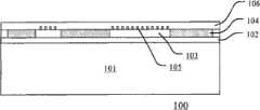
有源晶片100包括半导体衬底101、位于半导体衬底101上的第一绝缘层102、位于第一绝缘层102上的多个有源区103、用于隔离各个有源区103的第二绝缘层104、以及覆盖多个有源区103和第二绝缘层的第三绝缘层106。在每一个有源区103中形成了多个晶体管,应当注意,在图1中仅示出了晶体管的栅极105。在每一个栅极的两侧,已经在前段工艺中利用离子注入形成了源/漏区等掺杂的区域(未示出)。The
第一绝缘层102和第三绝缘层106可以由常规的层间电介质(IDL)材料构成,第二绝缘层104可以由常规的浅沟隔离(STI)材料构成。正如下文将提及的,第一绝缘层102和第三绝缘层106还应当适合于应用直接键合工艺。The first
优选地,为了获得均匀的图案密度,栅极105中的一部分可以是假栅极,其中没有提供完整的有源器件。Preferably, in order to obtain a uniform pattern density, a part of the
进一步优选地,根据设计需要,假栅极既可以分布在有源区103上,也可以分布在第二绝缘层104上(参见后面的图5)。Further preferably, according to design requirements, the dummy gates can be distributed on the
接着,按照如下的步骤在有源晶片100中形成导电通道107。Next, the
首先,在图1的半导体结构的表面上设置形成有图案的光抗蚀剂掩模(未示出)。First, a patterned photoresist mask (not shown) is disposed on the surface of the semiconductor structure of FIG. 1 .
然后,通过干法刻蚀,如离子铣刻蚀、等离子刻蚀、反应离子刻蚀、激光烧蚀,或者通过其中使用刻蚀剂溶液的湿法刻蚀,去除第一绝缘层102、第二绝缘层104和第三绝缘层106的暴露部分,该刻蚀停止在半导体衬底101的顶部表面上,从而形成贯穿第一绝缘层102、第二绝缘层104和第三绝缘层106的孔。Then, by dry etching, such as ion milling etching, plasma etching, reactive ion etching, laser ablation, or by wet etching in which an etchant solution is used, the first insulating
然后,通过在溶剂中溶解或灰化去除光抗蚀剂掩模(未示出)。Then, the photoresist mask (not shown) is removed by dissolving in a solvent or ashing.
然后,通过已知的淀积工艺,如PVD、CVD、原子层淀积、溅射等,在孔中填充导电材料(如Cu、W等)。Then, a conductive material (such as Cu, W, etc.) is filled in the hole by a known deposition process, such as PVD, CVD, atomic layer deposition, sputtering, etc.
最后,通过化学机械平面化(CMP)平整半导体结构的表面,去除通道周围的导电材料,从而形成贯穿第一绝缘层102、第二绝缘层104和第三绝缘层106的导电通道107,如图2所示。Finally, the surface of the semiconductor structure is flattened by chemical mechanical planarization (CMP), and the conductive material around the channel is removed, thereby forming a
代替地,导电通道107也可以位于有源区103中,即贯穿有源层。为此,在上述形成孔的步骤之后,还包括附加的氧化步骤,在孔的内壁形成绝缘层,使得导电通道107与有源区103中的其他元件电隔离。Alternatively, the
典型地,第一绝缘层102、第二绝缘层104和第三绝缘层106的总厚度约为0.1um~1um。Typically, the total thickness of the first insulating
接着,参见图3,利用直接晶片键合工艺,将互连晶片200与有源晶片100键合。例如,在直接晶片键合工艺中采用的温度低于200℃。在该键合步骤中,有源晶片100的导电通道107与键合晶片的导电通道203电连接。Next, referring to FIG. 3 , the
键合晶片200包括玻璃衬底201、在玻璃衬底201上形成的第四绝缘层202、以及在第四绝缘层202中形成的导电通道203。导电通道203贯穿第四绝缘层202。第四绝缘层202可以包括任何绝缘介质薄膜(如有机多聚酯物等),导电通道203可以包括任何导体(金属,碳纳米管等)。The bonded
第四绝缘层202的厚度为10um~100um的范围,使得在随后的减薄和转移工艺中,键合晶片200可以提供支撑有源晶片100所需的机械强度。The fourth insulating
优选地,可以采用上述已知的淀积工艺在玻璃衬底201上形成第四绝缘层202,可以采用上述用于形成导电通道107类似的工艺在第四绝缘层202中形成导电通道203。Preferably, the above-mentioned known deposition process can be used to form the fourth insulating
在最终的半导体器件中,第四绝缘层202将分别第一绝缘层102、第三绝缘层106直接键合,因此,第一绝缘层102、第三绝缘层104和第四绝缘层202由适合直接晶片键合工艺的材料构成,例如氧化硅或氮化硅。In the final semiconductor device, the fourth insulating
有源晶片100的导电通道107与键合晶片200的导电通道203垂直地对齐。The
优选地,键合晶片200中的导电通道203设置为网格阵列(grid),其中,相邻的两个导电通道203之间的节距表示为d。有源晶片100的相邻的导电通道107之间的节距D=n*d,其中n为整数。有源晶片100的导电通道107不一定是均匀分布的(如图3所示),也即,在一个方向上相邻的导电通道107之间的节距D与另一个方向上相邻的导电通道107之间的节距D可以不同,并且,在同一个方向上的不同位置,相邻的导电通道107之间的节距D节距也是可变的。Preferably, the
优选地,对于不同规格的有源晶片100,可以使用相同的标准键合晶片200,该键合晶片200中的导电通道203的节距d为常数。尽管这可能会降低有源晶片100的导电通道107的设计自由度,但由于可以使用标准键合晶片200,因而可以显著降低半导体器件的制造成本。Preferably, for
从而,按照图1至3的步骤,提供了包括键合在一起的互连晶片200和有源晶片100的晶片组件。Thus, following the steps of FIGS. 1 to 3 , a wafer assembly comprising an
第一实施例first embodiment
根据本发明的第一实施例,按照从下至上的顺序堆叠晶片组件。According to the first embodiment of the present invention, wafer assemblies are stacked in order from bottom to top.
按照图1至3的步骤,提供包括键合在一起的互连晶片200和有源晶片100的一个晶片组件。Following the steps of FIGS. 1 to 3, a wafer assembly comprising
接着,例如通过化学机械平面化,完全去除该晶片组件中的键合晶片200的玻璃衬底201,从而在与有源晶片100相反的一侧表面上露出导电通道203的一端,如图4所示。在本申请中,将去除玻璃衬底的键合晶片称为“键合部件”并标记为200’。在该步骤中,有源晶片100的半导体衬底101和键合部件200’一起提供了经受化学机械平面化所需的机械强度,使得有源晶片100的有源区103不受损坏。Then, for example, by chemical mechanical planarization, the
从而,提供了最底层的晶片组件,其半导体衬底101将作为最终的半导体器件10的半导体衬底,如图10所示。Thus, the bottommost wafer component is provided, and its
按照图1至3的步骤,提供包括键合在一起的互连晶片200和有源晶片100的另一个晶片组件。Following the steps of FIGS. 1 to 3, another wafer assembly comprising an
接着,例如通过化学机械平面化,完全去除晶片组件中的有源晶片100的半导体衬底101,从而在与键合晶片200相反的一侧表面上露出导电通道107的一端,如图5所示。在本申请中,将去除半导体衬底的有源晶片称为“有源部件”并标记为100’。在该步骤中,键合晶片200提供了经受化学机械平面化所需的机械强度,使得有源部件100’的有源区103不受损坏。Next, for example, by chemical mechanical planarization, the
接着,将载片(未示出)粘接在图5所示的半导体结构的玻璃衬底201上,从而将该半导体结构转移到载片上。Next, a slide (not shown) is bonded on the
然后,利用直接晶片键合工艺,将图5所示的上一层面的晶片组件与图4所示的下一层面的晶片组件键合。Then, using a direct wafer bonding process, the upper layer wafer assembly shown in FIG. 5 is bonded to the lower layer wafer assembly shown in FIG. 4 .
然后,例如通过化学机械平面化,完全去除上一层面的晶片组件中的玻璃衬底201,从而在与有源晶片100’相反的一侧表面上露出导电通道203的一端,从而形成上一层面的键合部件200’。Then, for example, by chemical mechanical planarization, the
在该键合步骤中,上一层面的晶片组件中的有源部件100’与下一层面的晶片组件中的键合部件200’键合,进而利用贯穿导电通道203与下一层面的有源部件100’电连接。In this bonding step, the
从而,在最底层的晶片组件上堆叠了一层随后层面的晶片组件,如图6所示。Thus, a subsequent level of wafer assemblies is stacked on the bottommost wafer assembly, as shown in FIG. 6 .
进一步地,重复图5和6所示的步骤,可以在最底层的晶片组件上堆叠更多层面的晶片。Further, by repeating the steps shown in FIGS. 5 and 6 , more layers of wafers can be stacked on the lowest wafer assembly.
第二实施例second embodiment
根据本发明的第二实施例,按照从上至下的顺序堆叠晶片。According to the second embodiment of the present invention, wafers are stacked in order from top to bottom.
按照图1至3的步骤,提供包括键合在一起的互连晶片200和有源晶片100的一个晶片组件。Following the steps of FIGS. 1 to 3, a wafer assembly comprising
接着,例如通过化学机械平面化,完全去除晶片组件中的有源晶片100的半导体衬底101,从而在与键合晶片200相反的一侧表面上露出导电通道107的一端,如图7所示。在该步骤中,键合晶片200提供了经受化学机械平面化所需的机械强度,使得有源部件100’的有源区103不受损坏。Next, for example, by chemical mechanical planarization, the
从而,提供了最顶层的晶片组件,在最终的半导体器件中,位于顶部的玻璃衬底201将去除,如图10所示。Thus, the topmost wafer assembly is provided, and in the final semiconductor device, the
按照图1至3的步骤,提供包括键合在一起的互连晶片200和有源晶片100的另一个晶片组件。Following the steps of FIGS. 1 to 3, another wafer assembly comprising an
接着,例如通过化学机械平面化,完全去除该晶片组件中的键合晶片200的玻璃衬底201,从而在与有源晶片100相反的一侧表面上露出导电通道203的一端,如图8所示。在该步骤中,有源晶片100的半导体衬底101和键合部件200’一起提供了经受化学机械平面化所需的机械强度,使得有源晶片100的有源区103不受损坏。Then, for example, by chemical mechanical planarization, the
接着,将载片(未示出)粘接在图7所示的半导体结构的玻璃衬底201上,从而将该半导体结构转移到载片上。Next, a slide (not shown) is bonded on the
然后,利用直接晶片键合工艺,将图7所示的上一层面的晶片与图8所示的下一层面的晶片键合。Then, the wafer of the upper layer shown in FIG. 7 is bonded to the wafer of the lower layer shown in FIG. 8 by using a direct wafer bonding process.
然后,例如通过化学机械平面化,完全去除下一层面的晶片组件中的有源晶片100的半导体衬底101,从而在与键合晶片200相反的一侧表面上露出导电通道107的一端。Then, for example by chemical mechanical planarization, the
从而,在最顶层的晶片组件下堆叠了一层随后层面的晶片组件,如图9所示。Thus, a subsequent level of wafer assemblies is stacked under the topmost wafer assembly, as shown in FIG. 9 .
在该键合步骤中,上一层面的晶片中的有源部件100’与下一层面的晶片中的键合部件200’键合,进而利用贯穿导电通道203与下一层面的有源部件100’电连接。In this bonding step, the
进一步地,重复图8和9所示的步骤,可以在最顶层的晶片组件下堆叠更多层面的晶片组件。Further, by repeating the steps shown in FIGS. 8 and 9 , more layers of wafer assemblies can be stacked under the topmost wafer assembly.
最后,堆叠最底层的晶片组件,其中保留最底层的晶片组件中的有源晶片100的半导体衬底101,并且例如通过化学机械平面化,完全去除最顶层的晶片组件中的键合晶片200的玻璃衬底201。Finally, the bottommost wafer assembly is stacked, wherein the
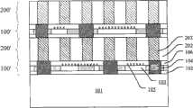
采用根据第一实施例和第二实施例的堆叠方法,最终形成了相同结构的堆叠的半导体器件10,如图10所示。该半导体器件10包括半导体衬底101,以及位于半导体衬底101上的多个层面的晶片组件。每一层面的晶片组件包括有源部件100’和键合部件200’,其中,在有源部件100’和键合部件200’中形成了对齐的贯穿导电通道107、203。每一个层面的有源部件100’利用贯穿导电通道107、203与下一层面/上一层面的有源部件100’电连接。Using the stacking methods according to the first embodiment and the second embodiment, a stacked semiconductor device 10 with the same structure is finally formed, as shown in FIG. 10 . The semiconductor device 10 includes a
在该半导体器件10中,即使有源部件100’的厚度很薄,由于键合部件200’的支撑作用,也不会在图4和图5所示的化学机械平面化和转移步骤中破裂。而且,由于可以使用厚度减小的有源部件100’,因此可以相应地显著减小贯穿导电通道107的深宽比,使得刻蚀容易完全进行并且节省了刻蚀时间。In this semiconductor device 10, even if the thickness of the active part 100' is thin, there is no cracking in the chemical mechanical planarization and transfer steps shown in FIGS. 4 and 5 due to the supporting function of the bonding part 200'. Moreover, since the active component 100' with reduced thickness can be used, the aspect ratio of the through conductive via 107 can be correspondingly significantly reduced, so that the etching can be easily performed completely and the etching time can be saved.
以上描述只是为了示例说明和描述本发明,而非意图穷举和限制本发明。因此,本发明不局限于所描述的实施例。对于本领域的技术人员明显可知的变型或更改,均在本发明的保护范围之内。The above description is only for illustration and description of the present invention, not intended to be exhaustive and limitative of the present invention. Accordingly, the invention is not limited to the described embodiments. Variations or changes that are obvious to those skilled in the art are within the protection scope of the present invention.
Claims (10)
Translated fromChinesePriority Applications (3)
| Application Number | Priority Date | Filing Date | Title |
|---|---|---|---|
| CN201010540727.0ACN102468284B (en) | 2010-11-10 | 2010-11-10 | Stacked semiconductor device and manufacturing method thereof |
| US13/120,792US8557677B2 (en) | 2010-11-10 | 2011-02-17 | Stack-type semiconductor device and method for manufacturing the same |
| PCT/CN2011/071057WO2012062060A1 (en) | 2010-11-10 | 2011-02-17 | Stacked semiconductor device and manufacturing method thereof |
Applications Claiming Priority (1)
| Application Number | Priority Date | Filing Date | Title |
|---|---|---|---|
| CN201010540727.0ACN102468284B (en) | 2010-11-10 | 2010-11-10 | Stacked semiconductor device and manufacturing method thereof |
Publications (2)
| Publication Number | Publication Date |
|---|---|
| CN102468284Atrue CN102468284A (en) | 2012-05-23 |
| CN102468284B CN102468284B (en) | 2014-04-16 |
Family
ID=46050350
Family Applications (1)
| Application Number | Title | Priority Date | Filing Date |
|---|---|---|---|
| CN201010540727.0AActiveCN102468284B (en) | 2010-11-10 | 2010-11-10 | Stacked semiconductor device and manufacturing method thereof |
Country Status (2)
| Country | Link |
|---|---|
| CN (1) | CN102468284B (en) |
| WO (1) | WO2012062060A1 (en) |
Cited By (10)
| Publication number | Priority date | Publication date | Assignee | Title |
|---|---|---|---|---|
| WO2014040360A1 (en)* | 2012-09-17 | 2014-03-20 | 江苏物联网研究发展中心 | High-voltage super-junction igbt manufacturing method |
| CN109994444A (en)* | 2019-03-29 | 2019-07-09 | 长江存储科技有限责任公司 | Wafer bonding structure and fabrication method thereof |
| CN110137134A (en)* | 2019-05-05 | 2019-08-16 | 中国科学院微电子研究所 | Interconnect structures, circuits, and electronic equipment including the interconnect structures or circuits |
| CN110676246A (en)* | 2018-07-02 | 2020-01-10 | 台湾积体电路制造股份有限公司 | Integrated chip |
| CN111180425A (en)* | 2018-11-09 | 2020-05-19 | 南亚科技股份有限公司 | Method and system for manufacturing stacked wafer |
| US20200176466A1 (en)* | 2018-11-30 | 2020-06-04 | Yangtze Memory Technologies Co., Ltd. | Bonded memory device and fabrication methods thereof |
| CN111383992A (en)* | 2020-03-23 | 2020-07-07 | 长江存储科技有限责任公司 | Manufacturing method of semiconductor device |
| US10770434B2 (en) | 2016-09-30 | 2020-09-08 | Intel Corporation | Stair-stacked dice device in a system in package, and methods of making same |
| CN114759130A (en)* | 2022-06-15 | 2022-07-15 | 镭昱光电科技(苏州)有限公司 | Micro-LED display chip and preparation method thereof |
| CN116072607A (en)* | 2023-03-07 | 2023-05-05 | 湖北江城实验室 | Package structure, forming method thereof and electronic equipment |
Families Citing this family (1)
| Publication number | Priority date | Publication date | Assignee | Title |
|---|---|---|---|---|
| CN119176521B (en)* | 2024-11-25 | 2025-08-05 | 烟台齐新半导体技术研究院有限公司 | A method for preparing a hollow structure in a semiconductor device |
Citations (3)
| Publication number | Priority date | Publication date | Assignee | Title |
|---|---|---|---|---|
| US20100032795A1 (en)* | 2008-08-06 | 2010-02-11 | Aitken John M | Design structure for semiconductor device having radiation hardened insulators and structure thereof |
| US20100182041A1 (en)* | 2009-01-22 | 2010-07-22 | International Business Machines Corporation | 3d chip-stack with fuse-type through silicon via |
| US20100264551A1 (en)* | 2009-04-20 | 2010-10-21 | International Business Machines Corporation | Three dimensional integrated circuit integration using dielectric bonding first and through via formation last |
Family Cites Families (3)
| Publication number | Priority date | Publication date | Assignee | Title |
|---|---|---|---|---|
| CN100517623C (en)* | 2006-12-05 | 2009-07-22 | 中芯国际集成电路制造(上海)有限公司 | Chip bonding method and its structure |
| US8647923B2 (en)* | 2009-04-06 | 2014-02-11 | Canon Kabushiki Kaisha | Method of manufacturing semiconductor device |
| CN101834152B (en)* | 2010-04-20 | 2012-08-22 | 中国科学院上海微系统与信息技术研究所 | Method for manufacturing three-dimensionally stacked resistance conversion memory |
- 2010
- 2010-11-10CNCN201010540727.0Apatent/CN102468284B/enactiveActive
- 2011
- 2011-02-17WOPCT/CN2011/071057patent/WO2012062060A1/enactiveApplication Filing
Patent Citations (3)
| Publication number | Priority date | Publication date | Assignee | Title |
|---|---|---|---|---|
| US20100032795A1 (en)* | 2008-08-06 | 2010-02-11 | Aitken John M | Design structure for semiconductor device having radiation hardened insulators and structure thereof |
| US20100182041A1 (en)* | 2009-01-22 | 2010-07-22 | International Business Machines Corporation | 3d chip-stack with fuse-type through silicon via |
| US20100264551A1 (en)* | 2009-04-20 | 2010-10-21 | International Business Machines Corporation | Three dimensional integrated circuit integration using dielectric bonding first and through via formation last |
Cited By (19)
| Publication number | Priority date | Publication date | Assignee | Title |
|---|---|---|---|---|
| WO2014040360A1 (en)* | 2012-09-17 | 2014-03-20 | 江苏物联网研究发展中心 | High-voltage super-junction igbt manufacturing method |
| CN103681321A (en)* | 2012-09-17 | 2014-03-26 | 中国科学院微电子研究所 | Manufacturing method of high-voltage super-junction IGBT |
| CN103681321B (en)* | 2012-09-17 | 2016-05-18 | 中国科学院微电子研究所 | Manufacturing method of high-voltage super-junction IGBT |
| US10770434B2 (en) | 2016-09-30 | 2020-09-08 | Intel Corporation | Stair-stacked dice device in a system in package, and methods of making same |
| CN110676246B (en)* | 2018-07-02 | 2024-11-12 | 台湾积体电路制造股份有限公司 | Integrated Chip |
| CN110676246A (en)* | 2018-07-02 | 2020-01-10 | 台湾积体电路制造股份有限公司 | Integrated chip |
| CN111180425A (en)* | 2018-11-09 | 2020-05-19 | 南亚科技股份有限公司 | Method and system for manufacturing stacked wafer |
| US12232316B2 (en) | 2018-11-30 | 2025-02-18 | Yangtze Memory Technologies Co., Ltd. | Bonded memory device and fabrication methods thereof |
| US20200176466A1 (en)* | 2018-11-30 | 2020-06-04 | Yangtze Memory Technologies Co., Ltd. | Bonded memory device and fabrication methods thereof |
| WO2020107452A1 (en)* | 2018-11-30 | 2020-06-04 | Yangtze Memory Technologies Co., Ltd. | Bonded memory device and fabrication methods thereof |
| US11114453B2 (en) | 2018-11-30 | 2021-09-07 | Yangtze Memory Technologies Co., Ltd. | Bonded memory device and fabrication methods thereof |
| CN109994444B (en)* | 2019-03-29 | 2021-07-16 | 长江存储科技有限责任公司 | Wafer bonding structure and fabrication method thereof |
| CN109994444A (en)* | 2019-03-29 | 2019-07-09 | 长江存储科技有限责任公司 | Wafer bonding structure and fabrication method thereof |
| CN110137134B (en)* | 2019-05-05 | 2021-02-09 | 中国科学院微电子研究所 | Interconnect structure, circuit and electronic device including the same |
| CN110137134A (en)* | 2019-05-05 | 2019-08-16 | 中国科学院微电子研究所 | Interconnect structures, circuits, and electronic equipment including the interconnect structures or circuits |
| US12199031B2 (en) | 2019-05-05 | 2025-01-14 | Institute of Microelectronics, Chinese Academy of Sciences | Interconnection structure, circuit and electronic apparatus including the interconnection structure or circuit |
| CN111383992A (en)* | 2020-03-23 | 2020-07-07 | 长江存储科技有限责任公司 | Manufacturing method of semiconductor device |
| CN114759130A (en)* | 2022-06-15 | 2022-07-15 | 镭昱光电科技(苏州)有限公司 | Micro-LED display chip and preparation method thereof |
| CN116072607A (en)* | 2023-03-07 | 2023-05-05 | 湖北江城实验室 | Package structure, forming method thereof and electronic equipment |
Also Published As
| Publication number | Publication date |
|---|---|
| CN102468284B (en) | 2014-04-16 |
| WO2012062060A1 (en) | 2012-05-18 |
Similar Documents
| Publication | Publication Date | Title |
|---|---|---|
| US11664349B2 (en) | Stacked chip package and methods of manufacture thereof | |
| CN102468284A (en) | Stacked semiconductor device and manufacturing method thereof | |
| US8519515B2 (en) | TSV structure and method for forming the same | |
| US20190115314A1 (en) | Methods and structures for wafer-level system in package | |
| US8283207B2 (en) | Methods for forming through-substrate conductor filled vias, and electronic assemblies formed using such methods | |
| US8168533B2 (en) | Through-silicon via structure and method for making the same | |
| CN102301465B (en) | Through-substrate vias | |
| US20130015504A1 (en) | Tsv structure and method for forming the same | |
| CN101847597B (en) | Integrated circuit structure | |
| TWI786535B (en) | Semiconductor device | |
| EP4187581A1 (en) | An interconnect structure of a semiconductor component and methods for producing said structure | |
| TWI822153B (en) | Package structure and method for forming the same | |
| US20130161825A1 (en) | Through substrate via structure and method for fabricating the same | |
| CN102263099B (en) | 3D integrated circuit and manufacturing method thereof | |
| CN104752378A (en) | Semiconductor devices and methods of manufacture thereof | |
| TW202147511A (en) | Integrated chip structure and method of forming the same | |
| CN113345857A (en) | Semiconductor element and method for manufacturing the same | |
| CN103515302B (en) | Semiconductor device and method of manufacture | |
| JP2016157832A (en) | Semiconductor device and manufacturing method of the same | |
| US10438887B2 (en) | Semiconductor chip and multi-chip package using thereof and method for manufacturing the same | |
| US7579258B2 (en) | Semiconductor interconnect having adjacent reservoir for bonding and method for formation | |
| US8557677B2 (en) | Stack-type semiconductor device and method for manufacturing the same | |
| US8822336B2 (en) | Through-silicon via forming method | |
| CN103456716B (en) | Three-dimensional multi-chip laminated module and manufacturing method thereof | |
| CN106057776A (en) | Electronic package that includes a plurality of integrated circuit devices bonded in a three-dimensional stack arrangement |
Legal Events
| Date | Code | Title | Description |
|---|---|---|---|
| C06 | Publication | ||
| PB01 | Publication | ||
| C10 | Entry into substantive examination | ||
| SE01 | Entry into force of request for substantive examination | ||
| C14 | Grant of patent or utility model | ||
| GR01 | Patent grant |