CN102460750A - Metal substrate and light source device - Google Patents
Metal substrate and light source deviceDownload PDFInfo
- Publication number
- CN102460750A CN102460750ACN2010800239845ACN201080023984ACN102460750ACN 102460750 ACN102460750 ACN 102460750ACN 2010800239845 ACN2010800239845 ACN 2010800239845ACN 201080023984 ACN201080023984 ACN 201080023984ACN 102460750 ACN102460750 ACN 102460750A
- Authority
- CN
- China
- Prior art keywords
- light source
- layer
- mounting surface
- metal substrate
- metal
- Prior art date
- Legal status (The legal status is an assumption and is not a legal conclusion. Google has not performed a legal analysis and makes no representation as to the accuracy of the status listed.)
- Pending
Links
- 229910052751metalInorganic materials0.000titleclaimsabstractdescription198
- 239000002184metalSubstances0.000titleclaimsabstractdescription198
- 239000000758substrateSubstances0.000titleclaimsabstractdescription152
- 229920005989resinPolymers0.000claimsabstractdescription91
- 239000011347resinSubstances0.000claimsabstractdescription91
- 239000004065semiconductorSubstances0.000claimsabstractdescription34
- 239000010409thin filmSubstances0.000claimsabstractdescription28
- 239000010408filmSubstances0.000claimsdescription123
- OAICVXFJPJFONN-UHFFFAOYSA-NPhosphorusChemical compound[P]OAICVXFJPJFONN-UHFFFAOYSA-N0.000claimsdescription78
- 238000007747platingMethods0.000claimsdescription22
- 239000000919ceramicSubstances0.000claimsdescription14
- 230000009467reductionEffects0.000claimsdescription8
- 239000000463materialSubstances0.000abstractdescription18
- 239000010410layerSubstances0.000description132
- 239000010931goldSubstances0.000description73
- PXHVJJICTQNCMI-UHFFFAOYSA-NnickelSubstances[Ni]PXHVJJICTQNCMI-UHFFFAOYSA-N0.000description52
- 238000000034methodMethods0.000description46
- 230000000052comparative effectEffects0.000description45
- RYGMFSIKBFXOCR-UHFFFAOYSA-NCopperChemical compound[Cu]RYGMFSIKBFXOCR-UHFFFAOYSA-N0.000description38
- 239000002585baseSubstances0.000description28
- 230000004907fluxEffects0.000description28
- 229910000679solderInorganic materials0.000description26
- 229920005992thermoplastic resinPolymers0.000description23
- 239000011342resin compositionSubstances0.000description22
- 239000004697PolyetherimideSubstances0.000description20
- 229920001601polyetherimidePolymers0.000description20
- 239000000945fillerSubstances0.000description19
- GWEVSGVZZGPLCZ-UHFFFAOYSA-NTitan oxideChemical compoundO=[Ti]=OGWEVSGVZZGPLCZ-UHFFFAOYSA-N0.000description18
- OGIDPMRJRNCKJF-UHFFFAOYSA-Ntitanium oxideInorganic materials[Ti]=OOGIDPMRJRNCKJF-UHFFFAOYSA-N0.000description18
- 239000011575calciumSubstances0.000description14
- 230000008569processEffects0.000description14
- 229910052782aluminiumInorganic materials0.000description12
- 229910052788bariumInorganic materials0.000description12
- 229910052791calciumInorganic materials0.000description12
- 239000010949copperSubstances0.000description12
- 230000007423decreaseEffects0.000description12
- 238000010438heat treatmentMethods0.000description12
- 230000008018meltingEffects0.000description12
- 238000002844meltingMethods0.000description12
- 229910052712strontiumInorganic materials0.000description12
- 239000013078crystalSubstances0.000description11
- 239000011256inorganic fillerSubstances0.000description11
- 229910003475inorganic fillerInorganic materials0.000description11
- 238000004519manufacturing processMethods0.000description11
- 239000002245particleSubstances0.000description11
- 239000011241protective layerSubstances0.000description11
- 239000011889copper foilSubstances0.000description10
- 238000000465mouldingMethods0.000description10
- 239000004696Poly ether ether ketoneSubstances0.000description9
- 229910052775ThuliumInorganic materials0.000description9
- 239000000203mixtureSubstances0.000description9
- 229920002530polyetherether ketonePolymers0.000description9
- XAGFODPZIPBFFR-UHFFFAOYSA-NaluminiumChemical compound[Al]XAGFODPZIPBFFR-UHFFFAOYSA-N0.000description8
- 239000011888foilSubstances0.000description7
- 229910052737goldInorganic materials0.000description7
- 238000005259measurementMethods0.000description7
- 229920001187thermosetting polymerPolymers0.000description7
- XLOMVQKBTHCTTD-UHFFFAOYSA-NZinc monoxideChemical compound[Zn]=OXLOMVQKBTHCTTD-UHFFFAOYSA-N0.000description6
- 238000005266castingMethods0.000description6
- 238000007772electroless platingMethods0.000description6
- 230000009477glass transitionEffects0.000description6
- 230000017525heat dissipationEffects0.000description6
- 229910052749magnesiumInorganic materials0.000description6
- 239000011777magnesiumSubstances0.000description6
- 238000009877renderingMethods0.000description6
- 229920002050silicone resinPolymers0.000description6
- 239000000460chlorineSubstances0.000description5
- 238000002425crystallisationMethods0.000description5
- 230000000694effectsEffects0.000description5
- 238000011156evaluationMethods0.000description5
- 238000001125extrusionMethods0.000description5
- 238000010030laminatingMethods0.000description5
- VTYYLEPIZMXCLO-UHFFFAOYSA-LCalcium carbonateChemical compound[Ca+2].[O-]C([O-])=OVTYYLEPIZMXCLO-UHFFFAOYSA-L0.000description4
- 229920000106Liquid crystal polymerPolymers0.000description4
- 239000004977Liquid-crystal polymers (LCPs)Substances0.000description4
- 239000004734Polyphenylene sulfideSubstances0.000description4
- VYPSYNLAJGMNEJ-UHFFFAOYSA-NSilicium dioxideChemical compoundO=[Si]=OVYPSYNLAJGMNEJ-UHFFFAOYSA-N0.000description4
- RTAQQCXQSZGOHL-UHFFFAOYSA-NTitaniumChemical compound[Ti]RTAQQCXQSZGOHL-UHFFFAOYSA-N0.000description4
- PNEYBMLMFCGWSK-UHFFFAOYSA-Naluminium oxideInorganic materials[O-2].[O-2].[O-2].[Al+3].[Al+3]PNEYBMLMFCGWSK-UHFFFAOYSA-N0.000description4
- TZCXTZWJZNENPQ-UHFFFAOYSA-Lbarium sulfateChemical compound[Ba+2].[O-]S([O-])(=O)=OTZCXTZWJZNENPQ-UHFFFAOYSA-L0.000description4
- 230000008859changeEffects0.000description4
- 238000006243chemical reactionMethods0.000description4
- 239000003822epoxy resinSubstances0.000description4
- 239000004973liquid crystal related substanceSubstances0.000description4
- 238000002156mixingMethods0.000description4
- 229920000647polyepoxidePolymers0.000description4
- 229920000069polyphenylene sulfidePolymers0.000description4
- 238000002360preparation methodMethods0.000description4
- 238000004080punchingMethods0.000description4
- 238000012360testing methodMethods0.000description4
- 229910015363Au—SnInorganic materials0.000description3
- ZAMOUSCENKQFHK-UHFFFAOYSA-NChlorine atomChemical compound[Cl]ZAMOUSCENKQFHK-UHFFFAOYSA-N0.000description3
- 229910003564SiAlONInorganic materials0.000description3
- 229910004283SiO 4Inorganic materials0.000description3
- 239000006087Silane Coupling AgentSubstances0.000description3
- BQCADISMDOOEFD-UHFFFAOYSA-NSilverChemical compound[Ag]BQCADISMDOOEFD-UHFFFAOYSA-N0.000description3
- RJDOZRNNYVAULJ-UHFFFAOYSA-L[O--].[O--].[O--].[O--].[O--].[O--].[O--].[O--].[O--].[O--].[F-].[F-].[Mg++].[Mg++].[Mg++].[Al+3].[Si+4].[Si+4].[Si+4].[K+]Chemical compound[O--].[O--].[O--].[O--].[O--].[O--].[O--].[O--].[O--].[O--].[F-].[F-].[Mg++].[Mg++].[Mg++].[Al+3].[Si+4].[Si+4].[Si+4].[K+]RJDOZRNNYVAULJ-UHFFFAOYSA-L0.000description3
- 239000000654additiveSubstances0.000description3
- 230000015572biosynthetic processEffects0.000description3
- 229910019990cerium-doped yttrium aluminum garnetInorganic materials0.000description3
- 229910052801chlorineInorganic materials0.000description3
- 230000005284excitationEffects0.000description3
- 239000011521glassSubstances0.000description3
- 229910052809inorganic oxideInorganic materials0.000description3
- 238000003475laminationMethods0.000description3
- 239000010445micaSubstances0.000description3
- 229910052618mica groupInorganic materials0.000description3
- 229920002312polyamide-imidePolymers0.000description3
- 238000003825pressingMethods0.000description3
- 238000012545processingMethods0.000description3
- 238000002310reflectometryMethods0.000description3
- 229910052709silverInorganic materials0.000description3
- 239000004332silverSubstances0.000description3
- 238000006467substitution reactionMethods0.000description3
- 239000010936titaniumSubstances0.000description3
- 230000007704transitionEffects0.000description3
- 239000011787zinc oxideSubstances0.000description3
- 102100032047AlsinHuman genes0.000description2
- 101710187109AlsinProteins0.000description2
- 229910052684CeriumInorganic materials0.000description2
- JMASRVWKEDWRBT-UHFFFAOYSA-NGallium nitrideChemical compound[Ga]#NJMASRVWKEDWRBT-UHFFFAOYSA-N0.000description2
- 239000004594Masterbatch (MB)Substances0.000description2
- 229920008285Poly(ether ketone) PEKPolymers0.000description2
- 239000004962Polyamide-imideSubstances0.000description2
- QAOWNCQODCNURD-UHFFFAOYSA-NSulfuric acidChemical compoundOS(O)(=O)=OQAOWNCQODCNURD-UHFFFAOYSA-N0.000description2
- HCHKCACWOHOZIP-UHFFFAOYSA-NZincChemical group[Zn]HCHKCACWOHOZIP-UHFFFAOYSA-N0.000description2
- MCMNRKCIXSYSNV-UHFFFAOYSA-NZirconium dioxideChemical compoundO=[Zr]=OMCMNRKCIXSYSNV-UHFFFAOYSA-N0.000description2
- 238000005275alloyingMethods0.000description2
- 229910000019calcium carbonateInorganic materials0.000description2
- 239000011248coating agentSubstances0.000description2
- 238000000576coating methodMethods0.000description2
- 230000008025crystallizationEffects0.000description2
- 230000006866deteriorationEffects0.000description2
- 238000009792diffusion processMethods0.000description2
- ZUOUZKKEUPVFJK-UHFFFAOYSA-NdiphenylChemical groupC1=CC=CC=C1C1=CC=CC=C1ZUOUZKKEUPVFJK-UHFFFAOYSA-N0.000description2
- 238000001035dryingMethods0.000description2
- 238000005516engineering processMethods0.000description2
- PCHJSUWPFVWCPO-UHFFFAOYSA-NgoldChemical compound[Au]PCHJSUWPFVWCPO-UHFFFAOYSA-N0.000description2
- NLYAJNPCOHFWQQ-UHFFFAOYSA-NkaolinChemical compoundO.O.O=[Al]O[Si](=O)O[Si](=O)O[Al]=ONLYAJNPCOHFWQQ-UHFFFAOYSA-N0.000description2
- 229910052746lanthanumInorganic materials0.000description2
- 238000004020luminiscence typeMethods0.000description2
- 238000001579optical reflectometryMethods0.000description2
- 230000000704physical effectEffects0.000description2
- 229920001721polyimidePolymers0.000description2
- 239000009719polyimide resinSubstances0.000description2
- 229920001955polyphenylene etherPolymers0.000description2
- 229920012287polyphenylene sulfonePolymers0.000description2
- 230000005855radiationEffects0.000description2
- 230000004044responseEffects0.000description2
- 229910052710siliconInorganic materials0.000description2
- 239000000377silicon dioxideSubstances0.000description2
- 239000000126substanceSubstances0.000description2
- 239000000454talcSubstances0.000description2
- 229910052623talcInorganic materials0.000description2
- 229910052719titaniumInorganic materials0.000description2
- 239000012463white pigmentSubstances0.000description2
- 229910052725zincInorganic materials0.000description2
- 239000011701zincSubstances0.000description2
- WZCQRUWWHSTZEM-UHFFFAOYSA-N1,3-phenylenediamineChemical compoundNC1=CC=CC(N)=C1WZCQRUWWHSTZEM-UHFFFAOYSA-N0.000description1
- CBCKQZAAMUWICA-UHFFFAOYSA-N1,4-phenylenediamineChemical compoundNC1=CC=C(N)C=C1CBCKQZAAMUWICA-UHFFFAOYSA-N0.000description1
- KXGFMDJXCMQABM-UHFFFAOYSA-N2-methoxy-6-methylphenolChemical compound[CH]OC1=CC=CC([CH])=C1OKXGFMDJXCMQABM-UHFFFAOYSA-N0.000description1
- 229920000178Acrylic resinPolymers0.000description1
- 239000004925Acrylic resinSubstances0.000description1
- 229910000980Aluminium gallium arsenideInorganic materials0.000description1
- 239000005995Aluminium silicateSubstances0.000description1
- 229910000789Aluminium-silicon alloyInorganic materials0.000description1
- PZNSFCLAULLKQX-UHFFFAOYSA-NBoron nitrideChemical compoundN#BPZNSFCLAULLKQX-UHFFFAOYSA-N0.000description1
- 241001391944Commicarpus scandensSpecies0.000description1
- 229910020068MgAlInorganic materials0.000description1
- GRYLNZFGIOXLOG-UHFFFAOYSA-NNitric acidChemical compoundO[N+]([O-])=OGRYLNZFGIOXLOG-UHFFFAOYSA-N0.000description1
- 229920012266Poly(ether sulfone) PESPolymers0.000description1
- 229910052771TerbiumInorganic materials0.000description1
- ATJFFYVFTNAWJD-UHFFFAOYSA-NTinChemical compound[Sn]ATJFFYVFTNAWJD-UHFFFAOYSA-N0.000description1
- 229920004747ULTEM® 1000Polymers0.000description1
- 229920004748ULTEM® 1010Polymers0.000description1
- 229920004813ULTEM® CRS5001Polymers0.000description1
- 229920004846ULTEM® UF5011SPolymers0.000description1
- 229920004695VICTREX™ PEEKPolymers0.000description1
- 239000005083Zinc sulfideSubstances0.000description1
- 239000006096absorbing agentSubstances0.000description1
- 238000010521absorption reactionMethods0.000description1
- 239000002253acidSubstances0.000description1
- 239000000853adhesiveSubstances0.000description1
- 230000001070adhesive effectEffects0.000description1
- 239000012790adhesive layerSubstances0.000description1
- 239000003513alkaliSubstances0.000description1
- WNROFYMDJYEPJX-UHFFFAOYSA-Kaluminium hydroxideChemical compound[OH-].[OH-].[OH-].[Al+3]WNROFYMDJYEPJX-UHFFFAOYSA-K0.000description1
- 235000012211aluminium silicateNutrition0.000description1
- 150000008064anhydridesChemical class0.000description1
- 229910000410antimony oxideInorganic materials0.000description1
- 230000004888barrier functionEffects0.000description1
- 239000011230binding agentSubstances0.000description1
- 230000005540biological transmissionEffects0.000description1
- 235000010290biphenylNutrition0.000description1
- 239000004305biphenylSubstances0.000description1
- 229910001593boehmiteInorganic materials0.000description1
- 229910052804chromiumInorganic materials0.000description1
- 239000004927claySubstances0.000description1
- 229910052570clayInorganic materials0.000description1
- 239000003086colorantSubstances0.000description1
- 238000004040coloringMethods0.000description1
- 239000002131composite materialSubstances0.000description1
- 230000008602contractionEffects0.000description1
- 229910052802copperInorganic materials0.000description1
- 229920006038crystalline resinPolymers0.000description1
- 238000001723curingMethods0.000description1
- 238000007766curtain coatingMethods0.000description1
- 238000005520cutting processMethods0.000description1
- GUJOJGAPFQRJSV-UHFFFAOYSA-Ndialuminum;dioxosilane;oxygen(2-);hydrateChemical compoundO.[O-2].[O-2].[O-2].[Al+3].[Al+3].O=[Si]=O.O=[Si]=O.O=[Si]=O.O=[Si]=OGUJOJGAPFQRJSV-UHFFFAOYSA-N0.000description1
- NKZSPGSOXYXWQA-UHFFFAOYSA-Ndioxido(oxo)titanium;lead(2+)Chemical compound[Pb+2].[O-][Ti]([O-])=ONKZSPGSOXYXWQA-UHFFFAOYSA-N0.000description1
- NJLLQSBAHIKGKF-UHFFFAOYSA-Ndipotassium dioxido(oxo)titaniumChemical compound[K+].[K+].[O-][Ti]([O-])=ONJLLQSBAHIKGKF-UHFFFAOYSA-N0.000description1
- YGANSGVIUGARFR-UHFFFAOYSA-Ndipotassium dioxosilane oxo(oxoalumanyloxy)alumane oxygen(2-)Chemical compound[O--].[K+].[K+].O=[Si]=O.O=[Al]O[Al]=OYGANSGVIUGARFR-UHFFFAOYSA-N0.000description1
- 238000002845discolorationMethods0.000description1
- 238000005553drillingMethods0.000description1
- 239000008393encapsulating agentSubstances0.000description1
- 238000012053enzymatic serum creatinine assayMethods0.000description1
- RTZKZFJDLAIYFH-UHFFFAOYSA-NetherSubstancesCCOCCRTZKZFJDLAIYFH-UHFFFAOYSA-N0.000description1
- 230000005496eutecticsEffects0.000description1
- 238000011049fillingMethods0.000description1
- 239000003063flame retardantSubstances0.000description1
- 238000013007heat curingMethods0.000description1
- 230000020169heat generationEffects0.000description1
- 239000012760heat stabilizerSubstances0.000description1
- FAHBNUUHRFUEAI-UHFFFAOYSA-MhydroxidooxidoaluminiumChemical compoundO[Al]=OFAHBNUUHRFUEAI-UHFFFAOYSA-M0.000description1
- 229910052900illiteInorganic materials0.000description1
- 238000005286illuminationMethods0.000description1
- 230000001771impaired effectEffects0.000description1
- 238000009413insulationMethods0.000description1
- 125000000654isopropylidene groupChemical groupC(C)(C)=*0.000description1
- 229910052622kaoliniteInorganic materials0.000description1
- 150000002576ketonesChemical class0.000description1
- 239000000314lubricantSubstances0.000description1
- 229940018564m-phenylenediamineDrugs0.000description1
- 239000000395magnesium oxideSubstances0.000description1
- CPLXHLVBOLITMK-UHFFFAOYSA-Nmagnesium oxideInorganic materials[Mg]=OCPLXHLVBOLITMK-UHFFFAOYSA-N0.000description1
- AXZKOIWUVFPNLO-UHFFFAOYSA-Nmagnesium;oxygen(2-)Chemical compound[O-2].[Mg+2]AXZKOIWUVFPNLO-UHFFFAOYSA-N0.000description1
- 229910052748manganeseInorganic materials0.000description1
- 229910052901montmorilloniteInorganic materials0.000description1
- 229910052627muscoviteInorganic materials0.000description1
- 229910052759nickelInorganic materials0.000description1
- 229910017604nitric acidInorganic materials0.000description1
- VGIBGUSAECPPNB-UHFFFAOYSA-Lnonaaluminum;magnesium;tripotassium;1,3-dioxido-2,4,5-trioxa-1,3-disilabicyclo[1.1.1]pentane;iron(2+);oxygen(2-);fluoride;hydroxideChemical compound[OH-].[O-2].[O-2].[O-2].[O-2].[O-2].[F-].[Mg+2].[Al+3].[Al+3].[Al+3].[Al+3].[Al+3].[Al+3].[Al+3].[Al+3].[Al+3].[K+].[K+].[K+].[Fe+2].O1[Si]2([O-])O[Si]1([O-])O2.O1[Si]2([O-])O[Si]1([O-])O2.O1[Si]2([O-])O[Si]1([O-])O2.O1[Si]2([O-])O[Si]1([O-])O2.O1[Si]2([O-])O[Si]1([O-])O2.O1[Si]2([O-])O[Si]1([O-])O2.O1[Si]2([O-])O[Si]1([O-])O2VGIBGUSAECPPNB-UHFFFAOYSA-L0.000description1
- 239000002667nucleating agentSubstances0.000description1
- 238000007500overflow downdraw methodMethods0.000description1
- 238000010525oxidative degradation reactionMethods0.000description1
- TWNQGVIAIRXVLR-UHFFFAOYSA-Noxo(oxoalumanyloxy)alumaneChemical compoundO=[Al]O[Al]=OTWNQGVIAIRXVLR-UHFFFAOYSA-N0.000description1
- VTRUBDSFZJNXHI-UHFFFAOYSA-NoxoantimonyChemical compound[Sb]=OVTRUBDSFZJNXHI-UHFFFAOYSA-N0.000description1
- RVTZCBVAJQQJTK-UHFFFAOYSA-Noxygen(2-);zirconium(4+)Chemical compound[O-2].[O-2].[Zr+4]RVTZCBVAJQQJTK-UHFFFAOYSA-N0.000description1
- 239000005022packaging materialSubstances0.000description1
- 229920001568phenolic resinPolymers0.000description1
- 239000005011phenolic resinSubstances0.000description1
- 229910052628phlogopiteInorganic materials0.000description1
- 230000001699photocatalysisEffects0.000description1
- -1photostabilizersSubstances0.000description1
- 239000000049pigmentSubstances0.000description1
- 238000009832plasma treatmentMethods0.000description1
- 229920001643poly(ether ketone)Polymers0.000description1
- 229920001296polysiloxanePolymers0.000description1
- 238000004382pottingMethods0.000description1
- 239000000843powderSubstances0.000description1
- 238000011160researchMethods0.000description1
- 238000005096rolling processMethods0.000description1
- SBIBMFFZSBJNJF-UHFFFAOYSA-Nselenium;zincChemical compound[Se]=[Zn]SBIBMFFZSBJNJF-UHFFFAOYSA-N0.000description1
- 235000012239silicon dioxideNutrition0.000description1
- 229910021647smectiteInorganic materials0.000description1
- 238000005476solderingMethods0.000description1
- 238000004544sputter depositionMethods0.000description1
- 125000000472sulfonyl groupChemical group*S(*)(=O)=O0.000description1
- 238000004381surface treatmentMethods0.000description1
- 230000008646thermal stressEffects0.000description1
- 229910052718tinInorganic materials0.000description1
- 238000001771vacuum depositionMethods0.000description1
- 238000007740vapor depositionMethods0.000description1
- 229910052902vermiculiteInorganic materials0.000description1
- 239000010455vermiculiteSubstances0.000description1
- 235000019354vermiculiteNutrition0.000description1
- XLYOFNOQVPJJNP-UHFFFAOYSA-NwaterSubstancesOXLYOFNOQVPJJNP-UHFFFAOYSA-N0.000description1
- 238000003466weldingMethods0.000description1
- 238000004383yellowingMethods0.000description1
- 229910052727yttriumInorganic materials0.000description1
- 229910052984zinc sulfideInorganic materials0.000description1
- DRDVZXDWVBGGMH-UHFFFAOYSA-Nzinc;sulfideChemical compound[S-2].[Zn+2]DRDVZXDWVBGGMH-UHFFFAOYSA-N0.000description1
- 229910001928zirconium oxideInorganic materials0.000description1
Images


Classifications
- H—ELECTRICITY
- H10—SEMICONDUCTOR DEVICES; ELECTRIC SOLID-STATE DEVICES NOT OTHERWISE PROVIDED FOR
- H10H—INORGANIC LIGHT-EMITTING SEMICONDUCTOR DEVICES HAVING POTENTIAL BARRIERS
- H10H20/00—Individual inorganic light-emitting semiconductor devices having potential barriers, e.g. light-emitting diodes [LED]
- H10H20/80—Constructional details
- H10H20/85—Packages
- H10H20/858—Means for heat extraction or cooling
- H10H20/8581—Means for heat extraction or cooling characterised by their material
- H—ELECTRICITY
- H01—ELECTRIC ELEMENTS
- H01L—SEMICONDUCTOR DEVICES NOT COVERED BY CLASS H10
- H01L2224/00—Indexing scheme for arrangements for connecting or disconnecting semiconductor or solid-state bodies and methods related thereto as covered by H01L24/00
- H01L2224/01—Means for bonding being attached to, or being formed on, the surface to be connected, e.g. chip-to-package, die-attach, "first-level" interconnects; Manufacturing methods related thereto
- H01L2224/26—Layer connectors, e.g. plate connectors, solder or adhesive layers; Manufacturing methods related thereto
- H01L2224/2612—Auxiliary members for layer connectors, e.g. spacers
- H—ELECTRICITY
- H01—ELECTRIC ELEMENTS
- H01L—SEMICONDUCTOR DEVICES NOT COVERED BY CLASS H10
- H01L2224/00—Indexing scheme for arrangements for connecting or disconnecting semiconductor or solid-state bodies and methods related thereto as covered by H01L24/00
- H01L2224/01—Means for bonding being attached to, or being formed on, the surface to be connected, e.g. chip-to-package, die-attach, "first-level" interconnects; Manufacturing methods related thereto
- H01L2224/42—Wire connectors; Manufacturing methods related thereto
- H01L2224/47—Structure, shape, material or disposition of the wire connectors after the connecting process
- H01L2224/48—Structure, shape, material or disposition of the wire connectors after the connecting process of an individual wire connector
- H01L2224/4805—Shape
- H01L2224/4809—Loop shape
- H01L2224/48091—Arched
- H—ELECTRICITY
- H01—ELECTRIC ELEMENTS
- H01L—SEMICONDUCTOR DEVICES NOT COVERED BY CLASS H10
- H01L2224/00—Indexing scheme for arrangements for connecting or disconnecting semiconductor or solid-state bodies and methods related thereto as covered by H01L24/00
- H01L2224/01—Means for bonding being attached to, or being formed on, the surface to be connected, e.g. chip-to-package, die-attach, "first-level" interconnects; Manufacturing methods related thereto
- H01L2224/42—Wire connectors; Manufacturing methods related thereto
- H01L2224/47—Structure, shape, material or disposition of the wire connectors after the connecting process
- H01L2224/48—Structure, shape, material or disposition of the wire connectors after the connecting process of an individual wire connector
- H01L2224/481—Disposition
- H01L2224/48151—Connecting between a semiconductor or solid-state body and an item not being a semiconductor or solid-state body, e.g. chip-to-substrate, chip-to-passive
- H01L2224/48221—Connecting between a semiconductor or solid-state body and an item not being a semiconductor or solid-state body, e.g. chip-to-substrate, chip-to-passive the body and the item being stacked
- H01L2224/48225—Connecting between a semiconductor or solid-state body and an item not being a semiconductor or solid-state body, e.g. chip-to-substrate, chip-to-passive the body and the item being stacked the item being non-metallic, e.g. insulating substrate with or without metallisation
- H01L2224/48227—Connecting between a semiconductor or solid-state body and an item not being a semiconductor or solid-state body, e.g. chip-to-substrate, chip-to-passive the body and the item being stacked the item being non-metallic, e.g. insulating substrate with or without metallisation connecting the wire to a bond pad of the item
- H—ELECTRICITY
- H01—ELECTRIC ELEMENTS
- H01L—SEMICONDUCTOR DEVICES NOT COVERED BY CLASS H10
- H01L2224/00—Indexing scheme for arrangements for connecting or disconnecting semiconductor or solid-state bodies and methods related thereto as covered by H01L24/00
- H01L2224/73—Means for bonding being of different types provided for in two or more of groups H01L2224/10, H01L2224/18, H01L2224/26, H01L2224/34, H01L2224/42, H01L2224/50, H01L2224/63, H01L2224/71
- H01L2224/732—Location after the connecting process
- H01L2224/73251—Location after the connecting process on different surfaces
- H01L2224/73265—Layer and wire connectors
- H—ELECTRICITY
- H01—ELECTRIC ELEMENTS
- H01L—SEMICONDUCTOR DEVICES NOT COVERED BY CLASS H10
- H01L23/00—Details of semiconductor or other solid state devices
- H01L23/12—Mountings, e.g. non-detachable insulating substrates
- H01L23/14—Mountings, e.g. non-detachable insulating substrates characterised by the material or its electrical properties
- H01L23/142—Metallic substrates having insulating layers
- H—ELECTRICITY
- H01—ELECTRIC ELEMENTS
- H01L—SEMICONDUCTOR DEVICES NOT COVERED BY CLASS H10
- H01L2924/00—Indexing scheme for arrangements or methods for connecting or disconnecting semiconductor or solid-state bodies as covered by H01L24/00
- H01L2924/013—Alloys
- H01L2924/0132—Binary Alloys
- H01L2924/01322—Eutectic Alloys, i.e. obtained by a liquid transforming into two solid phases
- H—ELECTRICITY
- H01—ELECTRIC ELEMENTS
- H01L—SEMICONDUCTOR DEVICES NOT COVERED BY CLASS H10
- H01L2924/00—Indexing scheme for arrangements or methods for connecting or disconnecting semiconductor or solid-state bodies as covered by H01L24/00
- H01L2924/10—Details of semiconductor or other solid state devices to be connected
- H01L2924/102—Material of the semiconductor or solid state bodies
- H01L2924/1025—Semiconducting materials
- H01L2924/10251—Elemental semiconductors, i.e. Group IV
- H01L2924/10253—Silicon [Si]
- H—ELECTRICITY
- H01—ELECTRIC ELEMENTS
- H01L—SEMICONDUCTOR DEVICES NOT COVERED BY CLASS H10
- H01L2924/00—Indexing scheme for arrangements or methods for connecting or disconnecting semiconductor or solid-state bodies as covered by H01L24/00
- H01L2924/15—Details of package parts other than the semiconductor or other solid state devices to be connected
- H01L2924/181—Encapsulation
- H—ELECTRICITY
- H01—ELECTRIC ELEMENTS
- H01L—SEMICONDUCTOR DEVICES NOT COVERED BY CLASS H10
- H01L2924/00—Indexing scheme for arrangements or methods for connecting or disconnecting semiconductor or solid-state bodies as covered by H01L24/00
- H01L2924/19—Details of hybrid assemblies other than the semiconductor or other solid state devices to be connected
- H01L2924/191—Disposition
- H01L2924/19101—Disposition of discrete passive components
- H01L2924/19107—Disposition of discrete passive components off-chip wires
- H—ELECTRICITY
- H10—SEMICONDUCTOR DEVICES; ELECTRIC SOLID-STATE DEVICES NOT OTHERWISE PROVIDED FOR
- H10H—INORGANIC LIGHT-EMITTING SEMICONDUCTOR DEVICES HAVING POTENTIAL BARRIERS
- H10H20/00—Individual inorganic light-emitting semiconductor devices having potential barriers, e.g. light-emitting diodes [LED]
- H10H20/80—Constructional details
- H10H20/85—Packages
- H10H20/857—Interconnections, e.g. lead-frames, bond wires or solder balls
Landscapes
- Led Device Packages (AREA)
- Cooling Or The Like Of Semiconductors Or Solid State Devices (AREA)
Abstract
Description
Translated fromChinese技术领域technical field
本发明涉及用于搭载作为光源的半导体芯片、特别是发光二极管芯片(以下也称为“LED芯片”)的金属基板以及使用该金属基板的光源装置,更详细地说,涉及可牢固地固定LED芯片、同时可使LED芯片所产生的热高效地散热的金属基板。The present invention relates to a metal substrate for mounting a semiconductor chip as a light source, especially a light-emitting diode chip (hereinafter also referred to as "LED chip") and a light source device using the metal substrate. More specifically, it relates to a Chips and metal substrates that efficiently dissipate heat generated by LED chips.
背景技术Background technique
作为二代光源受到关注的发光二极管(以下也称为“LED”)的用途已经从液晶背光源或汽车用灯确实地发展到照明领域全体。Light-emitting diodes (hereinafter, also referred to as "LEDs") that have attracted attention as second-generation light sources have steadily expanded from liquid crystal backlights and automotive lamps to the entire lighting field.
作为使用LED芯片的光源装置,有在由白色覆铜层合板制作的印刷布线基板上搭载LED芯片、然后用透明的有机硅树脂或环氧树脂进行树脂封装而制备的芯片型LED。还有通过嵌件成型将引线框埋入白色树脂反射器中制成复合封装体、在其用白色树脂反射器包围的引线框部上搭载LED芯片、在反射器内部填充封装树脂而制备的芯片型LED。这些芯片型LED焊装在电子仪器的主布线基板上。As a light source device using an LED chip, there is a chip-type LED prepared by mounting an LED chip on a printed wiring board made of a white copper-clad laminate, and then resin-encapsulating it with a transparent silicone resin or epoxy resin. There is also a chip prepared by embedding a lead frame in a white resin reflector to form a composite package by insert molding, mounting an LED chip on the lead frame surrounded by a white resin reflector, and filling the inside of the reflector with encapsulating resin. type LED. These chip-type LEDs are soldered on the main wiring board of electronic equipment.
在常规照明用途的LED光源装置中,大多是将多个高输出的LED芯片搭载在一个布线基板上,因此,使LED芯片所产生的热高效地散热、抑制表面温度的升高是很重要的。这是由于LED芯片的表面温度升高,则LED芯片的寿命或发光效率降低。对此,作为手段之一,提出了将LED芯片直接固定在主布线基板上的方式。而且,该主布线基板本身的放热特性也必须良好,因此人们对于绝缘金属基板的应用进行了广泛研究。绝缘金属基板具有以下结构:以填充有放热填料的热固化性树脂层作为绝缘层的布线基板层合在金属板上。但是,LED芯片搭载在绝缘树脂层上,因此放热特性不充分。In many LED light source devices for general lighting applications, many high-output LED chips are mounted on a single wiring board. Therefore, it is important to efficiently dissipate the heat generated by the LED chips and suppress the rise in surface temperature. . This is because when the surface temperature of the LED chip increases, the lifetime or luminous efficiency of the LED chip decreases. In response to this, as one of the means, a method of directly fixing the LED chip on the main wiring board has been proposed. Furthermore, the main wiring substrate itself must also have good heat dissipation characteristics, so extensive research has been conducted on the application of the insulated metal substrate. The insulated metal substrate has a structure in which a wiring substrate having a thermosetting resin layer filled with an exothermic filler as an insulating layer is laminated on a metal plate. However, since the LED chip is mounted on the insulating resin layer, heat dissipation characteristics are not sufficient.
因此,人们要求放热特性更为优异的LED芯片搭载用基板。与此要求相对应,在专利文献1和专利文献2,中提出了在LED芯片的搭载部位(凹腔底面)使金属板露出的金属基板。Therefore, there is a demand for a substrate for mounting an LED chip that is more excellent in heat dissipation characteristics. In response to this requirement,
现有技术文献prior art literature
专利文献patent documents
专利文献1:日本特开2006-339224号公报Patent Document 1: Japanese Patent Laid-Open No. 2006-339224
专利文献2:日本特开2008-235868号公报Patent Document 2: Japanese Patent Laid-Open No. 2008-235868
发明内容Contents of the invention
专利文献1的LED芯片搭载用基板中,可以将LED芯片直接搭载在金属板上。但是,在该文献所公开的LED光源装置中,LED芯片与金属板的接合使用导热性未必能说是良好的银浆。这是由于LED芯片搭载面是Al(铝)的表面,因此无法使用导热性高的焊料作为接合材料。In the LED chip mounting substrate of
另一方面,专利文献2中记载了:对Al板的表面进行镀Au(金)或镀Ag(银)的表面处理,在其上直接搭载LED芯片。可以使用焊料将LED芯片牢固地固定在镀Au层的表面。但是,虽然可以通过蒸镀法等干式工艺在Al板的表面镀Au,但是在Al和Au的界面,即使在常温下也发生剧烈的合金化反应,发生着色物质的生成以及物性的降低。着色物质的生成对于光源装置来讲是不优选的。On the other hand,
因此,本发明的主要课题是提供一种金属基板,该金属基板可使用金属接合材料将作为光源的半导体芯片牢固接合,并且可以通过金属板使所搭载的半导体芯片产生的热高效地散热。Therefore, a main object of the present invention is to provide a metal substrate capable of firmly bonding a semiconductor chip as a light source with a metal bonding material and efficiently dissipating heat generated by the mounted semiconductor chip through a metal plate.
此外,本发明的另一课题是提供一种光源装置,该光源装置通过金属基板将产生的热高效地散热,由此来抑制作为光源而搭载的半导体芯片表面温度的升高。Another object of the present invention is to provide a light source device that efficiently dissipates generated heat through a metal substrate, thereby suppressing an increase in the surface temperature of a semiconductor chip mounted as a light source.
本发明是为解决上述课题而完成的,以以下内容为主旨。The present invention has been made to solve the above-mentioned problems, and the gist of the invention is as follows.
根据第一发明,提供一种金属基板,其具有用于搭载作为光源的半导体芯片的光源搭载面,其特征在于:该金属基板具有由Au以外的金属形成的放热金属板、层合在该放热金属板上的一部分上的绝缘树脂制的白色薄膜、和层合在该放热金属板上的其他部分上的光源搭载面形成层,上述光源搭载面形成层是与上述放热金属板直接接触的金属层,上述光源搭载面是成为上述光源搭载面形成层的最表层的Au层的表面。According to the first invention, there is provided a metal substrate having a light source mounting surface for mounting a semiconductor chip as a light source, characterized in that the metal substrate has an exothermic metal plate formed of a metal other than Au, laminated on the A white film made of insulating resin on a part of the exothermic metal plate, and a light source mounting surface forming layer laminated on the other part of the exothermic metal plate, and the light source mounting surface forming layer is the same as that of the exothermic metal plate. The metal layer in direct contact with the light source mounting surface is the surface of the Au layer that is the outermost layer of the light source mounting surface forming layer.
在第一发明的金属基板中,优选白色薄膜在波长400nm~800nm范围的平均反射率为70%以上。In the metal substrate of the first invention, the white thin film preferably has an average reflectance of 70% or more in a wavelength range of 400 nm to 800 nm.
在第一发明的金属基板中,优选白色薄膜在260℃热处理5分钟后、在波长470nm下的反射率降低率为10%以下。In the metal substrate according to the first invention, it is preferable that the reduction rate of reflectance at a wavelength of 470 nm after the white thin film is heat-treated at 260° C. for 5 minutes is 10% or less.
在第一发明的金属基板中,白色薄膜可以具有MD(薄膜的移动方向)和TD(与移动方向正交的方向),这种情况下,优选MD的线性膨胀系数和TD的线性膨胀系数的平均值为35×10-6/℃以下。In the metal substrate of the first invention, the white thin film may have MD (moving direction of the thin film) and TD (direction perpendicular to the moving direction), and in this case, the linear expansion coefficient of MD and the linear expansion coefficient of TD are preferable. The average value is below 35×10-6 /°C.
在第一发明的金属基板中,优选白色薄膜具有贯通孔,在该贯通孔的位置形成光源搭载面形成层。In the metal substrate of the first invention, it is preferable that the white thin film has a through hole, and the light source mounting surface forming layer is formed at the position of the through hole.
在第一发明的金属基板中,优选上述光源搭载面形成层在成为最表层的Au层的正下方含有Ni层。In the metal substrate according to the first invention, it is preferable that the light source mounting surface forming layer includes a Ni layer directly under the Au layer which is the outermost layer.
在第一发明的金属基板中,优选白色薄膜具有多个贯通孔,在该多个贯通孔的各位置上形成光源搭载面形成层。In the metal substrate of the first invention, preferably, the white thin film has a plurality of through holes, and the light source mounting surface forming layer is formed at each position of the plurality of through holes.
根据第二发明,提供一种光源装置,其具备作为光源的半导体芯片、具有用于搭载该半导体芯片的光源搭载面的金属基板,该半导体芯片搭载在该光源搭载面上,其特征在于:该金属基板具有由Au以外的金属形成的放热金属板、层合在该放热金属板上的一部分上的绝缘树脂制的白色薄膜、和层合在该放热金属板上的其他部分上的光源搭载面形成层,上述光源搭载面形成层是与上述放热金属板直接接触的金属层,上述光源搭载面是成为上述光源搭载面形成层的最表层的Au层的上表面。According to the second invention, there is provided a light source device comprising a semiconductor chip as a light source, a metal substrate having a light source mounting surface on which the semiconductor chip is mounted, and the semiconductor chip is mounted on the light source mounting surface, characterized in that: The metal substrate has an exothermic metal plate formed of a metal other than Au, a white film made of insulating resin laminated on a part of the exothermic metal plate, and a white film laminated on the other part of the exothermic metal plate. The light source mounting surface forming layer is a metal layer in direct contact with the exothermic metal plate, and the light source mounting surface is an upper surface of an Au layer that becomes the outermost layer of the light source mounting surface forming layer.
在第二发明的光源装置中,上述半导体芯片可以是垂直电极型LED芯片或具有导电性基板的水平电极型LED芯片,这种情况下,优选上述半导体芯片固定在基座(submount)上,该基座固定在上述光源搭载面上。In the light source device of the second invention, the semiconductor chip may be a vertical electrode type LED chip or a horizontal electrode type LED chip having a conductive substrate. In this case, it is preferable that the semiconductor chip is fixed on a submount. The base is fixed on the above-mentioned light source mounting surface.
在第二发明的光源装置中,上述基座优选具备陶瓷板、在该陶瓷板各主面上分别形成的镀金属层。In the light source device according to the second invention, it is preferable that the base includes a ceramic plate and a metal plating layer respectively formed on each main surface of the ceramic plate.
第二发明的光源装置可以具备荧光体,该荧光体吸收上述半导体芯片释放的一次光、并释放具有与该一次光的波长不同的波长的二次光。这种情况的优选例子中,荧光体以夹持空隙的方式配置在远离上述半导体芯片和上述光源搭载面的位置上。A light source device according to the second invention may include a phosphor that absorbs primary light emitted from the semiconductor chip and emits secondary light having a wavelength different from that of the primary light. In a preferable example of this case, the phosphor is disposed at a position away from the semiconductor chip and the light source mounting surface so as to sandwich a gap.
第一发明的金属基板由于光源搭载面是Au层的表面,因此可以使用金属接合材料(例如AuSn共晶焊料)将作为光源的半导体芯片牢固地接合在该光源搭载面上。这样搭载的半导体芯片所产生的热通过放热金属基板高效地散热。因此,该金属基板可优选用于高输出的光源装置。In the metal substrate of the first invention, since the light source mounting surface is the surface of the Au layer, a semiconductor chip as a light source can be firmly bonded to the light source mounting surface using a metal bonding material (for example, AuSn eutectic solder). The heat generated by the semiconductor chip mounted in this way is efficiently dissipated through the exothermic metal substrate. Therefore, this metal substrate can be preferably used for a high-output light source device.
此外,第二发明的光源装置由于通过金属基板使产生的热高效地发散,而可以抑制半导体芯片表面温度的升高,因此抑制了发光效率的降低或寿命的降低。In addition, the light source device of the second invention can suppress an increase in the surface temperature of the semiconductor chip by efficiently dissipating generated heat through the metal substrate, thereby suppressing a decrease in luminous efficiency or a decrease in lifetime.
附图说明Description of drawings
图1是本发明第1实施方式的金属基板的剖面图。Fig. 1 is a cross-sectional view of a metal substrate according to a first embodiment of the present invention.
图2(a)~(d)是用于说明本发明的第1实施方式的金属基板的制备工序的工序剖面图。2( a ) to ( d ) are process cross-sectional views for explaining the manufacturing process of the metal substrate according to the first embodiment of the present invention.
图3是使用本发明第1实施方式的金属基板得到的光源装置的剖面图。3 is a cross-sectional view of a light source device obtained using the metal substrate according to the first embodiment of the present invention.
图4是使用本发明第1实施方式的金属基板得到的光源装置的剖面图。4 is a cross-sectional view of a light source device obtained using the metal substrate according to the first embodiment of the present invention.
图5是表示基座的优选结构的剖面图。Fig. 5 is a cross-sectional view showing a preferred structure of the base.
图6是使用本发明第1实施方式的金属基板得到的光源装置的剖面图。6 is a cross-sectional view of a light source device obtained using the metal substrate according to the first embodiment of the present invention.
图7是本发明第2实施方式的金属基板的剖面图。7 is a cross-sectional view of a metal substrate according to a second embodiment of the present invention.
图8(a)~(d)是用于说明本发明第2实施方式的金属基板的制备工序的工序剖面图。8( a ) to ( d ) are process cross-sectional views for explaining the manufacturing process of the metal substrate according to the second embodiment of the present invention.
图9是使用本发明第2实施方式的金属基板得到的光源装置的剖面图。9 is a cross-sectional view of a light source device obtained using the metal substrate according to the second embodiment of the present invention.
图10是本发明第3实施方式的金属基板的剖面图。10 is a cross-sectional view of a metal substrate according to a third embodiment of the present invention.
图11(a)~(d)是用于说明本发明的第3实施方式的金属基板的制备工序的工序剖面图。11( a ) to ( d ) are process sectional views for explaining the manufacturing process of the metal substrate according to the third embodiment of the present invention.
图12是使用本发明第3实施方式的金属基板得到的光源装置的剖面图。12 is a cross-sectional view of a light source device obtained using the metal substrate according to the third embodiment of the present invention.
图13是本发明的优选实施方式的金属基板的剖面图。Fig. 13 is a cross-sectional view of a metal substrate according to a preferred embodiment of the present invention.
图14是本发明的优选实施方式的金属基板的剖面图。Fig. 14 is a cross-sectional view of a metal substrate according to a preferred embodiment of the present invention.
图15是本发明的优选实施方式的金属基板的剖面图。Fig. 15 is a cross-sectional view of a metal substrate according to a preferred embodiment of the present invention.
图16是本发明的优选实施方式的金属基板的剖面图。Fig. 16 is a cross-sectional view of a metal substrate according to a preferred embodiment of the present invention.
图17是使用本发明第1实施方式的金属基板得到的光源装置的剖面图。17 is a cross-sectional view of a light source device obtained using the metal substrate according to the first embodiment of the present invention.
图18是使用本发明第1实施方式的金属基板得到的白色光源装置的剖面图。18 is a cross-sectional view of a white light source device obtained by using the metal substrate according to the first embodiment of the present invention.
图19是使用本发明第1实施方式的金属基板得到的白色光源装置的剖面图。19 is a cross-sectional view of a white light source device obtained by using the metal substrate according to the first embodiment of the present invention.
图20是表示实施例2和比较例2的光源装置(无荧光体圆拱罩)的总辐射通量与输入功率的相关性的图表。20 is a graph showing the correlation between the total radiant flux and the input power of the light source devices (no phosphor domes) of Example 2 and Comparative Example 2. FIG.
图21是表示实施例2和比较例2的光源装置(无荧光体圆拱罩)的用LED芯片总面积规格化的总辐射通量与输入功率的相关性的图表。21 is a graph showing the correlation between the total radiant flux normalized by the total LED chip area and the input power of the light source devices (no phosphor domes) of Example 2 and Comparative Example 2. FIG.
图22是表示实施例2和比较例2的光源装置(无荧光体圆拱罩)的效率(单位输入功率下的总辐射通量)与输入功率的相关性的图表。22 is a graph showing the correlation between efficiency (total radiant flux per unit input power) and input power of the light source devices (no phosphor domes) of Example 2 and Comparative Example 2. FIG.
图23是表示实施例2和比较例2的光源装置(无荧光体圆拱罩)的用LED芯片总面积规格化的效率(单位输入功率下的总辐射通量)与输入功率的相关性的图表。23 is a graph showing the dependence of the efficiency (total radiant flux under unit input power) and the input power normalized by the total area of LED chips of the light source devices (no phosphor domes) of Example 2 and Comparative Example 2. chart.
图24是表示实施例2和比较例2的光源装置(无荧光体圆拱罩)的发光峰波长与输入功率的相关性的图表。24 is a graph showing the correlation between the peak emission wavelength and the input power of the light source devices (no phosphor domes) of Example 2 and Comparative Example 2. FIG.
图25是表示实施例2和比较例2的光源装置(无荧光体圆拱罩)的输入功率为11W时LED芯片表面温度的计测结果的图表。25 is a graph showing the measurement results of the LED chip surface temperature when the input power of the light source devices (no phosphor domes) of Example 2 and Comparative Example 2 was 11W.
图26是表示实施例2和比较例2的白色光源装置(有荧光体圆拱罩)的总光通量与输入功率的相关性的图表。26 is a graph showing the correlation between the total luminous flux and the input power of the white light source devices (with phosphor domes) of Example 2 and Comparative Example 2. FIG.
图27是表示实施例2和比较例2的白色光源装置(有荧光体圆拱罩)的用LED芯片总面积规格化的总光通量与输入功率的相关性的图表。27 is a graph showing the correlation between the total luminous flux normalized by the total LED chip area and the input power of the white light source devices (with phosphor domes) of Example 2 and Comparative Example 2.
图28是表示实施例2和比较例2的白色光源装置(有荧光体圆拱罩)的效率(单位输入功率下的总光通量)与输入功率的相关性的图表。28 is a graph showing the correlation between efficiency (total luminous flux per unit input power) and input power of white light source devices (with phosphor domes) of Example 2 and Comparative Example 2. FIG.
图29是表示实施例2和比较例2的白色光源装置(有荧光体圆拱罩)的用LED芯片总面积规格化的效率(单位输入功率下的总光通量)与输入功率的相关性的图表。29 is a graph showing the correlation between efficiency (total luminous flux per unit input power) and input power normalized by the total area of LED chips of white light source devices (with phosphor domes) of Example 2 and Comparative Example 2 .
图30是表示实施例2和比较例2的白色光源装置(有荧光体圆拱罩)的输入功率为11W时总光通量与通电时间的相关性的图表。30 is a graph showing the correlation between the total luminous flux and the energization time when the input power of the white light source devices (with phosphor domes) of Example 2 and Comparative Example 2 is 11W.
图31是表示实施例2和比较例2的白色光源装置(有荧光体圆拱罩)的输入功率为11W时用LED芯片总面积规格化的总光通量与通电时间的相关性的图表。31 is a graph showing the correlation between the total luminous flux normalized by the total area of LED chips and the energization time when the input power of the white light source devices (with phosphor dome) of Example 2 and Comparative Example 2 is 11W.
图32是表示实施例2和比较例2的白色光源装置(有荧光体圆拱罩)的输入功率为11W时荧光圆拱罩的表面温度与通电时间的相关性的图表。32 is a graph showing the correlation between the surface temperature of the fluorescent dome and the energization time when the input power of the white light source devices (with fluorescent dome) of Example 2 and Comparative Example 2 is 11W.
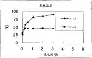
图33是表示实施例2和比较例2的白色光源装置(有荧光体圆拱罩)的输入功率为11W时基板温度与通电时间的相关性的图表。33 is a graph showing the correlation between substrate temperature and energization time when the input power of white light source devices (with phosphor domes) of Example 2 and Comparative Example 2 is 11W.
图34是表示实施例2和比较例2的白色光源装置(有荧光体圆拱罩)的Ra(平均现色评价数)与输入功率的相关性的图表。34 is a graph showing the correlation between Ra (average color rendering index) and input power of white light source devices (with phosphor domes) of Example 2 and Comparative Example 2. FIG.
具体实施方式Detailed ways
以下,根据具体实施方式详细说明本发明,但本发明的范围并不限于以下说明的实施方式。Hereinafter, the present invention will be described in detail based on specific embodiments, but the scope of the present invention is not limited to the embodiments described below.
<第1实施方式><First Embodiment>
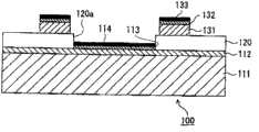
将第1实施方式的金属基板的剖面图示于图1。金属基板100具有在单侧整面层合有Ni层112的Al板111作为放热金属板。在Ni层112上的一部分上层合有绝缘树脂制的白色薄膜120。白色薄膜120上形成有由Cu箔131形成的布线图案。Cu箔131上依次层合有Ni层132和Au层133。白色薄膜120在其一部分具有贯通孔120a,在该贯通孔位置露出的Ni层112上,介由Ni层113层合有Au层114。Au层114的表面是光源搭载面。A cross-sectional view of the metal substrate of the first embodiment is shown in FIG. 1 . The
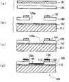
使用图2(a)~(d)对金属基板100的制备工序进行说明。The manufacturing process of the
首先,如图2(a)所示,在白色薄膜120的单面上层合Cu箔131,形成覆铜层合板。First, as shown in FIG. 2( a ),
接着,如图2(b)所示,蚀刻Cu箔131,形成布线图案,进一步使用尖头型冲裁模(···型·)等冲裁模,冲裁白色薄膜120的一部分,形成贯通孔120a。Next, as shown in FIG. 2( b ), the
接着,如图2(c)所示,在白色薄膜120的形成了布线图案(Cu箔131)的面的相反面上,作为放热金属板,通过真空加压,层合预先在单侧整面层合了Ni层112的Al板111。Al板111的厚度例如可以是0.1mm~5mm。实际上,可考虑要制备的金属基板100的尺寸,选择可获得必要强度的厚度的Al板111。Ni层112通过化学镀处理来形成。Al板111的化学镀Ni中,作为前处理,用碱等蚀刻Al板111表面,进一步用硝酸等进行酸处理,然后用碱性锌置换液进行锌置换。Ni层112的厚度可以是0.1μm~10μm。Next, as shown in FIG. 2(c), on the surface opposite to the surface of the
另外,Ni层112可通过真空蒸镀法或溅射法等干式法形成,这种情况下,无需锌置换处理。但是,湿式镀敷处理可以一并处理很多张Al板111,因此比干式法更适合大量生产。In addition, the
最后,如图2(d)所示,使用化学镀技术,在通过白色薄膜的贯通孔120a露出的Ni层112的表面依次形成Ni层113和Au层114。此时,同时在构成布线图案的Cu箔131的表面形成Ni层132和Au层133。该工序中形成的Ni层132的厚度优选2μm~8μm。Au层的厚度可以是0.01μm~10μm,为了使在Cu箔131上形成的Au层133的引线接合性良好,优选0.1μm以上,更优选0.3μm以上,进一步优选0.5μm以上。不过,即使形成得比这更薄,通过表面等离子体处理也可以改善Au层133的引线接合性。形成厚Au层会导致成本升高,因此该工序中形成的Au层的厚度优选2μm以下,更优选1μm以下。Finally, as shown in FIG. 2( d ), a
几乎全部树脂均不能牢固地粘合Au,但是在金属基板100中,不具有白色薄膜120层合在Au层114上的部分,其下表面整体与Ni层112相接,因此难以发生白色薄膜120的剥离。另外,除了布线图案上以外,只在搭载LED芯片的区域形成Au层,因此可以将昂贵的Au的使用量抑制为较少。Almost all resins cannot adhere to Au firmly, but in the
另外,Au的表面在波长低于550nm下的反射率显著降低,因此,Au在输出光中包含短波长可见光成分的光源装置、例如蓝色光源装置或白色光源装置中使用时,有时会使发光效率降低。为解决该问题,在金属基板100中,只将Au的使用限定于光源搭载面,并且用白色薄膜120覆盖光源搭载面以外的金属板表面,由此可以提高对可见光的反射率。In addition, the reflectance of the surface of Au at a wavelength lower than 550 nm is significantly reduced. Therefore, when Au is used in a light source device that includes a short-wavelength visible light component in the output light, such as a blue light source device or a white light source device, it may cause light emission. Reduced efficiency. To solve this problem, in the
此外,金属基板100中,在Au层114形成之前对Al板111进行2次镀Ni处理,因此在Al板111和Au层114之间用两个Ni层112、113间隔。因此,可以确实地防止Al和Au相接时产生的有害的合金化反应。In addition, in the
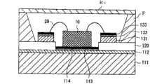
图3表示使用金属基板100构成的光源装置的剖面图。该光源装置是使用Au-Sn焊料等钎料(····)(·未·图示)将LED芯片10固定在作为光源搭载面的Au层114的表面,进一步通过接合线20与布线图案(Cu箔131)连接而获得。光源搭载面含有焊料湿润性良好的Au,因此LED芯片10与光源搭载面的结合很牢固。FIG. 3 shows a cross-sectional view of a light source device configured using the
在金属基板100上贴装LED芯片时,如图4所示,也可以使用基座。基座的使用对于贴装在半导体或由金属形成的导电性基板上形成有半导体发光元件结构的垂直电极型LED芯片特别有效。这种情况下,可优选使用如图5所示的极简单结构的基座。When mounting the LED chip on the
图5所示的基座30是在由AIN、氧化铝等形成的陶瓷板31的各主面31a、31b上分别具有镀金属层32、33而成的。陶瓷板31的厚度优选0.1mm~0.5mm,镀金属层32、33的厚度优选0.1μm~10μm。镀金属层32、33的最表层均由焊料湿润性良好的金属形成。此外,镀金属层32、33中的至少一方优选用焊料湿润性和引线接合性双方均优异的金属例如Au来形成最表层。使最表层为Au层的优选的镀金属层例如是:自与陶瓷板相接的一侧依次具有Ti/Pt/Au、Ti/Ni/Au、Cr/Au、Ti/Au等层合结构的多层膜。为了使引线接合性良好,Au层的厚度优选0.1μm以上,更优选0.3μm以上,特别优选0.5μm以上。形成厚Au层会导致成本提高,因此Au层的膜厚优选2μm以下,更优选1μm以下。The base 30 shown in FIG. 5 has metal plating layers 32 and 33 on the
图6表示使用上述基座30、将具备导电性基板的垂直电极型LED芯片11搭载在金属基板100上而成的光源装置的剖面图。该光源装置中,提供光源搭载面的Au层114与基座30(镀金属层32)之间、以及基座30(镀金属层33)与LED芯片11之间分别通过焊料(未图示)连接。LED芯片11上表面侧的电极通过接合线21与一布线图案连接。另一方面,LED芯片11的下表面侧的电极经由镀金属层33和接合线22与另一布线图案连接。Al基板111和LED芯片11之间通过基座30所含的陶瓷板31被绝缘。6 shows a cross-sectional view of a light source device in which a vertical electrode type LED chip 11 having a conductive substrate is mounted on a
垂直电极型LED芯片11例如是:美国专利公开公报2006/0154389号说明书中公开的在芯片中具有金属基板作为支撑基板的LED芯片、日本特开2006-179511号公报所公开的使用GaN基板制备的LED芯片、Japanese Journal of Applied Physics第49卷022101页(2010年)公开的在芯片中具有半导体基板(Si基板)作为支撑基板的LED芯片等。The vertical electrode type LED chip 11 is, for example: the LED chip disclosed in the specification of U.S. Patent Publication No. 2006/0154389, which has a metal substrate as a supporting substrate in the chip, and the LED chip prepared by using a GaN substrate disclosed in Japanese Patent Application Laid-Open No. 2006-179511. LED chips, Japanese Journal of Applied Physics volume 49, page 022101 (2010) disclose LED chips having a semiconductor substrate (Si substrate) as a supporting substrate in the chip, and the like.
将使用了导电性基板的水平电极型LED芯片、即从设置有正负电极一侧的芯片面获取光的类型的LED芯片搭载在金属基板100上时,也可优选使用上述基座30。这样的LED芯片例如记载于国际公开第2008/004437号(使用了GaN基板的LED芯片)。如果使用基座30,则通过陶瓷板31将LED芯片的导电性基板与金属基板的放热金属板绝缘,因此可防止漏电,除此之外在一个金属基板上搭载多个LED芯片时,芯片之间布线的自由度提高。The
<第2实施方式><Second embodiment>
图7表示第2实施方式的金属基板的剖面图。金属基板200具有在单侧整面层合有Ni层212的Al板211作为放热金属板。Ni层212上的一部分上层合有绝缘树脂制的第一白色薄膜221。第一白色薄膜221上形成有由Cu箔231形成的布线图案,同时以使该布线图案的一部分露出的方式层合有绝缘树脂制的第二白色薄膜222。在Cu箔231的一部分露出的表面上依次层合有Ni层232和Au层233。第一白色薄膜221和第二白色薄膜222在其一部分上分别具有贯通孔221a、222a,在这些贯通孔的位置所露出的Ni层212上介由Ni层213层合有Au层214。Au层214的表面是光源搭载面。FIG. 7 shows a cross-sectional view of a metal substrate according to a second embodiment. The
使用图8(a)~(d)说明金属基板200的制备工序。The manufacturing process of the
首先,如图8(a)所示,在第一白色薄膜221的单面层合Cu箔231,形成覆铜层合板。First, as shown in FIG. 8( a ),
接着,如图8(b)所示,蚀刻Cu箔231,形成布线图案,进一步使用尖头型冲裁模冲裁第一白色薄膜221的一部分,形成第一贯通孔221a。Next, as shown in FIG. 8( b ), the
此外,在另外的工序中,准备由与第一白色薄膜221相同的绝缘树脂材料形成的第二白色薄膜222。在该第二白色薄膜222上通过使用尖头型冲载模的冲载加工预先形成第二贯通孔222a。第二白色薄膜222成为用于保护在第一白色薄膜221上形成的布线图案(Cu箔231)的保护层。如图所示,第二白色薄膜222的贯通孔222a(50)设定成如下的形状和尺寸,即,使第一白色薄膜221的贯通孔221a收纳在其内侧,并且使由Cu箔231形成的布线图案的一部分(形成引线接合端子的部分)露出。In addition, in another process, the second
接着,如图8(c)所示,通过真空加压,在第一白色薄膜221的形成了布线图案(Cu箔231)的面的相反面上层合预先在单侧整面层合了Ni层212的Al板211。该真空加压工序中,也可同时在第一白色薄膜221上层合第二白色薄膜222。Next, as shown in FIG. 8(c), by applying vacuum pressure, a Ni layer previously laminated on one side of the entire surface is laminated on the surface opposite to the surface of the first
最后,如图8(d)所示,使用化学镀技术,在通过第一白色薄膜221的贯通孔221a和通过第二白色薄膜222的贯通孔222a而露出的Ni层212的表面上依次形成Ni层213和Au层214。此时,同时在布线图案(Cu箔231)的一部分露出的表面上形成Ni层232和Au层233。Finally, as shown in FIG. 8( d), using electroless plating technology, Ni is sequentially formed on the surface of the
金属基板200中的Al板、Ni层和Au层的优选厚度请参照第1实施方式的金属基板100中对应结构的优选厚度。For the preferred thicknesses of the Al plate, Ni layer and Au layer in the
图9表示使用金属基板200构成的光源装置的剖面图。该光源装置是使用Au-Sn焊料等钎料(未图示)将LED芯片10固定在作为光源搭载面的Au层214的表面,并且通过接合线20与布线图案连接而获得。光源搭载面含有焊料湿润性良好的Au,因此LED芯片与光源搭载面的结合很牢固。LED芯片包含导电性基板,在使该导电性基板朝向光源搭载面侧地固定该LED芯片时,可优选使用上述基座30。FIG. 9 shows a cross-sectional view of a light source device configured using a
<第3实施方式><third embodiment>
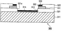
图10表示第3实施方式的金属基板的剖面图。金属基板300具有Cu板311作为放热金属板。在Cu板311上的一部分上层合有绝缘树脂制的第一白色薄膜321。在第一白色薄膜321上形成有由Cu箔331形成的布线图案,同时以使该布线图案(Cu箔331)的一部分露出的方式层合有绝缘树脂制的第二白色薄膜322。在布线图案(Cu箔331)的一部分露出的表面上依次层合有Ni层332和Au层333。第一白色薄膜321和第二白色薄膜322在其一部分上分别具有贯通孔321a、322a,在这些贯通孔的位置所露出的Cu板311的表面上介由Ni层313层合有Au层314。Au层314的表面是光源搭载面。FIG. 10 shows a cross-sectional view of a metal substrate according to a third embodiment. The
使用图11(a)~(d)说明金属基板300的制备工序。The manufacturing process of the
首先,如图11(a)所示,在第一白色薄膜321的单面层合Cu箔331,形成覆铜层合板。First, as shown in FIG. 11( a ),
接着,如图11(b)所示,蚀刻Cu箔331,形成布线图案,进一步使用尖头型冲裁模冲裁第一白色薄膜的一部分,形成贯通孔321a。Next, as shown in FIG. 11( b ), the
此外,在另外的工序中,准备由与第一白色薄膜321相同的绝缘树脂材料形成的第二白色薄膜322。在该第二白色薄膜322上通过使用尖头型冲载模的冲载加工形成第二贯通孔322a。第二白色薄膜322成为用于保护在第一白色薄膜321上形成的布线图案(Cu箔331)的保护层。如图所示,第二白色薄膜322的贯通孔322a设定成如下的形状和尺寸,即,使第一白色薄膜321的贯通孔321a收纳在其内侧,并且使布线图案(Cu箔331)的一部分(形成引线接合端子的部分)露出。In addition, in another process, the second
接着,如图11(c)所示,通过真空加压,在第一白色薄膜321的形成了布线图案(Cu箔331)的面的相反面上层合Cu板311。该真空加压工序中,也可同时在第一白色薄膜321上层合第二白色薄膜322。Next, as shown in FIG. 11( c ), a
最后,如图11(d)所示,使用化学镀技术,在通过第一白色薄膜的贯通孔321a和通过第二白色薄膜的贯通孔322a而露出的Cu板311的表面上依次形成Ni层313和Au层314。此时,同时在布线图案(Cu箔331)的一部分露出的表面上形成Ni层332和Au层333。Finally, as shown in FIG. 11( d), using electroless plating technology, a
金属基板300中,Ni层313作为防止Cu从Cu板311向Au层314扩散的阻挡层发挥作用。Cu的扩散会使Au层表面的焊料湿润性降低。In the
金属基板300中的Cu板、Ni层和Au层的优选厚度请参照第1实施方式的金属基板100中对应结构的优选厚度。For the preferred thicknesses of the Cu plate, Ni layer and Au layer in the
金属基板300中,也不具有第一白色薄膜321层合在Au层314上的部分,其下表面整体与Cu板311相接,因此,难以发生第一白色薄膜321的剥离。在变形例中,除了在Cu板311的形成有光源搭载面一侧的整个面上层合Ni层,还可以将第一白色薄膜321层合在该Ni层上。The
图12表示使用第3实施方式的金属基板300构成的光源装置的剖面图。该光源装置是使用Au-Sn焊料等钎料(未图示)将LED芯片10固定在作为光源搭载面的Au层314的表面,并且通过接合线20与布线图案连接而获得。光源搭载面含有焊料湿润性良好的Au,因此LED芯片与光源搭载面的结合很牢固。LED芯片包含导电性基板,以使该导电性基板朝向光源搭载面侧地固定该LED芯片时,可优选使用上述基座30。FIG. 12 is a cross-sectional view of a light source device configured using the
上述各实施方式中,含有白色薄膜和形成图案的Cu箔的布线基板可以根据需要制成多层构成(多层布线基板)。另外,在白色薄膜上形成贯通孔的方法并不限于上述使用尖头型冲裁模的方法,例如,可以是采用激光加工或钻孔加工的方法。In each of the above-described embodiments, the wiring board including the white thin film and the patterned Cu foil may be multilayered (multilayer wiring board) as needed. In addition, the method of forming the through-hole in the white film is not limited to the above-mentioned method using a pointed die, for example, a method using laser processing or drilling may be used.
上述各实施方式的金属基板的制造工序说明中使用的附图(图2、8和11)中只描述了1个金属基板,但这只是为了方便说明。为了进行大量生产,可采用如下方法,即,使用大面积的放热金属板同时形成很多金属基板、然后切分的方法。The drawings ( FIGS. 2 , 8 , and 11 ) used in the description of the manufacturing steps of the metal substrates according to the above-mentioned embodiments describe only one metal substrate, but this is for convenience of description. For mass production, a method of simultaneously forming many metal substrates using a large-area exothermic metal plate and then dicing them may be employed.
可在上述各实施方式的金属基板上搭载的LED芯片没有限定,可以搭载使用了AlGaAs系半导体的红色LED芯片、使用了AlGaInP系半导体的黄色LED芯片、使用了GaP系半导体的绿色LED芯片、使用了ZnSe系半导体的绿-蓝色LED芯片、使用了AlGaInN系半导体的绿色~紫外LED芯片、使用了ZnO系半导体的蓝色~紫外LED芯片等各种LED芯片。此外,光源搭载面的尺寸可根据要搭载的LED芯片的尺寸和数量适当设定。The LED chip that can be mounted on the metal substrate of each of the above-mentioned embodiments is not limited, and a red LED chip using an AlGaAs-based semiconductor, a yellow LED chip using an AlGaInP-based semiconductor, a green LED chip using a GaP-based semiconductor, etc. can be mounted. Green-blue LED chips using ZnSe-based semiconductors, green-ultraviolet LED chips using AlGaInN-based semiconductors, blue-ultraviolet LED chips using ZnO-based semiconductors, and other LED chips. In addition, the size of the light source mounting surface can be appropriately set according to the size and number of LED chips to be mounted.
使用上述各实施方式的金属基板制备光源装置时,光源搭载面与LED芯片的接合所使用的优选的接合材料是焊料(钎料)。LED芯片的表面也可根据需要进行镀金属,以使利用焊料的接合牢固地进行。When producing a light source device using the metal substrate of each of the above embodiments, solder (solder) is a preferable bonding material used for bonding the light source mounting surface and the LED chip. The surface of the LED chip may also be metal-plated as needed so that bonding with solder can be firmly performed.
上述各实施方式中,固定在光源搭载面上的LED芯片可以用透明的树脂或玻璃来封装。对于优选的封装材料,参考公知技术即可,最优选的封装材料之一是有机硅树脂。其理由是:可见波长区域的透明性和耐光性优异。封装材料的成型方法没有限定,可以任意采用灌封成型、模具成型等本领域通常采用的方法。In each of the above-mentioned embodiments, the LED chips fixed on the light source mounting surface may be packaged with transparent resin or glass. As for the preferred encapsulating material, reference may be made to known techniques, and one of the most preferred encapsulating materials is silicone resin. The reason for this is that it is excellent in transparency and light resistance in the visible wavelength region. The molding method of the packaging material is not limited, and methods commonly used in the field such as potting molding and mold molding can be used arbitrarily.
<变形实施方式><Modified embodiment>
上述各实施方式的金属基板均在光源搭载面侧具有凹腔。即,是以在白色薄膜上设置的贯通孔的表面作为侧壁、以光源搭载面作为底面的凹腔。该凹腔的深度可通过改变白色薄膜的膜厚来调节。The metal substrates in each of the above-mentioned embodiments have a concave cavity on the side of the light source mounting surface. That is, it is a concave cavity with the surface of the through-hole provided in the white film as the side wall and the light source mounting surface as the bottom surface. The depth of the cavity can be adjusted by changing the film thickness of the white film.
如图13示出的金属基板400所示,可以使凹腔的侧壁倾斜,以使得从固定在光源搭载面上的LED芯片向侧面射出的光被凹腔的侧壁反射,而被导到凹腔的开口方向。为了获得所述构成,在白色薄膜420上设置贯通孔420a时,可以使其截面积沿薄膜的膜厚方向变化。这里所说的截面积,是用与白色薄膜的的厚度方向正交的平面切断贯通孔而形成的截面的面积。As shown in the
本发明的金属基板中,作为基材的放热金属板与树脂板相比,刚性、热稳定性等优异,此外,与陶瓷板不同,具有不易破碎的性质,因此,例如可形成为超过10cm见方的大面积。增大面积时,如图14示出的金属基板500所示,优选设置多个上述凹腔。本发明的金属基板的特征、即白色薄膜难以从放热金属板上剥离,对于制备大面积产品也发挥有利作用。In the metal substrate of the present invention, the exothermic metal plate used as the base material is superior in rigidity, thermal stability, etc. compared to a resin plate, and also has the property that it is not easy to break, unlike a ceramic plate. Square large area. When increasing the area, as shown in the
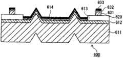
本发明的金属基板可以具备通过加工放热金属板而形成的凹腔。图15是表示这样的金属基板的一个例子的剖面图。金属基板600具备在单侧整面层合有Ni层612的Al板611作为放热金属板。该放热金属板通过压制加工,形成向Ni层612侧突出的凸部。该凸部的平面形状为环状。在白色薄膜620上形成的贯通孔成型为具有比该环状凸部外径大的直径的圆形。因此,在层合白色薄膜620和放热金属板后,通过化学镀法形成的Ni层613和Au层614也覆盖该环状凸部的表面。该例子中,向光源搭载面(Au层614的表面)内突出的环状凸部的内侧是凹腔。The metal substrate of the present invention may include a concave cavity formed by processing a heat-dissipating metal plate. FIG. 15 is a cross-sectional view showing an example of such a metal substrate. The
图16是表示具备通过加工放热金属板而形成的凹腔的金属基板的另一例子的剖面图。金属基板700具备在单侧整面层合有Ni层712的Al板711作为放热金属板。该放热金属板上通过压制加工,形成向Ni层712侧突出的凸部。该凸部的平面形状为环状。在白色薄膜720上形成其尺寸可收纳在该环状凸部内侧的贯通孔。在层合白色薄膜720和放热金属板后,通过化学镀处理形成Ni层713和Au层714,由此在环状凸部的内侧(凹腔内)形成光源搭载面(Au层714的表面)。环状凸部的表面被白色薄膜720覆盖,因此具有高的光反射性。16 is a cross-sectional view showing another example of a metal substrate provided with cavities formed by processing a heat dissipation metal plate. The
<白色光源装置的构成例子><Configuration example of white light source device>
以下对于使用上述第1实施方式的金属基板100得到的白色光源装置的构成例子进行说明。A configuration example of a white light source device obtained by using the
需要说明的是,对于本发明的缩写,例如“Y2SiO5:Ce,Tb”是指包含“Y2SiO5:Ce”、“Y2SiO5:Tb”和“Y2SiO5:Ce,Tb”的总称,此外,“(La,Y)2O2S:Eu”是指包含“La2O2S:Eu”、“LaxY2-xO2S:Eu(0<x<2)”和“Y2O2S:Eu”的总称。It should be noted that for the abbreviation of the present invention, for example, "Y2 SiO5 :Ce, Tb" refers to including "Y2 SiO5 :Ce", "Y2 SiO5 :Tb" and "Y2 SiO5 :Ce , Tb", in addition, "(La, Y)2 O2 S:Eu" refers to "La2 O2 S:Eu", "Lax Y2-x O2 S:Eu(0<x <2)" and "Y2 O2 S:Eu" in general.
图17中给出了剖面图的光源装置是在金属基板100上贴装蓝色LED芯片10,并通过树脂模塑件M封装而成的。对于与第1实施方式同样的部件,标以相同编号,并省略其说明。该光源装置可以通过使YAG:Ce等黄色荧光体分散于树脂模塑件M中来制成白色光源装置。此外,除黄色荧光体之外还使用(Mg,Ca,Sr,Ba)AlSiN3:Eu等红色荧光体,则可得到色温更低的白色光源装置。为了获得现色性更高的白色光源装置,可以将黄色荧光体的一部分或全部置换为(Ba,Ca,Sr,Mg)2SiO4:Eu、Eu激活β-SiAlON、(Ba,Sr,Ca)3Si6O12N2:Eu等绿色荧光体。荧光体也可以以有机硅树脂作为粘合剂而涂布在蓝色LED芯片10的表面,以此来替代分散于树脂模塑件M中。The light source device shown in sectional view in FIG. 17 is formed by mounting a
在图17所示的光源装置中,使用近紫外LED芯片或紫色LED芯片代替蓝色LED芯片时,如果在封装材料中添加(Ba,Sr,Ca)MgAl10O17:Eu、(Ca,Sr,Ba)5(PO4)3Cl:Eu等蓝色荧光体和YAG:Ce等黄色荧光体,则可获得白色光源装置。这种情况下,除了黄色荧光体之外还添加红色荧光体,则可获得色温更低的白色光源装置,另外,通过将黄色荧光体的一部分或全部置换为绿色荧光体,可以改善现色性。红色荧光体和绿色荧光体可以使用上述所例举的物质。In the light source device shown in Figure 17, when using near-ultraviolet LED chips or purple LED chips instead of blue LED chips, if (Ba, Sr, Ca)MgAl10 O17 :Eu, (Ca, Sr , Ba)5 (PO4 )3 Cl:Eu and other blue phosphors and YAG:Ce and other yellow phosphors, a white light source device can be obtained. In this case, by adding a red phosphor in addition to the yellow phosphor, a white light source device with a lower color temperature can be obtained, and by substituting part or all of the yellow phosphor with a green phosphor, color rendering can be improved . As the red phosphor and the green phosphor, those listed above can be used.
图18中给出了剖面图的光源装置是在金属基板100上贴装蓝色LED芯片10,然后使荧光体圆拱罩覆盖蓝色LED芯片而成的白色光源装置。对于与第1实施方式同样的部件,标以相同编号,并省略其说明。荧光体圆拱罩RD是将使荧光体分散在透明树脂中而成的透光性组合物成型成圆拱罩状而得到的。添加到荧光体圆拱罩中的荧光体与上述例子中分散于树脂模塑件中的荧光体相同。The light source device shown in sectional view in FIG. 18 is a white light source device in which a
图19中给出了剖面图的光源装置是在金属基板100上贴装蓝色LED芯片10,然后支撑体使用框体F,并在蓝色LED芯片上配置荧光体片RS而成的白色光源装置。对于与第1实施方式同样的部件,标以相同编号,并省略其说明。荧光体片RS是将使荧光体分散在透明树脂中而成的透光性组合物成型成片状而得到的。添加到荧光体片Rs中的荧光体与上述例子中分散于树脂模塑件中的荧光体相同。The light source device with a sectional view shown in FIG. 19 is a
图18和图19所示的光源装置中,将荧光体圆拱罩或荧光体片配置在离蓝色LED芯片有空间距离的位置。即,以夹持空隙的方式配置在与金属基板的光源搭载面和LED芯片有空间距离的位置上,因此,由于空隙产生的隔热效果,可以抑制LED芯片发热所导致的温度升高。其结果,由于热导致的荧光体效率的降低和劣化得到抑制。并且,在荧光体含有层形成为圆拱罩状的图18的例子中,与荧光体含有层形成为平面片状的图19的例子相比,荧光体所受到的激发光的能量密度低,因此荧光体因波长转换损耗所带来的发热小。因此,可以说这是对LED芯片输入数W以上的大功率时特别优选的方案。In the light source device shown in FIGS. 18 and 19 , the phosphor dome or the phosphor sheet is arranged at a position with a spatial distance from the blue LED chip. That is, it is arranged at a position with a space between the light source mounting surface of the metal substrate and the LED chip with the gap sandwiched therebetween. Therefore, due to the heat insulation effect of the gap, the temperature rise caused by the heat generation of the LED chip can be suppressed. As a result, reduction in phosphor efficiency and deterioration due to heat are suppressed. In addition, in the example of FIG. 18 in which the phosphor-containing layer is formed in a dome shape, the energy density of the excitation light received by the phosphor is lower than that in the example of FIG. 19 in which the phosphor-containing layer is formed in a planar sheet shape. Therefore, the heat generated by the phosphor due to wavelength conversion loss is small. Therefore, it can be said that this is particularly preferable when a large power of several W or more is input to the LED chip.
以下给出可优选用于上述例举的白色光源装置中的荧光体的具体例子。Specific examples of phosphors that can be preferably used in the above-exemplified white light source devices are given below.
作为蓝色荧光体,可举出BaMgAl10O17:Eu、(Sr,Ba,Ca)5(PO4)3Cl:Eu等。Examples of the blue phosphor include BaMgAl10 O17 :Eu, (Sr, Ba, Ca)5 (PO4 )3 Cl:Eu, and the like.
作为绿色荧光体,可举出(Ba,Sr,Ca,Mg)2SiO4:Eu、Eu激活β-SiAlON、(Ba,Sr,Ca)3Si6O12N2:Eu、Ca3(ScMg)5O12:Ce、CaSc2O4:Ce、BaMgAl10O17:Eu,Mn等。Examples of green phosphors include (Ba, Sr, Ca, Mg)2 SiO4 :Eu, Eu activated β-SiAlON, (Ba, Sr, Ca)3 Si6 O12 N2 :Eu, Ca3 (ScMg )5 O12 :Ce, CaSc2 O4 :Ce, BaMgAl10 O17 :Eu, Mn, etc.
作为黄色荧光体,可举出YAG:Ce、TAG:Ce、La3Si6N11:Ce等用Ce激活的荧光体,除此之外,也可以使用用Eu激活的SiAlON型的氮氧化物荧光体Cax(Si,Al)12(O,N)15:Eu等。Examples of yellow phosphors include phosphors activated by Ce, such as YAG:Ce, TAG:Ce, and La3 Si6 N11 :Ce. In addition, SiAlON-type oxynitrides activated by Eu can also be used. Phosphor Cax (Si, Al)12 (O, N)15 :Eu, etc.
作为红色荧光体,可举出(Mg,Ca,Sr,Ba)AlSiN3:Eu、(Mg,Ca,Sr,Ba)2(Si,Al)5Na:Eu、(Mg,Ca,Sr,Ba)AlSi(N,O)3:Eu、Eu激活α-SiAlON、SrAlSi4N7:Eu、(Sr,Ba,Ca)3SiO5:Eu、K2SiF6:Mn、K2TiF6:Mn等。Examples of red phosphors include (Mg, Ca, Sr, Ba)AlSiN3 :Eu, (Mg, Ca, Sr, Ba)2 (Si, Al)5Na :Eu, (Mg, Ca, Sr, Ba)AlSi(N,O)3 :Eu, Eu activates α-SiAlON, SrAlSi4 N7 :Eu, (Sr,Ba,Ca)3 SiO5 :Eu, K2 SiF6 :Mn, K2 TiF6 : Mn et al.
<白色薄膜><White film>
以下,对于上述各实施方式的金属基板中所使用的白色薄膜,详细说明其优选的实施方式。Hereinafter, preferred embodiments of the white thin film used for the metal substrate of each of the above-mentioned embodiments will be described in detail.
上述各实施方式的金属基板中所使用的、绝缘树脂制的白色薄膜由以热塑性树脂或热固化性树脂作为基础树脂、混合白色颜料而成的树脂组合物构成。白色薄膜上形成布线图案时(以白色薄膜作为布线基板的绝缘板时),特别是在该布线图案上形成引线接合用端子时,白色薄膜必须硬到可引线接合的程度。这种情况下的白色薄膜的优选基础树脂,作为热固化性树脂,可例举酚醛树脂、环氧树脂、聚酰亚胺树脂。此外,作为热塑性树脂,可例举后述的高耐热性的热塑性树脂。将以热固化性树脂为基础的白色薄膜层合在放热金属板上时,优选使用粘合剂。The white film made of insulating resin used in the metal substrate of each of the above-mentioned embodiments is composed of a resin composition in which a thermoplastic resin or a thermosetting resin is used as a base resin and a white pigment is mixed. When forming a wiring pattern on the white film (when using the white film as an insulating plate of the wiring substrate), especially when forming wire bonding terminals on the wiring pattern, the white film must be hard enough to allow wire bonding. A preferable base resin for the white film in this case is a thermosetting resin that may, for example, be a phenolic resin, an epoxy resin, or a polyimide resin. Moreover, as a thermoplastic resin, the high heat-resistant thermoplastic resin mentioned later is mentioned. It is preferable to use an adhesive when laminating a thermosetting resin-based white film on an exothermic metal plate.
不将白色薄膜作为布线基板的绝缘板使用、而只作为反射材料来使用时,可以使用有机硅树脂作为其基础树脂。这种情况下,以热固化性树脂为基础的白色薄膜可通过在放热金属板的表面涂布未固化的白色树脂组合物、并使该涂布膜加热固化的方法来形成,以此代替将预先成型为薄膜的材料层合在放热金属板上。When using the white film not as an insulating plate of a wiring board but only as a reflective material, a silicone resin can be used as the base resin. In this case, a white film based on a thermosetting resin can be formed by coating an uncured white resin composition on the surface of an exothermic metal plate and heating and curing the coated film, instead of The material preformed into a film is laminated to an exothermic metal sheet.
也作为布线基板的绝缘板发挥作用的白色薄膜所适合的热塑性树脂材料,例如有:聚醚醚酮(PEEK)、聚醚酮(PEK)、聚苯硫醚(PPS)、聚醚砜(PES)、聚苯醚(PPE)、聚酰胺酰亚胺(PAI)、聚醚酰亚胺(PEI)、聚苯砜(PPSU)、液晶聚合物(LCP)。其中,由于耐热性的原因,特别优选使用选自晶体熔解峰温度为260℃以上的结晶性热塑性树脂、玻璃化转变温度为260℃以上的非晶性热塑性树脂、以及液晶转变温度为260℃以上的液晶聚合物中的任意一种以上。更进一步优选使用选自晶体熔解峰温度(Tm)为260℃以上的结晶性热塑性树脂、以及玻璃化转变温度(Tg)为260℃以上的非晶性热塑性树脂中的任意一种以上。通过基础树脂使用晶体熔解峰温度、玻璃化转变温度或液晶转变温度满足上述条件的热塑性树脂,可得到在无Pb焊料的回流焊工序中也几乎没有变色的、耐热性优异的白色薄膜。特别是考虑了使用AuSn浆的LED芯片贴装工序时,回流焊温度为300℃以上,因此进一步优选使用选自晶体熔解峰温度为300℃以上的结晶性热塑性树脂、玻璃化转变温度为300℃以上的非晶性热塑性树脂、以及液晶转变温度为300℃以上的液晶聚合物中的任意一种以上。作为晶体熔解峰温度为260℃以上的结晶性热塑性树脂,可优选使用聚醚醚酮(PEEK:Tg=145℃,Tm=335℃)、聚醚酮(PEK:Tg=165℃,Tm=355℃)等的聚芳酮(PAr)、聚苯硫醚(PPS:Tg=100℃,Tm=280℃)等。作为玻璃化转变温度为260℃以上的非晶性热塑性树脂,可优选使用聚酰胺酰亚胺(PAI:Tg=280℃)或具有260℃以上的具有高Tg的聚醚酰亚胺(PEI)等。Suitable thermoplastic resin materials for white films that also function as insulating plates for wiring substrates include: polyether ether ketone (PEEK), polyether ketone (PEK), polyphenylene sulfide (PPS), polyether sulfone (PES) ), polyphenylene ether (PPE), polyamideimide (PAI), polyetherimide (PEI), polyphenylene sulfone (PPSU), liquid crystal polymer (LCP). Among them, it is particularly preferable to use a crystalline thermoplastic resin having a crystal melting peak temperature of 260° C. or higher, an amorphous thermoplastic resin having a glass transition temperature of 260° C. or higher, and a liquid crystal transition temperature of 260° C. or more due to heat resistance. Any one or more of the above liquid crystal polymers. It is still more preferable to use any one or more selected from crystalline thermoplastic resins having a crystal melting peak temperature (Tm) of 260°C or higher and amorphous thermoplastic resins having a glass transition temperature (Tg) of 260°C or higher. By using a thermoplastic resin whose crystal melting peak temperature, glass transition temperature, or liquid crystal transition temperature satisfies the above conditions as a base resin, it is possible to obtain a white film with almost no discoloration in the reflow process of Pb-free solder and excellent heat resistance. In particular, when considering the LED chip mounting process using AuSn paste, the reflow temperature is 300°C or higher, so it is more preferable to use a crystalline thermoplastic resin with a crystal melting peak temperature of 300°C or higher and a glass transition temperature of 300°C. Any one or more of the above amorphous thermoplastic resins and liquid crystal polymers having a liquid crystal transition temperature of 300° C. or higher. As a crystalline thermoplastic resin having a crystal melting peak temperature of 260°C or higher, polyetheretherketone (PEEK: Tg = 145°C, Tm = 335°C), polyetherketone (PEK: Tg = 165°C, Tm = 355°C) can be preferably used. °C), polyarylketone (PAr), polyphenylene sulfide (PPS: Tg=100°C, Tm=280°C), etc. As an amorphous thermoplastic resin having a glass transition temperature of 260°C or higher, polyamideimide (PAI: Tg = 280°C) or polyetherimide (PEI) having a high Tg of 260°C or higher can be preferably used wait.
上述例举的结晶性热塑性树脂可以单独使用一种,或者作为将多种混合而得到的混合树脂组合物的形式使用。该结晶性热塑性树脂可以作为将聚醚酰亚胺(PEI)等非晶性热塑性树脂混合而成的混合树脂组合物的形式使用。其中,关于基础树脂使用含有80~20%质量的晶体熔解峰温度为260℃以上的结晶性聚芳酮树脂(A)、和20~80%质量的非晶性聚醚酰亚胺树脂(B)的树脂组合物而得到的白色薄膜,其与金属板和金属箔的密合性、以及制备带布线图案保护层的基板或多层布线基板时所必需的薄膜之间的粘合性优异,同时具有在无Pb焊料的回流焊工序中几乎不变色的优异的耐热性。The above-exemplified crystalline thermoplastic resins may be used alone or in the form of a mixed resin composition obtained by mixing a plurality of them. This crystalline thermoplastic resin can be used as a mixed resin composition obtained by mixing an amorphous thermoplastic resin such as polyetherimide (PEI). Among them, as the base resin, a crystalline polyarylketone resin (A) containing 80 to 20% by mass of a crystal melting peak temperature of 260° C. or higher and an amorphous polyetherimide resin (B) of 20 to 80% by mass are used. ) resin composition, which has excellent adhesion to metal plates and metal foils, and excellent adhesion between films necessary for the production of substrates with wiring pattern protective layers or multilayer wiring substrates, At the same time, it has excellent heat resistance that hardly changes color in the reflow process of Pb-free solder.
从提高耐热性的角度考虑,上述含有结晶性聚芳酮树脂(A)和非晶性聚醚酰亚胺树脂(B)的树脂组合物优选聚芳酮树脂(A)的含有率为20%质量以上,更优选30%质量以上,进一步优选40%质量以上。另一方面,若聚芳酮树脂(A)的含有率过高,则组合物的结晶性提高,与金属板和金属箔的密合性、以及使用由该组合物制成的白色薄膜制备带布线图案保护层的布线基板或多层布线基板时所必需的薄膜之间的密合性有降低倾向。因此,该树脂组合物中聚芳酮树脂(A)的含有率优选80%质量以下,更优选75%质量以下,进一步优选70%质量以下。From the viewpoint of improving heat resistance, the resin composition containing the above-mentioned crystalline polyarylketone resin (A) and amorphous polyetherimide resin (B) preferably has a content rate of polyarylketone resin (A) of 20%. % by mass or more, more preferably 30% by mass or more, still more preferably 40% by mass or more. On the other hand, if the content of the polyarylketone resin (A) is too high, the crystallinity of the composition improves, the adhesiveness with metal plates and metal foils, and the use of white films made of the composition to prepare tapes Adhesiveness between thin films required for wiring boards or multilayer wiring boards of the wiring pattern protective layer tends to be lowered. Therefore, the content of the polyarylketone resin (A) in the resin composition is preferably not more than 80% by mass, more preferably not more than 75% by mass, and still more preferably not more than 70% by mass.
上述结晶性聚芳酮系树脂(A)是在其结构单元中含有芳环键、醚键和酮键的热塑性树脂。其具体例子可例举:聚醚酮(玻璃化转变温度[以下称为“Tg”]:157℃,晶体熔解峰温度[以下称为“Tm”]:373℃)、聚醚醚酮(Tg=143℃,Tm=334℃)、聚醚醚酮酮(Tg=153℃,Tm=370℃)等。其中,从耐热性的角度考虑,优选的是Tm为260℃以上、特别是300~380℃的材料。只要不妨碍本发明的效果,结晶性聚芳酮系树脂(A)可以含有联苯结构、磺酰基等或其它的重复单元。The above-mentioned crystalline polyarylketone-based resin (A) is a thermoplastic resin containing an aromatic ring bond, an ether bond, and a ketone bond in its structural unit. Specific examples thereof include polyether ketone (glass transition temperature [hereinafter referred to as "Tg"]: 157°C, crystal melting peak temperature [hereinafter referred to as "Tm"]: 373°C), polyetheretherketone (Tg =143°C, Tm=334°C), PEEK (Tg=153°C, Tm=370°C), etc. Among them, a material having a Tm of 260°C or higher, particularly 300 to 380°C, is preferable from the viewpoint of heat resistance. The crystalline polyarylketone-based resin (A) may contain a biphenyl structure, a sulfonyl group, or other repeating units as long as the effects of the present invention are not inhibited.
上述结晶性聚芳酮系树脂(A)中,特别优选的是以具有下述结构式(1)所示重复单元的聚醚醚酮为主成分的聚芳酮系树脂。这里,主成分是指其含量超过50%重量。市售的聚醚醚酮有:VICTREX公司制备的商品名“PEEK151G”(Tg=143℃,Tm=334℃)、“PEEK381G”(Tg=143℃,Tm=334℃)、PEEK450G”(Tg=143℃,Tm=334℃)等。另外,也可以将符合聚芳酮系树脂(A)的2种以上的聚芳酮系树脂组合使用。Among the above-mentioned crystalline polyarylketone-based resins (A), polyarylketone-based resins mainly composed of polyether ether ketone having a repeating unit represented by the following structural formula (1) are particularly preferable. Here, the main component means that its content exceeds 50% by weight. Commercially available polyetheretherketones include: trade names "PEEK151G" (Tg=143°C, Tm=334°C), "PEEK381G" (Tg=143°C, Tm=334°C), PEEK450G" (Tg=143°C, Tm=334°C) produced by VICTREX Corporation 143°C, Tm=334°C), etc. In addition, two or more polyarylketone-based resins corresponding to the polyarylketone-based resin (A) may be used in combination.

作为上述非晶性聚醚酰亚胺树脂(B)的具体例子,可举出具有下述结构式(2)或(3)所示的重复单元的非晶性聚醚酰亚胺树脂。Specific examples of the above-mentioned amorphous polyetherimide resin (B) include an amorphous polyetherimide resin having a repeating unit represented by the following structural formula (2) or (3).

具有结构式(2)或(3)所示的重复单元的非晶性聚醚酰亚胺树脂,可以按照公知的方法,以4,4’-[亚异丙基双(对苯氧基)]二邻苯二甲酸酐与对苯二胺或间苯二胺的缩聚物的形式制备。作为这些非晶性聚醚酰亚胺树脂的市售商品,可举出General Electric公司制备的商品名“Ultem 1000”(Tg=216℃)、“Ultem 1010”(Tg=216℃)或“UltemCRS5001”(Tg=226℃)等。其中,特别优选具有上述结构式(2)所示的重复单元的非晶性聚醚酰亚胺树脂。另外,也可以将符合聚醚酰亚胺树脂(B)的2种以上的聚醚酰亚胺树脂组合使用。The non-crystalline polyetherimide resin having the repeating unit shown in structural formula (2) or (3) can be according to known method, with 4,4'-[isopropylidene bis(p-phenoxy)] It is prepared in the form of polycondensate of diphthalic anhydride and p-phenylenediamine or m-phenylenediamine. Commercially available products of these amorphous polyetherimide resins include trade names "
上述优选的热塑性树脂材料可以作为添加了无机填充材料的组合物的形式供给白色薄膜的形成。作为无机填充材料,可举出例如滑石、云母、云母、玻璃鳞片、氮化硼(BN)、碳酸钙、氢氧化铝、二氧化硅、钛酸盐(钛酸钾等)、硫酸钡、氧化铝、高岭土、粘土、氧化钛、氧化锌、硫化锌、钛酸铅、氧化锆、氧化锑、氧化镁等。这些材料可以是单独添加1种,也可以将2种以上组合使用。为了提高分散性,这些无机填充材料优选用硅烷偶联剂对表面进行处理。The preferable thermoplastic resin material mentioned above can be used for forming a white film as a composition to which an inorganic filler is added. Examples of inorganic fillers include talc, mica, mica, glass flakes, boron nitride (BN), calcium carbonate, aluminum hydroxide, silicon dioxide, titanate (potassium titanate, etc.), barium sulfate, oxide Aluminum, kaolin, clay, titanium oxide, zinc oxide, zinc sulfide, lead titanate, zirconium oxide, antimony oxide, magnesium oxide, etc. These materials may be added alone or in combination of two or more. In order to improve dispersibility, these inorganic fillers are preferably surface-treated with a silane coupling agent.
考虑到金属基板的主要用途是照明用白色光源装置,白色薄膜优选通过添加上述无机填充材料来实现波长400~800nm的平均反射率为70%以上。考虑到通常使用蓝色LED芯片作为白色光源装置的激发用光源,进一步优选与蓝色LED芯片的发光波长相对应的470nm附近的反射率高。具体来说,优选470nm的反射率为70%以上,更优选75%以上。Considering that the main application of the metal substrate is a white light source device for illumination, it is preferable to add the above-mentioned inorganic filler to the white thin film to achieve an average reflectance of 70% or more at a wavelength of 400-800 nm. Considering that a blue LED chip is generally used as an excitation light source of a white light source device, it is more preferable that the reflectance around 470 nm corresponding to the emission wavelength of the blue LED chip is high. Specifically, the reflectance at 470 nm is preferably 70% or higher, more preferably 75% or higher.
以热塑性树脂作为基础树脂的树脂组合物,例如可以通过使用T型模头的挤出流延法或幕涂法等成型为薄膜形状。使用T型模头的挤出流延法中的成型温度可根据组合物的流动特性或成膜性等适当调节,大约为熔点以上、430℃以下。另外,使用结晶性树脂时为使其具有耐热性而采用的结晶化处理方法,可举出挤出流延时进行结晶的方法(流延结晶法)、在成膜生产线内使用热处理辊或热风炉等进行结晶的方法(线内结晶法)、在成膜生产线外通过热风炉或热压等使之结晶的方法(线外结晶法)等。A resin composition using a thermoplastic resin as a base resin can be molded into a film shape by, for example, an extrusion casting method using a T-die, a curtain coating method, or the like. The molding temperature in the extrusion casting method using a T-die can be appropriately adjusted according to the flow characteristics and film-forming properties of the composition, and is approximately not less than the melting point and not more than 430°C. In addition, the crystallization treatment method adopted to impart heat resistance when using a crystalline resin includes a method of crystallizing during extrusion casting (casting crystallization method), using a heat treatment roll in a film forming line, or A method of crystallizing in a hot air furnace (in-line crystallization method), a method of crystallizing in a hot air furnace or hot press outside the film forming line (out-of-line crystallization method), etc.
通过使用T型模头的挤出流延法进行成型时等的白色薄膜具有MD(薄膜的移动方向)和TD(与移动方向正交的方向)时,优选该MD和TD的线性膨胀系数的平均值为35×10-6/℃以下。通过使线性膨胀系数在上述范围内,尺寸稳定性优异。如果线性膨胀系数超过35×10-6/℃,则在层合布线图案用的金属箔时容易发生卷曲。优选的线性膨胀系数的范围根据所使用的金属箔的种类、或在表面形成的布线图案等而不同,大约为10×10-6~30×10-6/℃左右。MD、TD的线性膨胀系数差优选20×10-6/℃以下,更优选15×10-5/℃以下,进一步优选10×10-5/℃以下。这样,通过减小各向异性,可以减轻在线性膨胀系数大的方向上发生卷曲的问题。When the white film has MD (direction of movement of the film) and TD (direction perpendicular to the direction of movement) such as when molded by extrusion casting using a T-die, the linear expansion coefficient of the MD and TD is preferably The average value is below 35×10-6 /°C. Dimensional stability is excellent by making a linear expansion coefficient into the said range. When the coefficient of linear expansion exceeds 35×10-6 /°C, curling tends to occur when the metal foil for wiring patterns is laminated. A preferable range of the linear expansion coefficient varies depending on the type of metal foil used, the wiring pattern formed on the surface, etc., and is about 10×10-6 to 30×10-6 /°C. The difference in linear expansion coefficient between MD and TD is preferably 20×10-6 /°C or less, more preferably 15×10-5 /°C or less, still more preferably 10×10-5 /°C or less. In this way, by reducing the anisotropy, it is possible to alleviate the problem of curling in the direction in which the coefficient of linear expansion is large.
基础树脂使用上述的含有80~20%质量的晶体熔解峰温度为260℃以上的结晶性聚芳酮树脂(A)、其余含有非晶性聚醚酰亚胺树脂(B)的树脂组合物,为了获得波长400~800nm下的平均反射率为70%以上、且MD和TD的线性膨胀系数的平均值为35×10-6/℃以下的白色薄膜,可以相对于100重量份树脂组合物混合25~100重量份的至少含有填充材料1和填充材料2的无机填充材料,其中,所述填充材料1的平均粒径为15μm以下、且平均长宽比(平均粒径/平均厚度)为30以上,所述填充材料2与树脂的折射率差大(填充材料2的折射率大约为1.6以上)。无机填充材料比25重量份少时,则反射率与线性膨胀系数之间难以取得平衡,超过100重量份时,则发生无机填充材料的分散性不良、或者白色薄膜在成型时发生断裂等成型性方面的问题。这样,通过使无机填充材料含有具有上述特定物性值的填充材料1和填充材料2,可以获得具有良好的反射率、同时线性膨胀系数没有各向异性、尺寸稳定性优异的白色薄膜。As the base resin, the above-mentioned resin composition containing 80-20% by mass of crystalline polyarylketone resin (A) with a crystal melting peak temperature of 260° C. or higher and the rest containing amorphous polyetherimide resin (B), In order to obtain a white film with an average reflectance of 70% or more at a wavelength of 400 to 800 nm and an average value of linear expansion coefficients of MD and TD of 35×10-6 /°C or less, it can be mixed with 100 parts by weight of the resin composition. 25 to 100 parts by weight of an inorganic filler containing at
作为上述平均粒径为15μm以下、且平均长宽比(平均粒径/平均厚度)为30以上填充材料1,可举出例如合成云母、天然云母(白云母、金云母、绢云母、suzorite等)、烧结的天然或合成云母、勃姆石、滑石、伊利石、高岭石、蒙脱石、蛭石、绿土、以及板状氧化铝等的无机鳞片状(板状)填充材料、或者鳞片状钛酸盐。通过使用这些填充材料,可以将白色薄膜的MD(薄膜的移动方向)和TD(与移动方向正交的方向)的线性膨胀系数差控制为较小。此外,考虑到光反射性时,鳞片状钛酸盐的折射率高,因此优选。上述填充材料可以单独使用或将2种以上组合使用。Examples of the
通过使用长宽比大的鳞片状填充材料,可以抑制对白色薄膜的透湿(吸湿),因此可以防止基础树脂在高热环境下的氧化劣化,继而也可以抑制反射率的降低。还可以得到白色薄膜的刚性提高的效果,因此对于希望形成较薄的白色薄膜的情形(例如,图16所示的金属基板700中的白色薄膜720)都适合。另外,通过使用长宽比大的鳞片状填充材料得到的这些效果并不限于基础树脂是上述特定的热塑性树脂组合物的情形,对于基础树脂使用其它的热塑性树脂或热固化性树脂得到的白色薄膜也奏效。By using a scale-like filler with a large aspect ratio, the moisture transmission (moisture absorption) to the white film can be suppressed, so the oxidative degradation of the base resin in a high-heat environment can be prevented, and the decrease in reflectance can also be suppressed. The effect of improving the rigidity of the white thin film can also be obtained, so it is suitable for the case where it is desired to form a thin white thin film (for example, the white
上述填充材料1的含量相对于100重量份树脂组合物优选10重量份以上,更优选20重量份以上,进而最优选30重量份以上。The content of the
上述填充材料2是与树脂的折射率差较大的无机填充材料。即,作为无机填充材料,其折射率较大。具体来说,优选使用折射率为1.6以上的碳酸钙、硫酸钡、氧化锌、氧化钛、钛酸盐等,特别优选使用氧化钛。The above-mentioned
氧化钛与其它无机填充材料相比,折射率显著高(大约为2.50以上),可以使其与基础树脂的折射率差增大,因此与使用其它的填充材料的情形相比,以少的配合量即可获得优异的反射性。另外,即使减小膜厚,也可以得到具有高反射性的白色薄膜。Titanium oxide has a significantly higher refractive index (about 2.50 or more) than other inorganic fillers, and can increase the refractive index difference with the base resin, so it can be mixed with less than other fillers. amount to obtain excellent reflectivity. In addition, even if the film thickness is reduced, a white film with high reflectivity can be obtained.
氧化钛优选锐钛矿型或金红石型的结晶型氧化钛,其中,金红石型的氧化钛与基础树脂的折射率差大,因此优选。另外,氧化钛的制备方法有氯法和硫酸法,从白色度的角度考虑,优选用氯法制备的氧化钛。氧化钛优选使用通过用惰性无机氧化物对表面进行被覆处理而抑制了光催化活性的氧化钛。作为惰性无机氧化物,可举出二氧化硅、氧化铝和氧化锆。如果使用这样的用惰性无机氧化物进行了处理的氧化钛,则可以抑制薄膜成型时基础树脂的分子量降低或黄变。Titanium oxide is preferably anatase-type or rutile-type crystalline titanium oxide, and among them, rutile-type titanium oxide is preferable because it has a large difference in refractive index from the base resin. In addition, the preparation methods of titanium oxide include the chlorine method and the sulfuric acid method, and titanium oxide prepared by the chlorine method is preferred from the viewpoint of whiteness. As titanium oxide, it is preferable to use titanium oxide whose photocatalytic activity is suppressed by coating the surface with an inert inorganic oxide. Examples of the inert inorganic oxide include silica, alumina and zirconia. Using such titanium oxide treated with an inert inorganic oxide can suppress the decrease in molecular weight and yellowing of the base resin during film formation.
此外,为了提高分散性,氧化钛优选使用其表面用硅烷偶联剂进行了处理的氧化钛。氧化钛的粒径优选0.1μm以上,更优选0.2μm以上。并且优选1.0μm以下,更优选0.5μm以下。In addition, it is preferable to use titanium oxide whose surface is treated with a silane coupling agent in order to improve dispersibility. The particle diameter of titanium oxide is preferably 0.1 μm or more, more preferably 0.2 μm or more. And it is preferably 1.0 μm or less, more preferably 0.5 μm or less.
氧化钛的含量相对于100重量份上述含有结晶性聚芳酮树脂(A)和非晶性聚醚酰亚胺树脂(B)的基础树脂优选为15重量份以上,更优选20重量份以上,进而最优选25重量份以上。The content of titanium oxide is preferably 15 parts by weight or more, more preferably 20 parts by weight or more, based on 100 parts by weight of the above-mentioned base resin containing the crystalline polyarylketone resin (A) and the amorphous polyetherimide resin (B), Furthermore, it is most preferably 25 parts by weight or more.
在不损害白色薄膜的性质的程度内,构成白色薄膜的树脂组合物中可以适当配合热稳定剂、紫外线吸收剂、光稳定剂、成核剂、着色剂、润滑剂、阻燃剂等具有各种目的的添加剂。此外,树脂组合物的制备方法没有特别限定,可以采用公知的方法。在热塑性树脂组合物的例子中,考虑到添加剂的分散性和制备时的操作性,优选如下方法:预先制备以高浓度(代表性含量为10~60%重量)将各种添加剂混合到适当的基础树脂中而成的母料,对使用该母料的基础树脂调节浓度并进行混合的方法。To the extent that the properties of the white film are not impaired, heat stabilizers, ultraviolet absorbers, photostabilizers, nucleating agents, colorants, lubricants, flame retardants, etc. may be appropriately blended into the resin composition constituting the white film. additives for various purposes. In addition, the preparation method of a resin composition is not specifically limited, A well-known method can be used. In the example of a thermoplastic resin composition, considering the dispersibility of additives and the operability during preparation, the following method is preferred: pre-preparing various additives in a high concentration (10 to 60% by weight) and mixing them to an appropriate A masterbatch made from a base resin, and a method of adjusting the concentration of the base resin using the masterbatch and mixing it.
白色薄膜优选在200℃下热处理4小时后、在波长470nm的反射率降低率为10%以下,尤其优选在260℃下热处理5分钟后、在波长470nm的反射率降低率为10%以下。其理由是:在使用本发明所述的金属基板的光源装置的制备工序中很可能包含环氧树脂、有机硅树脂等封装剂的热固化工序(100~200℃,数小时)、焊接工序(无Pb焊料回流焊,峰温度260℃,数分钟)等。如果上述加热试验条件下(200℃、4小时后,260℃、5分钟后)、波长470nm的反射率降低率为10%以下,则可以抑制这些工序导致的白色薄膜的反射率降低、以及由此导致的光源装置的效率降低。还可以抑制光源装置使用时由LED发热导致的白色薄膜的反射率降低、以及基于该原因的效率降低。上述加热试验条件下波长470nm的反射率降低率更优选5%以下,进一步优选3%以下,特别优选2%以下。The white film preferably has a decrease in reflectance at a wavelength of 470 nm of 10% or less after heat treatment at 200°C for 4 hours, and particularly preferably a decrease in reflectance at a wavelength of 470nm of 10% or less after heat treatment at 260°C for 5 minutes. Its reason is: use the heat curing process (100~200 ℃, several hours) of encapsulant such as epoxy resin, organosilicon resin in the preparation process of the light source device of the present invention very likely to comprise, welding process ( Pb-free solder reflow soldering, peak temperature 260°C, several minutes), etc. If the reduction rate of the reflectance at a wavelength of 470 nm under the above-mentioned heating test conditions (200°C, 4 hours later, 260°C, 5 minutes) is 10% or less, the decrease in the reflectance of the white film caused by these steps, and the decrease in the reflectance caused by these processes can be suppressed. This results in a decrease in the efficiency of the light source device. It is also possible to suppress a decrease in the reflectance of the white film due to heat generated by the LED when the light source device is in use, and a decrease in efficiency due to this. The reduction rate of the reflectance at a wavelength of 470 nm under the above heating test conditions is more preferably 5% or less, further preferably 3% or less, particularly preferably 2% or less.
通过使用将上述的含有80~20%质量的晶体熔解峰温度为260℃以上的结晶性聚芳酮树脂(A)、其余含有非晶性聚醚酰亚胺树脂(B)的树脂组合物作为基础树脂、并在其中适量配合上述说明的优选填充材料而成的树脂组合物,可得到在上述的加热试验条件下的反射率降低率在上述优选范围以内的白色薄膜。By using the above-mentioned resin composition containing 80 to 20% by mass of the crystalline polyarylketone resin (A) whose crystal melting peak temperature is 260° C. or higher, and the rest containing amorphous polyetherimide resin (B) as A base resin and a resin composition in which an appropriate amount of the above-mentioned preferred fillers are blended can obtain a white film with a reflectance reduction rate within the above-mentioned preferred range under the above-mentioned heating test conditions.
形成以白色薄膜作为绝缘板的布线基板时,布线图案的材料例如可以使用由铜、金、银、铝、镍、锡等形成的厚度5μm~70μm左右的金属箔。关于在白色薄膜上层合金属箔的方法,优选不介由粘合层的热融合法,但不限于此,优选例举热压法、热层压辊法、用流延辊将金属箔层合在挤出的树脂上的挤出层压法、或将它们组合而得的方法。When forming a wiring board with a white film as an insulating plate, a metal foil with a thickness of about 5 μm to 70 μm made of copper, gold, silver, aluminum, nickel, tin, or the like can be used as a material for the wiring pattern. As for the method of laminating the metal foil on the white film, the heat fusion method without an adhesive layer is preferred, but not limited thereto, and the heat press method, the heat lamination roll method, and the lamination of the metal foil with a casting roll are preferable examples. Extrusion lamination on extruded resin, or a method combining them.
如上述第2或第3实施方式所示,在白色薄膜上形成的布线图案优选用保护层覆盖。该保护层可由与在绝缘板中使用的白色薄膜相同的树脂组合物制作。也可以使用含有氧化钛等白色颜料的热固化性树脂(环氧树脂、丙烯酸类树脂、聚酰亚胺树脂、有机硅树脂等)组合物形成保护层。作为添加在该组合物中的优选白色颜料,可举出上述的平均粒径为15μm以下、且平均长宽比(平均粒径/平均厚度)为30以上的填充材料1。As shown in the above-mentioned second or third embodiment, the wiring pattern formed on the white film is preferably covered with a protective layer. The protective layer can be made of the same resin composition as the white film used in the insulating board. The protective layer may also be formed using a thermosetting resin (epoxy resin, acrylic resin, polyimide resin, silicone resin, etc.) composition containing a white pigment such as titanium oxide. Examples of preferable white pigments to be added to the composition include the
使用上述的白色树脂组合物(以含有80~20%质量的晶体熔解峰温度为260℃以上的结晶性聚芳酮树脂(A)、其余含有非晶性聚醚酰亚胺树脂(B)的树脂组合物作为基础树脂)形成作为绝缘板的白色薄膜、和作为保护层的白色薄膜时,可得到绝缘板与保护层牢固密合的优选的布线基板。Using the above-mentioned white resin composition (containing 80 to 20% by mass of crystalline polyaryl ketone resin (A) with a crystal melting peak temperature of 260° C. or more, and the rest containing amorphous polyetherimide resin (B) When the resin composition is used as the base resin) to form a white film as an insulating plate and a white film as a protective layer, a preferable wiring board in which the insulating plate and the protective layer are firmly adhered can be obtained.
实施例Example
以下记载的实施例1和比较例1中,各种测定值如下求出。In Example 1 and Comparative Example 1 described below, various measured values were obtained as follows.
[晶体熔解峰温度(Tm)][Crystal melting peak temperature (Tm)]
使用差示扫描量热计“DSC-7”(PerkinElmer制备),按照JIS K7121,以加热速度10℃/分钟将10mg试样升温,由此时的热曲线图求出。Using a differential scanning calorimeter "DSC-7" (manufactured by PerkinElmer), according to JIS K7121, the temperature of a 10 mg sample was raised at a heating rate of 10°C/min, and obtained from the thermal curve at that time.
[平均反射率][average reflectance]
在分光光度计(“U-4000”,株式会社日立制作所制造)上安装积分球,在波长400nm~800nm之间以0.5nm的间隔测定以氧化铝白板的反射率为100%时的反射率。计算所得测定值的平均值,以该值作为平均反射率。Install an integrating sphere on a spectrophotometer ("U-4000", manufactured by Hitachi, Ltd.), and measure the reflectance when the reflectance of an alumina white plate is 100% at a wavelength of 400 nm to 800 nm at intervals of 0.5 nm . The average value of the obtained measurement values was calculated, and this value was made into the average reflectance.
[加热处理后的反射率][Reflectivity after heat treatment]
将成型状态的白色薄膜在260℃的峰温度下、在真空加压器中热处理(结晶处理)30分钟,然后在热风循环式炉中、在200℃加热处理4小时、在260℃加热处理5分钟,与上述方法同样地测定加热处理后的反射率,读取470nm下的反射率。The formed white film was heat-treated (crystallization treatment) in a vacuum press at a peak temperature of 260°C for 30 minutes, then heat-treated at 200°C for 4 hours in a hot air circulation furnace, and then heat-treated at 260°C for 5 minutes. Minutes, the reflectance after heat treatment was measured in the same manner as the above method, and the reflectance at 470 nm was read.
[线性膨胀系数测定][Measurement of coefficient of linear expansion]
使用Seiko Instruments(株)制造的热应力变形测定装置TMA/SS6100,以拉伸载荷0.1g固定长条状的试验片(长度10mm),以5℃/分钟的比例由30℃升温至300℃,求出MD(α1(MD))和TD(α1(TD))的热膨胀量在降温时30~140℃的温度相关性。Using the thermal stress deformation measurement device TMA/SS6100 manufactured by Seiko Instruments Co., Ltd., fix a strip-shaped test piece (length 10mm) with a tensile load of 0.1g, and raise the temperature from 30°C to 300°C at a rate of 5°C/min. The temperature dependence of the thermal expansion of MD (α1(MD)) and TD (α1(TD)) at the time of temperature drop from 30 to 140°C was obtained.
[平均粒径][The average particle size]
使用(株)岛津制作所制造的型号“SS-100”的粉末比表面测定器(透过法),在截面积2cm2、高1cm的试样筒中填充3g试样,以500mm水柱计测20cc空气的透过时间,由此计算氧化钛的平均粒径。Using a powder specific surface measuring device (permeation method) model "SS-100" manufactured by Shimadzu Corporation, fill a sample cylinder with a cross-sectional area of 2 cm2 and a height of 1 cm with 3 g of a sample, and measure with a water column of 500 mm The permeation time of 20cc of air is used to calculate the average particle size of titanium oxide.
(实施例1)(Example 1)
相对于100重量份含有40%重量的聚醚醚酮树脂(PEEK450G,Tm=335℃)和60%重量的非晶性聚醚酰亚胺树脂(Ultem UF5011S)的树脂混合物,混合30重量份用氯法制备的氧化钛(平均粒径0.23μm,氧化铝处理,硅烷偶联剂处理)、21重量份平均粒径为5μm、平均长宽比为50的合成云母,将所得的热塑性树脂组合物熔融混炼,使用具备T型模头的挤出机,在设定温度380℃下挤出,制备厚度50μm的白色薄膜。另外,使用具备T型模头的挤出机,在设定温度380℃下挤出同样的树脂组合物,同时从单侧层合铜箔(厚度35μm),制备树脂厚度50μm、铜箔厚度35μm的单面铜箔薄膜。然后蚀刻单面铜箔薄膜,形成布线图案,同时使用尖头型冲裁模形成贯通孔。白色薄膜上也使用尖头型冲载模形成贯通孔。另行准备放热金属板,该放热金属板是在1mm厚的Al板(5052P)上预先进行锌置换处理、然后实施镀Ni的放热金属板。With respect to 100 parts by weight of a resin mixture containing 40% by weight of polyetheretherketone resin (PEEK450G, Tm = 335°C) and 60% by weight of amorphous polyetherimide resin (Ultem UF5011S), 30 parts by weight were mixed for Titanium oxide (average particle diameter 0.23 μm, aluminum oxide treatment, silane coupling agent treatment) prepared by the chlorine method, 21 parts by weight of synthetic mica with an average particle diameter of 5 μm and an average aspect ratio of 50, and the resulting thermoplastic resin composition It was melt-kneaded and extruded at a set temperature of 380° C. using an extruder equipped with a T-die to prepare a white film with a thickness of 50 μm. In addition, the same resin composition was extruded at a set temperature of 380°C using an extruder equipped with a T-die, and copper foil (thickness 35 μm) was laminated from one side at the same time to prepare a resin with a thickness of 50 μm and a copper foil with a thickness of 35 μm. single-sided copper foil film. Then etch the single-sided copper foil film to form a wiring pattern, and at the same time use a pointed punching die to form through holes. Through-holes are also formed on the white film using a pointed die. Separately, an exothermic metal plate was prepared in which a 1 mm-thick Al plate (5052P) was previously subjected to zinc substitution treatment and then Ni-plated.
在260℃、5Mpa、30分钟的加压条件下,用真空加压机一并层合上述的白色薄膜(保护层)、单面铜箔薄膜、以及放热金属板。然后在布线图案部分和布线基板的贯通孔的部分所露出的放热金属板的表面依次进行镀Ni处理、镀Au处理,制备金属基板。进而,使用AuSn浆,在300℃回流焊条件下进行金属扩散接合,由此在经上述镀Au处理形成的Au层的表面固定LED芯片,制作光源装置。另外,制作的白色薄膜的平均反射率(400nm~800nm)为80%,加热处理前470nm的反射率为77%,加热处理后(200℃下4小时、260℃下5分钟)的反射率分别为76%。此外,线性膨胀系数是:MD为25ppm/℃,TD为35ppm/℃,MD和TD的平均为30ppm/℃。Under pressure conditions of 260° C., 5 MPa, and 30 minutes, the above-mentioned white film (protective layer), single-sided copper foil film, and exothermic metal plate were collectively laminated with a vacuum press. Then, Ni plating and Au plating were sequentially performed on the surface of the exothermic metal plate exposed at the wiring pattern portion and the through-hole portion of the wiring substrate to prepare a metal substrate. Furthermore, the LED chip was fixed on the surface of the Au layer formed by the above-mentioned Au plating process by performing metal diffusion bonding under 300° C. reflow conditions using AuSn paste, and a light source device was produced. In addition, the average reflectance (400nm~800nm) of the produced white film was 80%, the reflectance at 470nm before heat treatment was 77%, and the reflectance after heat treatment (4 hours at 200°C, 5 minutes at 260°C) was respectively was 76%. In addition, the coefficient of linear expansion was 25 ppm/°C in MD, 35 ppm/°C in TD, and 30 ppm/°C in average of MD and TD.
(比较例1)(comparative example 1)
与实施例1同样地制备厚度为50μm的白色薄膜以及树脂厚度为50μm、铜箔厚度为35μm的单面铜箔薄膜。然后蚀刻单面铜箔薄膜,形成布线图案。另外,单面铜箔薄膜上不形成贯通孔。在260℃、5Mpa、30分钟的加压条件下,用真空加压机一并层合该白色薄膜(保护层)、单面铜箔薄膜、以及Al板。然后对布线图案部依次进行镀Ni处理、镀Au处理,制备绝缘铝基板。进而,使用焊膏,将搭载了LED芯片的陶瓷封装件搭载在绝缘层上的布线图案部上,制作光源装置。A white film with a thickness of 50 μm and a single-sided copper foil film with a resin thickness of 50 μm and a copper foil thickness of 35 μm were prepared in the same manner as in Example 1. Then etch the copper foil film on one side to form a wiring pattern. In addition, no through holes are formed in the single-sided copper foil film. The white film (protective layer), the single-sided copper foil film, and the Al plate were collectively laminated using a vacuum press under pressure conditions of 260° C., 5 MPa, and 30 minutes. Then, Ni plating treatment and Au plating treatment were sequentially performed on the wiring pattern portion to prepare an insulating aluminum substrate. Furthermore, the ceramic package on which the LED chip was mounted was mounted on the wiring pattern part on the insulating layer using solder paste, and the light source device was manufactured.
将这些光源装置通电30分钟,测定LED芯片的表面温度,结果是实施例1的光源装置为119℃,而比较例1的光源装置为152℃。These light source devices were energized for 30 minutes, and the surface temperature of the LED chip was measured. The light source device of Example 1 was 119°C, and the light source device of Comparative Example 1 was 152°C.
(实施例2)(Example 2)
准备具备光源搭载面的金属基板,其中,所述光源搭载面通过在单侧整面形成有镀Ni层的长宽为20mm×20mm、厚度为1mm的Al板(放热金属板)的该镀Ni层上的一部分上进一步依次进行镀Ni处理和镀Au处理来形成。光源搭载面是镀Au层的表面。该金属基板进一步具有与放热金属板的镀Ni层部分接合的布线基板,该布线基板的布线图案部分由实施例1中使用的白色薄膜保护。该金属基板的光源搭载面上,在4mm×4mm的区域(面积16mm2)内,用AuSn焊料接合4个LED芯片(CREE公司制造XB405)。回流焊条件是300℃、20秒。接合后,使用接合线将LED芯片与布线基板连接,以使得4个LED芯片并联连接。Prepare a metal substrate having a light source mounting surface, wherein the light source mounting surface is formed by the plating of an Al plate (radiation metal plate) with a length and width of 20 mm × 20 mm and a thickness of 1 mm on which a Ni plating layer is formed on the entire surface. Part of the Ni layer is further formed by sequentially performing Ni plating and Au plating. The light source mounting surface is an Au-plated surface. The metal substrate further has a wiring substrate bonded to the Ni-plated layer portion of the exothermic metal plate, the wiring pattern portion of the wiring substrate being protected by the white film used in Example 1. On the light source mounting surface of this metal substrate, four LED chips (XB405 manufactured by CREE Corporation) were bonded with AuSn solder in a region of 4 mm×4 mm (area 16 mm2 ). The reflow conditions were 300° C. for 20 seconds. After bonding, the LED chip and the wiring board were connected using a bonding wire so that four LED chips were connected in parallel.
白色发光特性的评价中,通过以一并覆盖住4个LED芯片的形式将另行制作的荧光体圆拱罩覆盖在光源搭载面上,由此构成白色光源装置。该荧光体圆拱罩如下制作:将使蓝色荧光体BaMgAl10O17:Eu、绿色荧光体(Ba,Sr)SiO4:Eu、以及红色荧光体Ca1-xal1-xSi1+xN3-xOx:Eu分散于有机硅树脂中而得到的荧光体浆涂布在半球状的空洞玻璃的表面,使其固化。添加到荧光体浆中的各荧光体的量调节为:在将波长403nm的LED芯片用作激发光源、使荧光体浆的固化物发光时,发出色温约6000K的白色光(蓝色荧光体、绿色荧光体和红色荧光体的重量比约为16∶1∶2)。In the evaluation of white light emission characteristics, a white light source device was constructed by covering the light source mounting surface with a phosphor dome produced separately so as to cover four LED chips collectively. This phosphor dome was fabricated by making a blue phosphor BaMgAl10 O17 :Eu, a green phosphor (Ba, Sr)SiO4 :Eu, and a red phosphor Ca1-x al1-x Si1+ x N3-x Ox : Phosphor paste obtained by dispersing Eu in a silicone resin is coated on the surface of the hemispherical hollow glass and cured. The amount of each phosphor added to the phosphor paste is adjusted so that when an LED chip with a wavelength of 403 nm is used as an excitation light source and the cured product of the phosphor paste emits light, white light with a color temperature of about 6000K (blue phosphor, The weight ratio of the green phosphor to the red phosphor is about 16:1:2).
对使用荧光体圆拱罩构成的上述白色光源装置进行通电,可确认发射色温约6000K的白色光。It was confirmed that white light with a color temperature of about 6000K was emitted when the above-mentioned white light source device constituted using the phosphor dome was energized.
(比较例2)(comparative example 2)
在镀Ag的AlN陶瓷基板上固定有实施了镀Ag的高约1mm、8mmφ的反射器而得的SMD(表面贴装)型封装体上贴装与实施例1中使用的芯片相同的4个LED芯片,并联连接。LED芯片与陶瓷基板的接合是使用AuSn焊料,在与实施例1相同的回流焊条件下进行。The same four chips as those used in Example 1 were mounted on an SMD (Surface Mount) type package in which a Ag-plated reflector with a height of about 1 mm and 8 mmφ was fixed on an Ag-plated AlN ceramic substrate. LED chips, connected in parallel. The bonding of the LED chip and the ceramic substrate was performed under the same reflow conditions as in Example 1 using AuSn solder.
使用焊膏,将这样得到的SMD型封装体固定在含有长宽20mm×20mm、厚度1mm的Al板的绝缘铝基板上。该绝缘铝基板具有在该Al板的单侧整面上形成的0.1mm厚的绝缘层、以及在该绝缘层表面形成的布线图案,布线图案部分进一步被白色抗蚀剂保护。The SMD type package thus obtained was fixed on an insulating aluminum substrate including an Al plate with a length and width of 20 mm×20 mm and a thickness of 1 mm using solder paste. The insulating aluminum substrate has a 0.1 mm thick insulating layer formed on the entire surface of one side of the Al plate, and a wiring pattern formed on the surface of the insulating layer, and the wiring pattern part is further protected by a white resist.
白色发光特性的评价中,通过将与实施例2中使用的荧光体圆拱罩相同的荧光体圆拱罩覆盖在上述SMD型封装体的反射器上部,构成白色光源装置。In the evaluation of white emission characteristics, a white light source device was constructed by covering the upper portion of the reflector of the SMD package with the same phosphor dome as that used in Example 2.
以下,记述实施例2的光源装置和比较例2的光源装置的特性评价结果。Hereinafter, the characteristic evaluation results of the light source device of Example 2 and the light source device of Comparative Example 2 will be described.
评价时,使实施例或比较例的光源装置所具有的Al板的下面介由有机硅片与铝制散热器(无温控)贴合,而且对搭载在光源装置上的LED芯片进行直流恒电流驱动。环境温度是室温,通电时间为10秒。图中,实施例2用Ex2表示,比较例2用Rf2表示。During the evaluation, the lower surface of the Al plate included in the light source device of the example or the comparative example was bonded to an aluminum heat sink (without temperature control) via a silicone sheet, and the LED chip mounted on the light source device was subjected to DC constant current. current drive. The ambient temperature is room temperature, and the power-on time is 10 seconds. In the figure, Example 2 is represented by Ex2, and Comparative Example 2 is represented by Rf2.
图20和表1中表示未覆盖荧光体圆拱罩状态下的总辐射通量的测定结果。在向光源装置输入的输入功率达到3.5W左右之前,差异较小,但输入功率为11W时,实施例2的光源装置的总辐射通量显示1500mW以上,比比较例2的光源装置的总辐射通量提高约40%以上。用LED芯片总面积规格化的总辐射通量(mW/mm2)如图21和表2所示。此时,LED芯片的总面积为0.9(mm)×0.9(mm)×4(个芯片),为3.24mm2。FIG. 20 and Table 1 show the measurement results of the total radiant flux in the state where the phosphor dome was not covered. Before the input power to the light source device reaches about 3.5W, the difference is small, but when the input power is 11W, the total radiant flux of the light source device of Example 2 shows 1500mW or more, compared with the total radiant flux of the light source device of Comparative Example 2 The throughput is increased by about 40% or more. The total radiant flux (mW/mm2 ) normalized by the total area of the LED chip is shown in Figure 21 and Table 2. At this time, the total area of the LED chips is 0.9 (mm)×0.9 (mm)×4 (chips), which is 3.24 mm2 .
[表1][Table 1]
表1总辐射通量与输入功率的相关性Table 1 Correlation between total radiant flux and input power
[表2][Table 2]
表2用LED芯片总面积规格化的总辐射通量与输入功率的相关性Table 2 Correlation between total radiant flux and input power normalized by the total area of LED chips
图22和表3表示未覆盖荧光体圆拱罩状态下用总辐射通量相对于总输入功率的比例表示光源装置的效率。此外,图23和表4表示将光源装置的效率用LED芯片的总面积规格化的结果。输入功率由1W至11W时的任何情况下,实施例2的光源装置的效率均高于比较例2,特别是输入功率为10W以上时,两者的差更为显著。FIG. 22 and Table 3 show the efficiency of the light source device represented by the ratio of the total radiant flux to the total input power in the state where the phosphor dome is not covered. In addition, FIG. 23 and Table 4 show the results of normalizing the efficiency of the light source device by the total area of the LED chips. In any case when the input power is from 1W to 11W, the efficiency of the light source device of Example 2 is higher than that of Comparative Example 2, especially when the input power is above 10W, the difference between the two is more significant.
[表3][table 3]
表3效率与输入功率的相关性Table 3 Correlation between efficiency and input power
[表4][Table 4]
表4用LED芯片总面积规格化的效率与输入功率的相关性Table 4 Correlation between efficiency and input power normalized by total LED chip area
图24和表5表示未覆盖荧光体圆拱罩状态下光源装置的发光峰波长相对于输入功率的变化情况。比较例2的光源装置中,输入功率由1W增加至3.5W、再由3.5W增加至11W时,可明确观察到发光峰波长的红移,但在实施例2的光源装置中未观察到。随着输入功率的增加而产生的LED元件发光波长的红移通常被认为是起因于温度升高导致的活性层的能带宽度收缩。因此,在比较例2的光源装置中观测到的大的红移提示伴随着输入功率的增加、LED元件的温度升高增大。FIG. 24 and Table 5 show the variation of the luminescence peak wavelength of the light source device with respect to the input power in the state where the phosphor dome is not covered. In the light source device of Comparative Example 2, when the input power was increased from 1W to 3.5W, and then increased from 3.5W to 11W, a red shift of the luminescence peak wavelength could be clearly observed, but it was not observed in the light source device of Example 2. The red shift of the emission wavelength of the LED element with the increase of the input power is generally considered to be caused by the contraction of the energy band width of the active layer caused by the increase of the temperature. Therefore, the large red shift observed in the light source device of Comparative Example 2 suggests an increase in temperature rise of the LED element accompanying an increase in input power.
[表5][table 5]
表5峰波长与输入功率的相关性Table 5 Correlation between peak wavelength and input power
图25表示未覆盖荧光体圆拱罩状态下输入功率为11W时LED芯片的表面温度的计测结果。实施例2的光源装置是88℃,比较例2的光源装置是135℃,两者之间观测到约50℃的温度差。值得注意的是,实施例2的光源装置中,虽然输入了11W这样的大功率,但LED芯片的表面温度低于100℃。FIG. 25 shows the measurement results of the surface temperature of the LED chip at an input power of 11 W in a state where the phosphor dome was not covered. The light source device of Example 2 had a temperature of 88°C, and the light source device of Comparative Example 2 had a temperature of 135°C, and a temperature difference of about 50°C was observed between them. It should be noted that in the light source device of Example 2, although a large power of 11W was input, the surface temperature of the LED chip was lower than 100°C.
图26和表6表示使用荧光体圆拱罩构成白色光源装置时的总光通量的测定结果。输入功率为1W、3.5W、11W的任意情况下,实施例2的白色光源装置的总光通量高于比较例2的总光通量,特别是输入功率为11W时,前者高于后者约50%。此外,图27和表7中给出用LED芯片总面积规格化的该结果。实施例2的白色光源装置中,输入功率为11W时、用LED芯片总面积规格化的总光通量高于40Lm/mm2。FIG. 26 and Table 6 show the measurement results of the total luminous flux when the white light source device is constructed using the phosphor dome. In any case where the input power is 1W, 3.5W, or 11W, the total luminous flux of the white light source device of Example 2 is higher than that of Comparative Example 2, especially when the input power is 11W, the former is about 50% higher than the latter. Furthermore, this result normalized by the total LED chip area is presented in FIG. 27 and Table 7. In the white light source device of Example 2, when the input power is 11W, the total luminous flux normalized by the total area of the LED chip is higher than 40Lm/mm2 .
[表6][Table 6]
表6总光通量与输入功率的相关性Table 6 Correlation between total luminous flux and input power
[表7][Table 7]
表7用LED芯片总面积规格化的总光通量与输入功率的相关性Table 7 Correlation between the total luminous flux normalized by the total area of the LED chip and the input power
图28和表8表示用总光通量与输入功率的比率(Lm/W)表示使用荧光体圆拱罩构成白色光源装置时的发光效率。输入功率为1W、3.5W、11W的任意情况下,实施例2的白色光源装置的效率均高于比较例2,特别是输入功率为11W时,前者高于后者约50%。此外,图29和表9中给出用LED芯片总面积规格化的该结果。实施例2的白色光源装置中,输入功率为11W时、用LED芯片总面积规格化的发光效率高于4.0Lm//W/mm2。FIG. 28 and Table 8 show the luminous efficiency when a white light source device is constructed using a fluorescent dome using the ratio of total luminous flux to input power (Lm/W). When the input power is 1W, 3.5W, or 11W, the efficiency of the white light source device of Example 2 is higher than that of Comparative Example 2, especially when the input power is 11W, the former is about 50% higher than the latter. Furthermore, this result normalized by the total LED chip area is given in FIG. 29 and Table 9. In the white light source device of Example 2, when the input power is 11W, the luminous efficiency normalized by the total area of LED chips is higher than 4.0Lm//W/mm2 .
[表8][Table 8]
表8效率与输入功率的相关性Table 8 Correlation between efficiency and input power
[表9][Table 9]
表9用LED芯片总面积规格化的效率与输入功率的相关性Table 9 Correlation between efficiency and input power normalized by total LED chip area
图30和表10表示以输入功率11W连续驱动构成了荧光体圆拱罩的白色光源装置时总光通量随时间的变化。自通电开始至经过3小时后,实施例2的白色光源装置的总光通量高于比较例2的总光通量。此外,图31和表11给出用LED芯片总面积规格化的该结果。实施例2的白色光源装置中,自通电开始至经过3小时后,用LED芯片总面积规格化的总光通量高于40Lm/mm2。FIG. 30 and Table 10 show the change with time of the total luminous flux when the white light source device constituting the phosphor dome is continuously driven with an input power of 11W. The total luminous flux of the white light source device of Example 2 was higher than that of Comparative Example 2 after 3 hours from the start of energization. Furthermore, Figure 31 and Table 11 present this result normalized by the total LED chip area. In the white light source device of Example 2, the total luminous flux normalized by the total area of the LED chip was higher than 40 Lm/mm2 after 3 hours from the start of power-on.
[表10][Table 10]
表10总光通量与通电时间的相关性Table 10 Correlation between total luminous flux and electrification time

[表11][Table 11]
表11用LED芯片总面积规格化的总光通量与通电时间的相关性Table 11 The correlation between the total luminous flux normalized by the total area of the LED chip and the power-on time

图32和表12表示以输入功率11W连续驱动使用荧光体圆拱罩构成的白色光源装置时荧光体圆拱罩表面温度随时间的变化。自通电开始至经过3小时后,实施例2的白色光源装置的荧光体圆拱罩表面温度保持比比较例2低,特别是前者在自通电开始经过30分钟后,在约50℃保持恒定。这提示:在将与金属基板结合的散热器更换为放热能力更高的散热器的情况下,可以使荧光体圆拱罩表面温度降低。如果抑制了荧光体圆拱罩的温度升高,则可以降低对于形成荧光体圆拱罩的部件(荧光体、透明树脂等)的耐热性要求,除此之外,还可以防止荧光体波长转换效率的降低。FIG. 32 and Table 12 show the change with time in the surface temperature of the phosphor dome when the white light source device constructed using the phosphor dome is continuously driven at an input power of 11W. The phosphor dome surface temperature of the white light source device of Example 2 remained lower than that of Comparative Example 2 after 3 hours from the energization, and in particular, remained constant at about 50° C. after 30 minutes from the energization. This suggests that it is possible to reduce the surface temperature of the phosphor dome by replacing the heat sink bonded to the metal substrate with a heat sink having a higher heat radiation capability. If the temperature rise of the phosphor dome is suppressed, the heat resistance requirements for the parts (phosphor, transparent resin, etc.) forming the phosphor dome can be reduced, and in addition, the phosphor wavelength reduction in conversion efficiency.
[表12][Table 12]
表12荧光体圆拱罩温度与通电时间的相关性Table 12 Correlation between phosphor dome temperature and energization time
图33和表13表示以输入功率11W连续驱动光源装置时基板表面温度随时间的变化。这里,所谓基板表面温度,对于实施例2的光源装置,是指金属基板的光源搭载面(接合有LED芯片的Au层表面)的温度,而对于比较例2的光源装置,是指绝缘Al基板的接合有SMD型封装体的布线图案部分的表面温度。自通电开始至经过3小时后,实施例2的白色光源装置的基板表面温度保持比比较例2的低,特别是前者在自通电开始经过15分钟后,在约45℃保持恒定。若为这样的低温,则完全可以防止放热用铝板的热劣化。FIG. 33 and Table 13 show changes in substrate surface temperature over time when the light source device is continuously driven with an input power of 11W. Here, the substrate surface temperature refers to the temperature of the light source mounting surface (surface of the Au layer to which the LED chip is bonded) of the metal substrate in the light source device of Example 2, and refers to the temperature of the insulating Al substrate in the light source device of Comparative Example 2. The surface temperature of the wiring pattern portion bonded to the SMD type package. After 3 hours from energization, the substrate surface temperature of the white light source device of Example 2 remained lower than that of Comparative Example 2. In particular, the former remained constant at about 45° C. after 15 minutes from energization. If it is such a low temperature, thermal deterioration of the aluminum plate for heat dissipation can be fully prevented.
[表13][Table 13]
表13基板温度与通电时间的相关性Table 13 Correlation between substrate temperature and energization time
图34表示使用荧光体圆拱罩构成白色光源装置时的现色性评价结果。比较例2的光源装置中,输入功率由3.5W增加至11W时,平均现色评价数Ra发生变化,但在实施例2的光源装置中,未观察到现色性的变化。这提示:在实施例2的光源装置中,伴随着输入功率的增加,LED芯片的发光特性的变化极小。FIG. 34 shows the results of color rendering evaluation when a white light source device is constructed using a phosphor dome. In the light source device of Comparative Example 2, when the input power increased from 3.5W to 11W, the average color rendering index Ra changed, but in the light source device of Example 2, no change in color rendering was observed. This suggests that in the light source device of Example 2, the light emission characteristics of the LED chips change very little as the input power increases.
本申请基于2009年6月2日提交的日本专利申请(特愿2009-132967),其内容均作为参照援引到本说明书中。This application is based on the JP Patent application (Japanese Patent Application No. 2009-132967) for which it applied on June 2, 2009, The content is taken in this specification as a reference.
符号说明Symbol Description
100、200、300、400、500、600、700金属基板100, 200, 300, 400, 500, 600, 700 metal substrate
111、211、411、511、611、711Al板111, 211, 411, 511, 611, 711Al plate
311Cu板311Cu plate
112、212、412、512、612、712Ni层112, 212, 412, 512, 612, 712 Ni layers
113、213、313、413、513、613、713Ni层113, 213, 313, 413, 513, 613, 713Ni layer
114、214、314、414、514、614、714Au层114, 214, 314, 414, 514, 614, 714Au layers
120、221、222、321、322、420、520、620、720白色薄膜120, 221, 222, 321, 322, 420, 520, 620, 720 white film
120a、221a、222a、321a、322a、420a贯通孔120a, 221a, 222a, 321a, 322a, 420a through holes
131、231、331、431、531、631、731Cu箔131, 231, 331, 431, 531, 631, 731 Cu foil
132、232、332、432、532、632、732Ni层132, 232, 332, 432, 532, 632, 732 Ni layers
133、233、333、433、533、633、733Au层133, 233, 333, 433, 533, 633, 733Au layers
10、11LED芯片10, 11 LED chip
20、21、22接合线20, 21, 22 bonding wire
30基座30 base
31陶瓷板31 ceramic plates
32、33镀金属层32, 33 metallized layer
M树脂模塑件M resin molded parts
RD荧光体圆拱罩RD phosphor domes
RS荧光体片RS phosphor sheet
F框体F frame
Claims (11)
Translated fromChineseApplications Claiming Priority (3)
| Application Number | Priority Date | Filing Date | Title |
|---|---|---|---|
| JP2009132967 | 2009-06-02 | ||
| JP2009-132967 | 2009-06-02 | ||
| PCT/JP2010/059395WO2010140640A1 (en) | 2009-06-02 | 2010-06-02 | Metal substrate and light source device |
Publications (1)
| Publication Number | Publication Date |
|---|---|
| CN102460750Atrue CN102460750A (en) | 2012-05-16 |
Family
ID=43297773
Family Applications (1)
| Application Number | Title | Priority Date | Filing Date |
|---|---|---|---|
| CN2010800239845APendingCN102460750A (en) | 2009-06-02 | 2010-06-02 | Metal substrate and light source device |
Country Status (5)
| Country | Link |
|---|---|
| US (1) | US8742432B2 (en) |
| EP (1) | EP2439797A4 (en) |
| JP (2) | JP2011014890A (en) |
| CN (1) | CN102460750A (en) |
| WO (1) | WO2010140640A1 (en) |
Cited By (2)
| Publication number | Priority date | Publication date | Assignee | Title |
|---|---|---|---|---|
| CN103872217A (en)* | 2014-03-14 | 2014-06-18 | 苏州晶品光电科技有限公司 | High-power LED (Light Emitting Diode) light source package body |
| JP2019091943A (en)* | 2014-12-25 | 2019-06-13 | 日亜化学工業株式会社 | Semiconductor device and method of manufacturing the same |
Families Citing this family (44)
| Publication number | Priority date | Publication date | Assignee | Title |
|---|---|---|---|---|
| JP5684511B2 (en)* | 2010-08-11 | 2015-03-11 | 三菱樹脂株式会社 | Metal foil laminate, LED mounting substrate and light source device |
| TWI446495B (en)* | 2011-01-19 | 2014-07-21 | Subtron Technology Co Ltd | Package carrier board and manufacturing method thereof |
| JP5673190B2 (en)* | 2011-02-18 | 2015-02-18 | 日亜化学工業株式会社 | Light emitting device |
| TWI437930B (en)* | 2011-05-03 | 2014-05-11 | Subtron Technology Co Ltd | Package carrier board and manufacturing method thereof |
| US8704433B2 (en) | 2011-08-22 | 2014-04-22 | Lg Innotek Co., Ltd. | Light emitting device package and light unit |
| JP5812845B2 (en)* | 2011-12-19 | 2015-11-17 | 新光電気工業株式会社 | Light-emitting element mounting package, light-emitting element package, and manufacturing method thereof |
| US9263658B2 (en) | 2012-03-05 | 2016-02-16 | Seoul Viosys Co., Ltd. | Light-emitting device and method of manufacturing the same |
| WO2013133594A1 (en)* | 2012-03-05 | 2013-09-12 | Seoul Opto Device Co., Ltd. | Light-emitting device and method of manufacturing the same |
| KR101306247B1 (en)* | 2012-05-11 | 2013-09-17 | (주)포인트엔지니어링 | Method for light emitting device of back light unit and the light emitting device and array thereof |
| KR20150027067A (en)* | 2012-05-29 | 2015-03-11 | 닛토덴코 가부시키가이샤 | Adhesive, and transparent substrate using same |
| CN103918067B (en)* | 2012-05-29 | 2017-03-01 | 日本精工株式会社 | Semiconductor module and its manufacture method |
| KR102098831B1 (en)* | 2012-06-07 | 2020-04-08 | 시코쿠 케이소쿠 코교 가부시키가이샤 | Led illumination module and led illumination apparatus |
| US9111847B2 (en)* | 2012-06-15 | 2015-08-18 | Infineon Technologies Ag | Method for manufacturing a chip package, a method for manufacturing a wafer level package, a chip package and a wafer level package |
| JP2014086556A (en)* | 2012-10-23 | 2014-05-12 | Ccs Inc | Light-emitting device |
| CN103118492A (en)* | 2013-01-31 | 2013-05-22 | 蚌埠德豪光电科技有限公司 | Aluminum substrate, method for manufacturing same and LED light source with aluminum substrate |
| KR101802851B1 (en)* | 2013-03-11 | 2017-11-29 | 해성디에스 주식회사 | Lead frame, semiconductor package including the lead frame, and method of manufacturing the lead frame |
| JP2014216416A (en)* | 2013-04-24 | 2014-11-17 | スタンレー電気株式会社 | Semiconductor light emitting device and method of measuring the same |
| EP2803715B1 (en)* | 2013-05-16 | 2020-02-26 | LG Innotek Co., Ltd. | Phosphor and light emitting device package including the same |
| KR102131309B1 (en)* | 2013-10-01 | 2020-07-07 | 엘지이노텍 주식회사 | Phosphor and light emitting device package including the same |
| JP6344689B2 (en)* | 2013-07-16 | 2018-06-20 | パナソニックIpマネジメント株式会社 | Substrate, light emitting device, light source for illumination, and illumination device |
| JP6604543B2 (en)* | 2013-08-09 | 2019-11-13 | 株式会社タムラ製作所 | Light emitting device |
| GB2518355B (en)* | 2013-09-04 | 2016-04-27 | Waveguide Lighting Ltd | Improvements in or relating to a lighting apparatus |
| JP2015065236A (en)* | 2013-09-24 | 2015-04-09 | 東芝ライテック株式会社 | Light emitting module and lighting device |
| JP6183118B2 (en)* | 2013-09-30 | 2017-08-23 | 日亜化学工業株式会社 | Light emitting device |
| JP6332933B2 (en)* | 2013-10-01 | 2018-05-30 | 三菱電機株式会社 | Manufacturing method of light emitting unit |
| KR20150074421A (en)* | 2013-12-24 | 2015-07-02 | 엘지이노텍 주식회사 | printed circuit board AND LUMINOUS DEVICE |
| JP2015192096A (en)* | 2014-03-28 | 2015-11-02 | 豊田合成株式会社 | Light emitting device |
| JP5859050B2 (en)* | 2014-03-31 | 2016-02-10 | 株式会社ソディック | Light emitting diode module |
| JP6497615B2 (en)* | 2015-03-04 | 2019-04-10 | パナソニックIpマネジメント株式会社 | Mounting board and LED module using the same |
| WO2016171121A1 (en)* | 2015-04-22 | 2016-10-27 | Dic株式会社 | Resin dispersion, fine particles, and production processes therefor |
| TWM521008U (en)* | 2016-01-27 | 2016-05-01 | Lite On Technology Corp | Lamp device and its lighting module |
| CN105977364A (en)* | 2016-07-20 | 2016-09-28 | 广州硅能照明有限公司 | Multilayer LED light engine structure and processing method thereof |
| US10692663B2 (en) | 2018-05-31 | 2020-06-23 | Darfon Electronics Corp. | Light source board, manufacturing method thereof, and luminous keyboard using the same |
| US10895372B2 (en)* | 2018-05-31 | 2021-01-19 | Darfon Electronics Corp. | Light source board, manufacturing method thereof, and luminous keyboard using the same |
| US10720289B1 (en)* | 2019-02-20 | 2020-07-21 | Darfon Electronics Corp. | Light emitting keyboard and lighting board thereof |
| WO2020234074A1 (en)* | 2019-05-23 | 2020-11-26 | Signify Holding B.V. | Stable pcb for solid state light source application |
| US20220328718A1 (en)* | 2019-08-28 | 2022-10-13 | Kyocera Corporation | Light emitting element mounting package and light emitting device |
| CN114600260A (en) | 2019-10-30 | 2022-06-07 | 京瓷株式会社 | Package for mounting light emitting element and light emitting device |
| US20230282791A1 (en) | 2020-07-29 | 2023-09-07 | Kyocera Corporation | Wiring board, light emitting element mounting-use package, and light emitting device |
| CN114520281B (en) | 2020-11-20 | 2024-07-16 | 隆达电子股份有限公司 | Light emitting device, backlight plate and display panel |
| JP2022190310A (en)* | 2021-06-14 | 2022-12-26 | セイコーエプソン株式会社 | Wavelength conversion member and light emitting device |
| US12259112B2 (en) | 2021-06-22 | 2025-03-25 | Darfon Electronics Corp. | Illuminating circuit structure |
| US12394580B2 (en) | 2022-04-08 | 2025-08-19 | Darfon Electronics Corp. | Luminous keyboard and illuminant board thereof |
| US12061353B2 (en) | 2022-04-08 | 2024-08-13 | Darfon Electronics Corp. | Backlit module and key for backlit keyboard |
Citations (9)
| Publication number | Priority date | Publication date | Assignee | Title |
|---|---|---|---|---|
| CN1551430A (en)* | 2003-05-20 | 2004-12-01 | ������������ʽ���� | Semiconductor light emitting device and manufacturing method thereof |
| US20040245591A1 (en)* | 2003-03-18 | 2004-12-09 | Pai-Hsiang Wang | Package structure for light emitting diode and method thereof |
| JP2006257314A (en)* | 2005-03-18 | 2006-09-28 | Kuraray Co Ltd | Polyamide resin composition for LED reflector molding and LED reflector |
| JP2007129273A (en)* | 2007-02-23 | 2007-05-24 | Matsushita Electric Works Ltd | Method for manufacturing led display apparatus |
| CN101076223A (en)* | 2006-09-26 | 2007-11-21 | 蔡勇 | Metal circuit board of aluminum baseplate magnetic-controlled sputtering-jetted and LED illuminating device |
| US20070267642A1 (en)* | 2006-05-16 | 2007-11-22 | Luminus Devices, Inc. | Light-emitting devices and methods for manufacturing the same |
| CN101145594A (en)* | 2006-09-12 | 2008-03-19 | 丰田合成株式会社 | Light emitting device and manufacturing method thereof |
| JP2008244285A (en)* | 2007-03-28 | 2008-10-09 | Denka Agsp Kk | Light-emitting element mounting substrate and manufacturing method therefor |
| US20090008670A1 (en)* | 2007-07-06 | 2009-01-08 | Topco Technologies Corp. | LED packaging structure with aluminum board and an LED lamp with said LED packaging structure |
Family Cites Families (39)
| Publication number | Priority date | Publication date | Assignee | Title |
|---|---|---|---|---|
| JP3713088B2 (en)* | 1996-02-19 | 2005-11-02 | ローム株式会社 | Display device |
| JP2000353827A (en) | 1999-06-09 | 2000-12-19 | Sanyo Electric Co Ltd | Hybrid integrated circuit device |
| JP2002324875A (en) | 2001-04-26 | 2002-11-08 | Fuji Photo Film Co Ltd | Semiconductor package base and semiconductor package |
| JP2003051620A (en)* | 2001-08-08 | 2003-02-21 | Rohm Co Ltd | Semiconductor light-emitting device |
| JP4058933B2 (en)* | 2001-10-26 | 2008-03-12 | 松下電工株式会社 | Manufacturing method of high thermal conductive solid substrate |
| JP2003218398A (en) | 2002-01-18 | 2003-07-31 | Citizen Electronics Co Ltd | Surface mount type light emitting diode and its manufacturing method |
| US20060043382A1 (en)* | 2003-02-07 | 2006-03-02 | Nobuyuki Matsui | Metal base wiring board for retaining light emitting elements, light emitting source, lightning apparatus, and display apparatus |
| JP4443515B2 (en)* | 2003-10-17 | 2010-03-31 | 三菱樹脂株式会社 | Reflective film |
| JP4255367B2 (en)* | 2003-12-04 | 2009-04-15 | デンカAgsp株式会社 | Light-emitting element mounting substrate and manufacturing method thereof |
| JP2006066409A (en) | 2004-07-28 | 2006-03-09 | Kyocera Corp | LIGHT EMITTING DEVICE WIRING BOARD, LIGHT EMITTING DEVICE, AND LIGHT EMITTING DEVICE WIRING BOARD MANUFACTURING METHOD |
| US20080043444A1 (en) | 2004-04-27 | 2008-02-21 | Kyocera Corporation | Wiring Board for Light-Emitting Element |
| TW200539246A (en)* | 2004-05-26 | 2005-12-01 | Matsushita Electric Industrial Co Ltd | Semiconductor device and method for manufacturing the same |
| JP2006179511A (en) | 2004-12-20 | 2006-07-06 | Sumitomo Electric Ind Ltd | Light emitting device |
| US7432119B2 (en) | 2005-01-11 | 2008-10-07 | Semileds Corporation | Light emitting diode with conducting metal substrate |
| JP2006339224A (en) | 2005-05-31 | 2006-12-14 | Tanazawa Hakkosha:Kk | LED substrate and LED package |
| JP2007116138A (en) | 2005-09-22 | 2007-05-10 | Lexedis Lighting Gmbh | Light emitting device |
| US20090225541A1 (en) | 2005-10-20 | 2009-09-10 | Showa Denko K.K. | Luminous device mounting substrate, luminous device mounting package, and planar light source device |
| JP4954664B2 (en)* | 2005-10-20 | 2012-06-20 | 昭和電工株式会社 | Light emitting element mounting substrate, light emitting element mounting package, and surface light source device |
| JP2007180430A (en) | 2005-12-28 | 2007-07-12 | Toshiba Lighting & Technology Corp | Light emitting diode device |
| JP4981342B2 (en) | 2006-04-04 | 2012-07-18 | 日立協和エンジニアリング株式会社 | Submount and manufacturing method thereof |
| JP2007305742A (en)* | 2006-05-10 | 2007-11-22 | Sharp Corp | LED light source device |
| WO2008004437A1 (en) | 2006-07-05 | 2008-01-10 | Panasonic Corporation | Semiconductor light emitting element and method for fabricating the same |
| JP2008098543A (en)* | 2006-10-16 | 2008-04-24 | Yohohama Electron Kk | Led lamp |
| US8604506B2 (en) | 2007-02-22 | 2013-12-10 | Sharp Kabushiki Kaisha | Surface mounting type light emitting diode and method for manufacturing the same |
| JP5106094B2 (en) | 2007-02-22 | 2012-12-26 | シャープ株式会社 | Surface mount type light emitting diode and method for manufacturing the same |
| EP2120271A4 (en) | 2007-03-01 | 2015-03-25 | Nec Lighting Ltd | LED ARRANGEMENT AND LIGHTING DEVICE |
| JP2008235827A (en)* | 2007-03-23 | 2008-10-02 | Matsushita Electric Works Ltd | Light-emitting device |
| JP2009130234A (en) | 2007-11-27 | 2009-06-11 | Denki Kagaku Kogyo Kk | Circuit board and LED module having circuit board |
| EP2160082B1 (en) | 2007-05-18 | 2018-07-04 | Denka Company Limited | Metal base circuit board |
| JP4771179B2 (en)* | 2007-05-31 | 2011-09-14 | 東芝ライテック株式会社 | Lighting device |
| JP5057371B2 (en) | 2007-06-20 | 2012-10-24 | シャープ株式会社 | Surface mount type light emitting diode and method for manufacturing the same |
| JP5039474B2 (en) | 2007-07-31 | 2012-10-03 | 三洋電機株式会社 | Light emitting module and manufacturing method thereof |
| JP2009076666A (en)* | 2007-09-20 | 2009-04-09 | Rohm Co Ltd | Method for manufacturing semiconductor device |
| JP2009111273A (en)* | 2007-10-31 | 2009-05-21 | Toshiba Lighting & Technology Corp | Light emitting device |
| FI20070910A0 (en)* | 2007-11-27 | 2007-11-27 | Kimmo Olavi Paananen | A method for panel board paneling |
| KR101174063B1 (en) | 2007-11-29 | 2012-08-13 | 미쓰비시 쥬시 가부시끼가이샤 | Metal laminated body, led-mounted substrate, and white film |
| JP2009194112A (en) | 2008-02-14 | 2009-08-27 | Dainippon Printing Co Ltd | LED module substrate, manufacturing method thereof, and LED module using the LED module substrate |
| JP5109770B2 (en)* | 2008-04-03 | 2012-12-26 | 豊田合成株式会社 | LIGHT EMITTING DEVICE AND LIGHT EMITTING DEVICE MANUFACTURING METHOD |
| JP2009302127A (en) | 2008-06-10 | 2009-12-24 | Dainippon Printing Co Ltd | Led substrate, led mounting module and method of manufacturing led substrate |
- 2010
- 2010-06-01JPJP2010126196Apatent/JP2011014890A/enactivePending
- 2010-06-02CNCN2010800239845Apatent/CN102460750A/enactivePending
- 2010-06-02EPEP10783422.8Apatent/EP2439797A4/ennot_activeWithdrawn
- 2010-06-02WOPCT/JP2010/059395patent/WO2010140640A1/enactiveApplication Filing
- 2011
- 2011-12-02USUS13/310,131patent/US8742432B2/ennot_activeExpired - Fee Related
- 2012
- 2012-10-19JPJP2012232139Apatent/JP5177319B2/ennot_activeExpired - Fee Related
Patent Citations (9)
| Publication number | Priority date | Publication date | Assignee | Title |
|---|---|---|---|---|
| US20040245591A1 (en)* | 2003-03-18 | 2004-12-09 | Pai-Hsiang Wang | Package structure for light emitting diode and method thereof |
| CN1551430A (en)* | 2003-05-20 | 2004-12-01 | ������������ʽ���� | Semiconductor light emitting device and manufacturing method thereof |
| JP2006257314A (en)* | 2005-03-18 | 2006-09-28 | Kuraray Co Ltd | Polyamide resin composition for LED reflector molding and LED reflector |
| US20070267642A1 (en)* | 2006-05-16 | 2007-11-22 | Luminus Devices, Inc. | Light-emitting devices and methods for manufacturing the same |
| CN101145594A (en)* | 2006-09-12 | 2008-03-19 | 丰田合成株式会社 | Light emitting device and manufacturing method thereof |
| CN101076223A (en)* | 2006-09-26 | 2007-11-21 | 蔡勇 | Metal circuit board of aluminum baseplate magnetic-controlled sputtering-jetted and LED illuminating device |
| JP2007129273A (en)* | 2007-02-23 | 2007-05-24 | Matsushita Electric Works Ltd | Method for manufacturing led display apparatus |
| JP2008244285A (en)* | 2007-03-28 | 2008-10-09 | Denka Agsp Kk | Light-emitting element mounting substrate and manufacturing method therefor |
| US20090008670A1 (en)* | 2007-07-06 | 2009-01-08 | Topco Technologies Corp. | LED packaging structure with aluminum board and an LED lamp with said LED packaging structure |
Cited By (2)
| Publication number | Priority date | Publication date | Assignee | Title |
|---|---|---|---|---|
| CN103872217A (en)* | 2014-03-14 | 2014-06-18 | 苏州晶品光电科技有限公司 | High-power LED (Light Emitting Diode) light source package body |
| JP2019091943A (en)* | 2014-12-25 | 2019-06-13 | 日亜化学工業株式会社 | Semiconductor device and method of manufacturing the same |
Also Published As
| Publication number | Publication date |
|---|---|
| JP2013038452A (en) | 2013-02-21 |
| US20120138990A1 (en) | 2012-06-07 |
| JP2011014890A (en) | 2011-01-20 |
| EP2439797A1 (en) | 2012-04-11 |
| US8742432B2 (en) | 2014-06-03 |
| WO2010140640A1 (en) | 2010-12-09 |
| JP5177319B2 (en) | 2013-04-03 |
| EP2439797A4 (en) | 2015-03-04 |
Similar Documents
| Publication | Publication Date | Title |
|---|---|---|
| JP5177319B2 (en) | Metal substrate and light source device | |
| CN101884257B (en) | Multilayer wiring substrate with cavity | |
| CN101614339B (en) | Light-emitting apparatus, surface light source, and method for manufacturing package for light-emitting apparatus | |
| CN101252164B (en) | Surface mounting type light emitting diode and method for manufacturing the same | |
| JP5972419B2 (en) | Light emitting device and lighting apparatus | |
| CN101252165B (en) | Surface mounting type light emitting diode and method for manufacturing the same | |
| US20160233401A1 (en) | Substrate for light emitting device, light emitting device, and method for manufacturing substrate for light emitting device | |
| JP4879794B2 (en) | Light emitting device | |
| WO2013069232A1 (en) | Wiring board and light emitting device using same, and manufacturing method for both | |
| TW201037803A (en) | Multi-layer packaging substrate, method for making the packaging substrate, and package structure of light-emitting semiconductor | |
| JP5935074B2 (en) | Mounting board and light emitting module | |
| JP4976895B2 (en) | Light emitting device | |
| JP5011441B1 (en) | Light emitting unit and lighting device | |
| KR100959164B1 (en) | Method for forming PCB (PCB) substrate for light emitting diode module | |
| JP5770674B2 (en) | Optical semiconductor device substrate, method for manufacturing the same, and optical semiconductor device | |
| JP5779220B2 (en) | Phosphor and light emitting device including the same | |
| JP3969370B2 (en) | Manufacturing method of high thermal conductivity circuit components | |
| KR20090001037A (en) | Light Emitting Diode Package with Carbon Nanotube Substrate | |
| JP2012079778A (en) | Light-emitting device mounting board and light-emitting device package | |
| JP3960280B2 (en) | High thermal conductivity circuit component, manufacturing method thereof, and high heat dissipation module | |
| JP5283742B2 (en) | Light emitting device | |
| JP2017092422A (en) | Mounting structure of led light-emitting element on microfoaming resin sheet substrate, and microfoaming resin sheet substrate for led lighting equipment | |
| JP2010275331A (en) | White film, metal laminate, and LED mounting substrate | |
| JP2012209562A (en) | Lighting device |
Legal Events
| Date | Code | Title | Description |
|---|---|---|---|
| C06 | Publication | ||
| PB01 | Publication | ||
| C10 | Entry into substantive examination | ||
| SE01 | Entry into force of request for substantive examination | ||
| C05 | Deemed withdrawal (patent law before 1993) | ||
| WD01 | Invention patent application deemed withdrawn after publication | Application publication date:20120516 |