CN102449731A - Method of processing a substrate having a non-planar surface - Google Patents
Method of processing a substrate having a non-planar surfaceDownload PDFInfo
- Publication number
- CN102449731A CN102449731ACN2010800233302ACN201080023330ACN102449731ACN 102449731 ACN102449731 ACN 102449731ACN 2010800233302 ACN2010800233302 ACN 2010800233302ACN 201080023330 ACN201080023330 ACN 201080023330ACN 102449731 ACN102449731 ACN 102449731A
- Authority
- CN
- China
- Prior art keywords
- substrate
- film
- stage
- planar substrate
- implanted
- Prior art date
- Legal status (The legal status is an assumption and is not a legal conclusion. Google has not performed a legal analysis and makes no representation as to the accuracy of the status listed.)
- Granted
Links
Images


Classifications
- H—ELECTRICITY
- H01—ELECTRIC ELEMENTS
- H01L—SEMICONDUCTOR DEVICES NOT COVERED BY CLASS H10
- H01L21/00—Processes or apparatus adapted for the manufacture or treatment of semiconductor or solid state devices or of parts thereof
- H01L21/02—Manufacture or treatment of semiconductor devices or of parts thereof
- H01L21/04—Manufacture or treatment of semiconductor devices or of parts thereof the devices having potential barriers, e.g. a PN junction, depletion layer or carrier concentration layer
- H01L21/18—Manufacture or treatment of semiconductor devices or of parts thereof the devices having potential barriers, e.g. a PN junction, depletion layer or carrier concentration layer the devices having semiconductor bodies comprising elements of Group IV of the Periodic Table or AIIIBV compounds with or without impurities, e.g. doping materials
- H01L21/26—Bombardment with radiation
- H01L21/263—Bombardment with radiation with high-energy radiation
- H01L21/265—Bombardment with radiation with high-energy radiation producing ion implantation
- H—ELECTRICITY
- H01—ELECTRIC ELEMENTS
- H01L—SEMICONDUCTOR DEVICES NOT COVERED BY CLASS H10
- H01L21/00—Processes or apparatus adapted for the manufacture or treatment of semiconductor or solid state devices or of parts thereof
- H01L21/02—Manufacture or treatment of semiconductor devices or of parts thereof
- H01L21/04—Manufacture or treatment of semiconductor devices or of parts thereof the devices having potential barriers, e.g. a PN junction, depletion layer or carrier concentration layer
- H01L21/18—Manufacture or treatment of semiconductor devices or of parts thereof the devices having potential barriers, e.g. a PN junction, depletion layer or carrier concentration layer the devices having semiconductor bodies comprising elements of Group IV of the Periodic Table or AIIIBV compounds with or without impurities, e.g. doping materials
- H01L21/22—Diffusion of impurity materials, e.g. doping materials, electrode materials, into or out of a semiconductor body, or between semiconductor regions; Interactions between two or more impurities; Redistribution of impurities
- H01L21/223—Diffusion of impurity materials, e.g. doping materials, electrode materials, into or out of a semiconductor body, or between semiconductor regions; Interactions between two or more impurities; Redistribution of impurities using diffusion into or out of a solid from or into a gaseous phase
- H01L21/2236—Diffusion of impurity materials, e.g. doping materials, electrode materials, into or out of a semiconductor body, or between semiconductor regions; Interactions between two or more impurities; Redistribution of impurities using diffusion into or out of a solid from or into a gaseous phase from or into a plasma phase
- H—ELECTRICITY
- H01—ELECTRIC ELEMENTS
- H01L—SEMICONDUCTOR DEVICES NOT COVERED BY CLASS H10
- H01L21/00—Processes or apparatus adapted for the manufacture or treatment of semiconductor or solid state devices or of parts thereof
- H01L21/02—Manufacture or treatment of semiconductor devices or of parts thereof
- H01L21/04—Manufacture or treatment of semiconductor devices or of parts thereof the devices having potential barriers, e.g. a PN junction, depletion layer or carrier concentration layer
- H01L21/18—Manufacture or treatment of semiconductor devices or of parts thereof the devices having potential barriers, e.g. a PN junction, depletion layer or carrier concentration layer the devices having semiconductor bodies comprising elements of Group IV of the Periodic Table or AIIIBV compounds with or without impurities, e.g. doping materials
- H01L21/20—Deposition of semiconductor materials on a substrate, e.g. epitaxial growth solid phase epitaxy
- H—ELECTRICITY
- H10—SEMICONDUCTOR DEVICES; ELECTRIC SOLID-STATE DEVICES NOT OTHERWISE PROVIDED FOR
- H10D—INORGANIC ELECTRIC SEMICONDUCTOR DEVICES
- H10D30/00—Field-effect transistors [FET]
- H10D30/01—Manufacture or treatment
- H10D30/021—Manufacture or treatment of FETs having insulated gates [IGFET]
- H10D30/024—Manufacture or treatment of FETs having insulated gates [IGFET] of fin field-effect transistors [FinFET]
- H10D30/0241—Manufacture or treatment of FETs having insulated gates [IGFET] of fin field-effect transistors [FinFET] doping of vertical sidewalls, e.g. using tilted or multi-angled implants
Landscapes
- Engineering & Computer Science (AREA)
- Physics & Mathematics (AREA)
- Power Engineering (AREA)
- Condensed Matter Physics & Semiconductors (AREA)
- General Physics & Mathematics (AREA)
- Manufacturing & Machinery (AREA)
- Computer Hardware Design (AREA)
- Microelectronics & Electronic Packaging (AREA)
- High Energy & Nuclear Physics (AREA)
- Plasma & Fusion (AREA)
- Health & Medical Sciences (AREA)
- Toxicology (AREA)
- Physical Vapour Deposition (AREA)
- Plasma Technology (AREA)
- Insulated Gate Type Field-Effect Transistor (AREA)
- Chemical Vapour Deposition (AREA)
Abstract
Translated fromChinese
Description
Translated fromChinese技术领域technical field
本发明涉及具有非平面表面的基底处理方法。The present invention relates to methods of treating substrates having non-planar surfaces.
背景技术Background technique
在制造高级元件中,可能有必要处理具有非平面表面的基底。此类元件的实例包含:三维(three dimensional,3D)FinFET,其具有升高鳍,所述鳍具有水平及垂直定向的表面区段;以及CMOS影像感测器(CMOSimage sensor,CIS)及eDRAM,其各自具有沟槽,所述沟槽具有水平及垂直定向的表面区段。用于处理此基底的技术中的一个可包含掺杂,以修改原始基底的电、机械、光学及热特性或此类特性的组合。FinFET的源极/漏极(source/drain,SD)区、CMOS影像感测器中的浅沟槽(shallowtrench)的侧壁,及eDRAM中的深沟槽(deep trench,DT)的侧壁可经掺杂以修改基底的特性。In the manufacture of advanced components it may be necessary to handle substrates with non-planar surfaces. Examples of such devices include: three dimensional (3D) FinFETs, which have raised fins with horizontally and vertically oriented surface segments; and CMOS image sensors (CMOS image sensors, CIS) and eDRAMs, They each have a groove with horizontally and vertically oriented surface sections. One of the techniques used to process this substrate may include doping to modify the electrical, mechanical, optical and thermal properties of the original substrate, or a combination of such properties. The source/drain (SD) region of FinFET, the sidewall of shallow trench (shallow trench) in CMOS image sensor, and the sidewall of deep trench (deep trench (DT) in eDRAM can be Doped to modify the properties of the substrate.
可经由离子植入(即,基于粒子的步骤)而执行掺杂技术。在离子植入中,在离子源中产生离子。其后,以单一、均一或实质上均一的角度朝向位于离子源下游处的基底引导离子。离子随后入射于基底表面上且处理所述基底。Doping techniques may be performed via ion implantation (ie, a particle-based procedure). In ion implantation, ions are generated in an ion source. Thereafter, the ions are directed at a single, uniform, or substantially uniform angle toward a substrate located downstream of the ion source. The ions are then incident on the surface of the substrate and treat the substrate.
无论用于平面亦或非平面基底,离子植入技术均为视线(line-of-sight)技术。充分地暴露且有效地处理垂直于或实质上垂直于离子的入射角的表面区段。然而,以另一角度定向的其他表面区段可能未经充分暴露,且所述表面可能无法有效处理。例如,在基于等离子的掺杂技术中,基底的靠近垂直于或实质上垂直于离子流的表面区段的区域可能以比靠近平行于离子流的表面区段的其他区域高得多的剂量(例如,高达10至100倍)被掺杂。因此,可能发生非保形(non-conformal)处理。处理中的此变化可能导致具有非均一特性的基底,且最终元件可能无法最佳地操作。Ion implantation technology is a line-of-sight technology regardless of whether it is used on planar or non-planar substrates. A surface segment perpendicular or substantially perpendicular to the angle of incidence of the ions is sufficiently exposed and effectively treated. However, other surface segments oriented at another angle may not be sufficiently exposed and the surface may not be effectively treated. For example, in plasma-based doping techniques, regions of the substrate near surface segments perpendicular or substantially perpendicular to ion flow may be dosed at a much higher dose than other regions near surface segments parallel to ion flow ( For example, up to 10 to 100 times) is doped. Therefore, non-conformal processing may occur. This variation in processing can result in substrates with non-uniform properties, and the final element may not operate optimally.
因为高级元件需要均一特性,故所述技术保形地处理以不同角度定向的表面可为合意的。例如,在掺杂技术中,在靠近不同定向的表面区段的区域中达成相等或实质上相等的掺杂剂浓度可为合意的。尽管已提出众多技术,但所提出的技术达成有限的成就。因此,需要一种新技术。Because advanced elements require uniform characteristics, it may be desirable for the technique to conformally handle surfaces oriented at different angles. For example, in doping techniques, it may be desirable to achieve equal or substantially equal dopant concentrations in regions close to differently oriented surface segments. Although numerous techniques have been proposed, the proposed techniques have achieved limited success. Therefore, a new technology is needed.
发明内容Contents of the invention
本发明揭示一种保形地处理具有非平面表面的基底的技术。所述技术包含若干阶段。在第一阶段中,有效地处理所述基底的某些表面。在第二阶段期间,这些表面经处理以限制或消除对这些表面的进一步处理。在第三阶段期间,处理所述基底的其他表面。在某些应用中,在所述第一及第二阶段中处理垂直于或实质上垂直于粒子流的表面,而在所述第三阶段中处理其他表面。在某些实施例中,所述第二阶段包含在所述基底上沉积膜。The present invention discloses a technique for conformally processing substrates with non-planar surfaces. The technique consists of several stages. In the first stage, certain surfaces of the substrate are effectively treated. During the second stage, the surfaces are treated to limit or eliminate further processing of the surfaces. During the third stage, the other surfaces of the substrate are treated. In some applications, surfaces perpendicular or substantially perpendicular to particle flow are treated in the first and second stages, while other surfaces are treated in the third stage. In certain embodiments, the second stage comprises depositing a film on the substrate.
附图说明Description of drawings
为了更好地理解本发明,对附图作出参考,在附图中,用相同标号参考相同元件,且其中:For a better understanding of the invention, reference is made to the accompanying drawings in which like elements are referenced with like numerals and in which:
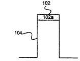
图1a至图1d表示根据一个实施例用于处理具有非平面表面的基底的一系列步骤。Figures 1a to 1d illustrate a series of steps for processing a substrate with a non-planar surface according to one embodiment.
图2为显示含有停止1.5keV植入所需的As的膜的厚度的图表。Figure 2 is a graph showing the thickness of a film containing As required to stop a 1.5keV implant.
图3为显示氧处理对AsH3植入的保留剂量的影响的图表。Figure 3 is a graph showing the effect of oxygen treatment on the retained dose ofAsH3 implants.
图4为显示保留剂量及串联电阻对AsH3植入的剂量之间的关系的图表。Figure 4 is a graph showing the relationship between retained dose and series resistance versus dose forAsH3 implants.
图5为显示保留剂量及串联电阻对AsH2植入的剂量之间的关系的图表。Figure 5 is a graph showing the relationship between retained dose and series resistance versus dose forAsH2 implants.
图6表示根据一个实施例用于处理基底的系统。Figure 6 illustrates a system for processing a substrate according to one embodiment.
图7表示根据第二实施例用于处理基底的系统。Fig. 7 shows a system for processing a substrate according to a second embodiment.
具体实施方式Detailed ways
在本发明中,介绍用于处理具有非平面表面的基底的新颖技术的若干实施例。出于清楚及简明的目的,将在一系统及制程的上下文中描述实施例,在所述系统及制程中,在一或多种处理剂入射于基底上时处理所述基底。系统及制程的特定实例可包含基于等离子的系统及技术,其中所述处理剂包含带电粒子。本发明中的粒子可涉及基于亚原子、原子或分子的粒子,包含光子、声子、电子、质子、中子、离子、气团(gas cluster)等。本发明中不排除没有必要涉及等离子的系统及制程(例如,化学气相沉积(chemical vapor deposition,CVD)技术、原子层沉积(atomic layerdeposition,ALD)技术、分子束磊晶(molecular beam epitaxy,MBE)技术)。此外,本发明可同等地适用于基于其他粒子或其他类似于粒子的处理剂(包含中性粒子、光子及声子)的系统及技术,例如,基于雷射的系统及制程等。In this disclosure, several embodiments of novel techniques for processing substrates with non-planar surfaces are presented. For purposes of clarity and simplicity, embodiments will be described in the context of a system and process in which a substrate is treated while one or more treating agents are incident on the substrate. Particular examples of systems and processes may include plasma-based systems and techniques wherein the treatment agent includes charged particles. Particles in the present invention may relate to subatomic, atomic or molecular based particles, including photons, phonons, electrons, protons, neutrons, ions, gas clusters and the like. The present invention does not exclude systems and processes that do not necessarily involve plasma (for example, chemical vapor deposition (chemical vapor deposition, CVD) technology, atomic layer deposition (atomic layer deposition, ALD) technology, molecular beam epitaxy (molecular beam epitaxy, MBE) technology). In addition, the present invention is equally applicable to systems and technologies based on other particles or other particle-like processing agents (including neutral particles, photons, and phonons), such as laser-based systems and processes.
为了避免混淆,本发明将集中于基于等离子的制程,例如,等离子辅助型掺杂(plasma assisted doping,PLAD)或等离子浸没式离子植入(plasmaimmersion ion implantation,PIII)系统,或等离子增强型化学气相沉积系统(plasma enhanced chemical vapor deposition system,PECVD),及其执行系统。然而,本领域技术人员将认识到,本发明不限于此类基于等离子的系统及制程。另外,本发明将集中于具有多个表面区段的FinFET基底,其中所述表面区段中的一个经定向以与另一不同表面区段相比具有对朝基底导向的粒子的较大暴露。前一表面区段可经定向为横越(但不一定垂直)朝基底导向的粒子路径,使得所述表面区段具有对所述粒子的较大暴露。同时,后一表面区段可经定向为沿着(但不一定平行)粒子路径,使得后一表面区段具有对粒子的较小暴露。虽然本发明集中于FinFET基底,但本领域技术人员将认识到,本发明将同等地适用于具有以不同角度定向的表面区段的任何类型的基底。To avoid confusion, the present invention will focus on plasma-based processes, such as plasma assisted doping (PLAD) or plasma immersion ion implantation (PIII) systems, or plasma-enhanced chemical vapor phase Deposition system (plasma enhanced chemical vapor deposition system, PECVD), and its execution system. However, those skilled in the art will recognize that the present invention is not limited to such plasma-based systems and processes. Additionally, the present invention will focus on FinFET substrates having multiple surface segments, where one of the surface segments is oriented to have greater exposure to substrate-directed particles than a different surface segment. The preceding surface section may be oriented transversely (but not necessarily perpendicularly) to the particle path directed towards the substrate such that the surface section has greater exposure to the particles. At the same time, the latter surface section can be oriented along (but not necessarily parallel to) the particle path such that the latter surface section has less exposure to the particles. Although the present invention focuses on FinFET substrates, those skilled in the art will recognize that the present invention will be equally applicable to any type of substrate having surface segments oriented at different angles.
用于处理具有非平面表面的基底的方法Method for processing substrates with non-planar surfaces
参看图1a至图1d,显示根据本发明的一个实施例用于处理具有非平面表面的基底的方法。所述方法可包括第一至第三阶段。在一个实施例中,可循序地执行所述阶段,其中一个阶段仅在另一阶段完成的后执行。在另一实施例中,可同时执行所述阶段中的至少一些。又在另一实施例中,两个或两个以上阶段的至少一部分可同时发生。在一个实施例中,可指定所述阶段的次序。然而,在另一实施例中,可不指定所述阶段的次序,且可以任何次序执行所述阶段。Referring to Figures 1a-1d, a method for processing a substrate having a non-planar surface according to one embodiment of the present invention is shown. The method may comprise first to third stages. In one embodiment, the phases may be performed sequentially, with one phase being performed only after the other phase is complete. In another embodiment, at least some of the stages may be performed concurrently. In yet another embodiment, at least a portion of two or more stages may occur simultaneously. In one embodiment, the order of the stages can be specified. However, in another embodiment, the order of the stages may not be specified, and the stages may be performed in any order.
在第一阶段期间,可优先处理基底100的第一区。本文中,第一表面区段可为具有对入射于基底上的粒子或处理剂的最高暴露的表面区段。在粒子以垂直于或实质上垂直于基底的角度入射的一个实施例中,所述第一表面区段可为水平延伸区段102,且第一区102a可为水平延伸区段102下方的区域。同时,第二表面区段可为垂直延伸区段104,且第二区可为邻近于垂直延伸区段104的区域104a。在另一实施例中,第一表面区段可为垂直延伸区段104,且第一区可为邻近于垂直延伸区段104的区域104a。同时,第二表面区段可为水平延伸区段102,且第二区可为水平延伸区段102下方的区域102a。出于清楚及简明的目的,将在前一实施例的上下文中描述所述方法。因此,本文中的第一表面区段可指代水平延伸表面区段,且水平延伸表面区段下方的区域将被称作第一区。During the first stage, a first region of the
在一个实施例中,可在第一阶段期间执行的制程可为掺杂制程。另外,可例如经由离子植入制程执行所述掺杂。在执行所述掺杂制程中,如图1b中所示,可用掺杂剂植入第一区102a,直至达成所要掺杂剂程度为止。在本发明中,所要掺杂剂程度可处于约1×10⁵掺杂剂/cm2至约1×1030掺杂剂/cm2的范围中。另外,可以所要深度植入第一区102a。所植入的粒子的能量可处于约5KeV至约15KeV的范围中。若诸如PLAD系统的基于等离子的系统用于执行第一阶段,则可藉由调整施加至基底的偏压来控制所要掺杂剂深度。若使用诸如束线离子植入系统(beam-line ionimplantation system)的系统,则可藉由调整朝基底导向的粒子的加速或减速来控制掺杂剂深度。亦可藉由经由例如退火制程调整基底的温度来控制掺杂剂深度。In one embodiment, the process that may be performed during the first phase may be a doping process. In addition, the doping may be performed, for example, via an ion implantation process. In performing the doping process, as shown in FIG. 1b, the
在某些实施例中,与第二表面区段104及第二区104a相比,第一阶段可更完全地处理第一表面区段102及第一区102a。举例而言,在掺杂制程中,可以所要剂量的掺杂剂植入第一区102a,而第二区104a可能接纳很少或不接纳所植入的掺杂剂。In some embodiments, the first stage may more completely treat the
本发明的方法亦可包括第二阶段。在一个实施例中,可在第一阶段的后执行第二阶段。在另一实施例中,可同时执行第一及第二阶段。又在另一实施例中,可在第一阶段之前执行第二阶段。在本实施例中,可在第二阶段期间执行的制程可为沉积制程。然而,在另一实施例中,第二制程技术可为另一不同类型的制程。在第二阶段期间,如图1c中所示,可在第一表面区段102上形成薄的膜106。尽管亦可在第二表面区段104上形成薄的膜108,但膜108形成于第二表面区段104上的速率可小于膜106形成于第一表面区段102上的速率。因此,若膜106及108分别形成于第一区段102及第二区段104两者上,则形成于第一区段102上的膜106可比形成于第二区段104上的膜厚。第二阶段可继续,直至形成于第一表面区段102上的膜106的厚度大于
如图2中所说明,可使用码TRIM计算含有停止1.5keV植入所需的As的膜的厚度。图2显示很少的离子穿透通过约
形成于第一表面区段102上的膜可含有第一阶段的掺杂剂中亦含有的物质。举例而言,第一阶段中所使用的掺杂剂及第二阶段期间所形成的膜可含有砷(As)、碳(C)、硼(B)、镓(Ga)、锗(Ge)、硅(Si)或其他金属或非金属材料。在另一实例中,第二阶段期间所形成的膜可不含有第一阶段期间所植入的掺杂剂中的物质。The film formed on the
若诸如PLAD或PECVD系统的基于等离子的系统用于执行第二阶段,则施加较低或较佳为零的偏压以促进膜的形成和/或阻碍将带电粒子植入至基底中。另外,等离子参数可经调整以控制形成于第一表面区段102及第二表面区段104上的膜的厚度的比率。举例而言,可调整等离子密度及反应速率。可藉由增加施加至等离子源的功率来调整等离子密度。可在第11/771,190号、第12/098,781号及第12/105,761号共同待决申请案中找到调整等离子密度的详细描述,所述申请案中的每一个全文以引用的方式并入本文中。同时,可藉由增加施加至等离子源的RF功率,或替代地藉由增加引入至系统的膜前驱体(film precursor)的浓度,来调整反应速率。If a plasma-based system such as a PLAD or PECVD system is used to perform the second stage, a lower or preferably zero bias is applied to facilitate film formation and/or hinder implantation of charged particles into the substrate. Additionally, plasma parameters can be adjusted to control the ratio of the thickness of the film formed on the
本发明的方法亦可包括第三阶段。在第三阶段中,优先处理其上尚未形成膜或其上形成具有较小厚度的膜的第二表面区段104。在本实施例中,第三阶段可与第一阶段相同或类似于第一阶段。由此,若第一阶段例如为植入制程,则第三阶段亦可为植入制程。另外,在第一及第三阶段期间所植入的掺杂剂可含有相同或不同物质。The method of the invention may also include a third stage. In the third stage, the
当粒子入射于第二表面区段104上时,处理区域104a。同时,形成于第一表面区段102上的膜106可防止或替代地限制表面区段102及第一区102a受到进一步处理。因此,可防止第一表面区段102及第一区102a被以粒子植入且经处理。或者,可以比植入第二表面区段104的速率低得多的速率以掺杂剂植入第一表面区段102。藉由用膜防止或限制第一表面区段102上的粒子植入,且促进第二表面区段104及第二区104a上的粒子植入,可避免或校正掺杂剂程度、植入深度或在不同表面区段间原本将发生的其他结果的较广变化。When particles are incident on the
本发明中所描述的方法可具有可选的化学或等离子处置阶段。在所述可选阶段期间,沉积于一或多个表面区段上的膜可暴露于含有氧的原子、分子或等离子(例如,O2、O3、H2O),且所述膜可被氧化。或者,所述膜可暴露于含有氮的原子、分子或等离子(例如,N2或NH3),且致使膜的氮化。又在另一实例中,所述膜可暴露于另一气态物质且与所述气态物质起化学反应。藉由对所述膜进行改质,可减少沉积于基底上的材料的挥发性(volatility)。另外,可在所述阶段期间对所述膜进行化学改质,以改良可溶性(solubility)且可进行植入后剥离(post implant stripping)。在图3中给出O2等离子处置及其对As保留剂量及植入分布的影响的实例。在此实例中,As的浓度在暴露于氧处置10秒后在几乎所有深度处增加。The methods described in this invention may have an optional chemical or plasma treatment stage. During the optional stage, the film deposited on one or more surface segments may be exposed to oxygen-containing atoms, molecules, or plasma (e.g.,O2 ,O3 ,H2O ), and the film may Oxidized. Alternatively, the film can be exposed to atoms, molecules or plasmas containing nitrogen (eg,N2 orNH3 ) and cause nitridation of the film. In yet another example, the film can be exposed to and chemically react with another gaseous species. By modifying the film, the volatility of the material deposited on the substrate can be reduced. Additionally, the membrane can be chemically modified during this stage to improve solubility and allow for post implant stripping. An example ofO2 plasma treatment and its effect on As retention dose and implant profile is given in Fig. 3. In this example, the concentration of As increased at almost all depths after exposure to oxygen treatment for 10 seconds.
在本实施例中,第一至第三阶段以及可选改质阶段的制程条件及参数可不同。如上文所述,较佳在第二阶段期间避免粒子的植入。然而,在第三阶段期间,最小程度的沉积或溅镀为较佳。在此阶段期间沉积膜可防止在所要表面区段处植入粒子。同时,溅镀可移除含有先前植入的掺杂剂的区域。在图4及图5中说明掺杂依据PLAD剂量而增加的制程的实例。在第一至第三阶段为基于等离子的制程的实施例中,包含施加至等离子源和/或基底的RF功率、能量、气体成分、稀释气体(diluent gas)、工作系数(duty factor)等的制程条件可经调整以将等离子掺杂制程置于所需机制(regime)的中心。在第11/771,190号、第12/098,781号、第12/105,761号及第11/376,522号共同待决申请案中描述了多设定点RF产生器(multiset-point RF generator)和/或斜坡电压(ramped voltage)的使用,所述申请案中的每一个全文以引用的方式并入本文中。In this embodiment, the process conditions and parameters of the first to third stages and the optional modification stage may be different. As mentioned above, implantation of particles is preferably avoided during the second stage. However, minimal deposition or sputtering is preferred during the third stage. Depositing a film during this stage prevents implantation of particles at desired surface sections. At the same time, sputtering can remove regions containing previously implanted dopants. An example of a process in which doping is increased as a function of PLAD dose is illustrated in FIGS. 4 and 5 . In embodiments where the first through third stages are plasma-based processes, parameters including RF power, energy, gas composition, diluent gas, duty factor, etc. applied to the plasma source and/or substrate Process conditions can be adjusted to center the plasma doping process on the desired regime. Multiset-point RF generators and/or ramps are described in co-pending applications 11/771,190, 12/098,781, 12/105,761, and 11/376,522 The use of ramped voltage, each of which is incorporated herein by reference in its entirety.
在本发明中,每一阶段可继续,直至达成所要特性为止。在第一及第三阶段涉及掺杂剂植入且第二阶段涉及膜形成的实施例中,每一阶段可继续,直至达成所要的植入剂量或膜厚度为止。可藉由监视粒子剂量、由制程表征(process characterization)及校准所判定的制程时间或自基底本身或腔室所接收的信号(例如,光学信号)来侦测每一阶段的终点。In the present invention, each stage can continue until the desired properties are achieved. In embodiments where the first and third stages involve dopant implantation and the second stage involves film formation, each stage may continue until the desired implant dose or film thickness is achieved. The end of each stage can be detected by monitoring particle dose, process time as determined by process characterization and calibration, or signals (eg, optical signals) received from the substrate itself or the chamber.
上文所描述的制程顺序是例示性的制程顺序。视特定应用的要求而定,可改变上文所描述的步骤的次序。另外,可重复每一个别阶段,且可重复一组阶段。此外,可视应用及结构的几何形状而定调整制程条件,以达成最佳结果。The process sequence described above is an exemplary process sequence. Depending on the requirements of a particular application, the order of the steps described above may be altered. Additionally, each individual stage can be repeated, and a group of stages can be repeated. Furthermore, the process conditions can be adjusted depending on the application and the geometry of the structure to achieve the best results.
举例而言,用于处理具有非平面表面的基底的方法可用于有效地掺杂动态随机存取存储器(dynamic random access memory,DRAM)电容器结构的沟槽。在此实例中,所述沟槽可具有100nm开口及4000nm深度的尺寸。为了掺杂所述沟槽,可以较高植入能量(例如,大于等于10kV)以As对所述结构进行植入。此例示性实施例中所使用的系统可为PLAD系统或束线离子植入器。在第一阶段期间,具有足够植入能量的离子可以浅角(shallow angle)入射于沟槽壁上。入射于沟槽上的壁上的离子的一部分可自表面弹起,且可均一地掺杂沟槽的整个深度。在可选的化学或等离子处置阶段期间,所述膜可暴露于O2等离子。所述处置阶段可减小沉积于晶圆上的材料的挥发性,并促进后处理(post processing)。For example, methods for processing substrates with non-planar surfaces can be used to efficiently dope trenches for dynamic random access memory (DRAM) capacitor structures. In this example, the trench may have dimensions of 100 nm opening and 4000 nm depth. To dope the trenches, the structure may be implanted with As at a higher implant energy (eg, 10 kV or greater). The system used in this exemplary embodiment may be a PLAD system or a beamline ion implanter. During the first phase, ions with sufficient implantation energy can be incident on the trench walls at shallow angles. A portion of the ions incident on the walls of the trench can bounce off the surface and uniformly dope the entire depth of the trench. During an optional chemical or plasma treatment stage, the membrane can be exposed toO2 plasma. The handling stage reduces the volatility of materials deposited on the wafer and facilitates post processing.
例示性系统Exemplary system
参看图6,显示根据本发明的一个实施例用于处理具有非平面表面的基底的例示性系统。本文中所揭示的系统600可为独立系统。或者,系统600可为包含一或多个系统600、一或多个基底监视系统、一或多个其他类型的基底处理系统及用于在不同系统之间转移基底的一或多个转移系统的群集工具(cluster tool)的一部分。Referring to FIG. 6, an exemplary system for processing a substrate having a non-planar surface is shown in accordance with one embodiment of the present invention. The
系统600可包括处理腔室602,其通常能够与例如涡轮泵606、机械泵608以及其他必需的真空密封组件一起具有高真空基础压力(highvacuum base pressure)。在处理腔室602内可存在支撑至少一个基底603的平台610。平台610可装备有一或多个温度管理元件,以调整并维持基底603的温度。亦可适应(accommodate)基底603的倾斜或旋转,以将基底与背景磁场(background magnetic field)对准。偏压源620可电耦接至平台610,因此耦接至基底603,从而将偏压施加至基底603。可藉由提供连续或脉冲RF或DC电流来施加所述偏压。若偏压源620提供RF电流,则可在偏压源与平台610之间提供阻抗匹配网路(impedance matchingnetwork)(未图示)。在本实施例中,偏压源620能够在操作期间调整并改变施加至基底603的偏压。举例而言,偏压源620可在操作期间连续地或步进地斜坡升高或降低施加至基底603的偏压。
处理腔室602亦可装备有一或多个原位(in situ)监视系统。举例而言,处理系统602中可包含一或多个温度监视系统,以监视基底的温度和/或环境温度。腔室602亦可装备有磁场监视系统(未图示),其能够监视背景磁场和/或制程完整性。The
系统600亦可包括等离子腔室604,其可与处理腔室602耦接或与处理腔室602间隔开,因此远离处理腔室602。等离子腔室亦可包含等离子源612,以用于产生高或低密度等离子。举例而言,等离子腔室604可包含感应耦接等离子(inductively coupled plasma,ICP)源、电容耦接等离子(capacitively coupled plasma,CCP)源、微波(microwave,MW)源、辉光放电(glow-discharge,GD)源、螺旋波(helicon)源或其组合。若等离子腔室604装备有ICP源,则系统600可包括平面及螺旋形线圈612a及612b中的至少一个、电耦接至线圈612a及612b中的一个或两者的电源612c以及阻抗匹配网路612d。若系统600装备有CCP源,则系统600可包括至少一个电极(未图示),其经定位以使得基底602界于所述电极与平台610之间。亦可包含电源612c,以将电极及平台610电耦接。此外,电源612c可耦接至阻抗匹配网路612d。若系统600装备有GD源,则系统600可包括至少一个电极(未图示),其经定位以使得基底602界于所述电极与平台610之间。另外,电源612可电耦接至电极及平台610。The
视等离子源612的类型而定,所述电源可为RF电源或DC电源。举例而言,若等离子源612为ICP或CCP源,则电源可为RF电源。然而,若等离子源612为GD源,则电源612可为DC源。若等离子源为CCP源,则电源612c可提供处于30至200MHz的范围中的高频RF电流。然而,亦可使用具有其他频率的RF电流。若等离子源612为ICP源,则由电源612c提供的RF电流可为处于1至30MHz的范围中的RF电流。然而,亦可使用具有其他频率的RF电流。若等离子源612为MW源,则RF电流可处于.3至300GHz的范围中。然而,亦可使用具有其他频率的RF电流。电源612可提供连续或脉冲电流。可在第10/905,172号共同待决申请案中找到对具有ICP等离子源的系统的详细描述,所述申请案全文以引用的方式并入本文中。Depending on the type of
在一个实施例中,将功率提供至等离子源(例如,线圈或电极)的电源612c亦可为将偏压提供至平台610的偏压源。举例而言,系统600可包括用以启动(activate)平台以及多个线圈(或电极)中的至少一个的单一电源。然而,系统600可较佳包括两个或两个以上电源,至少一个电源启动等离子源的线圈或电极,且至少一个另一电源启动处理腔室的平台。In one embodiment, the
系统600亦可包含一或多个处理气体源614及一或多个稀释气体源616。在本发明中,处理气体源614可含有包含硼(B)、磷或As的物质。处理气体源614可含有其他物质。一或多个稀释剂源616可含有包含氦、氖、氩、氪、氙、氡、氧、氮或其他气体的物质。
如上文所述,本文中所描述的系统600可为独立系统600。或者,系统600可为含有一或多个处理和/或监视系统的群集工具的一部分。若系统600为群集工具的一部分,则所述群集工具可包含转移机构,其用以将基底转移至各种处理和/或监视系统及自各种处理和/或监视系统转移基底,以在不将基底引入至开放大气的情况下循序地执行各种制程。As noted above, the
参看图7,显示根据本发明的一个实施例用于处理具有非平面表面的基底的例示性系统。在此实施例中,显示束线离子植入器。所述离子植入器可包含用于产生离子的离子源702。离子植入器700亦可包括一系列束线组件,离子束706通过所述束线组件。束线组件的实例可包含萃取电极704、磁质量分析器(magnetic mass analyzer)706、多个透镜708、束平行化器(beam parallelizer)710及加速/减速平台712。离子植入器700亦可包含支撑待植入的晶圆714的平台716。同时,可藉由一组件(有时称作“转板(roplat)”)(未图示)使晶圆714在一或多个维度上移动(例如,平移、旋转及倾斜)。Referring to FIG. 7, an exemplary system for processing a substrate having a non-planar surface is shown in accordance with one embodiment of the present invention. In this example, a beamline ion implanter is shown. The ion implanter may include an
在植入期间,自离子源702产生及萃取诸如氢离子的所要物质的离子。其后,所萃取的离子707沿着束线组件以束状状态行进并植入至晶圆714。非常类似于操纵光束的一系列光学透镜,束线组件操纵离子束707。由束线组件操纵的离子束707被引导。During implantation, ions of a desired species, such as hydrogen ions, are generated and extracted from
揭示一种用于处理具有非平面表面的基底的新颖方法及系统。如上文所述,所述系统及方法可适用于制造或处理各种类型的基底(包含FinFET或DRAM)。虽然本文已在出于特定目的特定实施于特定环境中的特定实施例的上下文中描述了本发明,但本领域技术人员将认识到,其有效性不限于此且本发明可出于任何数目的目的有益地实施于任何数目的环境中。在不脱离本文中所界定的本发明的精神及范畴的情况下,可作出形式及细节上的各种改变。因此,应依据本文中所描述的本发明的全部广度及精神来解释下文所陈述的申请专利范围。A novel method and system for processing substrates with non-planar surfaces is disclosed. As noted above, the systems and methods are applicable to fabricating or processing various types of substrates, including FinFETs or DRAMs. Although the invention has been described herein in the context of a particular embodiment for a particular purpose and in a particular environment, those skilled in the art will recognize that its effectiveness is not limited thereto and that the invention may be implemented in any number of ways. Purposes are beneficially implemented in any number of environments. Various changes in form and details may be made without departing from the spirit and scope of the invention as defined herein. Accordingly, the claims set forth below should be construed in light of the full breadth and spirit of the invention described herein.
Claims (17)
Applications Claiming Priority (5)
| Application Number | Priority Date | Filing Date | Title |
|---|---|---|---|
| US17236509P | 2009-04-24 | 2009-04-24 | |
| US61/172,365 | 2009-04-24 | ||
| US12/765,346US8202792B2 (en) | 2009-04-24 | 2010-04-22 | Method of processing a substrate having a non-planar surface |
| US12/765,346 | 2010-04-22 | ||
| PCT/US2010/032247WO2010124213A2 (en) | 2009-04-24 | 2010-04-23 | A method for processing a substrate having a non-planar substrate surface |
Publications (2)
| Publication Number | Publication Date |
|---|---|
| CN102449731Atrue CN102449731A (en) | 2012-05-09 |
| CN102449731B CN102449731B (en) | 2014-10-08 |
Family
ID=42992520
Family Applications (1)
| Application Number | Title | Priority Date | Filing Date |
|---|---|---|---|
| CN201080023330.2AActiveCN102449731B (en) | 2009-04-24 | 2010-04-23 | Substrate processing method with non-planar substrate surface |
Country Status (6)
| Country | Link |
|---|---|
| US (2) | US8202792B2 (en) |
| JP (1) | JP6074796B2 (en) |
| KR (1) | KR101626079B1 (en) |
| CN (1) | CN102449731B (en) |
| TW (1) | TWI543239B (en) |
| WO (1) | WO2010124213A2 (en) |
Families Citing this family (17)
| Publication number | Priority date | Publication date | Assignee | Title |
|---|---|---|---|---|
| JPH0735879A (en)* | 1993-07-22 | 1995-02-07 | Yukiro Kawashima | Radio wave clock outputting time, year, month and day signals |
| US8202792B2 (en)* | 2009-04-24 | 2012-06-19 | Varian Semiconductor Equipment Associates, Inc. | Method of processing a substrate having a non-planar surface |
| US20110039034A1 (en)* | 2009-08-11 | 2011-02-17 | Helen Maynard | Pulsed deposition and recrystallization and tandem solar cell design utilizing crystallized/amorphous material |
| US8679960B2 (en)* | 2009-10-14 | 2014-03-25 | Varian Semiconductor Equipment Associates, Inc. | Technique for processing a substrate having a non-planar surface |
| US8598020B2 (en)* | 2010-06-25 | 2013-12-03 | Applied Materials, Inc. | Plasma-enhanced chemical vapor deposition of crystalline germanium |
| US8664027B2 (en) | 2011-02-11 | 2014-03-04 | Varian Semiconductor Associates, Inc. | LED mesa sidewall isolation by ion implantation |
| US8501605B2 (en)* | 2011-03-14 | 2013-08-06 | Applied Materials, Inc. | Methods and apparatus for conformal doping |
| US9006065B2 (en)* | 2012-10-09 | 2015-04-14 | Advanced Ion Beam Technology, Inc. | Plasma doping a non-planar semiconductor device |
| JP6629312B2 (en) | 2014-07-03 | 2020-01-15 | アプライド マテリアルズ インコーポレイテッドApplied Materials,Incorporated | Method and apparatus for selective deposition |
| KR102252647B1 (en) | 2014-07-11 | 2021-05-17 | 삼성전자주식회사 | Pixel of an image sensor and image sensor |
| CN106033715B (en)* | 2015-03-11 | 2019-03-22 | 上海临港凯世通半导体有限公司 | The doping method of FinFET |
| CN106033728B (en)* | 2015-03-11 | 2019-07-09 | 上海凯世通半导体股份有限公司 | The doping method of FinFET |
| CN106033729B (en)* | 2015-03-11 | 2019-04-02 | 上海凯世通半导体股份有限公司 | The doping method of FinFET |
| CN106548958B (en)* | 2015-09-18 | 2020-09-04 | 中微半导体设备(上海)股份有限公司 | Integrated multifunctional cavity and substrate processing system |
| CN107437506B (en)* | 2016-05-27 | 2020-08-07 | 中芯国际集成电路制造(上海)有限公司 | Method for forming semiconductor structure |
| US10566242B2 (en)* | 2016-12-13 | 2020-02-18 | Taiwan Semiconductor Manufacturing Company, Ltd. | Minimization of plasma doping induced fin height loss |
| US10147584B2 (en) | 2017-03-20 | 2018-12-04 | Varian Semiconductor Equipment Associates, Inc. | Apparatus and techniques for decelerated ion beam with no energy contamination |
Citations (3)
| Publication number | Priority date | Publication date | Assignee | Title |
|---|---|---|---|---|
| US5512506A (en)* | 1995-04-06 | 1996-04-30 | Advanced Micro Devices, Inc. | Lightly doped drain profile optimization with high energy implants |
| US5888880A (en)* | 1996-10-30 | 1999-03-30 | Advanced Micro Devices, Inc. | Trench transistor with localized source/drain regions implanted through selectively grown oxide layer |
| US20060240636A1 (en)* | 2005-02-21 | 2006-10-26 | Ryu Hyuk-Ju | Trench isolation methods of semiconductor device |
Family Cites Families (12)
| Publication number | Priority date | Publication date | Assignee | Title |
|---|---|---|---|---|
| US5874346A (en) | 1996-05-23 | 1999-02-23 | Advanced Micro Devices, Inc. | Subtrench conductor formation with large tilt angle implant |
| KR100266006B1 (en) | 1997-09-10 | 2000-09-15 | 김영환 | Impurity-doped thin film formation method |
| US5998267A (en) | 1998-09-18 | 1999-12-07 | National Semiconductor Corporation | Process to manufacture high density ULSI ROM array |
| JP3652322B2 (en)* | 2002-04-30 | 2005-05-25 | Necエレクトロニクス株式会社 | Vertical MOSFET and manufacturing method thereof |
| JP2006121019A (en)* | 2004-09-22 | 2006-05-11 | Hitachi Kokusai Electric Inc | Manufacturing method of semiconductor device |
| JP2006128380A (en)* | 2004-10-28 | 2006-05-18 | Toshiba Corp | Semiconductor device manufacturing method and manufacturing apparatus |
| KR100694471B1 (en) | 2005-08-24 | 2007-03-12 | 매그나칩 반도체 유한회사 | Manufacturing method of image sensor to improve optical characteristics |
| EP1892765A1 (en)* | 2006-08-23 | 2008-02-27 | INTERUNIVERSITAIR MICROELEKTRONICA CENTRUM vzw (IMEC) | Method for doping a fin-based semiconductor device |
| EP2073256A1 (en)* | 2007-12-20 | 2009-06-24 | Interuniversitair Microelektronica Centrum vzw ( IMEC) | Method for fabricating a semiconductor device and the semiconductor device made thereof |
| US8202792B2 (en)* | 2009-04-24 | 2012-06-19 | Varian Semiconductor Equipment Associates, Inc. | Method of processing a substrate having a non-planar surface |
| US8298925B2 (en)* | 2010-11-08 | 2012-10-30 | Taiwan Semiconductor Manufacturing Company, Ltd. | Mechanisms for forming ultra shallow junction |
| US8039349B2 (en)* | 2009-07-30 | 2011-10-18 | Globalfoundries Inc. | Methods for fabricating non-planar semiconductor devices having stress memory |
- 2010
- 2010-04-22USUS12/765,346patent/US8202792B2/enactiveActive
- 2010-04-23WOPCT/US2010/032247patent/WO2010124213A2/enactiveApplication Filing
- 2010-04-23JPJP2012507434Apatent/JP6074796B2/enactiveActive
- 2010-04-23TWTW099112847Apatent/TWI543239B/enactive
- 2010-04-23KRKR1020117027406Apatent/KR101626079B1/enactiveActive
- 2010-04-23CNCN201080023330.2Apatent/CN102449731B/enactiveActive
- 2012
- 2012-05-24USUS13/480,204patent/US8507372B2/enactiveActive
Patent Citations (3)
| Publication number | Priority date | Publication date | Assignee | Title |
|---|---|---|---|---|
| US5512506A (en)* | 1995-04-06 | 1996-04-30 | Advanced Micro Devices, Inc. | Lightly doped drain profile optimization with high energy implants |
| US5888880A (en)* | 1996-10-30 | 1999-03-30 | Advanced Micro Devices, Inc. | Trench transistor with localized source/drain regions implanted through selectively grown oxide layer |
| US20060240636A1 (en)* | 2005-02-21 | 2006-10-26 | Ryu Hyuk-Ju | Trench isolation methods of semiconductor device |
Also Published As
| Publication number | Publication date |
|---|---|
| JP2012525011A (en) | 2012-10-18 |
| JP6074796B2 (en) | 2017-02-08 |
| KR101626079B1 (en) | 2016-05-31 |
| US8202792B2 (en) | 2012-06-19 |
| WO2010124213A2 (en) | 2010-10-28 |
| US20100273322A1 (en) | 2010-10-28 |
| WO2010124213A3 (en) | 2011-01-20 |
| US8507372B2 (en) | 2013-08-13 |
| TWI543239B (en) | 2016-07-21 |
| TW201216332A (en) | 2012-04-16 |
| KR20120006550A (en) | 2012-01-18 |
| CN102449731B (en) | 2014-10-08 |
| US20120295430A1 (en) | 2012-11-22 |
Similar Documents
| Publication | Publication Date | Title |
|---|---|---|
| CN102449731B (en) | Substrate processing method with non-planar substrate surface | |
| US5354698A (en) | Hydrogen reduction method for removing contaminants in a semiconductor ion implantation process | |
| US7989329B2 (en) | Removal of surface dopants from a substrate | |
| TWI620233B (en) | Method and apparatus for selective deposition | |
| US8501605B2 (en) | Methods and apparatus for conformal doping | |
| CN102598219B (en) | Method for processing substrates with non-planar surfaces | |
| US20100297854A1 (en) | High throughput selective oxidation of silicon and polysilicon using plasma at room temperature | |
| WO2006083778A2 (en) | Selective plasma re-oxidation process using pulsed rf source power | |
| WO2006083858A2 (en) | Plasma gate oxidation process using pulsed rf source power | |
| JP5558480B2 (en) | Improvement of conformal doping in P3i chamber | |
| US20080011426A1 (en) | Plasma reactor with inductively coupled source power applicator and a high temperature heated workpiece support | |
| JP2012507867A (en) | Adjustment of doping profile in P3i process | |
| US20120302048A1 (en) | Pre or post-implant plasma treatment for plasma immersed ion implantation process |
Legal Events
| Date | Code | Title | Description |
|---|---|---|---|
| C06 | Publication | ||
| PB01 | Publication | ||
| C10 | Entry into substantive examination | ||
| SE01 | Entry into force of request for substantive examination | ||
| C14 | Grant of patent or utility model | ||
| GR01 | Patent grant |