CN102449582A - Capacitance type input device - Google Patents
Capacitance type input deviceDownload PDFInfo
- Publication number
- CN102449582A CN102449582ACN2010800232259ACN201080023225ACN102449582ACN 102449582 ACN102449582 ACN 102449582ACN 2010800232259 ACN2010800232259 ACN 2010800232259ACN 201080023225 ACN201080023225 ACN 201080023225ACN 102449582 ACN102449582 ACN 102449582A
- Authority
- CN
- China
- Prior art keywords
- light
- insulating film
- transmitting electrodes
- input device
- transmitting
- Prior art date
- Legal status (The legal status is an assumption and is not a legal conclusion. Google has not performed a legal analysis and makes no representation as to the accuracy of the status listed.)
- Granted
Links
Images


Classifications
- G—PHYSICS
- G06—COMPUTING OR CALCULATING; COUNTING
- G06F—ELECTRIC DIGITAL DATA PROCESSING
- G06F3/00—Input arrangements for transferring data to be processed into a form capable of being handled by the computer; Output arrangements for transferring data from processing unit to output unit, e.g. interface arrangements
- G06F3/01—Input arrangements or combined input and output arrangements for interaction between user and computer
- G06F3/03—Arrangements for converting the position or the displacement of a member into a coded form
- G06F3/041—Digitisers, e.g. for touch screens or touch pads, characterised by the transducing means
- G06F3/044—Digitisers, e.g. for touch screens or touch pads, characterised by the transducing means by capacitive means
- G06F3/0443—Digitisers, e.g. for touch screens or touch pads, characterised by the transducing means by capacitive means using a single layer of sensing electrodes
- G—PHYSICS
- G06—COMPUTING OR CALCULATING; COUNTING
- G06F—ELECTRIC DIGITAL DATA PROCESSING
- G06F3/00—Input arrangements for transferring data to be processed into a form capable of being handled by the computer; Output arrangements for transferring data from processing unit to output unit, e.g. interface arrangements
- G06F3/01—Input arrangements or combined input and output arrangements for interaction between user and computer
- G06F3/03—Arrangements for converting the position or the displacement of a member into a coded form
- G06F3/041—Digitisers, e.g. for touch screens or touch pads, characterised by the transducing means
- G06F3/044—Digitisers, e.g. for touch screens or touch pads, characterised by the transducing means by capacitive means
- G06F3/0446—Digitisers, e.g. for touch screens or touch pads, characterised by the transducing means by capacitive means using a grid-like structure of electrodes in at least two directions, e.g. using row and column electrodes
- H—ELECTRICITY
- H03—ELECTRONIC CIRCUITRY
- H03K—PULSE TECHNIQUE
- H03K17/00—Electronic switching or gating, i.e. not by contact-making and –breaking
- H03K17/94—Electronic switching or gating, i.e. not by contact-making and –breaking characterised by the way in which the control signals are generated
- H03K17/96—Touch switches
- H03K17/962—Capacitive touch switches
- H03K17/9622—Capacitive touch switches using a plurality of detectors, e.g. keyboard
- G—PHYSICS
- G06—COMPUTING OR CALCULATING; COUNTING
- G06F—ELECTRIC DIGITAL DATA PROCESSING
- G06F2203/00—Indexing scheme relating to G06F3/00 - G06F3/048
- G06F2203/041—Indexing scheme relating to G06F3/041 - G06F3/045
- G06F2203/04111—Cross over in capacitive digitiser, i.e. details of structures for connecting electrodes of the sensing pattern where the connections cross each other, e.g. bridge structures comprising an insulating layer, or vias through substrate
- H—ELECTRICITY
- H03—ELECTRONIC CIRCUITRY
- H03K—PULSE TECHNIQUE
- H03K2217/00—Indexing scheme related to electronic switching or gating, i.e. not by contact-making or -breaking covered by H03K17/00
- H03K2217/94—Indexing scheme related to electronic switching or gating, i.e. not by contact-making or -breaking covered by H03K17/00 characterised by the way in which the control signal is generated
- H03K2217/96—Touch switches
- H03K2217/96042—Touch switches with illumination
- H—ELECTRICITY
- H03—ELECTRONIC CIRCUITRY
- H03K—PULSE TECHNIQUE
- H03K2217/00—Indexing scheme related to electronic switching or gating, i.e. not by contact-making or -breaking covered by H03K17/00
- H03K2217/94—Indexing scheme related to electronic switching or gating, i.e. not by contact-making or -breaking covered by H03K17/00 characterised by the way in which the control signal is generated
- H03K2217/96—Touch switches
- H03K2217/9607—Capacitive touch switches
- H03K2217/960755—Constructional details of capacitive touch and proximity switches
Landscapes
- Engineering & Computer Science (AREA)
- General Engineering & Computer Science (AREA)
- Theoretical Computer Science (AREA)
- Human Computer Interaction (AREA)
- Physics & Mathematics (AREA)
- General Physics & Mathematics (AREA)
- Position Input By Displaying (AREA)
- Electronic Switches (AREA)
Abstract
Description
Translated fromChinese技术领域technical field
本发明涉及一种静电容量方式输入装置,该静电容量方式输入装置具备排列于同一层的多个透光电极,并能检测出手指等所接触的电极的位置。The present invention relates to an electrostatic capacitance type input device, which is provided with a plurality of light-transmitting electrodes arranged on the same layer, and capable of detecting the position of the electrodes touched by a finger or the like.
背景技术Background technique
近年来,移动电话、便携式信息终端、车辆导航系统等各种电子设备的操作部都开始采用触摸面板。触摸面板通过在液晶面板等显示装置的显示画面上贴上可检测出手指等所接触的位置的输入装置而构成。构成触摸面板的输入装置根据构造及检测方式的不同,有电阻膜方式或静电容量方式等各种类型。其中,静电容量方式输入装置在1片基板上具有透光性导电膜(透光电极),通过检测经由静电容量(通过手指等触碰而形成)流动的微弱电流量的变化来确定所接触的位置,与电阻膜方式输入装置相比,具有可获得更高透射率的优点。In recent years, touch panels have been used in the operation sections of various electronic devices such as mobile phones, portable information terminals, and car navigation systems. The touch panel is configured by affixing an input device capable of detecting a position touched by a finger or the like on a display screen of a display device such as a liquid crystal panel. There are various types of input devices constituting a touch panel, such as a resistive film type or an electrostatic capacitance type, depending on the structure and detection method. Among them, the capacitive input device has a light-transmitting conductive film (light-transmitting electrode) on a single substrate, and determines the contact by detecting changes in the amount of weak current flowing through the electrostatic capacity (formed by touching with a finger, etc.). Position, compared with the resistance film type input device, there is an advantage that higher transmittance can be obtained.
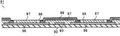
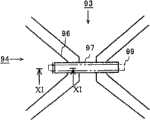
图6是表示专利文献一所记载的现有静电容量方式输入装置的概要结构的俯视图,图7是图6所示的VII-VII线的放大截面图。6 is a plan view showing a schematic configuration of a conventional capacitive input device described in
静电容量方式输入装置91在基板92上具备沿X轴方向(图的上下方向)延伸的多个X轴轨迹(trace)93、以及沿Y轴方向(图的左右方向)延伸且与X轴轨迹93交叉配置的多个Y轴轨迹(trace)94,并分别检测X轴方向及Y轴方向的手指等的接触位置。The
X轴轨迹93通过使排列在X轴方向上的多个透明电极95相互连结而形成。另一方面,Y轴轨迹94通过使间歇地配置在Y轴方向上的多个透明电极96经由由导电性材料构成的跳线(jumper)99电连接而形成。跳线99跨越一部分X轴轨迹(相邻的一对透明电极95的连结部分)的上方,而形成于层叠在X轴轨迹93及Y轴轨迹94上的绝缘膜97上,并并经由位于透明电极96上的通孔98而与透明电极96连接。The
这样,专利文献一记载的结构中,为了使X轴轨迹93与跨越该X轴轨迹93而形成的跳线99之间绝缘,而在基板92的整面上形成绝缘膜,并仅在跳线99与透明电极96之间的连接位置设置通孔98。In this way, in the structure described in
此外,专利文献二记载了仅在跳线所跨越的部分形成绝缘膜的结构,来取代在基板92的整面设置绝缘膜的结构。In addition,
上述现有的静电容量方式输入装置通过在基板上依次层叠透光电极、绝缘膜、跳线(导电体)而形成。此情况下存在以下问题。The above-mentioned conventional capacitive input device is formed by sequentially stacking a light-transmitting electrode, an insulating film, and a jumper (conductor) on a substrate. In this case, the following problems exist.
第一,由于跳线形成于靠人的一侧(与液晶面板相反的一侧),所以在用具有金属光泽的导电材料来形成跳线的情况下,跳线看上去很显眼。First, since the jumper is formed on the side close to the person (the side opposite to the liquid crystal panel), the jumper looks conspicuous when the jumper is formed of a conductive material having metallic luster.
第二,在绝缘膜的一部分形成为突起(overhang)状态的情况下,跳线跨越突起部分的可能性高,容易导致跳线的断线。Second, when a part of the insulating film is formed in an overhang state, there is a high possibility that the jumper wire will straddle the overhang portion, which easily leads to disconnection of the jumper wire.
图8是说明图6所示的静电容量方式输入装置中绝缘膜产生突起的情况的俯视图。图9是图8所示的IX-IX线的截面图。FIG. 8 is a plan view illustrating a state in which a protrusion occurs on an insulating film in the capacitive input device shown in FIG. 6 . Fig. 9 is a cross-sectional view taken along line IX-IX shown in Fig. 8 .
通孔98是通过在基板92的整体上层叠绝缘膜97后,对该绝缘膜的一部分进行选择性蚀刻而形成。然而,若蚀刻的处理时间过长,则蚀刻会在距离绝缘膜97表面较深的部分进一步进行,如图9的截面图所示,就会有绝缘膜97的表面侧的部分成为朝向通孔98的中心侧突起的形状(overhang,突起)的情况。The
例如,若在图8所示的箭头所示的范围内产生突起,则如图9的双点划线所示那样,用于连接相邻的一对透明电极96的跳线99就会断线,从而无法获得Y轴轨迹94的导通状态。在此,假设在通孔的半周产生突起,则跳线99的形成区域与突起区域就会有50%左右的概率会重叠,由此可知产生断线的概率就变得更高。For example, if a protrusion occurs within the range indicated by the arrow shown in FIG. 8, the
图10是说明专利文献二所记载的现有的静电容量方式输入装置中,绝缘膜产生突起的情况的俯视图,图11为图10所示的XI-XI线的截面图。FIG. 10 is a plan view illustrating a state where the insulating film protrudes in the conventional capacitive input device described in
专利文献二所记载的、仅在跳线99跨越X轴轨迹93的部分设置绝缘膜97的结构也会产生同样的问题。例如,若在图10中箭头所示的范围(绝缘膜97的短边部分)产生突起,则如图11的双点划线所示那样,跳线99就会断线,从而Y轴轨迹94不导通。The structure described in
【专利文献1】:日本注册实用新型专利第3144563号公报[Patent Document 1]: Japanese Registered Utility Model Patent No. 3144563
【专利文献2】:日本注册实用新型专利第3144241号公报[Patent Document 2]: Japanese Registered Utility Model Patent No. 3144241
发明内容Contents of the invention
故而,本发明的目的在于提供一种在同一层排列双轴向的透光电极结构的静电容量方式输入装置,该输入装置具有互相连接一个轴向的透光电极的跳线不显眼,且断线的可能性低的结构。Therefore, the object of the present invention is to provide a capacitive input device in which biaxial light-transmitting electrodes are arranged on the same layer. A structure with a low possibility of a line.
本发明的静电容量方式输入装置具备:基板、多个导电体、绝缘膜、多个第1透光电极以及多个第2透光电极,多个导电体在基板上排列于第一方向及与该第一方向正交的第二方向上,绝缘膜形成为覆盖导电体及基板,多个第1透光电极在绝缘膜上排列于第一方向及第二方向上,多个第2透光电极在绝缘膜上排列于第一方向及第二方向上,并分别配置于第1透光电极的行列之间。排列于第一方向上的各个第1透光电极经由形成于绝缘膜的通孔,并通过导电体而互相电连接,排列于第二方向上的各个第2透光电极在绝缘膜上互相连接。The capacitive input device of the present invention includes: a substrate, a plurality of conductors, an insulating film, a plurality of first light-transmitting electrodes, and a plurality of second light-transmitting electrodes, and the plurality of conductors are arranged on the substrate in a first direction and In the second direction perpendicular to the first direction, the insulating film is formed to cover the conductor and the substrate, a plurality of first light-transmitting electrodes are arranged on the insulating film in the first direction and the second direction, and a plurality of second light-transmitting electrodes are arranged on the insulating film. The electrodes are arranged on the insulating film in the first direction and the second direction, and are respectively arranged between the rows and columns of the first light-transmitting electrodes. The first light-transmitting electrodes arranged in the first direction are electrically connected to each other through conductors through the through holes formed in the insulating film, and the second light-transmitting electrodes arranged in the second direction are connected to each other on the insulating film. .
此外,本发明的静电容量方式输入装置具备:基板、多个导电体、多个绝缘膜、多个第1透光电极以及多个第2透光电极,多个导电体在基板上排列于第一方向及与该第一方向正交的第二方向上,多个绝缘膜形成为局部地覆盖各个导电体,多个第1透光电极排列于第一方向及第二方向上,多个第2透光电极排列于第一方向及第二方向上,并分别配置于第1透光电极的行列之间。排列于第一方向的各个第1透光电极通过抵接导电体中未被绝缘膜覆盖的部分,从而通过导电体而互相电连接,排列于第二方向上的各个第2透光电极在绝缘膜上互相连接。In addition, the capacitive input device of the present invention includes: a substrate, a plurality of conductors, a plurality of insulating films, a plurality of first light-transmitting electrodes, and a plurality of second light-transmitting electrodes. In one direction and in a second direction perpendicular to the first direction, a plurality of insulating films are formed to partially cover each conductor, a plurality of first light-transmitting electrodes are arranged in the first direction and a second direction, and a plurality of first 2. The light-transmitting electrodes are arranged in the first direction and the second direction, and are respectively arranged between rows and columns of the first light-transmitting electrodes. Each of the first light-transmitting electrodes arranged in the first direction is electrically connected to each other through the conductor by contacting the part of the conductor not covered by the insulating film, and each of the second light-transmitting electrodes arranged in the second direction is insulated. connected to each other in the membrane.
(发明效果)(invention effect)
根据本发明,多个透光电极排列于同一层的静电容量方式输入装置中,由于用于使透光电极互相连接的导电体形成于基板上(即,输入装置的内部),因此能够使导电体变得不显眼。此外,通过将各个第1透光电极形成为覆盖导电体中未被绝缘膜覆盖的部分的整体,从而无论绝缘膜的截面形状如何,都能够防止导电体的断线。According to the present invention, in the capacitive input device in which a plurality of light-transmitting electrodes are arranged on the same layer, since the conductor for connecting the light-transmitting electrodes to each other is formed on the substrate (that is, inside the input device), it is possible to make the conduction body becomes inconspicuous. Furthermore, by forming each of the first light-transmitting electrodes so as to cover the entire portion of the conductor not covered by the insulating film, disconnection of the conductor can be prevented regardless of the cross-sectional shape of the insulating film.
此外,在透光电极覆盖通孔的整个开口部的情况下,即使绝缘膜在开口部的部分范围内产生突起,透光电极仍然可以沿无突起的通孔的内壁而到达导电体表面。因此,无论通孔内壁的截面形状如何,都能够防止导电体的断线。In addition, when the light-transmitting electrode covers the entire opening of the through-hole, even if the insulating film protrudes in a part of the opening, the light-transmitting electrode can still reach the surface of the conductor along the inner wall of the through-hole without protrusion. Therefore, regardless of the cross-sectional shape of the inner wall of the through-hole, disconnection of the conductor can be prevented.
并且,由于导电体中未被绝缘膜覆盖的一部分与透光电极能够实现面接触,因此即使由于蚀刻处理而在绝缘膜的外周壁产生突起的情况下,仍然能够确保透光电极与导电体之间的连接。And, since the part of the conductor not covered by the insulating film can be in surface contact with the light-transmitting electrode, even if a protrusion occurs on the outer peripheral wall of the insulating film due to etching, the gap between the light-transmitting electrode and the conductor can still be ensured. connection between.
附图说明Description of drawings
图1是表示本发明的第1实施方式的静电容量方式输入装置的概要结构的俯视图。FIG. 1 is a plan view showing a schematic configuration of a capacitive input device according to a first embodiment of the present invention.
图2是图1所示的II-II线的放大截面图。Fig. 2 is an enlarged sectional view taken along line II-II shown in Fig. 1 .
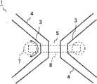
图3是图1所示的通孔附近的放大图。FIG. 3 is an enlarged view of the vicinity of a through hole shown in FIG. 1 .
图4是表示本发明的第2实施方式的静电容量方式输入装置的概要结构的俯视图。4 is a plan view showing a schematic configuration of a capacitive input device according to a second embodiment of the present invention.
图5是图4所示的V-V线的放大截面图。Fig. 5 is an enlarged sectional view taken along line V-V shown in Fig. 4 .
图6是表示现有的静电容量方式输入装置的概要结构的俯视图。6 is a plan view showing a schematic configuration of a conventional capacitive input device.
图7是图6所示的VII-VII线的放大截面图。Fig. 7 is an enlarged sectional view taken along line VII-VII shown in Fig. 6 .
图8是说明图6所示的静电容量方式输入装置中绝缘膜产生突起的情况的俯视图。FIG. 8 is a plan view illustrating a state in which a protrusion occurs on an insulating film in the capacitive input device shown in FIG. 6 .
图9是图8所示的IX-IX线的截面图。Fig. 9 is a cross-sectional view taken along line IX-IX shown in Fig. 8 .
图10是说明现有的静电容量方式输入装置中绝缘膜产生突起的情况的俯视图。FIG. 10 is a plan view illustrating a state in which protrusions are generated in an insulating film in a conventional capacitive input device.
图11是图10所示的XI-XI线的截面图。Fig. 11 is a cross-sectional view taken along line XI-XI shown in Fig. 10 .
(附图标记说明)(Description of Reference Signs)
1静电容量方式输入装置1 Capacitive input device
2基板2 substrates
3第1透光电极3 The first light-transmitting electrode
4第2透光电极4 The second light-transmitting electrode
6绝缘膜6 insulating film
7通孔7 through holes
8跳线8 jumpers
具体实施方式Detailed ways
(第1实施方式)(first embodiment)
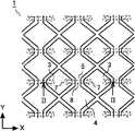
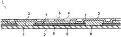
图1是表示本发明的第1实施方式的静电容量方式输入装置的概要结构的俯视图,图2是图1所示的II-II线的放大截面图。此外,图3是图1所示的通孔附近的放大图。1 is a plan view showing a schematic configuration of a capacitive input device according to a first embodiment of the present invention, and FIG. 2 is an enlarged cross-sectional view taken along line II-II shown in FIG. 1 . In addition, FIG. 3 is an enlarged view of the vicinity of the through hole shown in FIG. 1 .
静电容量方式输入装置1具备基板2、多个跳线8、绝缘膜6、多个第1透光电极3、以及多个第2透光电极4。跳线8、绝缘膜6、透光电极(第1透光电极3及第2透光电极4)按照上述顺序形成于基板2上。The
跳线8由具有导电性的材料形成,并在基板2的表面上排列成行列状。各跳线8分别用于在X轴方向上连接第1透光电极3,其两端部的位置及尺寸形成为分别与X轴方向上相邻的一对第1透光电极3互相重叠。跳线8例如可由ITO(Indium Tin Oxide:氧化铟锡)、Mo/Al/Mo的层叠体、Ag、Ag合金及导电性高分子形成。The
绝缘膜6是通过将绝缘材料层叠成覆盖跳线8及基板2的表面而形成,在第1透光电极3与跳线8互相重叠的部分设有到达跳线8的表面的通孔7。The insulating
第1透光电极3及第2透光电极4在同一层内,在X轴方向及与X轴方向正交的Y轴方向上排列成矩阵状。第1透光电极3及第2透光电极4在同一工序中使用ITO等透光性导电材料而形成。The first light-transmitting
如图1所示,在绝缘膜6上,各第1透光电极3在X轴方向及Y轴方向上都没有互相连接,而经由通孔7连接到基板2上的跳线8。其结果,排列于X轴方向上的第1透光电极3处于互相电连接的状态。As shown in FIG. 1 , on the insulating
另一方面,第2透光电极4分别配置于第1透光电极3的行列之间,并在绝缘膜6上,经由与第2透光电极4同时图案化的连接部5而在Y轴方向上相互连结。On the other hand, the second light-transmitting
在X轴方向上连接的第1透光电极3与Y轴方向上连接的第2透光电极4排列在同一层的情况下,由于会产生交叉部分,所以要在任意一个方向上进行连接就需要如跳线8这样的布线部。本实施方式的静电容量方式输入装置1中,跳线8形成在基板2的表面,并且在其上面形成有绝缘膜6、第1透光电极3及第2透光电极4,从而能够使跳线8在从表面侧观看时不显眼。When the first light-transmitting
本实施方式中,由于通孔7的整个开口部都被第1透光电极3覆盖,所以例如即使绝缘膜在图3所示的箭头的范围内产生突起(overhang)(参照图9)时,第1透光电极3仍然可以沿无突起的通孔7的内壁而到达跳线8的表面。因此,无论通孔7内壁的截面形状如何,都能够防止跳线8的断线。In the present embodiment, since the entire opening of the through
如上所述,跳线8可以由具有导电性的各种材料形成,而在使用具有遮光性的材料的情况下,还有以下优点。As described above, the
在由遮光性材料形成跳线8的情况下,在与跳线8的图案形成相同的工序,使用与跳线8相同的材料,能够在基板2上形成定位用的对准标记。其结果,不仅能够减少对准标记形成过程,而且不需要对用来形成第2层以后的膜的曝光机进行特别的改造,就能够使用标准的读取机构进行曝光时的定位。When the
此外,在形成第2层以后的膜时,通过显微镜等作目视确认来进行位置对准的情况下,由于第1层的跳线8由遮光性材料形成,所以辨识性得到提高,从而能够容易地进行定位。In addition, when forming the film of the second layer or later, in the case of visually confirming the position with a microscope or the like, since the
此外,也可以采用导电性高分子材料来作为遮光性材料。一般而言,高分子膜的透光性和导电性虽然是一种权衡(trade off)关系,但是只要是形成有跳线8的有限范围内,即使具有遮光性,对输入装置整体的光透射性造成的影响也较小。此外,对于导电性而言,只要是具有ITO般的电阻值的材料即可,所以可以利用生产性较高的导电性高分子。In addition, a conductive polymer material can also be used as the light-shielding material. Generally speaking, although the light transmittance and conductivity of the polymer film are a trade-off relationship, as long as the
在使用金属作为遮光性材料的情况下,由于可在1个工序中对跳线8、以及基板2上未图示的金属布线层(与透光电极连接的布线等)同时进行图案形成,因此能够减少工序数量,从而能够降低成本。In the case of using metal as the light-shielding material, the
(第2实施方式)(second embodiment)
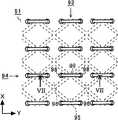
图4是表示本发明的第2实施方式的静电容量方式输入装置的概要结构的俯视图,图5是图4所示的V-V线的放大截面图。4 is a plan view showing a schematic configuration of a capacitive input device according to a second embodiment of the present invention, and FIG. 5 is an enlarged cross-sectional view taken along line V-V shown in FIG. 4 .
本实施方式的静电容量方式输入装置与第1实施方式同样地,通过在基板2上依次层叠跳线8、绝缘膜6、透光电极(第1透光电极3及第2透光电极4)而构成,但,绝缘膜6的形成区域与第1实施方式不同。以下,主要说明本实施方式与第1实施方式的不同之处。In the capacitive input device of this embodiment, similarly to the first embodiment, a
本实施方式中,仅在与使相邻的第2透光电极4连接的连接部5交叉的部分设有绝缘膜6。更详细而言,绝缘膜6形成为,局部地覆盖各跳线8,即,不覆盖其中跳线8与相邻的各第1透光电极3互相重叠的部分中的一部分(斜线部)。此外,本实施方式中,虽然在跳线8两边的端部设有未被绝缘膜6覆盖的部分,但未被绝缘膜6覆盖的区域并不一定要是端部,只要是跳线8与透光电极的重叠部分的一部分即可。In the present embodiment, the insulating
此外,各第1透光电极3形成为,覆盖跳线8的表面中未被绝缘膜6覆盖的一部分(斜线部)的整体,并抵接跳线8的该一部分。由此,排列在X轴方向上的第1透光电极3处于互相电连接的状态。另一方面,排列在Y轴方向上的各第2透光电极在覆盖跳线8的绝缘膜6上经由连接部5而连接。In addition, each first light-transmitting
本实施方式的静电容量方式输入装置1中,也是跳线8形成在基板2的表面,并且在其上面形成绝缘膜6、第1透光电极3及第2透光电极4,从而能够使跳线8在从表面侧观看时不显眼。In the
此外,本实施方式的静电容量方式输入装置1中,由于跳线8中未被绝缘膜6覆盖的一部分与第1透光电极3能够实现面接触,因此即使因蚀刻处理而如图5的截面所示那样产生突起(绝缘膜6的外周壁的截面中,绝缘膜6的表面侧的部分更往外侧突起的状态)时,也能够确保第1透光电极3与跳线8的连接。In addition, in the
此外,虽然上述各实施方式中说明了通过跳线来使透光电极在X轴方向上互相连接的例子,但也可以使图1的例子的X轴与Y轴相反,使X轴方向上的透光电极经由连接部而连接,使Y轴方向上的透光电极通过跳线而连接。In addition, although the examples in which the light-transmitting electrodes are connected to each other in the X-axis direction by jumping wires have been described in the above-mentioned embodiments, it is also possible to make the X-axis and the Y-axis of the example in FIG. The light-transmitting electrodes are connected through the connecting portion, and the light-transmitting electrodes in the Y-axis direction are connected by jumpers.
本发明可应用在构成用作各种电子设备的输出输入设备的触摸面板等。The present invention can be applied to a touch panel and the like constituting an input/output device of various electronic devices.
Claims (5)
Translated fromChineseApplications Claiming Priority (3)
| Application Number | Priority Date | Filing Date | Title |
|---|---|---|---|
| JP2009-129326 | 2009-05-28 | ||
| JP2009129326AJP5278759B2 (en) | 2009-05-28 | 2009-05-28 | Capacitive input device |
| PCT/JP2010/003540WO2010137316A1 (en) | 2009-05-28 | 2010-05-26 | Capacitance-type input device |
Publications (2)
| Publication Number | Publication Date |
|---|---|
| CN102449582Atrue CN102449582A (en) | 2012-05-09 |
| CN102449582B CN102449582B (en) | 2014-12-24 |
Family
ID=43222442
Family Applications (1)
| Application Number | Title | Priority Date | Filing Date |
|---|---|---|---|
| CN201080023225.9AExpired - Fee RelatedCN102449582B (en) | 2009-05-28 | 2010-05-26 | Capacitive input device |
Country Status (7)
| Country | Link |
|---|---|
| US (1) | US8614403B2 (en) |
| JP (1) | JP5278759B2 (en) |
| KR (1) | KR20120030422A (en) |
| CN (1) | CN102449582B (en) |
| SG (1) | SG176592A1 (en) |
| TW (1) | TW201104544A (en) |
| WO (1) | WO2010137316A1 (en) |
Cited By (3)
| Publication number | Priority date | Publication date | Assignee | Title |
|---|---|---|---|---|
| CN103208326A (en)* | 2013-03-30 | 2013-07-17 | 深圳欧菲光科技股份有限公司 | Conductive film, manufacturing method thereof and touch screen containing conductive film |
| CN104736757A (en)* | 2012-09-14 | 2015-06-24 | 松下知识产权经营株式会社 | Washing machine |
| US9089061B2 (en) | 2013-03-30 | 2015-07-21 | Shenzhen O-Film Tech Co., Ltd. | Conductive film, method for making the same, and touch screen including the same |
Families Citing this family (25)
| Publication number | Priority date | Publication date | Assignee | Title |
|---|---|---|---|---|
| JP5448886B2 (en)* | 2009-02-27 | 2014-03-19 | 京セラ株式会社 | Input device and display device having the same |
| JP5333934B2 (en)* | 2009-09-04 | 2013-11-06 | 大日本印刷株式会社 | Substrate and substrate manufacturing method |
| JP5418130B2 (en)* | 2009-10-15 | 2014-02-19 | 大日本印刷株式会社 | Capacitive touch panel sensor and method for manufacturing the touch panel sensor |
| KR101082607B1 (en) | 2009-10-16 | 2011-11-10 | 엘지이노텍 주식회사 | Planer member for touch panel and method for manufacturing same |
| JP4954350B2 (en)* | 2010-02-24 | 2012-06-13 | 京セラ株式会社 | Input device, display device, and portable terminal |
| TWI412815B (en)* | 2010-05-28 | 2013-10-21 | Innolux Corp | Electrode structure of multiple dielectric island layer and manufacturing method thereof |
| US8674249B2 (en)* | 2010-08-20 | 2014-03-18 | Young Fast Optoelectronics Co., Ltd. | Capacitive touch pad |
| EP3521986B1 (en)* | 2011-01-19 | 2020-05-20 | Lg Innotek Co. Ltd | Touch panel |
| JP5730593B2 (en)* | 2011-01-26 | 2015-06-10 | 株式会社ジャパンディスプレイ | Touch screen or display device with touch screen and manufacturing method thereof. |
| KR101301408B1 (en)* | 2011-04-21 | 2013-08-28 | 주식회사 코아리버 | Capacitive Type Touch Panel |
| JP5666403B2 (en)* | 2011-08-30 | 2015-02-12 | 緯創資通股▲ふん▼有限公司 | Seamless capacitive touch panel |
| KR101357585B1 (en)* | 2011-12-08 | 2014-02-11 | 엘지이노텍 주식회사 | Conductive pattern of touch panel and forming method for the same |
| JP5413443B2 (en)* | 2011-12-12 | 2014-02-12 | 株式会社デンソー | Electronic equipment |
| JP5588466B2 (en)* | 2012-01-16 | 2014-09-10 | Smk株式会社 | Touch panel wiring structure |
| US8895882B2 (en)* | 2012-03-14 | 2014-11-25 | Htc Corporation | Touch panel |
| KR20140122395A (en) | 2013-04-10 | 2014-10-20 | 어보브반도체 주식회사 | Capacitive type touch panel |
| US9058084B2 (en)* | 2013-04-15 | 2015-06-16 | Eastman Kodak Company | Hybrid single-side touch screen |
| WO2014190790A1 (en)* | 2013-05-30 | 2014-12-04 | 南昌欧菲光科技有限公司 | Single-layer multi-touch conductive film and manufacturing method thereof |
| JP6339780B2 (en)* | 2013-08-27 | 2018-06-06 | エルジー イノテック カンパニー リミテッド | Touch panel and display |
| JP5682845B2 (en)* | 2013-11-21 | 2015-03-11 | 大日本印刷株式会社 | Capacitive touch panel sensor and method for manufacturing the touch panel sensor |
| KR20150139104A (en)* | 2014-06-02 | 2015-12-11 | 한국전자통신연구원 | Touch screen panel |
| JP5813831B1 (en)* | 2014-07-02 | 2015-11-17 | 日本航空電子工業株式会社 | Touch panel |
| JP5851559B2 (en)* | 2014-07-02 | 2016-02-03 | 緯創資通股▲ふん▼有限公司 | Seamless capacitive touch panel |
| CN107291300B (en)* | 2017-07-12 | 2020-03-31 | 业成科技(成都)有限公司 | Touch control induction structure of display |
| WO2021005695A1 (en)* | 2019-07-08 | 2021-01-14 | 株式会社Anova | Touch panel structure and production method for touch panel structure |
Citations (4)
| Publication number | Priority date | Publication date | Assignee | Title |
|---|---|---|---|---|
| CN1442826A (en)* | 2003-03-18 | 2003-09-17 | 中国电子科技集团公司第五十五研究所 | Contact screen for correcting electric field distribution nonlinearity using medium layer |
| US20080007534A1 (en)* | 2006-07-10 | 2008-01-10 | Cypress Semiconductor Corporation | Touch-sensor with shared capacitive sensors |
| US20080277259A1 (en)* | 2007-05-11 | 2008-11-13 | Sense Pad Tech Co., Ltd | Capacitive type touch panel |
| JP3149113U (en)* | 2008-12-25 | 2009-03-12 | 洋華光電股▲ふん▼有限公司 | Capacitor-type contact control induction structure |
Family Cites Families (8)
| Publication number | Priority date | Publication date | Assignee | Title |
|---|---|---|---|---|
| JPH0796946B2 (en) | 1989-10-31 | 1995-10-18 | 三菱電機株式会社 | Air conditioner control device |
| JP2920962B2 (en) | 1989-10-31 | 1999-07-19 | ブラザー工業株式会社 | Transfer method of formed image |
| JPH03149113A (en) | 1989-11-07 | 1991-06-25 | Sumitomo Bakelite Co Ltd | Drilling to circuit board |
| JP3144563B2 (en) | 1991-02-18 | 2001-03-12 | 横河電機株式会社 | Waveform measuring device |
| JP3144241B2 (en) | 1994-10-14 | 2001-03-12 | ヤマハ株式会社 | Karaoke equipment and karaoke system |
| TWI361996B (en) | 2008-03-21 | 2012-04-11 | Elan Microelectronics Corp | Touch panel device |
| JP2009265748A (en) | 2008-04-22 | 2009-11-12 | Hitachi Displays Ltd | Display with touch panel |
| US8493337B2 (en)* | 2008-09-22 | 2013-07-23 | Ritfast Corporation | Light transmission touch panel |
- 2009
- 2009-05-28JPJP2009129326Apatent/JP5278759B2/ennot_activeExpired - Fee Related
- 2010
- 2010-05-26CNCN201080023225.9Apatent/CN102449582B/ennot_activeExpired - Fee Related
- 2010-05-26KRKR1020117030044Apatent/KR20120030422A/ennot_activeWithdrawn
- 2010-05-26SGSG2011086378Apatent/SG176592A1/enunknown
- 2010-05-26USUS13/322,052patent/US8614403B2/ennot_activeExpired - Fee Related
- 2010-05-26WOPCT/JP2010/003540patent/WO2010137316A1/enactiveApplication Filing
- 2010-05-27TWTW099116938Apatent/TW201104544A/enunknown
Patent Citations (4)
| Publication number | Priority date | Publication date | Assignee | Title |
|---|---|---|---|---|
| CN1442826A (en)* | 2003-03-18 | 2003-09-17 | 中国电子科技集团公司第五十五研究所 | Contact screen for correcting electric field distribution nonlinearity using medium layer |
| US20080007534A1 (en)* | 2006-07-10 | 2008-01-10 | Cypress Semiconductor Corporation | Touch-sensor with shared capacitive sensors |
| US20080277259A1 (en)* | 2007-05-11 | 2008-11-13 | Sense Pad Tech Co., Ltd | Capacitive type touch panel |
| JP3149113U (en)* | 2008-12-25 | 2009-03-12 | 洋華光電股▲ふん▼有限公司 | Capacitor-type contact control induction structure |
Cited By (6)
| Publication number | Priority date | Publication date | Assignee | Title |
|---|---|---|---|---|
| CN104736757A (en)* | 2012-09-14 | 2015-06-24 | 松下知识产权经营株式会社 | Washing machine |
| CN104736757B (en)* | 2012-09-14 | 2017-07-04 | 松下知识产权经营株式会社 | Washing machine |
| CN103208326A (en)* | 2013-03-30 | 2013-07-17 | 深圳欧菲光科技股份有限公司 | Conductive film, manufacturing method thereof and touch screen containing conductive film |
| CN103208326B (en)* | 2013-03-30 | 2014-12-17 | 深圳欧菲光科技股份有限公司 | Conductive film, manufacturing method thereof and touch screen containing conductive film |
| US9089061B2 (en) | 2013-03-30 | 2015-07-21 | Shenzhen O-Film Tech Co., Ltd. | Conductive film, method for making the same, and touch screen including the same |
| KR20150140845A (en) | 2013-03-30 | 2015-12-16 | 센젠 오-필름 테크 컴퍼니 리미티드 | Conductive film, method for making the same, and touch screen including the same |
Also Published As
| Publication number | Publication date |
|---|---|
| SG176592A1 (en) | 2012-01-30 |
| CN102449582B (en) | 2014-12-24 |
| US8614403B2 (en) | 2013-12-24 |
| JP2010277354A (en) | 2010-12-09 |
| TW201104544A (en) | 2011-02-01 |
| WO2010137316A1 (en) | 2010-12-02 |
| US20120132511A1 (en) | 2012-05-31 |
| JP5278759B2 (en) | 2013-09-04 |
| KR20120030422A (en) | 2012-03-28 |
Similar Documents
| Publication | Publication Date | Title |
|---|---|---|
| CN102449582B (en) | Capacitive input device | |
| EP2871558B1 (en) | Touch window and touch device including the same | |
| US20100053114A1 (en) | Touch panel apparatus and method for manufacturing the same | |
| CN102804108B (en) | Capacitive input device and manufacturing method thereof | |
| CN102112950B (en) | Capacitive touch panel, display device, and method for manufacturing capacitive touch panel | |
| KR101086559B1 (en) | Capacitive input device and display device with input function | |
| EP2827231B1 (en) | Touch window and display including the same | |
| EP2908228B1 (en) | Touch window | |
| CN102096532B (en) | Electrostatic capacitance-type input device and method of manufacturing thereof | |
| US10156944B2 (en) | Touch window | |
| EP2784639B1 (en) | Touch panel and touch device with the same | |
| US9851859B2 (en) | Touch window and touch device including the same | |
| CN101751181B (en) | How to make a touch panel | |
| TW201340181A (en) | Touch panel and method for manufacturing a touch sensor of the touch panel | |
| EP2833246B1 (en) | Touch window and touch device including the same | |
| WO2014045562A1 (en) | Capacitance sensor | |
| TWM486091U (en) | Display device | |
| US11372512B2 (en) | Touch panel, method for making same, and touch display device | |
| JP5574133B2 (en) | Capacitive input device | |
| KR102212918B1 (en) | Touch panel | |
| CN111279301A (en) | Electrostatic capacitance type sensor |
Legal Events
| Date | Code | Title | Description |
|---|---|---|---|
| C06 | Publication | ||
| PB01 | Publication | ||
| C10 | Entry into substantive examination | ||
| SE01 | Entry into force of request for substantive examination | ||
| C14 | Grant of patent or utility model | ||
| GR01 | Patent grant | ||
| CF01 | Termination of patent right due to non-payment of annual fee | ||
| CF01 | Termination of patent right due to non-payment of annual fee | Granted publication date:20141224 Termination date:20160526 |