CN102448872A - Micromechanical components and manufacturing methods for micromechanical components - Google Patents
Micromechanical components and manufacturing methods for micromechanical componentsDownload PDFInfo
- Publication number
- CN102448872A CN102448872ACN2010800233355ACN201080023335ACN102448872ACN 102448872 ACN102448872 ACN 102448872ACN 2010800233355 ACN2010800233355 ACN 2010800233355ACN 201080023335 ACN201080023335 ACN 201080023335ACN 102448872 ACN102448872 ACN 102448872A
- Authority
- CN
- China
- Prior art keywords
- spring
- sensor
- sensor element
- piezoresistance
- arm
- Prior art date
- Legal status (The legal status is an assumption and is not a legal conclusion. Google has not performed a legal analysis and makes no representation as to the accuracy of the status listed.)
- Granted
Links
Images


Classifications
- G—PHYSICS
- G02—OPTICS
- G02B—OPTICAL ELEMENTS, SYSTEMS OR APPARATUS
- G02B26/00—Optical devices or arrangements for the control of light using movable or deformable optical elements
- G02B26/08—Optical devices or arrangements for the control of light using movable or deformable optical elements for controlling the direction of light
- G02B26/0816—Optical devices or arrangements for the control of light using movable or deformable optical elements for controlling the direction of light by means of one or more reflecting elements
- G02B26/0833—Optical devices or arrangements for the control of light using movable or deformable optical elements for controlling the direction of light by means of one or more reflecting elements the reflecting element being a micromechanical device, e.g. a MEMS mirror, DMD
- H—ELECTRICITY
- H02—GENERATION; CONVERSION OR DISTRIBUTION OF ELECTRIC POWER
- H02N—ELECTRIC MACHINES NOT OTHERWISE PROVIDED FOR
- H02N1/00—Electrostatic generators or motors using a solid moving electrostatic charge carrier
- H02N1/002—Electrostatic motors
- H02N1/006—Electrostatic motors of the gap-closing type
- Y—GENERAL TAGGING OF NEW TECHNOLOGICAL DEVELOPMENTS; GENERAL TAGGING OF CROSS-SECTIONAL TECHNOLOGIES SPANNING OVER SEVERAL SECTIONS OF THE IPC; TECHNICAL SUBJECTS COVERED BY FORMER USPC CROSS-REFERENCE ART COLLECTIONS [XRACs] AND DIGESTS
- Y10—TECHNICAL SUBJECTS COVERED BY FORMER USPC
- Y10T—TECHNICAL SUBJECTS COVERED BY FORMER US CLASSIFICATION
- Y10T29/00—Metal working
- Y10T29/42—Piezoelectric device making
Landscapes
- Physics & Mathematics (AREA)
- General Physics & Mathematics (AREA)
- Optics & Photonics (AREA)
- Micromachines (AREA)
- Pressure Sensors (AREA)
Abstract
Description
Translated fromChinese技术领域technical field
本发明涉及根据权利要求1的前述部分的微机械构件。此外本发明还涉及用于微机械构件的制造方法。The invention relates to a micromechanical component according to the preamble of claim 1 . Furthermore, the invention relates to a production method for the micromechanical component.
背景技术Background technique
微机械构件通常具有相对于微机械构件的保持装置可调节的元件。此外,微机械构件还可以具有分析处理装置,所述分析处理装置被设计用于确定关于可调元件相对于保持装置的当前位置的信息。The micromechanical component usually has an element that is adjustable relative to the holding device of the micromechanical component. Furthermore, the micromechanical component can also have an evaluation device which is designed to determine information about the current position of the adjustable element relative to the holding device.
传统的分析处理装置例如包括光学传感器,所述光学传感器包括用于发射朝着可调元件的反射表面的光束的光源和用于测定在反射表面上反射的光束的入射点的探测器。但这种光学传感器相对较贵且需要相对较大的空间。此外,用于分析处理由光学传感器提供的值的分析处理方法相对繁琐。A conventional evaluation device comprises, for example, an optical sensor comprising a light source for emitting a light beam towards the reflective surface of the adjustable element and a detector for determining the point of incidence of the light beam reflected on the reflective surface. However, such optical sensors are relatively expensive and require a relatively large space. Furthermore, the evaluation methods for evaluating the values provided by the optical sensor are relatively cumbersome.
作为光学传感器的替代方案,分析处理装置可以具有电容传感器。在此情况下,可调元件具有第一电极。第一电极与固定地设置在保持装置上的第二电极之间的电容能够推出可调元件相对于保持装置的当前位置。但具有这种电容传感器的分析处理装置需要高耗费的电子装置以滤除干扰信号。此外,用于相对于保持装置调节所述可调元件的电驱动装置的施加电压可能导致电容传感器的测量误差。As an alternative to optical sensors, the evaluation device can have capacitive sensors. In this case, the adjustable element has a first electrode. The capacitance between the first electrode and the second electrode fixedly arranged on the holding device makes it possible to deduce the current position of the adjustable element relative to the holding device. However, an evaluation device with such a capacitive sensor requires complex electronics to filter out interference signals. Furthermore, the applied voltage of the electric drive for adjusting the adjustable element relative to the holding device can lead to measurement errors of the capacitive sensor.
此外,由现有技术已知了一些测量方法,在这些测量方法中,弹簧配备有压阻传感器元件,可调元件通过所述弹簧与保持装置连接。在此情况下,相对于保持装置调节可调元件往往引起作用到压阻元件上的机械应力。由压阻传感器元件提供的传感器信号由于所述机械应力而发生变化。Furthermore, measuring methods are known from the prior art in which a spring is equipped with a piezoresistive sensor element, via which spring the adjustable element is connected to the holding device. In this case, adjusting the adjustable element relative to the holding device tends to cause mechanical stress on the piezoresistive element. The sensor signal provided by the piezoresistive sensor element changes due to said mechanical stress.
但实施这种测量方法需要借助于电供给和/或探测线路电连接设置在弹簧上或弹簧中的压阻传感器元件。这尤其是在使用至少两个压阻传感器元件来测定可调元件在至少两个空间方向上的当前位置时经常导致问题。根据现有技术,在这种测量方法中,第一压阻传感器元件设置在第一弹簧上或第一弹簧中,第二压阻传感器元件设置在第二弹簧上或第二弹簧中。通常在调节所述可调元件时绕第一旋转轴线扭转第一弹簧。相应地,当绕第二旋转轴线相对于保持装置调节所述可调元件时,扭转第二弹簧。However, the implementation of this measuring method requires the electrical connection of the piezoresistive sensor element arranged on or in the spring by means of an electrical supply and/or detection line. This often leads to problems especially when at least two piezoresistive sensor elements are used to determine the current position of the adjustable element in at least two spatial directions. According to the prior art, in this measuring method, the first piezoresistive sensor element is arranged on or in the first spring, and the second piezoresistive sensor element is arranged on or in the second spring. Typically the first spring is twisted about the first axis of rotation when adjusting the adjustable element. Correspondingly, the second spring is twisted when the adjustable element is adjusted about the second axis of rotation relative to the holding device.
如果第一弹簧构造为外部弹簧而第二弹簧构造为内部弹簧,则必须引导第二压阻传感器元件的供电和/或探测线路通过第一弹簧。这尤其在宽度小于50μm的窄弹簧的情况下是几乎不可实施的。此外,在第一弹簧弯曲时可能损害第二压阻传感器元件的供电和/或探测线路(尤其是当其由铝制成时)。另外,第二压阻传感器元件的被引导通过第一弹簧的供电和/或探测线路通常会降低可调元件绕第一旋转轴线的可调节性。If the first spring is designed as an outer spring and the second spring is designed as an inner spring, the supply and/or detection lines of the second piezoresistive sensor element must be routed through the first spring. This is hardly practicable especially in the case of narrow springs with a width of less than 50 μm. Furthermore, the supply and/or detection lines of the second piezoresistive sensor element (especially if they are made of aluminum) can be damaged when the first spring is bent. Furthermore, the supply and/or detection lines of the second piezoresistive sensor element which are guided through the first spring generally reduce the adjustability of the adjustable element about the first axis of rotation.
发明内容Contents of the invention
本发明提供了一种具有权利要求1的特征的微机械构件和具有权利要求11的特征的用于微机械构件的制造方法。The invention provides a micromechanical component with the features of claim 1 and a production method for a micromechanical component with the features of claim 11 .
弹簧的第一固定区域和/或弹簧的第二固定区域例如可理解为保持装置的以下区域和/或可调元件的以下区域:所述区域接触或者紧邻弹簧。优选地,弹簧通过第一固定区域如此与保持装置的至少一个子单元连接并且通过第二固定区域如此与可调元件的至少一个子单元连接,使得在弹簧扭转或弯曲时在至少一个固定区域中出现机械应力。A first fastening region of the spring and/or a second fastening region of the spring can be understood, for example, to be the region of the holding device and/or of the adjustable element which is in contact with or in the immediate vicinity of the spring. Preferably, the spring is connected via a first fastening area to at least one subunit of the holding device and via a second fastening area to at least one subunit of the adjustable element in such a way that when the spring twists or bends in the at least one fastening area Mechanical stress occurs.
通过第一压阻传感器元件和第二压阻传感器元件设置在共同的弹簧上或者共同的弹簧中或者至少一个固定区域中,例如可以构造第一压阻传感器元件和第二压阻传感器元件的至少一个共同的线路。共同的线路可理解为接触第一压阻传感器元件和第二压阻传感器元件的线路。通过所述方式,在两个压阻传感器元件设置在共同的弹簧上时,可减少所述两个压阻传感器元件的电连接所需的线路的数量。通过减少所需线路的数量可以确保可调元件相对于保持装置更好的可调节性。By arranging the first piezoresistive sensor element and the second piezoresistive sensor element on or in a common spring or in at least one fastening region, for example at least a common line. A common line is to be understood as a line contacting the first piezoresistive sensor element and the second piezoresistive sensor element. In this way, the number of lines required for the electrical connection of the two piezoresistive sensor elements can be reduced when the two piezoresistive sensor elements are arranged on a common spring. A better adjustability of the adjustable element relative to the holding device can be ensured by reducing the number of required lines.
在一个优选的实施方式中,第二压阻传感器元件与第一压阻传感器元件设置在同一弹簧上或者同一弹簧中。在此情况下,在弹簧扭转或弯曲时,相对较大的机械应力被施加到两个传感器元件中的至少一个上。In a preferred embodiment, the second piezoresistive sensor element is arranged on or in the same spring as the first piezoresistive sensor element. In this case, relatively high mechanical stresses are exerted on at least one of the two sensor elements when the spring is twisted or bent.
优选地,两个传感器装置被如此设计,使得第一传感器装置不检测/确定作用到第二传感器元件上的第一机械应力,第二传感器装置不检测/确定作用到第一传感器元件上的机械应力。Preferably, the two sensor arrangements are designed in such a way that the first sensor arrangement does not detect/determine a first mechanical stress acting on the second sensor element and the second sensor arrangement does not detect/determine a mechanical stress acting on the first sensor element. stress.
特别地,具有两个压阻传感器元件的弹簧可以被构造为外部弹簧。在此情况下,具有两个压阻传感器元件的弹簧被设计用于与保持装置的直接接触。因此消除了通常在引导线路通过至少一个弹簧时出现的问题。特别地,避免了损害被引导通过弹簧的线路的风险。In particular, the spring with the two piezoresistive sensor elements can be configured as an outer spring. In this case, the spring with the two piezoresistive sensor elements is designed for direct contact with the holding device. The problems that usually arise when guiding the line through at least one spring are thus eliminated. In particular, the risk of damaging the lines led through the spring is avoided.
此外,对于特定的变型方案,需要通过外部弹簧引导两个电位(地电位和多个100V范围内的可变信号),用于真正的控制。这样高的电压通常可以干扰选择信号。因此,优选地在外部弹簧上进行探测。Furthermore, for certain variants, two potentials (ground potential and multiple variable signals in the range of 100V) need to be guided via external springs for real control. Such high voltages can often interfere with the select signal. Probing is therefore preferably performed on the outer spring.
在以上所述段落中描述的微机械构件的优点在用于微机械构件的相应制造方法中也可以得到保证。The advantages of the micromechanical component described in the preceding paragraphs can also be ensured in a corresponding production method for the micromechanical component.
附图说明Description of drawings
以下根据附图阐述本发明的其他特征和优点,其中:Further features and advantages of the present invention are set forth below with reference to the accompanying drawings, wherein:
图1示出微机械构件的第一实施方式的横截面;FIG. 1 shows a cross section of a first embodiment of a micromechanical component;
图2示出微机械构件的第二实施方式的弹簧;FIG. 2 shows a spring of a second embodiment of the micromechanical component;
图3A至3C示出用于显示微机械构件的压阻传感器元件的设置可能性的坐标系;3A to 3C show coordinate systems for displaying the arrangement possibilities of piezoresistive sensor elements of micromechanical components;
图4示出微机械构件的第三实施方式的弹簧;FIG. 4 shows a spring of a third embodiment of the micromechanical component;
图5示出微机械构件的第四实施方式的弹簧;FIG. 5 shows a spring of a fourth embodiment of the micromechanical component;
图6示出微机械构件的第五实施方式的弹簧;FIG. 6 shows a spring of a fifth embodiment of the micromechanical component;
图7示出微机械构件的第六实施方式的弹簧。FIG. 7 shows a spring of a sixth embodiment of the micromechanical component.
具体实施方式Detailed ways
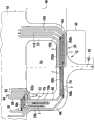
图1示出微机械构件的第一实施方式的横截面。FIG. 1 shows a cross section of a first embodiment of a micromechanical component.
示出的微机械构件的横截面沿弹簧12的纵轴线10延伸,可调元件14通过所述弹簧12与微机械构件的保持装置16连接。弹簧12可以由单晶硅材料结构化形成。用于弹簧12的优选材料是硅。优选地,弹簧12的纵轴线10沿单晶硅材料的110晶体方向延伸。如以下仍要详细阐述的,这种弹簧12简化了惠斯通电桥和/或x-ducer的实现。首先在此情况下,可容易地实施惠斯通电桥或x-ducer的压阻传感器元件的有利定向。特别地,弹簧12可以与保持装置16和/或可调元件14的至少一个子单元一体地构造。The illustrated cross-section of the micromechanical component extends along the
在示出的实施例中,弹簧12的与保持装置16相邻的第一端部区段具有穿通的槽口,所述槽口将弹簧12划分为第一臂,(未示出的)第二臂和连接梁。以下更详细地介绍弹簧12的这种构造的优点。In the illustrated embodiment, a first end section of the
除弹簧12以外,微机械构件还可以包括至少一个另外的弹簧,其连接可调元件14和保持装置16。在一个有利的实施方式中,构造为外部弹簧的弹簧12可以将保持装置16与至少一个构造为内部弹簧的另外的弹簧连接,而所述至少一个内部弹簧设置在弹簧12和可调元件14之间。除构造为外部弹簧的弹簧12以外,所述微机械构件还可以包括另一个外部弹簧。以下描述的根据本发明的技术不要求至少一个另外的弹簧。因此在这里描述的实施方式不限于所述至少一个另外的弹簧或者所述至少一个另外的弹簧的确定构造。In addition to the
可调元件14例如可以包括(未示出的)镜板。但需要指出,微机械构件不限于作为微镜的构造。The
在示出的实施方式中,微机械构件包括设置在可调元件14上的执行元件电极梳18和与保持装置16固定连接的定子电极梳20。电极梳18和20是静电驱动装置的子单元,所述静电驱动装置被设计用于相对于保持装置16调节所述可调元件14。但是,微机械构件不限于这种静电驱动装置。作为电极梳18和20的替代方案或补充方案,微机械构件可以包括至少一个另外的电和/或磁的驱动组件。In the illustrated embodiment, the micromechanical component comprises an
优选地,微机械构件的驱动装置被设计用于相对于保持装置16绕弹簧12的纵向10以及绕与纵向10不平行地定向的旋转轴线调节所述可调元件14。在此情况下,也称作双轴悬置的可调元件14。Preferably, the drive of the micromechanical component is designed for adjusting the
示出的微机械构件包括具有(未绘出的)第一压阻传感器元件的第一传感器装置22和具有(未示出的)第二压阻传感器元件的第二传感器装置24。第一压阻传感器元件和第二压阻传感器元件设置在弹簧12上或者弹簧12中。压阻传感器元件设置在弹簧12上或者弹簧12中例如可理解为这些压阻传感器元件的位于弹簧12与保持装置16的第一连接面26和弹簧12与可调元件14的第二连接面28之间的位置。连接面26和28也可以是虚拟的面,即弹簧12的最小端部区段,和/或弹簧12的固定区域。以下更详细地描述传感器装置22和24的压阻传感器元件的有利的实施例和位置。The shown micromechanical component comprises a
在微机械构件上可以通过涂层30和掺杂32构造用于驱动装置和/或传感器装置22和24中的至少一个的电连接的线路。因为对于本领域技术人员而言用于制造弹簧12、具有电极梳18和20的驱动装置以及由涂层30和掺杂32构成的线路的方法根据图1是显而易见的,所以在这里对此进行介绍。The lines for the electrical connection of the drive and/or at least one of the
图2示出微机械构件的第二实施方式的弹簧。FIG. 2 shows a spring of a second embodiment of the micromechanical component.
如果在示出的弹簧12上没有施加负载,则弹簧12位于其初始位置(实线)中。这例如是用于调节微机械构件的可调元件的驱动装置没有运行时的情况。弹簧12在其初始位置中沿其纵轴线10延伸。If no load is applied to the
通过示出的弹簧12,(未绘出的)可调元件与(仅仅部分示出的)保持装置6可调节地连接。优选地,可以绕纵轴线10和与纵轴线10不平行地定向的旋转轴线调节可调元件。有利地,旋转轴线垂直于纵轴线10。可调元件绕纵轴线10和/或旋转轴线的调节运动导致弹簧12的相应的弯曲运动(虚线)。Via the illustrated
如果例如绕纵轴线10旋转可调元件,则这导致弹簧12绕纵轴线10的扭转。弹簧12绕纵轴线10的扭转以下理解为弹簧12的变形,在所述变形时弹簧12的朝着可调元件的第二端部区段被相对于弹簧12的与保持装置16相邻的第一端部区段绕纵轴线10旋转。在弹簧12绕纵轴线10这样扭转时尤其在弹簧12的第一端部区段中出现机械应力。If, for example, the adjustable element is rotated about the
同样地,绕与纵轴线10不平行地定向的旋转轴线调节可调元件导致弹簧12的变形,所述变形以下称作弹簧12绕旋转轴线的弯曲。在弹簧12绕旋转轴线弯曲时,第二端部区段被相对于第一端部区段绕旋转轴线调节。当弹簧12这样弯曲时,在第一端部区段中也出现机械应力。Likewise, adjusting the adjustable element about an axis of rotation oriented non-parallel to the
如以下更详细地描述的那样,微机械构件包括各具有至少一个压阻传感器元件的两个(未示出的)传感器装置。至少两个压阻传感器元件如此设置在弹簧12上或者弹簧12中,使得在弹簧12绕纵轴线10扭转和/或在弹簧12绕旋转轴线弯曲时出现的机械应力作用到至少一个压阻传感器元件上。传感器装置中的每一个被设计用于在机械应力作用到相应的压阻传感器元件上时向微机械构件的(未示出的)分析处理装置提供相应的传感器信号。由传感器装置提供的传感器信号可以包括电压,电压变化,电阻和/或电阻变化。As described in more detail below, the micromechanical component includes two (not shown) sensor arrangements each having at least one piezoresistive sensor element. At least two piezoresistive sensor elements are arranged on or in the
分析处理装置被设计用于在考虑所提供的传感器信号的情况下确定关于可调元件和/或弹簧12绕纵轴线10的第一调节运动和/或弯曲运动的第一信息和关于可调元件和/或弹簧12绕旋转轴线的第二调节运动和/或弯曲运动的第二信息。第一信息和/或第二信息例如可以包括绕纵轴线10调节可调元件和/或弹簧12的第一调节角度,和/或绕旋转轴线旋转可调元件和/或弹簧12的第二调节角度。作为调节角度的替代方案和/或补充方案,第一信息和/或第二信息也可以包括至少一个另外的描述可调元件相对于保持装置的当前位置和/或当前位置变化的量。以下更详细地介绍压阻传感器元件的特别有利的实施方式和位置和分析处理装置的构造。The evaluation device is designed to determine first information about a first adjusting and/or bending movement of the adjustable element and/or
在这里需要指出,在一个唯一的弹簧12上或者中设置两个传感器装置的至少两个压阻传感器元件足以测定或确定关于可调元件和/或弹簧12绕两个彼此不平行的轴线的调节运动和/或弯曲运动的信息。以下详细介绍两个传感器装置的至少两个压阻传感器元件在弹簧12上或者弹簧12中的所述设置的优点,无需使用另一弹簧来设置至少两个压阻传感器元件。It should be pointed out here that the arrangement of at least two piezoresistive sensor elements of two sensor arrangements on or in a
图3A至3C示出用于表示微机械构件的压阻传感器元件的设置可能性的坐标系。示出的坐标系的横坐标相应于单晶硅的100晶体方向。纵坐标给出单晶硅的010晶体方向。3A to 3C show coordinate systems for representing the arrangement possibilities of the piezoresistive sensor elements of the micromechanical component. The abscissa of the shown coordinate system corresponds to the 100 crystal orientation of single-crystal silicon. The ordinate gives the 010 crystal orientation of the single crystal silicon.
在图3A中示意性给出的压阻传感器元件是构造为x-ducer的传感器装置的p掺杂压力单元(Piezo)34a。构造为p掺杂压力单元34a的传感器元件构造在单晶硅中。因为用于在单晶硅层中制造具有p掺杂压力单元34a的x-ducer的方法对于本领域技术人员而言是已知的,对此不进行介绍。The piezoresistive sensor element shown schematically in FIG. 3A is a p-doped pressure cell (Piezo) 34 a of a sensor device designed as an x-ducer. The sensor element embodied as p-doped
x-ducer被如此构造,使得作用到p掺杂压力单元34a上的机械应力导致电压变化。如果电流j被传导通过p掺杂压力单元34a,则可以通过量取p掺杂压力单元34a上的电压U来测定电压变化。当p掺杂压力单元34a位于单晶硅层的100晶体方向上并且作用到p掺杂压力单元34a上的机械应力平行或垂直于单晶硅层的100晶体方向定向时,存在最大电压变化。The x-ducer is designed in such a way that a mechanical stress acting on the p-doped
因此,为了实现传感器装置的可靠功能,p掺杂压力单元34a沿100晶体方向定向。在p掺杂压力单元34a如此定向时,电流j优选沿100晶体方向被引导通过p掺杂压力单元34a。垂直于电流j地量取p掺杂压力单元34a上的电压U。Therefore, in order to achieve a reliable function of the sensor arrangement, the p-doped
图3B给出了半桥和/或构造为惠斯通电桥的传感器装置的p掺杂电阻34b的优选定向。惠斯通电桥可以包括四个构造为压阻传感器元件的p掺杂电阻34b。FIG. 3B shows a preferred orientation of the p-doped
优选地,惠斯通电桥的p掺杂电阻34b如此嵌入到单晶硅中,使得p掺杂电阻34b沿单晶硅的110晶体方向定向并且电流j沿110晶体方向被引导通过p掺杂电阻34b。作为惠斯通电桥的传感器信号,量取四个p掺杂电阻34b上的电阻R/电阻变化。有利地,垂直于至少一个p掺杂电阻34b的定向地量取电阻R/电阻变化。Preferably, the p-doped
借助图3C示出的传感器装置包括电阻,半桥和/或连接为惠斯通电桥的四个n掺杂电阻34c。当四个n掺杂电阻34c在单晶硅的100晶体方向上定向并且机械应力与100晶体方向平行或垂直地作用到四个n掺杂电阻34c上时,在这种惠斯通电桥中存在最大电阻变化。The sensor arrangement shown with reference to FIG. 3C comprises a resistor, a half bridge and/or four n-doped
因此,惠斯通电桥如此设置在单晶硅上或单晶硅中,使得n掺杂电阻34c中的至少一个沿100晶体方向定向并且电流j沿100晶体方向被引导通过n掺杂电阻34c。在此情况下,也可以测量n掺杂电阻34c上的电阻R/电阻变化。通过n掺杂电阻34c的这种有利定向,施加到n掺杂电阻34c上的机械应力导致最大电阻变化。优选地,在n掺杂电阻34c上与电流j垂直地测量电阻R/电阻变化。The Wheatstone bridge is thus arranged on or in the single-crystal silicon such that at least one of the n-doped
可成本有利地并且相对容易地制造具有至少一个p掺杂压力单元34a的传感器装置22或24和/或具有四个电阻34b或34c的惠斯通电桥。以下更详细地介绍在微机械构件的弹簧12上设置至少一个p掺杂压力单元34a、至少一个p掺杂电阻34b和/或至少一个n掺杂电阻34c的其他有利示例。A
图4示出微机械构件的第三实施方式的弹簧。FIG. 4 shows a spring of a third embodiment of the micromechanical component.
示出的弹簧12如此由单晶硅结构化形成,使得(在初始位置中)弹簧12的纵向10沿单晶硅的110晶体方向延伸。(未绘出的)可调元件通过所述弹簧12与保持装置16连接。The illustrated
弹簧12的平均宽度可以在50μm以下。例如,弹簧12的平均宽度在10和30μm之间。弹簧12的与保持装置16相邻设置的第一端部区段40的最大宽度大于朝着可调元件定向的第二端部区段42的最大宽度。同样地,第一端部区段40的最大宽度大于弹簧12的中间区段43的最大宽度,所述中间区段从第一端部区段40延伸到第二端部区段42。这可以称作第一端部区段40与弹簧12的第二端部区段42和/或中间区段43相比的加宽。The average width of the
优选地,第一端部区段40的宽度沿从中间区段43到保持装置16的方向持续增大。这也可以称作弹簧12与保持装置16的实心V形弹簧连接。Preferably, the width of the
在第一端部区段40上或者在第一端部区段40中设置有构造为x-ducer的第一传感器装置22的第一p掺杂压力单元34a和构造为x-ducer的第二传感器装置24的第二p掺杂压力单元34a。充当传感器装置22和24的x-ducer中的每一个被如此设计,使得作用到从属的p掺杂压力单元34a上的机械应力导致垂直于电流j定向的电压U的变化,电流j被引导通过所述p掺杂压力单元34a。优选地,垂直于电流j地测量电压U的变化。Arranged on or in the
在沿单晶硅的110晶体方向的弹簧12的纵轴线10中,有利地引导电流j如此通过p掺杂压力单元34a,使得电流j以相对于纵轴线10成45°的角度定向。因此,通过p掺杂压力单元34a的电流j沿100晶体方向定向。In the
可在第一传感器装置22的p掺杂压力单元34a中实现电流j的这种有利定向,其方式是,第一电流供给线路44和第二电流供给线路46如此接触第一传感器装置22的p掺杂压力单元34a,使得两个电流供给线路44和46之间的最小距离沿100晶体方向延伸。附加地,第二电流供给线路46和第三电流供给线路48可以如此接触第二传感器装置24的p掺杂压力单元34a,使得两个电流供给线路46和48之间的最短距离沿100晶体方向定向。通过电流供给线路44至48与电流源的适当连接,可以确保足够的电流j流过两个传感器装置22和24的p掺杂压力单元34a。例如电流供给线路44和48可以连接到电流源的正极上,而电流供给线路46可以连接到电流源的负极上。但对于本领域技术人员而言,也可以通过图4得出电流供给线路44至48的其他可能极性。Such an advantageous orientation of the current j in the p-doped
通过由共同的第二电流供给线路46接触两个传感器装置22和24的两个p掺杂压力单元34a,可实现用于两个传感器装置22和24的两个p掺杂压力单元34a的电流供给的电流供给线路44至48的相对较少数量。因此,电流供给线路44至48仅仅在很小的程度上影响具有两个传感器装置22和24的两个p掺杂压力单元34a的弹簧12的弹簧坚固性。这是在这里描述的实施方式相对于现有技术的重要优点,在现有技术中两个p掺杂压力单元34a在两个弹簧上的设置需要更大数量的用于两个p掺杂压力单元34a的电流供给的电流供给线路。单晶硅具有高机械稳定性,但作为半导体也具有相对较高的电阻。为了使所述电阻保持得较低,附加地有利地通过弹簧12引导数量尽可能少的电流供给线路44至48。The current flow for the two p-doped
两个电压量取线路50和52与第一传感器装置22的p掺杂压力单元34a连接。优选地,如此选择两个电压量取线路50和52的位置,使得两个电压量取线路50和52之间的最小距离沿单晶硅的010晶体方向定向。相应地,两个电压量取线路54和56可以如此接触第二传感器装置24的p掺杂压力单元34a,使得两个电压量取线路54和56之间的最小距离同样沿010晶体方向延伸。因此,构造用于量取电压U的电压量取线路50至56被如此构造,使得沿010晶体方向进行电压U的量取。这确保了两个传感器装置22和24的两个p掺杂压力单元34a最佳地用于通过以下描述的方式测定作用到两个传感器装置22和24的两个p掺杂压力单元34a上的机械应力或者确定关于可调元件和/或弹簧12的调节运动和/或弯曲运动的信息。The two voltage taps 50 and 52 are connected to the p-doped
在第一端部区段40的V形构造的情况下,可以确保用于两个传感器装置22和24的两个p掺杂压力单元34a和线路44至56的足够的安装面。因为线路44至56不沿弹簧12超出第一端部区段40,所述它们几乎不损害弹簧12的弹簧坚固性。With the V-shaped configuration of the
两个传感器装置22和24的两个p掺杂压力单元34a可以具有与弹簧12和保持装置16之间的(虚拟)连接面26的相同距离。两个传感器装置22和24的两个p掺杂压力单元34a同样可以具有与优选位于纵轴线10上的中点60的相同距离。在两个传感器装置22和24的两个p掺杂压力单元34a这样设置时,在绕与纵轴线10不平行地定向的旋转轴线弯曲弹簧12时或者在绕所述旋转轴线调节可调元件时,施加到两个p掺杂压力单元34a上的机械应力几乎是相同的。与此相对地,在两个p掺杂压力单元34a这样设置时,弹簧12绕纵轴线10的扭转或者可调元件绕纵轴线10的调节导致不同的机械应力作用到两个传感器装置22和24的两个p掺杂压力单元34a上。在两种情况下,机械应力都包括110晶体方向上的干扰应力。The two p-doped
优选地,在两个传感器装置22和24的两个p掺杂压力单元34a这样设置时,(未示出的)分析处理装置被设计用于,在考虑作为第一传感器信号提供的第一传感器装置22的第一电压信号和作为第二传感器信号提供的第二传感器装置22的第二电压信号的差的情况下,确定关于可调元件和/或弹簧12绕纵轴线10的第一调节运动和/或弯曲运动的第一信息。附加地,分析处理装置还可以被设计用于,在考虑第一电压信号和第二电压信号的平均值的情况下,确定关于可调元件和/或弹簧12绕与纵轴线10不平行的旋转轴线的第二调节运动和/或弯曲运动的第二信息。通过所述方式可以确保用于确定可靠的第一信息和可靠的第二信息的相对较少的耗费。Preferably, when the two p-doped
在一个替代实施方式中,弹簧12也可以被如此构造,使得(在初始位置中)弹簧12的纵向10沿弹簧材料、优选硅的100晶体方向定向。优选地,在弹簧12这样构造时,对于两个传感器装置22和24分别使用一个x-ducer,其与100晶体方向或弹簧12的纵向10平行地定向。如果两个传感器装置22和24具有n掺杂电阻,则它们优选以在图4中示出的方式定向。在使用用于两个传感器装置22和24的p掺杂电阻时,其定向优选旋转45°。在所有在这里列举的实施方式中,两个传感器装置22和24的压阻元件设置在沿100晶体方向构造的弹簧12的以下区域中:在所述区域中在弹簧12弯曲和/或扭转时出现最大的机械应力。In an alternative embodiment, the
图5示出微机械构件的第四实施方式的弹簧。FIG. 5 shows a spring of a fourth embodiment of the micromechanical component.
在示出的弹簧12中,作为图4的实施方式的补充,在第一端部区段40内构造有穿通的槽口62,所述槽口将第一端部区段40划分为第一臂64和第二臂66。优选地,两个臂64和66构成V形结构。In the
优选地,第一传感器装置22的p掺杂压力单元34a设置在第一臂64上或第一臂64中而第二传感器装置24的p掺杂压力单元34a设置在第二臂66上或第二臂66中。在绕纵轴线10和/或绕与纵轴线10不平行的其他旋转轴线调节可调元件时,在第一端部区段40内构造穿通的槽口62在此情况下导致作用到两个传感器装置22和24的两个p掺杂压力单元34a上的机械应力的增强。因此,两个传感器装置22和24的两个p掺杂压力单元34a有针对性地设置在弹簧12扭转和/或弹簧12绕旋转轴线弯曲时具有相对较高的机械应力的弹簧区段上。通过所述方式可以更精确地确定第一信息和第二信息。Preferably, the p-doping
图6示出微机械构件的第五实施方式的弹簧。FIG. 6 shows a spring of a fifth embodiment of the micromechanical component.
示出的弹簧12如此由单晶硅结构化形成,使得纵轴线10沿单晶硅的110晶体方向定向。(未绘出的)可调元件通过弹簧12与保持装置16连接。优选地,弹簧12与保持装置16的至少一个子单元和/或可调元件的至少一个子单元一体地构造。The illustrated
弹簧12的与保持装置16相邻设置的第一端部区段40相对于朝着可调元件定向的第二端部区段42和/或中间区段43加宽。在图6的示出的示例中,第二端部区段42和中间区段43具有10至20μm的平均宽度。与此相对地,第一端部区段40的两个外侧面彼此的距离在80至150μm之间。A
在第一端部区段40中构造有(穿通的)槽口62,所述槽口将第一端部区段40划分为第一臂70、第二臂72和连接梁74。优选地,连接梁74如此连接第一臂70和第二臂72,从而构成U形结构。特别地,第一臂70可以与第二臂72平行地定向。A (through)
在示出的弹簧12中,第一传感器装置22至少部分在构造在第一臂70上。第一传感器装置22是具有四个p掺杂电阻76b至82b的惠斯通电桥。第一p掺杂电阻76b和第二p掺杂电阻78b设置在第一臂70上。第三p掺杂电阻80b和第四p掺杂电阻82b优选如此设置在保持装置16上,使得它们位于第一臂70的固定区域内或者附近。In the
第一电流供给线路84接触第一传感器装置22的第一p掺杂电阻76b。此外,第一p掺杂电阻76b通过测量线路86与第一传感器装置22的第三p掺杂电阻80b连接。第二电流供给线路88也与第一传感器装置22的第三p掺杂电阻80b连接。第一电流供给线路84和第二电流供给线路88如此接触第一传感器装置22的第一p掺杂电阻76b和第三p掺杂电阻80b,使得电流j沿110晶体方向、即与弹簧12的纵轴线10平行或垂直地流过第一传感器装置22的第一p掺杂电阻76b和第三p掺杂电阻80b。The first
第一传感器装置22的第二p掺杂电阻78b与第三电流供给线路90和第二测量线路92连接。第二测量线路92将第一传感器装置22的第二p掺杂电阻78b与第四p掺杂电阻82b连接,第四电流供给线路94也与第四p掺杂电阻82b连接。第三电流供给线路90和第四电流供给线路94如此接触第一传感器装置22的第二p掺杂电阻78b或第四p掺杂电阻82b,使得电流j与弹簧12的纵轴线10平行或垂直地流过第一传感器装置22的第二p掺杂电阻78b和第四p掺杂电阻82b。因此,确保了沿单晶硅的110晶体方向引导电流j。The second p-doped
例如,第一电流供给线路84与电流源的正极连接,而第二电流供给线路88与电流源的负极连接。在此情况下,有利地将第三电流供给线路90连接到电流源的负极上并且将第四电流供给线路94连接到电流源的正极上。For example, the first
第一测量线路86和第二测量线路92被设计用于量取第一传感器22的四个p掺杂电阻76b至82b上的电阻R或者电阻变化,作为第一传感器信号。因为具有四个p掺杂电阻76b至82b的惠斯通电桥的功能对于本领域技术人员而言是已知的,所以在这里不更详细地对此进行介绍。The
在弹簧12上还设置有第二传感器装置24,所述第二传感器装置24被构造为具有四个p掺杂电阻96b至102b的惠斯通电桥。优选地,第二传感器装置24的四个p掺杂电阻96b至102b至少部分地位于连接梁74上。特别地,第一p掺杂电阻96b和第二p掺杂电阻98b可以位于纵轴线10的第一侧上。在此情况下,第三p掺杂电阻100b和第四p掺杂电阻102b优选设置在纵轴线10的第二侧上。Also arranged on the
在示出的示例中,第二传感器装置24的第一p掺杂电阻96b与第一电流供给线路84和第三测量线路104接触。第三测量线路104将第二传感器装置24的第一p掺杂电阻96b和第三p掺杂电阻100b连接。第五电流供给线路106与第三p掺杂电阻100b连接。优选地,第一电流供给线路84和第五电流供给线路106如此接触第一p掺杂电阻96b或第三p掺杂电阻100b,使得电流j与纵轴线10垂直地流过第二传感器装置24的p掺杂电阻96b和100b。在此情况下,流过p掺杂电阻96b和100b的电流j沿弹簧12的单晶硅的110晶体方向定向。如果第一电流供给线路84与电流源的正极连接,则第五电流供给线路106与电流源的负极连接。In the example shown, the first p-doped
此外,第三电流供给线路90接触第二传感器装置24的第二p掺杂电阻98b,所述第二p掺杂电阻98b附加地与第四测量线路108连接。第四测量线路108将第二传感器装置24的第二p掺杂电阻98b和第四p掺杂电阻102b连接。此外,第六电流供给线路110从第二传感器装置24的第四p掺杂电阻102b延伸至电流源。如果第三电流供给线路90接触负极,则第六电流供给线路110与电流源的正极连接。Furthermore, the third
第三电流供给线路90和第六电流供给线路110也可以如此接触第二传感器装置24的为其分配的p掺杂电阻98b和102b,使得电流j沿110晶体方向流过p掺杂电阻98b和102b。通过所述方式可以确保构造为惠斯通电桥的第二传感器装置24的有利且可靠的运行。也可以通过第三测量线路104和第四测量线路108量取p掺杂电阻96b至102b上的电阻R/电阻变化作为第二传感器信号。The third
本领域技术人员借助图6可知,两个传感器装置22和24至少部分地设置在相同的弹簧12上具有以下优点:需要相对较少数量的用于向p掺杂电阻76b至82b和96b至102b供电的电流供给线路84、88、90、94、106和110。通过所述方式可以确保:弹簧12的弯曲坚固性和可调元件的良好可调节性几乎不受电流供给线路84、88、90、94、106和110的影响。同样可以确保:弹簧12、尤其是第二端部区段42和/或中间区段43的弯曲和/或可调元件的调节几乎不或者仅仅略微地影响可能也压阻反应的电流供给线路84、88、90、94、106和110。附加地,通过所述方式可减少用于构成电流供给线路84、88、90、94、106和110的工作耗费。A person skilled in the art can see from FIG. 6 that the arrangement of the two
以下描述如何在考虑第一传感器装置22的第一传感器信号和第二传感器装置24的第二传感器信号的情况下以少量的耗费并且可靠地确定关于弹簧12和/或可调元件的调节运动和/或弯曲运动的信息:The following describes how to reliably determine the adjustment movements and / or information about bending motion:
由于第一端部区段40中的穿通槽口62,弹簧12的弯曲导致两个臂70和72与连接梁74上的机械应力增强。在弹簧12绕纵轴线10扭转时,在连接梁74中出现相对较高的机械应力,而在两个臂70和72中引起的机械应力保持相对较低。因此,在弹簧12绕纵轴线10扭转时出现的机械应力主要影响第二传感器装置24的第二传感器信号。因此,微机械构件的(未绘出的)分析处理装置有利地被设计用于根据第二传感器信号确定关于弹簧12和/或可调元件绕纵轴线10的第一调节运动和/或弯曲运动(扭转)的第一信息。Due to the through-
在绕与纵轴线10不平行的旋转轴线调节可调元件以及与此相关联地绕所述旋转轴线弯曲弹簧12时,相对于连接梁74中的机械应力增强臂70和72中的机械应力。特别地,当所述旋转轴线与纵轴线10垂直地定向时,弹簧12绕所述旋转轴线的弯曲导致臂70和72中相对较高的机械应力,而连接梁74中所触发的机械应力保持相对较低。When the adjustable element is adjusted about an axis of rotation that is not parallel to the
因此,第二传感器装置24如此设置在弹簧12上,使得可通过第二传感器信号良好地确定弹簧12绕纵轴线10的扭转,通过第一传感器装置22至少部分地设置在第一臂70上或第一臂70中可以确保:虽然弹簧12绕纵轴线10的扭转几乎不引起作用到四个p掺杂电阻76b至82b上的机械应力,但弹簧12绕旋转轴线的弯曲导致作用到第一传感器装置22的四个p掺杂电阻76b至82b上的相对较高的机械应力。因此,分析处理装置优选被设计用于根据第一传感器信号确定关于弹簧12和/或可调元件绕旋转轴线的调节运动和/或弯曲运动的第二信息。Therefore, the
在弹簧12的替代构造中,纵轴线10可以沿100晶体方向定向。优选地,传感器装置22和24在此情况下包括具有在图6示出的设置和定向的n掺杂电阻。只要四个p掺杂电阻76b至82b和96b至102b分别用于传感器22和24,则p掺杂电阻76b至82b和96b至102b的定向相应匹配。In an alternative configuration of the
图7示出微机械构件的第六实施方式的弹簧。FIG. 7 shows a spring of a sixth embodiment of the micromechanical component.
示出的弹簧12如此由单晶硅结构化形成,使得弹簧12的纵轴线10沿110晶体方向延伸。弹簧12的与保持装置16相邻构造的第一端部区段40的最小宽度大于弹簧12朝着可调元件定向的第二端部区段42和/或中间区段43的最小宽度。例如,第二端部区段42和/或中间区段43的平均宽度在10至20μm之间。与此相对地,第一端部区段40的宽度随着与保持装置16的距离的增大而不断减小,其中,所述宽度尤其在50至150μm的范围内。The illustrated
在第一端部区段40中构造有穿通的槽口62,所述槽口62将第一端部区段40划分为第一臂64和第二臂66。优选地,两个臂64和66构成V形结构。A through
在示出的弹簧12上至少部分地构造有第一传感器装置22,第二传感器装置24,电流供给线路84、88、90、94、106和110以及测量线路86、92、104和108。但是,与以上实施方式不同,传感器装置22和24构造为具有各四个n掺杂电阻76c至82c或96c至102c的惠斯通电桥。
电流供给线路84、88、90、94、106和110如此接触为其分配的电阻76c至82c和96c至102c,使得电流j以相对于弹簧12的沿110晶体方向定向的纵轴线10成45°的角度流过电阻76c至82c和96c至102c中的每一个。因此,流过电阻76c至82c和96c至102c的电流j的定向对应于图3C的有利的定向。相应地,测量线路86、92、104和108也被如此构造,使得以相对于纵轴线10或者相对于110晶体方向成45°的角度进行电阻R/电阻变化的测量。电流供给线路84、88、90、94、106和110和测量线路86、92、104和108满足以上已经描述的功能。因此,在这里不进一步描述电流供给线路84、88、90、94、106和110和测量线路86、92、104和108的功能。The
通过第一端部区段40的V形结构可以确保:足够的安装面可供用于根据n掺杂电阻76c至82c和96c至102c沿100晶体方向的优选定向在第一臂64上施加n掺杂电阻76c至82c以及在第二臂66上施加n掺杂电阻96c至102c。此外,还可以确保用于形成电流供给线路84、88、90、94、106和110和测量线路86、92、104和108的足够大的安装面。The V-shaped structure of the
在弹簧12绕纵轴线10扭转时,作用到n掺杂电阻76c至82c上的机械应力明显不同于施加到n掺杂电阻96c至102c上的机械应力。出于这个原因,第一传感器信号和第二传感器信号之间的差特别适于确定关于弹簧12和/或可调元件绕纵轴线10的第一调节运动和/或弯曲运动的第一信息。与此相对地,弹簧12绕旋转轴线的弯曲导致作用到n掺杂电阻76c至82c和96c至102c上的几乎相同的机械应力。When
因此,分析处理装置优选地被设计用于在考虑第一传感器信号和第二传感器信号的差的情况下确定第一信息以及在考虑第一传感器信号和第二传感器信号的平均值的情况下确定第二信息。The evaluation device is therefore preferably designed to determine the first information taking into account the difference between the first sensor signal and the second sensor signal and to determine the mean value of the first sensor signal and the second sensor signal second information.
在一个替代的实施方式中,具有子单元70至74的弹簧12的纵轴线10可以沿构造弹簧12的硅材料层的100晶体方向定向。在此情况下,传感器装置22和24至少之一的p掺杂电阻根据图7相对于纵轴线10定向。如果传感器装置22和24至少之一包括n掺杂电阻76c至82c和96c至102c,则它们相对于在图7中示出的定向旋转45°地设置。在两种情况下,传感器装置22和24可以设置在最大机械应力的范围内。In an alternative embodiment, the
借助于以上所述的实施方式之一确定的关于弹簧12和/或可调元件的调节运动和/或弯曲运动的信息可以用于控制和/或检验微机械构件的驱动。对于微机械构件的驱动的调节控制,可调元件的当前位置的精确探测是有利的。作为替代方案或补充方案,也可以使用由分析处理装置确定的信息来检验可调元件是否已被可靠置于优选位置中。因此,通过分析由分析处理装置提供的信息可在将可调元件调节到优选位置中时实现更好的精确度。The information determined with the aid of one of the embodiments described above regarding the adjusting and/or bending movements of the
在构造为传感器的微机械构件中,由分析处理装置提供的信息也可以用于测定/确定关于作用到可调元件上的外力的传感器信息。因此,在这里描述的微机械构件既可用作执行元件也可用作传感器。In the case of micromechanical components designed as sensors, the information provided by the evaluation device can also be used to determine/determine sensor information about external forces acting on the adjustable element. The micromechanical components described here can thus be used both as actuators and as sensors.
根据以上所述的两种实施方式,对于本领域技术人员而言,传感器装置22和/或24的以下构造也是显而易见的:取代惠斯通电桥而使用单个电阻和/或半桥。同样根据附图,具有至少一个设置在弹簧的固定区域上或固定区域中的压阻传感器元件的实施方式对于本领域技术人员而言显而易见的。因此,不进一步介绍传感器装置22和/或24的这种构造和设置可能性。The configuration of the
本领域技术人员同样可知,传感器装置22和/或24也可以包括不同的压阻传感器元件。为此不再描述以上实施方式的这种组合。A person skilled in the art is also aware that
Claims (11)
Applications Claiming Priority (3)
| Application Number | Priority Date | Filing Date | Title |
|---|---|---|---|
| DE102009026506ADE102009026506A1 (en) | 2009-05-27 | 2009-05-27 | Micromechanical component and production method for a micromechanical component |
| DE102009026506.6 | 2009-05-27 | ||
| PCT/EP2010/056806WO2010136356A2 (en) | 2009-05-27 | 2010-05-18 | Micromechanical component, and method for the production thereof |
Publications (2)
| Publication Number | Publication Date |
|---|---|
| CN102448872Atrue CN102448872A (en) | 2012-05-09 |
| CN102448872B CN102448872B (en) | 2015-06-03 |
Family
ID=43028602
Family Applications (1)
| Application Number | Title | Priority Date | Filing Date |
|---|---|---|---|
| CN201080023335.5AActiveCN102448872B (en) | 2009-05-27 | 2010-05-18 | Micromechanical components and manufacturing methods for micromechanical components |
Country Status (7)
| Country | Link |
|---|---|
| US (1) | US8813573B2 (en) |
| EP (1) | EP2435354B1 (en) |
| JP (1) | JP5474183B2 (en) |
| KR (1) | KR101765343B1 (en) |
| CN (1) | CN102448872B (en) |
| DE (1) | DE102009026506A1 (en) |
| WO (1) | WO2010136356A2 (en) |
Cited By (2)
| Publication number | Priority date | Publication date | Assignee | Title |
|---|---|---|---|---|
| TWI582667B (en)* | 2015-06-10 | 2017-05-11 | 宸鴻科技(廈門)有限公司 | Pressure sensing pattern layer and pressure sensing input device including the same |
| CN113474281A (en)* | 2019-01-25 | 2021-10-01 | 罗伯特·博世有限公司 | MEMS sensor and method for operating a MEMS sensor |
Families Citing this family (4)
| Publication number | Priority date | Publication date | Assignee | Title |
|---|---|---|---|---|
| DE102012219660B4 (en)* | 2012-10-26 | 2023-10-12 | Robert Bosch Gmbh | Mechanical component |
| DE102013217094B4 (en)* | 2013-08-28 | 2021-11-04 | Robert Bosch Gmbh | Micromechanical component and corresponding test method for a micromechanical component |
| DE102021201243A1 (en) | 2021-02-10 | 2022-08-11 | Robert Bosch Gesellschaft mit beschränkter Haftung | mechanical component |
| DE102023203335A1 (en)* | 2023-04-13 | 2024-10-17 | Robert Bosch Gesellschaft mit beschränkter Haftung | Micromechanical component and scanning device |
Citations (4)
| Publication number | Priority date | Publication date | Assignee | Title |
|---|---|---|---|---|
| JPH0996552A (en)* | 1995-09-29 | 1997-04-08 | Omron Corp | Sensor device |
| JP2004245890A (en)* | 2003-02-10 | 2004-09-02 | Denso Corp | Optical scanning device |
| JP2007307662A (en)* | 2006-05-18 | 2007-11-29 | Seiko Epson Corp | Actuator |
| US20080144154A1 (en)* | 2005-07-21 | 2008-06-19 | Brother Kogyo Kabushiki Kaisha | Optical scan device, image display device, method of modifying resonance frequency of optical scanner, and method of correcting position of reflection mirror |
Family Cites Families (10)
| Publication number | Priority date | Publication date | Assignee | Title |
|---|---|---|---|---|
| JP2981600B2 (en) | 1996-01-17 | 1999-11-22 | オムロン株式会社 | Optical scanner and optical sensor device using the same |
| JP2002250890A (en) | 2001-02-22 | 2002-09-06 | Canon Inc | Microstructure, micro-optical deflector, optical scanning display device and method of manufacturing the same |
| AU2003223125A1 (en) | 2002-04-17 | 2003-11-03 | M2N Inc. | Micro piezoelectric actuator and method for fabricating same |
| JP2005279863A (en) | 2004-03-30 | 2005-10-13 | Seiko Epson Corp | Actuator manufacturing method and actuator |
| JP2006195290A (en) | 2005-01-14 | 2006-07-27 | Ricoh Co Ltd | Image reading apparatus and image forming apparatus |
| US7250705B2 (en)* | 2005-09-16 | 2007-07-31 | Texas Instruments Incorporated | Resonant oscillating device actuator structure |
| KR100868758B1 (en) | 2007-01-15 | 2008-11-13 | 삼성전기주식회사 | Rotating MEMS devices with piezoresistive sensors |
| EP2347506B1 (en)* | 2008-10-14 | 2013-01-09 | Nxp B.V. | Frame-shaped mems piezoresistive resonator |
| US8187903B2 (en)* | 2009-01-13 | 2012-05-29 | Robert Bosch Gmbh | Method of epitaxially growing piezoresistors |
| US8264797B2 (en)* | 2009-12-21 | 2012-09-11 | Western Digital (Fremont), Llc | Head gimbal assembly having a radial rotary piezoelectric microactuator between a read head and a flexure tongue |
- 2009
- 2009-05-27DEDE102009026506Apatent/DE102009026506A1/ennot_activeWithdrawn
- 2010
- 2010-05-18JPJP2012512304Apatent/JP5474183B2/enactiveActive
- 2010-05-18USUS13/321,625patent/US8813573B2/enactiveActive
- 2010-05-18EPEP10721776.2Apatent/EP2435354B1/enactiveActive
- 2010-05-18CNCN201080023335.5Apatent/CN102448872B/enactiveActive
- 2010-05-18WOPCT/EP2010/056806patent/WO2010136356A2/enactiveApplication Filing
- 2010-05-18KRKR1020117028181Apatent/KR101765343B1/enactiveActive
Patent Citations (4)
| Publication number | Priority date | Publication date | Assignee | Title |
|---|---|---|---|---|
| JPH0996552A (en)* | 1995-09-29 | 1997-04-08 | Omron Corp | Sensor device |
| JP2004245890A (en)* | 2003-02-10 | 2004-09-02 | Denso Corp | Optical scanning device |
| US20080144154A1 (en)* | 2005-07-21 | 2008-06-19 | Brother Kogyo Kabushiki Kaisha | Optical scan device, image display device, method of modifying resonance frequency of optical scanner, and method of correcting position of reflection mirror |
| JP2007307662A (en)* | 2006-05-18 | 2007-11-29 | Seiko Epson Corp | Actuator |
Non-Patent Citations (1)
| Title |
|---|
| CHI ZHANG, ET AL.: "A Two-Dimensional Micro Scanner Integrated with a Piezoelectric Actuator and Piezoresistors", 《SENSORS》, vol. 9, no. 1, 23 January 2009 (2009-01-23), pages 631 - 644, XP002620220, DOI: doi:10.3390/s90100631* |
Cited By (3)
| Publication number | Priority date | Publication date | Assignee | Title |
|---|---|---|---|---|
| TWI582667B (en)* | 2015-06-10 | 2017-05-11 | 宸鴻科技(廈門)有限公司 | Pressure sensing pattern layer and pressure sensing input device including the same |
| CN113474281A (en)* | 2019-01-25 | 2021-10-01 | 罗伯特·博世有限公司 | MEMS sensor and method for operating a MEMS sensor |
| US12145840B2 (en) | 2019-01-25 | 2024-11-19 | Robert Bosch Gmbh | MEMS sensor as well as method for operating a mems sensor |
Also Published As
| Publication number | Publication date |
|---|---|
| US20120125117A1 (en) | 2012-05-24 |
| EP2435354A2 (en) | 2012-04-04 |
| JP5474183B2 (en) | 2014-04-16 |
| KR20120029403A (en) | 2012-03-26 |
| EP2435354B1 (en) | 2013-07-24 |
| DE102009026506A1 (en) | 2010-12-02 |
| JP2012528014A (en) | 2012-11-12 |
| CN102448872B (en) | 2015-06-03 |
| KR101765343B1 (en) | 2017-08-07 |
| WO2010136356A2 (en) | 2010-12-02 |
| WO2010136356A3 (en) | 2011-04-14 |
| US8813573B2 (en) | 2014-08-26 |
Similar Documents
| Publication | Publication Date | Title |
|---|---|---|
| CN102448872B (en) | Micromechanical components and manufacturing methods for micromechanical components | |
| JP4773421B2 (en) | Rotating MEMS device | |
| US7508189B2 (en) | Micro-electromechanical system (MEMS) based current and magnetic field sensor having improved sensitivities | |
| US20040079154A1 (en) | Acceleration sensor | |
| US20040025591A1 (en) | Accleration sensor | |
| US10913652B2 (en) | Micromechanical z-inertial sensor | |
| US20100011860A1 (en) | Micromechanical sensor element, method for manufacturing a micromechanical sensor element and method for operating a micromechanical sensor element | |
| CN104418290B (en) | Micro-mechanical component and the method for manufacturing micro-mechanical component | |
| CN111226155B (en) | Micromechanical micromirror assembly and corresponding operating method | |
| US10408695B2 (en) | Piezoresistive position sensor systems | |
| CN102692705A (en) | MOEMS (Micro Optoelectro Mechanical System)-process-based micro scanning raster based on of integrating angle sensor | |
| US10246318B2 (en) | Micromechanical component and production method for a micromechanical component | |
| JP4749790B2 (en) | Micromirror device and manufacturing method thereof, angle measurement method of micromirror device, and micromirror device application apparatus | |
| US20110226059A1 (en) | Sensor and method for manufacturing a sensor | |
| KR20130038751A (en) | Scanning micromirror including temperature compensating function of sensor and compensating method thereof | |
| EP4314930B1 (en) | Sensor based control of an optical device with a variable optical power or a variable beam deflection | |
| JP6521442B2 (en) | Pressure sensor | |
| CN109387659B (en) | Rotation speed sensor, method for producing a rotation speed sensor | |
| US8462415B2 (en) | Connecting structure for micromechanical oscillating devices | |
| JP2007298408A (en) | Electrostatic capacity sensor | |
| Luo et al. | Design of a MOEMS-based electromagnetic driven high efficacious phase grating with angle sensor |
Legal Events
| Date | Code | Title | Description |
|---|---|---|---|
| C06 | Publication | ||
| PB01 | Publication | ||
| C10 | Entry into substantive examination | ||
| SE01 | Entry into force of request for substantive examination | ||
| C14 | Grant of patent or utility model | ||
| GR01 | Patent grant |