CN102447020A - Method for manufacturing high-brightness vertical light-emitting diodes - Google Patents
Method for manufacturing high-brightness vertical light-emitting diodesDownload PDFInfo
- Publication number
- CN102447020A CN102447020ACN2010105093269ACN201010509326ACN102447020ACN 102447020 ACN102447020 ACN 102447020ACN 2010105093269 ACN2010105093269 ACN 2010105093269ACN 201010509326 ACN201010509326 ACN 201010509326ACN 102447020 ACN102447020 ACN 102447020A
- Authority
- CN
- China
- Prior art keywords
- acid
- substrate
- solution
- hydroxide
- material layers
- Prior art date
- Legal status (The legal status is an assumption and is not a legal conclusion. Google has not performed a legal analysis and makes no representation as to the accuracy of the status listed.)
- Pending
Links
- 238000000034methodMethods0.000titleclaimsabstractdescription32
- 238000004519manufacturing processMethods0.000titleclaimsabstractdescription19
- 239000000758substrateSubstances0.000claimsabstractdescription69
- 239000000463materialSubstances0.000claimsabstractdescription18
- WGTYBPLFGIVFAS-UHFFFAOYSA-Mtetramethylammonium hydroxideChemical compound[OH-].C[N+](C)(C)CWGTYBPLFGIVFAS-UHFFFAOYSA-M0.000claimsdescription38
- HEMHJVSKTPXQMS-UHFFFAOYSA-MSodium hydroxideChemical compound[OH-].[Na+]HEMHJVSKTPXQMS-UHFFFAOYSA-M0.000claimsdescription30
- 239000002253acidSubstances0.000claimsdescription23
- VEXZGXHMUGYJMC-UHFFFAOYSA-NHydrochloric acidChemical compoundClVEXZGXHMUGYJMC-UHFFFAOYSA-N0.000claimsdescription20
- KWYUFKZDYYNOTN-UHFFFAOYSA-MPotassium hydroxideChemical compound[OH-].[K+]KWYUFKZDYYNOTN-UHFFFAOYSA-M0.000claimsdescription19
- QTBSBXVTEAMEQO-UHFFFAOYSA-NAcetic acidChemical compoundCC(O)=OQTBSBXVTEAMEQO-UHFFFAOYSA-N0.000claimsdescription15
- KRHYYFGTRYWZRS-UHFFFAOYSA-NFluoraneChemical compoundFKRHYYFGTRYWZRS-UHFFFAOYSA-N0.000claimsdescription15
- MUBZPKHOEPUJKR-UHFFFAOYSA-NOxalic acidChemical compoundOC(=O)C(O)=OMUBZPKHOEPUJKR-UHFFFAOYSA-N0.000claimsdescription15
- BDAGIHXWWSANSR-UHFFFAOYSA-Nmethanoic acidNatural productsOC=OBDAGIHXWWSANSR-UHFFFAOYSA-N0.000claimsdescription15
- 239000000203mixtureSubstances0.000claimsdescription14
- NBIIXXVUZAFLBC-UHFFFAOYSA-NPhosphoric acidChemical compoundOP(O)(O)=ONBIIXXVUZAFLBC-UHFFFAOYSA-N0.000claimsdescription10
- CDBYLPFSWZWCQE-UHFFFAOYSA-LSodium CarbonateChemical compound[Na+].[Na+].[O-]C([O-])=OCDBYLPFSWZWCQE-UHFFFAOYSA-L0.000claimsdescription10
- QAOWNCQODCNURD-UHFFFAOYSA-NSulfuric acidChemical compoundOS(O)(=O)=OQAOWNCQODCNURD-UHFFFAOYSA-N0.000claimsdescription10
- 239000003513alkaliSubstances0.000claimsdescription10
- 235000019253formic acidNutrition0.000claimsdescription10
- 239000000126substanceSubstances0.000claimsdescription10
- UIIMBOGNXHQVGW-UHFFFAOYSA-MSodium bicarbonateChemical compound[Na+].OC([O-])=OUIIMBOGNXHQVGW-UHFFFAOYSA-M0.000claimsdescription8
- -1alkyl sulfonic acidChemical compound0.000claimsdescription8
- 238000001039wet etchingMethods0.000claimsdescription8
- OSWFIVFLDKOXQC-UHFFFAOYSA-N4-(3-methoxyphenyl)anilineChemical compoundCOC1=CC=CC(C=2C=CC(N)=CC=2)=C1OSWFIVFLDKOXQC-UHFFFAOYSA-N0.000claimsdescription5
- VHUUQVKOLVNVRT-UHFFFAOYSA-NAmmonium hydroxideChemical compound[NH4+].[OH-]VHUUQVKOLVNVRT-UHFFFAOYSA-N0.000claimsdescription5
- RWSOTUBLDIXVET-UHFFFAOYSA-NDihydrogen sulfideChemical compoundSRWSOTUBLDIXVET-UHFFFAOYSA-N0.000claimsdescription5
- GRYLNZFGIOXLOG-UHFFFAOYSA-NNitric acidChemical compoundO[N+]([O-])=OGRYLNZFGIOXLOG-UHFFFAOYSA-N0.000claimsdescription5
- IOVCWXUNBOPUCH-UHFFFAOYSA-NNitrous acidChemical compoundON=OIOVCWXUNBOPUCH-UHFFFAOYSA-N0.000claimsdescription5
- LSNNMFCWUKXFEE-UHFFFAOYSA-NSulfurous acidChemical compoundOS(O)=OLSNNMFCWUKXFEE-UHFFFAOYSA-N0.000claimsdescription5
- 229910000147aluminium phosphateInorganic materials0.000claimsdescription5
- 239000000908ammonium hydroxideSubstances0.000claimsdescription5
- RQPZNWPYLFFXCP-UHFFFAOYSA-Lbarium dihydroxideChemical compound[OH-].[OH-].[Ba+2]RQPZNWPYLFFXCP-UHFFFAOYSA-L0.000claimsdescription5
- 229910001863barium hydroxideInorganic materials0.000claimsdescription5
- KGBXLFKZBHKPEV-UHFFFAOYSA-Nboric acidChemical compoundOB(O)OKGBXLFKZBHKPEV-UHFFFAOYSA-N0.000claimsdescription5
- 239000004327boric acidSubstances0.000claimsdescription5
- AXCZMVOFGPJBDE-UHFFFAOYSA-Lcalcium dihydroxideChemical compound[OH-].[OH-].[Ca+2]AXCZMVOFGPJBDE-UHFFFAOYSA-L0.000claimsdescription5
- BVKZGUZCCUSVTD-UHFFFAOYSA-Ncarbonic acidChemical compoundOC(O)=OBVKZGUZCCUSVTD-UHFFFAOYSA-N0.000claimsdescription5
- 150000001875compoundsChemical class0.000claimsdescription5
- UQSQSQZYBQSBJZ-UHFFFAOYSA-Nfluorosulfonic acidChemical compoundOS(F)(=O)=OUQSQSQZYBQSBJZ-UHFFFAOYSA-N0.000claimsdescription5
- 238000000227grindingMethods0.000claimsdescription5
- QPJSUIGXIBEQAC-UHFFFAOYSA-Nn-(2,4-dichloro-5-propan-2-yloxyphenyl)acetamideChemical compoundCC(C)OC1=CC(NC(C)=O)=C(Cl)C=C1ClQPJSUIGXIBEQAC-UHFFFAOYSA-N0.000claimsdescription5
- 229910017604nitric acidInorganic materials0.000claimsdescription5
- 235000006408oxalic acidNutrition0.000claimsdescription5
- BWHMMNNQKKPAPP-UHFFFAOYSA-Lpotassium carbonateSubstances[K+].[K+].[O-]C([O-])=OBWHMMNNQKKPAPP-UHFFFAOYSA-L0.000claimsdescription5
- 239000011734sodiumSubstances0.000claimsdescription5
- 229910000029sodium carbonateInorganic materials0.000claimsdescription5
- ISIJQEHRDSCQIU-UHFFFAOYSA-Ntert-butyl 2,7-diazaspiro[4.5]decane-7-carboxylateChemical compoundC1N(C(=O)OC(C)(C)C)CCCC11CNCC1ISIJQEHRDSCQIU-UHFFFAOYSA-N0.000claimsdescription5
- 238000003486chemical etchingMethods0.000claimsdescription4
- MHAJPDPJQMAIIY-UHFFFAOYSA-NHydrogen peroxideChemical groupOOMHAJPDPJQMAIIY-UHFFFAOYSA-N0.000claimsdescription3
- 239000004575stoneSubstances0.000claims5
- XMBWDFGMSWQBCA-UHFFFAOYSA-Nhydrogen iodideChemical compoundIXMBWDFGMSWQBCA-UHFFFAOYSA-N0.000claims2
- 229940072033potashDrugs0.000claims2
- 235000015320potassium carbonateNutrition0.000claims2
- 238000007788rougheningMethods0.000abstractdescription7
- 239000010410layerSubstances0.000description73
- 229910052594sapphireInorganic materials0.000description28
- 239000010980sapphireSubstances0.000description28
- 239000000243solutionSubstances0.000description20
- 239000000872bufferSubstances0.000description14
- JMASRVWKEDWRBT-UHFFFAOYSA-NGallium nitrideChemical compound[Ga]#NJMASRVWKEDWRBT-UHFFFAOYSA-N0.000description11
- 229910002601GaNInorganic materials0.000description9
- 230000000694effectsEffects0.000description9
- 150000004767nitridesChemical class0.000description9
- 239000004065semiconductorSubstances0.000description9
- 229910052751metalInorganic materials0.000description8
- 239000002184metalSubstances0.000description8
- 230000007547defectEffects0.000description6
- 238000005530etchingMethods0.000description6
- 239000002585baseSubstances0.000description5
- 239000011259mixed solutionSubstances0.000description4
- CSCPPACGZOOCGX-UHFFFAOYSA-NAcetoneChemical compoundCC(C)=OCSCPPACGZOOCGX-UHFFFAOYSA-N0.000description3
- OKKJLVBELUTLKV-UHFFFAOYSA-NMethanolChemical compoundOCOKKJLVBELUTLKV-UHFFFAOYSA-N0.000description3
- 238000001312dry etchingMethods0.000description3
- 238000000407epitaxyMethods0.000description3
- QFWPJPIVLCBXFJ-UHFFFAOYSA-NglymidineChemical compoundN1=CC(OCCOC)=CN=C1NS(=O)(=O)C1=CC=CC=C1QFWPJPIVLCBXFJ-UHFFFAOYSA-N0.000description3
- 238000001451molecular beam epitaxyMethods0.000description3
- 125000000896monocarboxylic acid groupChemical group0.000description3
- 235000017557sodium bicarbonateNutrition0.000description3
- 229910000030sodium bicarbonateInorganic materials0.000description3
- 238000000927vapour-phase epitaxyMethods0.000description3
- IJGRMHOSHXDMSA-UHFFFAOYSA-NAtomic nitrogenChemical compoundN#NIJGRMHOSHXDMSA-UHFFFAOYSA-N0.000description2
- KFZMGEQAYNKOFK-UHFFFAOYSA-NIsopropanolChemical compoundCC(C)OKFZMGEQAYNKOFK-UHFFFAOYSA-N0.000description2
- PXHVJJICTQNCMI-UHFFFAOYSA-NNickelChemical compound[Ni]PXHVJJICTQNCMI-UHFFFAOYSA-N0.000description2
- KDLHZDBZIXYQEI-UHFFFAOYSA-NPalladiumChemical compound[Pd]KDLHZDBZIXYQEI-UHFFFAOYSA-N0.000description2
- XLOMVQKBTHCTTD-UHFFFAOYSA-NZinc monoxideChemical compound[Zn]=OXLOMVQKBTHCTTD-UHFFFAOYSA-N0.000description2
- 239000012670alkaline solutionSubstances0.000description2
- 229910052782aluminiumInorganic materials0.000description2
- XAGFODPZIPBFFR-UHFFFAOYSA-NaluminiumChemical compound[Al]XAGFODPZIPBFFR-UHFFFAOYSA-N0.000description2
- 229910000037hydrogen sulfideInorganic materials0.000description2
- 238000002488metal-organic chemical vapour depositionMethods0.000description2
- BASFCYQUMIYNBI-UHFFFAOYSA-NplatinumChemical compound[Pt]BASFCYQUMIYNBI-UHFFFAOYSA-N0.000description2
- 238000002360preparation methodMethods0.000description2
- 229910002704AlGaNInorganic materials0.000description1
- JBRZTFJDHDCESZ-UHFFFAOYSA-NAsGaChemical compound[As]#[Ga]JBRZTFJDHDCESZ-UHFFFAOYSA-N0.000description1
- LSNNMFCWUKXFEE-UHFFFAOYSA-MBisulfiteChemical compoundOS([O-])=OLSNNMFCWUKXFEE-UHFFFAOYSA-M0.000description1
- VYZAMTAEIAYCRO-UHFFFAOYSA-NChromiumChemical compound[Cr]VYZAMTAEIAYCRO-UHFFFAOYSA-N0.000description1
- LFQSCWFLJHTTHZ-UHFFFAOYSA-NEthanolChemical compoundCCOLFQSCWFLJHTTHZ-UHFFFAOYSA-N0.000description1
- GYHNNYVSQQEPJS-UHFFFAOYSA-NGalliumChemical compound[Ga]GYHNNYVSQQEPJS-UHFFFAOYSA-N0.000description1
- GPXJNWSHGFTCBW-UHFFFAOYSA-NIndium phosphideChemical compound[In]#PGPXJNWSHGFTCBW-UHFFFAOYSA-N0.000description1
- XUIMIQQOPSSXEZ-UHFFFAOYSA-NSiliconChemical compound[Si]XUIMIQQOPSSXEZ-UHFFFAOYSA-N0.000description1
- BQCADISMDOOEFD-UHFFFAOYSA-NSilverChemical compound[Ag]BQCADISMDOOEFD-UHFFFAOYSA-N0.000description1
- RTAQQCXQSZGOHL-UHFFFAOYSA-NTitaniumChemical compound[Ti]RTAQQCXQSZGOHL-UHFFFAOYSA-N0.000description1
- 150000007513acidsChemical class0.000description1
- 239000000853adhesiveSubstances0.000description1
- 230000001070adhesive effectEffects0.000description1
- 125000000217alkyl groupChemical group0.000description1
- 239000000956alloySubstances0.000description1
- 229910045601alloyInorganic materials0.000description1
- 230000015572biosynthetic processEffects0.000description1
- 230000015556catabolic processEffects0.000description1
- 229910052729chemical elementInorganic materials0.000description1
- 229910052804chromiumInorganic materials0.000description1
- 239000011651chromiumSubstances0.000description1
- 238000004140cleaningMethods0.000description1
- 239000011247coating layerSubstances0.000description1
- 238000006731degradation reactionMethods0.000description1
- 238000005516engineering processMethods0.000description1
- 229910052733galliumInorganic materials0.000description1
- PCHJSUWPFVWCPO-UHFFFAOYSA-NgoldChemical compound[Au]PCHJSUWPFVWCPO-UHFFFAOYSA-N0.000description1
- 229910052737goldInorganic materials0.000description1
- 239000010931goldSubstances0.000description1
- 230000017525heat dissipationEffects0.000description1
- 238000007654immersionMethods0.000description1
- 229910052738indiumInorganic materials0.000description1
- APFVFJFRJDLVQX-UHFFFAOYSA-Nindium atomChemical compound[In]APFVFJFRJDLVQX-UHFFFAOYSA-N0.000description1
- 238000002347injectionMethods0.000description1
- 239000007924injectionSubstances0.000description1
- 239000007769metal materialSubstances0.000description1
- 150000002739metalsChemical class0.000description1
- 229910052759nickelInorganic materials0.000description1
- 229910052757nitrogenInorganic materials0.000description1
- TWNQGVIAIRXVLR-UHFFFAOYSA-Noxo(oxoalumanyloxy)alumaneChemical compoundO=[Al]O[Al]=OTWNQGVIAIRXVLR-UHFFFAOYSA-N0.000description1
- 229910052763palladiumInorganic materials0.000description1
- 230000000737periodic effectEffects0.000description1
- 229910052697platinumInorganic materials0.000description1
- 229910052710siliconInorganic materials0.000description1
- 239000010703siliconSubstances0.000description1
- HBMJWWWQQXIZIP-UHFFFAOYSA-Nsilicon carbideChemical compound[Si+]#[C-]HBMJWWWQQXIZIP-UHFFFAOYSA-N0.000description1
- 229910052709silverInorganic materials0.000description1
- 239000004332silverSubstances0.000description1
- 238000004544sputter depositionMethods0.000description1
- 229910052719titaniumInorganic materials0.000description1
- 239000010936titaniumSubstances0.000description1
Images


Landscapes
- Led Devices (AREA)
Abstract
Description
Translated fromChinese技术领域technical field
本发明涉及一种制造发光二极管(light-emitting diode,简称LED)的方法,尤其是涉及一种制造高亮度垂直式发光二极管(vertical LED)的方法。The invention relates to a method for manufacturing light-emitting diodes (light-emitting diodes, referred to as LEDs), in particular to a method for manufacturing high-brightness vertical light-emitting diodes (vertical LEDs).
背景技术Background technique
发光二极管目前已广泛应用于照明装置及显示装置,公知LED制程是在蓝宝石基板上进行发光层的磊晶,由于蓝宝石基板的导电性及导热性不佳,因此仅能将两个电极设置在组件的同一侧,形成水平式LED结构,这种结构容易造成电流拥挤效应(current crowding effect),产生高顺向偏压,限制LED的效率及输出功率。Light-emitting diodes have been widely used in lighting devices and display devices. The known LED manufacturing process is epitaxy of the light-emitting layer on a sapphire substrate. Due to the poor electrical and thermal conductivity of the sapphire substrate, only two electrodes can be placed on the component. On the same side of the LED, a horizontal LED structure is formed. This structure is likely to cause a current crowding effect (current crowding effect), resulting in high forward bias voltage, which limits the efficiency and output power of the LED.
为改善上述水平式LED结构的缺点,即蓝宝石基板导电性及导热性不佳的问题,业界已发展出垂直式LED的结构,是将两电极分别设置在发光层顶端和基板背侧,公知制程是在蓝宝石基板上形成缓冲层(buffer layer);在该缓冲层上成长氮化物化合物层作为发光层,在该发光层上设置导电基板,例如金属基板;接着移除该蓝宝石基板,并在该导电基板背面和该发光层顶端分别设置电极。由此形成可高功率操作的高功率发光二极管组件。In order to improve the above-mentioned shortcomings of the horizontal LED structure, that is, the poor conductivity and thermal conductivity of the sapphire substrate, the industry has developed a vertical LED structure, which is to place two electrodes on the top of the light-emitting layer and the backside of the substrate. The known process A buffer layer (buffer layer) is formed on a sapphire substrate; a nitride compound layer is grown on the buffer layer as a light-emitting layer, and a conductive substrate, such as a metal substrate, is arranged on the light-emitting layer; then the sapphire substrate is removed, and the Electrodes are respectively arranged on the back of the conductive substrate and the top of the luminescent layer. A high-power light-emitting diode assembly capable of high-power operation is thereby formed.
目前针对垂直式LED的制程改良,已知例如I294700揭露通过发光层的第二披覆层的非均匀厚度调整电流所遭遇的电阻值以趋于平衡,使发光层的发光分布均匀;I293813揭露设置附着反射层以改良发光单元与支持基板的结合,并增进LED的发光效率;TW201010127教导通过导电胶粘着支持基板,可避免因激光剥离蓝宝石基板所导致的磊晶破碎;I304660揭露以晶粒接合方式制备垂直式LED;I315915揭露一种具织状结构的垂直式LED的制程,在上表面具有织状结构的第二基板上形成第二半导体层,由此形成相对的织状结构在该第二半导体层的下表面;最后直接在该第二半导体层的织状结构上设置电极以避免结构受损,但I315915并未教导将第二半导体层的织状结构平坦化的步骤。At present, for the improvement of the process of vertical LED, it is known that I294700 discloses that through the non-uniform thickness of the second coating layer of the light-emitting layer, the resistance value encountered by the current is adjusted to tend to balance, so that the light-emitting layer of the light-emitting layer is uniformly distributed; I293813 discloses the setting Attach a reflective layer to improve the combination of the light-emitting unit and the support substrate, and increase the luminous efficiency of the LED; TW201010127 teaches that the support substrate is adhered by conductive adhesive, which can avoid epitaxial fracture caused by laser peeling off the sapphire substrate; I304660 discloses the use of grain bonding method to prepare vertical LEDs; I315915 discloses a manufacturing process for vertical LEDs with a weave structure, forming a second semiconductor layer on a second substrate with a weave structure on the upper surface, thereby forming an opposite weave structure in the first The lower surface of the second semiconductor layer; finally, electrodes are directly placed on the weave structure of the second semiconductor layer to avoid structural damage, but I315915 does not teach the step of planarizing the weave structure of the second semiconductor layer.
在上述及公知垂直式LED制程中,由于氮化物化合物的晶格常数和热膨胀系数与蓝宝石基板的差异极大,容易在磊晶层中产生许多点缺陷或线缺陷。这种缺陷易影响组件性质,例如亮度较差或需要较大注入电流方可得到较佳输出功率等。前段所列垂直式LED制程的现有技术均未提出这些缺陷的改良,因此,仍然需要改良垂直式LED的结构及制造方法。In the above-mentioned and known vertical LED manufacturing processes, since the lattice constant and thermal expansion coefficient of the nitride compound are greatly different from those of the sapphire substrate, many point defects or line defects are easily generated in the epitaxial layer. Such defects are likely to affect device properties, such as poorer brightness or higher injection current required to obtain better output power. None of the existing technologies of the vertical LED manufacturing process listed in the preceding paragraph proposes to improve these defects. Therefore, it is still necessary to improve the structure and manufacturing method of the vertical LED.
发明内容Contents of the invention
有鉴于此,本发明提供了一种制造垂直式发光二极管的方法,其包括:在经图案化的第一基板上形成多个磊晶材料层(epitaxy material layer),其中,该多个磊晶材料层与经图案化的第一基板的接触面为第一表面,且该第一表面形成与该经图案化的第一基板相对应的图案;在该多个磊晶材料层上设置第二基板;移除该第一基板以曝露该第一表面;使该第一表面平坦化,以去除其上与该第一基板相对应的图案,由此形成平坦的第二表面;以及在该第二基板背侧形成第一电极并在该第二表面上形成第二电极。In view of this, the present invention provides a method for manufacturing a vertical light emitting diode, which includes: forming a plurality of epitaxy material layers on a patterned first substrate, wherein the plurality of epitaxy material layers The contact surface between the material layer and the patterned first substrate is a first surface, and the first surface forms a pattern corresponding to the patterned first substrate; a second epitaxial material layer is provided on the plurality of epitaxial material layers. substrate; removing the first substrate to expose the first surface; planarizing the first surface to remove patterns corresponding to the first substrate thereon, thereby forming a flat second surface; and A first electrode is formed on the back side of the second substrate and a second electrode is formed on the second surface.
在本发明的方法中,该第一基板可选自蓝宝石(Al2O3)、砷化镓(GaAs)、磷化铟(InP)、硅(Si)、碳化硅(SiC)、氮化镓(GaN)或氧化锌(ZnO)。该多个磊晶材料层包括第三族氮化物或氧化物化合物,如氮化镓(GaN)或氧化锌(ZnO),以化学气相磊晶法或溅镀法形成在该经图案化的第一基板上。该多个磊晶材料层可包含n型半导体层、发光层、p型半导体层及视需要的缓冲层。亦可以多个组半导体层或多个主动层的更复杂的结构应用于该发光层。In the method of the present invention, the first substrate may be selected from sapphire (Al2 O3 ), gallium arsenide (GaAs), indium phosphide (InP), silicon (Si), silicon carbide (SiC), gallium nitride (GaN) or zinc oxide (ZnO). The plurality of epitaxial material layers include group III nitrides or oxide compounds, such as gallium nitride (GaN) or zinc oxide (ZnO), formed on the patterned first layer by chemical vapor phase epitaxy or sputtering. on a substrate. The plurality of epitaxial material layers may include an n-type semiconductor layer, a light-emitting layer, a p-type semiconductor layer and an optional buffer layer. A more complex structure of multiple sets of semiconductor layers or multiple active layers can also be applied to the light-emitting layer.
该第二基板可选用金属材料,举例但非限制,铂、金、银、钯、镍、钛、铬、铝、或上述金属的组合或其合金。在本发明中,该第二基板是以晶片键结(wafer bonding)的方式设置在该发光层上。The second substrate can be made of a metal material, such as but not limited to, platinum, gold, silver, palladium, nickel, titanium, chromium, aluminum, or a combination of the above metals or alloys thereof. In the present invention, the second substrate is disposed on the light emitting layer by wafer bonding.
该经图案化的第一基板可利用激光剥离、干蚀刻、湿蚀刻或研磨的方式移除,优选为激光剥离法。The patterned first substrate can be removed by laser lift-off, dry etching, wet etching or grinding, preferably laser lift-off.
在本发明的方法中,该第一表面的平坦化步骤以选择性湿蚀刻方式或研磨方式进行,其中,该选择性湿蚀刻的蚀刻剂为酸溶液或碱溶液,该酸溶液为一种酸的溶液或多种酸的混合物的溶液,而该碱溶液为一种碱的溶液或多种碱的混合物的溶液。作为蚀刻剂的酸溶液或碱溶液,其对于该发光层的半导体材料(例如氮化或氧化物化合物)具有选择性蚀刻的特性,具体言之,该酸溶液或碱溶液对于非平坦的氮化物蚀刻速率非常快,但对于平坦的氮化物蚀刻速率非常慢或甚至不蚀刻,因而达到使凹凸起伏的氮化物表面平坦的效果。在一实施例中,该酸选自硫酸(H2SO4)、磷酸(H3PO4)、硝酸(HNO3)、亚硝酸(HNO2)、亚磷酸(H3PO3)、盐酸(HCl)、醋酸(CH3COOH)、碳酸(H2CO3)、硼酸(H2BO3)、甲酸(HCOOH)、碘酸(HIO3)、草酸(H2C2O4)、氢氟酸(HF)、氢硫酸(H2S)、亚硫酸(H2SO3)、氟磺酸(HSO3F)、任何烷基磺酸(RSO3F,R=CnH2n+1)中的一种或多种混合物。在另一实施例中,该碱溶液的碱选自氢氧化钠(NaOH)、氢氧化钾(KOH)、氢氧化钙(Ca(OH)2)、四甲基铵氢氧化物(TMAH)、氢氧化铵(NH4OH)、碳酸钠(Na2CO3)、碳酸氢钠(NaHCO3)、碳酸钾(K2CO3)、氢氧化钡(Ba(OH)2)中一种或多种混合物。In the method of the present invention, the step of planarizing the first surface is carried out by selective wet etching or grinding, wherein the etchant of the selective wet etching is an acid solution or an alkali solution, and the acid solution is an acid A solution or a solution of a mixture of acids, and the base solution is a solution of a base or a solution of a mixture of bases. An acid solution or an alkali solution as an etchant, which has selective etching properties for the semiconductor material (such as a nitride or oxide compound) of the light-emitting layer, specifically, the acid solution or an alkali solution for an uneven nitride The etch rate is very fast, but the etch rate is very slow or even not etched for flat nitride, thus achieving the effect of flattening the uneven nitride surface. In one embodiment, the acid is selected from sulfuric acid (H2 SO4 ), phosphoric acid (H3 PO4 ), nitric acid (HNO3 ), nitrous acid (HNO2 ), phosphorous acid (H3 PO3 ), hydrochloric acid ( HCl), acetic acid (CH3 COOH), carbonic acid (H2 CO3 ), boric acid (H2 BO3 ), formic acid (HCOOH), iodic acid (HIO3 ), oxalic acid (H2 C2 O4 ), hydrofluoric acid Acid (HF), hydrosulfuric acid (H2 S), sulfurous acid (H2 SO3 ), fluorosulfonic acid (HSO3 F), any alkylsulfonic acid (RSO3 F, R=Cn H2n+1 ) One or more mixtures of them. In another embodiment, the base of the alkaline solution is selected from sodium hydroxide (NaOH), potassium hydroxide (KOH), calcium hydroxide (Ca(OH)2 ), tetramethylammonium hydroxide (TMAH), One or more of ammonium hydroxide (NH4 OH), sodium carbonate (Na2 CO3 ), sodium bicarbonate (NaHCO3 ), potassium carbonate (K2 CO3 ), barium hydroxide (Ba(OH)2 ) kind of mixture.
本发明之制造高亮度垂直式发光二极管的方法包括:在形成第一和第二电极后,粗化该第二表面以在该第二表面形成具有几何形状的突起物,举例但非限制,角锥状、圆锥状或半透镜状的突起物,由此可进一步增加该LED组件的发光效率。该粗化步骤可通过化学蚀刻或干蚀刻方式进行,其中,化学蚀刻剂所使用的酸可选自硫酸(H2SO4)、磷酸(H3PO4)、硝酸(HNO3)、亚硝酸(HNO2)、亚磷酸(H3PO3)、盐酸(HCl)、醋酸(CH3COOH)、碳酸(H2CO3)、硼酸(H2BO3)、甲酸(HCOOH)、碘酸(HIO3)、草酸(H2C2O4)、氢氟酸(HF)、氢硫酸(H2S)、亚硫酸(H2SO3)、氟磺酸(HSO3F)、任何烷基磺酸(RSO3F,R=CnH2n+1)中的一种或多种混合物,或是使用碱可选自氢氧化钠(NaOH)、氢氧化钾(KOH)、氢氧化钙(Ca(OH)2)、四甲基铵氢氧化物(TMAH)、氢氧化铵(NH4OH)、碳酸钠(Na2CO3)、碳酸氢钠(NaHCO3)、碳酸钾(K2CO3)、氢氧化钡(Ba(OH)2)中的一种或多种混合物。在一实施例中,该化学蚀刻剂选自过氧化氢(H2O2)、氢氧化钾(KOH)、四甲基铵氢氧化物(TMAH)、或上述成分的组合,例如KOH与TMAH的混合溶液。The method for manufacturing a high-brightness vertical light-emitting diode of the present invention includes: after forming the first and second electrodes, roughening the second surface to form protrusions with geometric shapes on the second surface, for example but not limited, corner The conical, conical or semi-lens-shaped protrusions can further increase the luminous efficiency of the LED assembly. The roughening step can be performed by chemical etching or dry etching, wherein the acid used in the chemical etchant can be selected from sulfuric acid (H2 SO4 ), phosphoric acid (H3 PO4 ), nitric acid (HNO3 ), nitrous acid (HNO2 ), phosphorous acid (H3 PO3 ), hydrochloric acid (HCl), acetic acid (CH3 COOH), carbonic acid (H2 CO3 ), boric acid (H2 BO3 ), formic acid (HCOOH), iodic acid ( HIO3 ), oxalic acid (H2 C2 O4 ), hydrofluoric acid (HF), hydrosulfuric acid (H2 S), sulfurous acid (H2 SO3 ), fluorosulfonic acid (HSO3 F), any alkyl One or more mixtures of sulfonic acid (RSO3 F, R=Cn H2n+1 ), or the base can be selected from sodium hydroxide (NaOH), potassium hydroxide (KOH), calcium hydroxide ( Ca(OH)2 ), tetramethylammonium hydroxide (TMAH), ammonium hydroxide (NH4 OH), sodium carbonate (Na2 CO3 ), sodium bicarbonate (NaHCO3 ), potassium carbonate (K2 CO3 ), one or more mixtures of barium hydroxide (Ba(OH)2 ). In one embodiment, the chemical etchant is selected from hydrogen peroxide (H2 O2 ), potassium hydroxide (KOH), tetramethylammonium hydroxide (TMAH), or combinations thereof, such as KOH and TMAH mixed solution.
具体实施方式Detailed ways
本发明提供一种垂直式发光二极管的制造方法,其在移除图案化的蓝宝石基板后即对磊晶结构进行平坦化步骤,以利后续电极的制程。本发明的方法适用于制造各种垂直式发光二极管,尤其高亮度垂直式发光二极管。The invention provides a method for manufacturing a vertical light-emitting diode. After removing the patterned sapphire substrate, the epitaxial structure is planarized to facilitate the subsequent electrode manufacturing process. The method of the invention is suitable for manufacturing various vertical light-emitting diodes, especially high-brightness vertical light-emitting diodes.
以下称“第三族氮化物化合物”指包含氮(N)和化学元素周期表中归于第三族元素(例如铝(Al)、镓(Ga)、铟(In))的化合物、以及其三元化合物(例如AlGaN、AlInGaN)。Hereinafter, "group III nitride compounds" refer to compounds containing nitrogen (N) and elements belonging to group III in the periodic table of chemical elements (such as aluminum (Al), gallium (Ga), indium (In)), and their three Elementary compounds (such as AlGaN, AlInGaN).
参照图1A至图1F以详述本发明的制造高亮度垂直式发光二极管的方法。Referring to FIG. 1A to FIG. 1F , the method for manufacturing a high brightness vertical light emitting diode of the present invention will be described in detail.
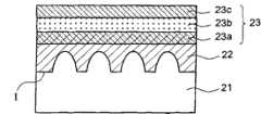
如图1A所示,首先提供经图案化的蓝宝石基板21,并在其图案化的表面上形成第三族氮化物化合物(如氮化镓,GaN)的缓冲层22,且该缓冲层22与该蓝宝石基板21的接触面为第一表面I。As shown in FIG. 1A , at first a patterned
蓝宝石基板21经图案化的实施例可参照图3(a)-(f)所示,可以采用例如角锥状、柱状、半透镜状、圆锥状等几何形状。尤其,蓝宝石基板21的图案化形状可包括锥形图案、非锥形图案、或其结合。锥形图案可包括润滑的半椭圆形(a)、棱锥形(b)、圆锥形(c)、斜截锥形(e)、斜截棱锥(f)等等,而非锥形图案例如包括柱状(d)。然本发明使用的图案不限于这些几何形状,亦可由其它形状实施。该蓝宝石基板21具有上述几何形状的突起的图案,且该第一表面I会形成对应该蓝宝石基板21的几何形状之图案,亦即,该第一表面I会形成对应的例如锥形或非锥形等几何形状的凹陷部。利用经图案化的蓝宝石基板21可以有效降低磊晶层的缺陷密度,进而提升整个发光二极管组件的使用特性。至于缓冲层22则为磊晶材料层,可通过有机金属化学气相磊晶法(MOCVD)或分子束磊晶成长法(MBE)形成在蓝宝石基板21上。The patterned
如图1B所示,接着在该缓冲层22上形成以多个磊晶材料层组成的发光层结构23,该发光层结构23可通过有机金属化学气相磊晶法(MOCVD)或分子束磊晶成长法(MBE)形成,在缓冲层22上依次形成n型氮化镓(n-GaN)层23a、发光层23b、及p型氮化镓(p-GaN)层23c。根据一实施例,发光层23b可由多量子井结构(Multiple Quantum Well,MQW)组成。As shown in FIG. 1B, a light-emitting
续如图1C所示,在该p型氮化镓(p-GaN)层23c上依次形成键结金属(bonding metal)层24,并将导电基板25以晶片键结设置在键结金属层24上。上述缓冲层、发光层、键结金属层及导电基板的形成方式可以本领域公知技术完成,因此在本说明书中不加以赘述。As shown in FIG. 1C, a bonding
续如图1D所示,由该第一表面I上将该经图案化的蓝宝石基板21移除,移除方式可利用激光剥离、蚀刻或研磨。在实施例中,优选是以激光剥离的方式,以波长248纳米(nm)的KrF准分子激光由该蓝宝石基板21侧射入,使得该缓冲层22在靠近蓝宝石基板21侧产生解离,再将组件加热至约30至40℃以将该蓝宝石基板21剥离,从而使得该第一表面I的对应该蓝宝石基板21的几何形状的图案裸露。然而,发光层所发出的光有可能因该第一表面I的图案而产生发光二极管的全内反射(total internalreflection,TIR)效应、不易离开发光二极管组件等现象。这种全内反射效应不仅降低发光二极管的发光功率,同时也会在该组件内部产生大量的热,造成组件劣化,操作特性变差。因此,本发明在移除蓝宝石基板21后将组件以酸、碱或有机溶液洗涤,进行表面平坦化处理。As shown in FIG. 1D , the patterned
如图1E所示,进行该第一表面I的平坦化步骤时,可通过选择性湿蚀刻或研磨而达成平坦化。在此实施例中,是将前述组件经清洗后浸渍在温度约20℃至200℃的蚀刻剂中,待湿蚀刻将该组件的第一表面I平坦化而形成第二表面II后,将该组件从溶液中取出,以有机溶液(如丙酮、甲醇、异丙醇或酒精)洗涤该组件。As shown in FIG. 1E , when performing the step of planarizing the first surface I, planarization can be achieved by selective wet etching or grinding. In this embodiment, the aforementioned components are cleaned and immersed in an etchant at a temperature of about 20° C. to 200° C. After the first surface I of the component is planarized by wet etching to form the second surface II, the The component is removed from the solution and the component is washed with an organic solution such as acetone, methanol, isopropanol or alcohol.
其中,该蚀刻剂对于氮化物半导体具有选择性蚀刻的特性。在一实施例中,该蚀刻剂为酸溶液,是选自硫酸(H2SO4)、磷酸(H3PO4)、硝酸(HNO3)、亚硝酸(HNO2)、亚磷酸(H3PO3)、盐酸(HCl)、醋酸(CH3COOH)、碳酸(H2CO3)、硼酸(H2BO3)、甲酸(HCOOH)、碘酸(HIO3)、草酸(H2C2O4)、氢氟酸(HF)、氢硫酸(H2S)、亚硫酸(H2SO3)、氟磺酸(HSO3F)、任何烷基磺酸(RSO3F,R=CnH2n+1)中一种或多种混合物。在另一实施例中,该蚀刻剂为碱溶液,是选自氢氧化钠(NaOH)、氢氧化钾(KOH)、氢氧化钙(Ca(OH)2)、四甲基铵氢氧化物(TMAH)、氢氧化铵(NH4OH)、碳酸钠(Na2CO3)、碳酸氢钠(NaHCO3)、碳酸钾(K2CO3)、氢氧化钡(Ba(OH)2)中的一种或多种混合物。作为该蚀刻剂的酸或碱溶液对于非平坦的氮化物蚀刻速率非常快,但对于平坦的氮化物蚀刻速率非常慢或甚至不蚀刻,因此可达到将凹凸起伏的氮化物表面平坦化的效果。值得一提的是,因具有图案的缓冲层22相对较薄,故平坦化步可能完全去除缓冲层22,而露出的第二表面II为部分n型氮化镓层23a。Wherein, the etchant has a property of selectively etching nitride semiconductors. In one embodiment, the etchant is an acid solution selected from sulfuric acid (H2 SO4 ), phosphoric acid (H3 PO4 ), nitric acid (HNO3 ), nitrous acid (HNO2 ), phosphorous acid (H3 PO3 ), hydrochloric acid (HCl), acetic acid (CH3 COOH), carbonic acid (H2 CO3 ), boric acid (H2 BO3 ), formic acid (HCOOH), iodic acid (HIO3 ), oxalic acid (H2 C2 O4 ), hydrofluoric acid (HF), hydrogen sulfuric acid (H2 S), sulfurous acid (H2 SO3 ), fluorosulfonic acid (HSO3 F), any alkylsulfonic acid (RSO3 F, R=C One or more mixtures ofn H2n+1 ). In another embodiment, the etchant is an alkaline solution selected from sodium hydroxide (NaOH), potassium hydroxide (KOH), calcium hydroxide (Ca(OH)2 ), tetramethylammonium hydroxide ( TMAH), ammonium hydroxide (NH4 OH), sodium carbonate (Na2 CO3 ), sodium bicarbonate (NaHCO3 ), potassium carbonate (K2 CO3 ), barium hydroxide (Ba(OH)2 ) One or more mixtures. The acid or alkali solution used as the etchant has a very fast etching rate for non-flat nitrides, but very slow or even no etching for flat nitrides, so the effect of flattening the uneven nitride surface can be achieved. It is worth mentioning that because the
如图1F所示,在该导电基板25的背面形成第一电极26,在该发光层结构23经平坦化后的第二表面II上(即n型氮化镓层23a上)形成第二电极27,其中第一电极26与第二电极27分别接触导电基板25与n型氮化镓层23a。从而完成本发明的垂直式发光二极管2的制备。As shown in FIG. 1F, a
由于本发明的制程,可避免发光二极管的全内反射效应、散热等不良现象。Due to the manufacturing process of the present invention, undesirable phenomena such as total internal reflection effect and heat dissipation of the light emitting diode can be avoided.
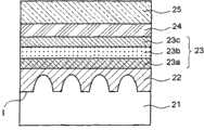
在另一实施例中,参照图2,如图1A-1F所述步骤制备垂直式发光二极管2后(即,形成第一电极26及第二电极27后),进一步粗化该发光层结构23的第二表面II,以在该第二表面II形成具有几何形状的突起物28,由此可进一步增加该发光二极管的发光效率。该突起物28的图案形状,举例但非限制,可呈角锥状、圆锥状、半透镜状等几何形状。该粗化步骤可通过化学蚀刻或干蚀刻方式进行,以在n型氮化镓层23a的表面上位于第二电极27以外的区域形成凹凸面。化学蚀刻剂选自过氧化氢(H2O2)、氢氧化钾(KOH)、四甲基铵氢氧化物(TMAH)、或上述成分的组合,例如KOH与TMAH的混合溶液,组合比例可视蚀刻条件调整。In another embodiment, referring to FIG. 2, after the vertical light-emitting
具体言之,在形成第一电极26及第二电极27后,将该组件以有机溶液洗涤以进行表面清洁,接着将组件浸渍在温度为约20℃至200℃的化学蚀刻剂中,该化学蚀刻剂为KOH与TMAH的混合溶液,该组件表面会产生不同程度的粗糙度,在第一阶段浸渍完成后取出组件,以有机溶液洗涤,再浸渍入与第一阶段相同的混合溶液进行第二阶段粗化。此处是以两阶段方式进行粗化制程。在粗化步骤完成后取出组件以有机溶液洗涤。制备得本发明的高亮度垂直式发光二极管2。Specifically, after forming the
综上所述,在本发明的制备方法中,利用经图案化的蓝宝石基板可以有效降低磊晶层的缺陷密度,进而提升整个发光二极管组件的使用特性。在此组件结构中,由于晶片键结导电基板与激光剥离蓝宝石基板,使得原本位于靠近蓝宝石基板的底层翻转成为组件的上表面,因此使得对应蓝宝石基板图案所形成的图案在上表面成为凹陷部(参照图1C及1D)。然而,如图1D所示的几何结构,将使发光层所发出的光产生全内反射(total internalreflection,TIR)效应而不易离开发光二极管组件。该全内反射效应不仅降低发光二极管的发光功率,同时也会在该组件内部产生大量的热,造成组件劣化,操作特性变差。因此,本发明的方法在于蓝宝石基板剥离后,以平坦化步骤来解决此问题,并克服上述组件劣化及操作特性变差的缺点。To sum up, in the preparation method of the present invention, using the patterned sapphire substrate can effectively reduce the defect density of the epitaxial layer, thereby improving the service characteristics of the entire light emitting diode assembly. In this component structure, due to the bonding of the wafer to the conductive substrate and the laser lift-off of the sapphire substrate, the bottom layer originally located close to the sapphire substrate is turned over to become the upper surface of the component, so that the pattern formed corresponding to the pattern of the sapphire substrate becomes a depression on the upper surface ( See Figures 1C and 1D). However, the geometric structure shown in FIG. 1D will cause the light emitted by the light-emitting layer to produce a total internal reflection (TIR) effect and not easily leave the light-emitting diode assembly. The total internal reflection effect not only reduces the luminous power of the LED, but also generates a large amount of heat inside the component, causing the component to deteriorate and the operating characteristics to deteriorate. Therefore, the method of the present invention solves this problem by using a planarization step after the sapphire substrate is peeled off, and overcomes the above-mentioned shortcomings of component degradation and poor operation characteristics.
然而,为了进一步提升发光二极管的发光效率,本发明针对发光二极管表面进行粗化步骤,制作角锥状、圆锥状、或半透镜状的突起物28,根据这些突起物的大小以及数目,该LED组件的发光功率可提升至少5%到10%。根据本发明一实施例,突起物28的形状也可以图3所示的不同形状实现,同样可提升发光二极管的发光效率。However, in order to further improve the luminous efficiency of the light-emitting diode, the present invention performs a roughening step on the surface of the light-emitting diode to make pyramid-shaped, conical, or semi-lens-shaped
附图说明Description of drawings
图1A-1F说明本发明制造高亮度垂直式发光二极管的方法的一实施例。1A-1F illustrate an embodiment of the method of manufacturing a high-brightness vertical light-emitting diode of the present invention.
图2说明本发明制造高亮度垂直式发光二极管的方法的另一实施例。FIG. 2 illustrates another embodiment of the method of manufacturing a high-brightness vertical LED according to the present invention.
图3绘示经图案化的实施例。Figure 3 illustrates a patterned embodiment.
主要组件符号说明Explanation of main component symbols
2 高亮度垂直式发光二极管2 high brightness vertical light emitting diodes
21 蓝宝石基板21 Sapphire substrate
22 缓冲层22 buffer layer
23 发光层结构23 Light-emitting layer structure
23a n-GaN层23a n-GaN layer
23b 发光层23b luminous layer
23c p-GaN层23c p-GaN layer
24 键结金属层24 bonding metal layer
25 导电基板25 Conductive substrate
26 第一电极26 first electrode
27 第二电极27 second electrode
28 突起物28 protrusions
I 第一表面I first surface
II 第二表面II Second Surface
Claims (13)
Priority Applications (1)
| Application Number | Priority Date | Filing Date | Title |
|---|---|---|---|
| CN2010105093269ACN102447020A (en) | 2010-10-12 | 2010-10-12 | Method for manufacturing high-brightness vertical light-emitting diodes |
Applications Claiming Priority (1)
| Application Number | Priority Date | Filing Date | Title |
|---|---|---|---|
| CN2010105093269ACN102447020A (en) | 2010-10-12 | 2010-10-12 | Method for manufacturing high-brightness vertical light-emitting diodes |
Publications (1)
| Publication Number | Publication Date |
|---|---|
| CN102447020Atrue CN102447020A (en) | 2012-05-09 |
Family
ID=46009327
Family Applications (1)
| Application Number | Title | Priority Date | Filing Date |
|---|---|---|---|
| CN2010105093269APendingCN102447020A (en) | 2010-10-12 | 2010-10-12 | Method for manufacturing high-brightness vertical light-emitting diodes |
Country Status (1)
| Country | Link |
|---|---|
| CN (1) | CN102447020A (en) |
Cited By (4)
| Publication number | Priority date | Publication date | Assignee | Title |
|---|---|---|---|---|
| WO2015154551A1 (en)* | 2014-04-08 | 2015-10-15 | 厦门市三安光电科技有限公司 | High-brightness light-emitting diode having surface microstructure, and preparation and screening method therefor |
| CN105374906A (en)* | 2014-08-26 | 2016-03-02 | 广东量晶光电科技有限公司 | LED chip and preparation method thereof |
| CN106206874A (en)* | 2016-08-12 | 2016-12-07 | 泉州市三星消防设备有限公司 | A kind of electrode aberration ameliorative way of LED chip based on roughening epitaxial wafer |
| CN107104040A (en)* | 2016-02-23 | 2017-08-29 | 北京大学 | The anode fabrication method of gallium nitride Schottky diode |
Citations (2)
| Publication number | Priority date | Publication date | Assignee | Title |
|---|---|---|---|---|
| US20030082893A1 (en)* | 2001-07-02 | 2003-05-01 | Osamu Matsumoto | Method of fabricating nitride semiconductor and method of fabricating semiconductor device |
| US7781242B1 (en)* | 2009-12-10 | 2010-08-24 | Walsin Lihwa Corporation | Method of forming vertical structure light emitting diode with heat exhaustion structure |
- 2010
- 2010-10-12CNCN2010105093269Apatent/CN102447020A/enactivePending
Patent Citations (2)
| Publication number | Priority date | Publication date | Assignee | Title |
|---|---|---|---|---|
| US20030082893A1 (en)* | 2001-07-02 | 2003-05-01 | Osamu Matsumoto | Method of fabricating nitride semiconductor and method of fabricating semiconductor device |
| US7781242B1 (en)* | 2009-12-10 | 2010-08-24 | Walsin Lihwa Corporation | Method of forming vertical structure light emitting diode with heat exhaustion structure |
Cited By (5)
| Publication number | Priority date | Publication date | Assignee | Title |
|---|---|---|---|---|
| WO2015154551A1 (en)* | 2014-04-08 | 2015-10-15 | 厦门市三安光电科技有限公司 | High-brightness light-emitting diode having surface microstructure, and preparation and screening method therefor |
| US10249791B2 (en) | 2014-04-08 | 2019-04-02 | Xiamen Sanan Optoelectronics Technology Co., Ltd. | High-brightness light-emitting diode with surface microstructures |
| CN105374906A (en)* | 2014-08-26 | 2016-03-02 | 广东量晶光电科技有限公司 | LED chip and preparation method thereof |
| CN107104040A (en)* | 2016-02-23 | 2017-08-29 | 北京大学 | The anode fabrication method of gallium nitride Schottky diode |
| CN106206874A (en)* | 2016-08-12 | 2016-12-07 | 泉州市三星消防设备有限公司 | A kind of electrode aberration ameliorative way of LED chip based on roughening epitaxial wafer |
Similar Documents
| Publication | Publication Date | Title |
|---|---|---|
| US20230275185A1 (en) | Highly efficient gallium nitride based light emitting diodes via surface roughening | |
| US9041005B2 (en) | Solid state lighting devices with cellular arrays and associated methods of manufacturing | |
| CN104993023B (en) | A kind of method that method using chemical attack removes growth substrates | |
| TWI405257B (en) | Method of separating substrate and semiconductor layer | |
| TW201216503A (en) | Method for fabricating a vertical light-emitting diode with high brightness | |
| CN102544248B (en) | Manufacturing method for light emitting diode grain | |
| JP5191866B2 (en) | Semiconductor light emitting device manufacturing method and semiconductor light emitting device | |
| CN101494267A (en) | Method for manufacturing gallium nitride-based light-emitting device based on substrate stripping | |
| CN102117869A (en) | Method for stripping substrate of LED | |
| JP2010123717A (en) | Semiconductor light emitting element and method for manufacturing it | |
| CN106711291A (en) | LED vertical chip structure and manufacturing method thereof | |
| Lee et al. | Enhancement of InGaN-based vertical LED with concavely patterned surface using patterned sapphire substrate | |
| JP2004200639A (en) | Method of manufacturing light emitting diode element and light emitting diode element | |
| CN110071198A (en) | A kind of light-emitting component and preparation method thereof, array substrate | |
| CN102447020A (en) | Method for manufacturing high-brightness vertical light-emitting diodes | |
| CN102569556B (en) | There is light-emitting diode and the manufacture method of high enabling n-type ohmic contact | |
| JP5702165B2 (en) | High efficiency gallium nitride based light emitting diodes by surface roughening | |
| KR100752348B1 (en) | Vertical structure light emitting diode manufacturing method | |
| CN112968085A (en) | Epitaxial wafer manufacturing method, chip manufacturing method and chip | |
| RU2819047C1 (en) | Light-emitting diode | |
| US8536585B2 (en) | Semiconductor light emitting device including anode and cathode having the same metal structure | |
| JP2006135222A (en) | Etching method and semiconductor device manufacturing method | |
| TW201228024A (en) | Method for making light emitting diode chip | |
| TW201517303A (en) | Method for manufacturing vertical-feedthrough LED |
Legal Events
| Date | Code | Title | Description |
|---|---|---|---|
| C06 | Publication | ||
| PB01 | Publication | ||
| C10 | Entry into substantive examination | ||
| SE01 | Entry into force of request for substantive examination | ||
| C02 | Deemed withdrawal of patent application after publication (patent law 2001) | ||
| WD01 | Invention patent application deemed withdrawn after publication | Application publication date:20120509 |