CN102445800A - Liquid crystal display device - Google Patents
Liquid crystal display deviceDownload PDFInfo
- Publication number
- CN102445800A CN102445800ACN2011103070464ACN201110307046ACN102445800ACN 102445800 ACN102445800 ACN 102445800ACN 2011103070464 ACN2011103070464 ACN 2011103070464ACN 201110307046 ACN201110307046 ACN 201110307046ACN 102445800 ACN102445800 ACN 102445800A
- Authority
- CN
- China
- Prior art keywords
- liquid crystal
- display device
- crystal display
- electrode
- common electrode
- Prior art date
- Legal status (The legal status is an assumption and is not a legal conclusion. Google has not performed a legal analysis and makes no representation as to the accuracy of the status listed.)
- Granted
Links
Images


Classifications
- G—PHYSICS
- G02—OPTICS
- G02F—OPTICAL DEVICES OR ARRANGEMENTS FOR THE CONTROL OF LIGHT BY MODIFICATION OF THE OPTICAL PROPERTIES OF THE MEDIA OF THE ELEMENTS INVOLVED THEREIN; NON-LINEAR OPTICS; FREQUENCY-CHANGING OF LIGHT; OPTICAL LOGIC ELEMENTS; OPTICAL ANALOGUE/DIGITAL CONVERTERS
- G02F1/00—Devices or arrangements for the control of the intensity, colour, phase, polarisation or direction of light arriving from an independent light source, e.g. switching, gating or modulating; Non-linear optics
- G02F1/01—Devices or arrangements for the control of the intensity, colour, phase, polarisation or direction of light arriving from an independent light source, e.g. switching, gating or modulating; Non-linear optics for the control of the intensity, phase, polarisation or colour
- G02F1/13—Devices or arrangements for the control of the intensity, colour, phase, polarisation or direction of light arriving from an independent light source, e.g. switching, gating or modulating; Non-linear optics for the control of the intensity, phase, polarisation or colour based on liquid crystals, e.g. single liquid crystal display cells
- G02F1/133—Constructional arrangements; Operation of liquid crystal cells; Circuit arrangements
- G02F1/1333—Constructional arrangements; Manufacturing methods
- G02F1/1343—Electrodes
- G02F1/134309—Electrodes characterised by their geometrical arrangement
- G02F1/134363—Electrodes characterised by their geometrical arrangement for applying an electric field parallel to the substrate, i.e. in-plane switching [IPS]
- G—PHYSICS
- G02—OPTICS
- G02F—OPTICAL DEVICES OR ARRANGEMENTS FOR THE CONTROL OF LIGHT BY MODIFICATION OF THE OPTICAL PROPERTIES OF THE MEDIA OF THE ELEMENTS INVOLVED THEREIN; NON-LINEAR OPTICS; FREQUENCY-CHANGING OF LIGHT; OPTICAL LOGIC ELEMENTS; OPTICAL ANALOGUE/DIGITAL CONVERTERS
- G02F1/00—Devices or arrangements for the control of the intensity, colour, phase, polarisation or direction of light arriving from an independent light source, e.g. switching, gating or modulating; Non-linear optics
- G02F1/01—Devices or arrangements for the control of the intensity, colour, phase, polarisation or direction of light arriving from an independent light source, e.g. switching, gating or modulating; Non-linear optics for the control of the intensity, phase, polarisation or colour
- G02F1/13—Devices or arrangements for the control of the intensity, colour, phase, polarisation or direction of light arriving from an independent light source, e.g. switching, gating or modulating; Non-linear optics for the control of the intensity, phase, polarisation or colour based on liquid crystals, e.g. single liquid crystal display cells
- G02F1/133—Constructional arrangements; Operation of liquid crystal cells; Circuit arrangements
- G02F1/1333—Constructional arrangements; Manufacturing methods
- G02F1/13338—Input devices, e.g. touch panels
- G—PHYSICS
- G02—OPTICS
- G02F—OPTICAL DEVICES OR ARRANGEMENTS FOR THE CONTROL OF LIGHT BY MODIFICATION OF THE OPTICAL PROPERTIES OF THE MEDIA OF THE ELEMENTS INVOLVED THEREIN; NON-LINEAR OPTICS; FREQUENCY-CHANGING OF LIGHT; OPTICAL LOGIC ELEMENTS; OPTICAL ANALOGUE/DIGITAL CONVERTERS
- G02F1/00—Devices or arrangements for the control of the intensity, colour, phase, polarisation or direction of light arriving from an independent light source, e.g. switching, gating or modulating; Non-linear optics
- G02F1/01—Devices or arrangements for the control of the intensity, colour, phase, polarisation or direction of light arriving from an independent light source, e.g. switching, gating or modulating; Non-linear optics for the control of the intensity, phase, polarisation or colour
- G02F1/13—Devices or arrangements for the control of the intensity, colour, phase, polarisation or direction of light arriving from an independent light source, e.g. switching, gating or modulating; Non-linear optics for the control of the intensity, phase, polarisation or colour based on liquid crystals, e.g. single liquid crystal display cells
- G02F1/133—Constructional arrangements; Operation of liquid crystal cells; Circuit arrangements
- G02F1/1333—Constructional arrangements; Manufacturing methods
- G02F1/1339—Gaskets; Spacers; Sealing of cells
- G—PHYSICS
- G02—OPTICS
- G02F—OPTICAL DEVICES OR ARRANGEMENTS FOR THE CONTROL OF LIGHT BY MODIFICATION OF THE OPTICAL PROPERTIES OF THE MEDIA OF THE ELEMENTS INVOLVED THEREIN; NON-LINEAR OPTICS; FREQUENCY-CHANGING OF LIGHT; OPTICAL LOGIC ELEMENTS; OPTICAL ANALOGUE/DIGITAL CONVERTERS
- G02F1/00—Devices or arrangements for the control of the intensity, colour, phase, polarisation or direction of light arriving from an independent light source, e.g. switching, gating or modulating; Non-linear optics
- G02F1/01—Devices or arrangements for the control of the intensity, colour, phase, polarisation or direction of light arriving from an independent light source, e.g. switching, gating or modulating; Non-linear optics for the control of the intensity, phase, polarisation or colour
- G02F1/13—Devices or arrangements for the control of the intensity, colour, phase, polarisation or direction of light arriving from an independent light source, e.g. switching, gating or modulating; Non-linear optics for the control of the intensity, phase, polarisation or colour based on liquid crystals, e.g. single liquid crystal display cells
- G02F1/133—Constructional arrangements; Operation of liquid crystal cells; Circuit arrangements
- G02F1/1333—Constructional arrangements; Manufacturing methods
- G02F1/1343—Electrodes
- G—PHYSICS
- G06—COMPUTING OR CALCULATING; COUNTING
- G06F—ELECTRIC DIGITAL DATA PROCESSING
- G06F3/00—Input arrangements for transferring data to be processed into a form capable of being handled by the computer; Output arrangements for transferring data from processing unit to output unit, e.g. interface arrangements
- G06F3/01—Input arrangements or combined input and output arrangements for interaction between user and computer
- G06F3/03—Arrangements for converting the position or the displacement of a member into a coded form
- G06F3/041—Digitisers, e.g. for touch screens or touch pads, characterised by the transducing means
- G06F3/0412—Digitisers structurally integrated in a display
- G—PHYSICS
- G06—COMPUTING OR CALCULATING; COUNTING
- G06F—ELECTRIC DIGITAL DATA PROCESSING
- G06F3/00—Input arrangements for transferring data to be processed into a form capable of being handled by the computer; Output arrangements for transferring data from processing unit to output unit, e.g. interface arrangements
- G06F3/01—Input arrangements or combined input and output arrangements for interaction between user and computer
- G06F3/03—Arrangements for converting the position or the displacement of a member into a coded form
- G06F3/041—Digitisers, e.g. for touch screens or touch pads, characterised by the transducing means
- G06F3/044—Digitisers, e.g. for touch screens or touch pads, characterised by the transducing means by capacitive means
- G06F3/0443—Digitisers, e.g. for touch screens or touch pads, characterised by the transducing means by capacitive means using a single layer of sensing electrodes
- G—PHYSICS
- G02—OPTICS
- G02F—OPTICAL DEVICES OR ARRANGEMENTS FOR THE CONTROL OF LIGHT BY MODIFICATION OF THE OPTICAL PROPERTIES OF THE MEDIA OF THE ELEMENTS INVOLVED THEREIN; NON-LINEAR OPTICS; FREQUENCY-CHANGING OF LIGHT; OPTICAL LOGIC ELEMENTS; OPTICAL ANALOGUE/DIGITAL CONVERTERS
- G02F1/00—Devices or arrangements for the control of the intensity, colour, phase, polarisation or direction of light arriving from an independent light source, e.g. switching, gating or modulating; Non-linear optics
- G02F1/01—Devices or arrangements for the control of the intensity, colour, phase, polarisation or direction of light arriving from an independent light source, e.g. switching, gating or modulating; Non-linear optics for the control of the intensity, phase, polarisation or colour
- G02F1/13—Devices or arrangements for the control of the intensity, colour, phase, polarisation or direction of light arriving from an independent light source, e.g. switching, gating or modulating; Non-linear optics for the control of the intensity, phase, polarisation or colour based on liquid crystals, e.g. single liquid crystal display cells
- G02F1/133—Constructional arrangements; Operation of liquid crystal cells; Circuit arrangements
- G02F1/136—Liquid crystal cells structurally associated with a semi-conducting layer or substrate, e.g. cells forming part of an integrated circuit
- G02F1/1362—Active matrix addressed cells
- G02F1/136209—Light shielding layers, e.g. black matrix, incorporated in the active matrix substrate, e.g. structurally associated with the switching element
Landscapes
- Physics & Mathematics (AREA)
- Engineering & Computer Science (AREA)
- Nonlinear Science (AREA)
- General Physics & Mathematics (AREA)
- Theoretical Computer Science (AREA)
- General Engineering & Computer Science (AREA)
- Crystallography & Structural Chemistry (AREA)
- Optics & Photonics (AREA)
- Chemical & Material Sciences (AREA)
- Mathematical Physics (AREA)
- Human Computer Interaction (AREA)
- Liquid Crystal (AREA)
- Geometry (AREA)
Abstract
Translated fromChineseDescription
Translated fromChinese本申请主张2010年10月8日提交的韩国专利申请No.10-2010-0098256的优先权,在此援引该专利申请加入本文,如同在此完全阐述一样。This application claims priority to Korean Patent Application No. 10-2010-0098256 filed on October 8, 2010, which is hereby incorporated by reference as if fully set forth herein.
技术领域technical field
本发明涉及一种液晶显示器件,尤其涉及一种设有用于感测使用者触摸的感测电极的液晶显示器件。The present invention relates to a liquid crystal display device, in particular to a liquid crystal display device provided with a sensing electrode for sensing a user's touch.
背景技术Background technique
由于基于低驱动电压的低功耗以及便携性的优点,液晶显示器件被广泛用于笔记本电脑、显示器、航天器、飞行器等多种领域中。Due to the advantages of low power consumption and portability based on low driving voltage, liquid crystal display devices are widely used in various fields such as notebook computers, displays, spacecraft, and aircraft.
液晶显示器件包括下基板、上基板、以及形成在上下基板之间的液晶层。在液晶显示器件中,根据是否施加电场来控制液晶层中液晶分子的排列状态,并根据液晶分子的排列状态来控制透光率,由此在其上显示图像。A liquid crystal display device includes a lower substrate, an upper substrate, and a liquid crystal layer formed between the upper and lower substrates. In a liquid crystal display device, an alignment state of liquid crystal molecules in a liquid crystal layer is controlled according to whether an electric field is applied, and light transmittance is controlled according to the alignment state of the liquid crystal molecules, thereby displaying an image thereon.
通常使用鼠标或键盘作为液晶显示器件的输入部件。而允许使用者利用手指或笔直接输入信息的触摸屏被主要应用于导航系统、便携式终端和家用电器。Usually a mouse or a keyboard is used as the input part of the liquid crystal display device. And touch screens that allow users to directly input information using fingers or pens are mainly used in navigation systems, portable terminals, and home appliances.
下文,将参照附图描述现有技术的设有触摸屏的液晶显示器件。Hereinafter, a related art liquid crystal display device provided with a touch screen will be described with reference to the accompanying drawings.
图1是图解现有技术的液晶显示器件的剖面图。FIG. 1 is a sectional view illustrating a related art liquid crystal display device.
如图1中所示,现有技术的液晶显示器件包括液晶面板10和触摸屏20。As shown in FIG. 1 , a related art liquid crystal display device includes a
液晶面板10显示图像,并包括下基板12、上基板14、以及形成在下基板12和上基板14之间的液晶层16。The
触摸屏20形成在液晶面板10上以感测使用者的触摸,触摸屏20包括触摸基板22、形成在触摸基板22之下的第一感测电极24、以及形成在触摸基板22之上的第二感测电极26。The
第一感测电极24在水平方向上布置在触摸基板22之下,而第二感测电极26在垂直方向上布置在触摸基板22之上。因此,如果使用者触摸预定位置,则在触摸位置处第一感测电极24与第二感测电极26之间的电容发生变化。结果,感测到电容发生变化的位置,由此可感测使用者的触摸位置。The
然而,在前述现有技术的液晶显示器件中,因为触摸屏20单独地形成在液晶面板10上,所以触摸屏20增加了液晶显示器件的整体厚度。由于该原因,产生了制造工艺步骤复杂且制造成本增加的问题。However, in the aforementioned related art liquid crystal display device, since the
发明内容Contents of the invention
本发明涉及一种液晶显示器件,其基本上克服了由于现有技术的限制和缺点而导致的一个或多个问题。The present invention is directed to a liquid crystal display device that substantially overcomes one or more of the problems due to limitations and disadvantages of the related art.
本发明的一个优点是提供一种液晶显示器件,其中用于感测使用者触摸的感测电极内嵌在液晶面板中从而不需要在液晶面板上的单独的触摸屏,由此减小了液晶显示器件的整体厚度,简化了制造工艺步骤并降低了制造成本。An advantage of the present invention is to provide a liquid crystal display device in which sensing electrodes for sensing a user's touch are embedded in a liquid crystal panel so as not to require a separate touch screen on the liquid crystal panel, thereby reducing the size of the liquid crystal display. The overall thickness of the device simplifies the manufacturing process steps and reduces the manufacturing cost.
在下面的描述中将列出本发明的其它特征和优点,这些特征和优点的一部分将通过所述描述显而易见的,或者可通过本发明的实施领会到。通过说明书、权利要求以及附图中特别指出的结构可实现和获得本发明的这些以及其他优点。Additional features and advantages of the invention will be set forth in the description which follows, and in part will be apparent from the description, or may be learned by practice of the invention. These and other advantages of the invention will be realized and attained by the structure particularly pointed out in the written description, claims hereof as well as the appended drawings.
为了获得这些以及其他优点并且根据本发明的目的,如这里具体表示和广义描述的,一种液晶显示器件,包括第一基板和第二基板;在所述第一基板上布置成彼此交叉以限定像素区域的栅线和数据线;形成在所述像素区域中的像素电极;与所述像素电极一起形成电场并感测使用者触摸的公共电极;和形成在所述第二基板上用于遮蔽向除所述像素区域之外的其他区域的光泄漏的遮光层;形成在所述遮光层上用于保持盒间隙的柱状衬垫料;和形成在所述柱状衬垫料上并与所述公共电极电连接的感测线。To achieve these and other advantages and in accordance with the purpose of the present invention, as embodied and broadly described herein, a liquid crystal display device comprises a first substrate and a second substrate; A gate line and a data line in a pixel area; a pixel electrode formed in the pixel area; a common electrode forming an electric field with the pixel electrode and sensing a user's touch; and a shielding electrode formed on the second substrate a light-shielding layer for light leakage to areas other than the pixel area; a columnar spacer formed on the light-shielding layer for maintaining a cell gap; and a columnar spacer formed on the columnar spacer and connected to the The sensing line to which the common electrode is electrically connected.
应当理解,本发明前面的一般性描述和下面的详细描述都是例示性的和解释性的,意在对要求保护的内容提供进一步的解释。It is to be understood that both the foregoing general description and the following detailed description of the invention are exemplary and explanatory and are intended to provide further explanation of what is claimed.
附图说明Description of drawings
附图向本发明提供进一步理解并组成说明书一部分,其图解了本发明的实施方式并与说明书一起用于解释本发明的原理。在附图中:The accompanying drawings, which are included to provide a further understanding of the invention and constitute a part of this specification, illustrate embodiments of the invention and together with the description serve to explain the principles of the invention. In the attached picture:
图1是图解现有技术的液晶显示器件的剖面图;1 is a sectional view illustrating a prior art liquid crystal display device;
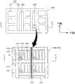
图2a是图解本发明第一个实施方式的液晶显示器件的下基板的平面图,图2b是沿图2a的线A-A的剖面图,图2c是图解本发明第一个实施方式的液晶显示器件的上基板的平面图,图2d是沿图2a的线B-B的剖面图,图2e是图解本发明第一个实施方式的液晶显示器件沿图2a和图2c的线C-C的剖面图;2a is a plan view illustrating the lower substrate of the liquid crystal display device of the first embodiment of the present invention, FIG. 2b is a cross-sectional view along the line A-A of FIG. 2a, and FIG. 2c is a plan view of the liquid crystal display device of the first embodiment of the present invention A plan view of the upper substrate, Fig. 2d is a sectional view along the line B-B of Fig. 2a, and Fig. 2e is a sectional view illustrating the liquid crystal display device according to the first embodiment of the present invention along the line C-C of Fig. 2a and Fig. 2c;
图3a是图解本发明第二个实施方式的液晶显示器件的下基板的平面图,图3b是图解本发明第二个实施方式的液晶显示器件的上基板的平面图,图3c是图解本发明第二个实施方式的液晶显示器件沿图3a和图3b的线C-C的剖面图;3a is a plan view illustrating a lower substrate of a liquid crystal display device according to a second embodiment of the present invention, FIG. 3b is a plan view illustrating an upper substrate of a liquid crystal display device according to a second embodiment of the present invention, and FIG. A sectional view of the liquid crystal display device of the first embodiment along the line C-C of Fig. 3a and Fig. 3b;
图4a是图解本发明第三个实施方式的液晶显示器件的下基板的平面图,图4b是图解本发明第三个实施方式的液晶显示器件的上基板的平面图,图4c是图解本发明第三个实施方式的液晶显示器件沿图4a和图4b的线C-C的剖面图;4a is a plan view illustrating a lower substrate of a liquid crystal display device according to a third embodiment of the present invention, FIG. 4b is a plan view illustrating an upper substrate of a liquid crystal display device according to a third embodiment of the present invention, and FIG. A sectional view of the liquid crystal display device of the first embodiment along the line C-C of Fig. 4a and Fig. 4b;
图5a是图解本发明第四个实施方式的液晶显示器件的下基板的平面图,图5b是图解本发明第四个实施方式的液晶显示器件的上基板的平面图,图5c是图解本发明第四个实施方式的液晶显示器件沿图5a和图5b的线C-C的剖面图。5 a is a plan view illustrating a lower substrate of a liquid crystal display device according to a fourth embodiment of the present invention, FIG. 5 b is a plan view illustrating an upper substrate of a liquid crystal display device according to a fourth embodiment of the present invention, and FIG. 5 c is a plan view illustrating a fourth embodiment of the present invention. A cross-sectional view of the liquid crystal display device of the first embodiment along the line C-C of FIG. 5a and FIG. 5b.
具体实施方式Detailed ways
现在将详细描述本发明典型的实施方式,附图中图解了这些实施方式的一些例子。尽可能地,在整个附图中使用相同的附图标记表示相同或相似的部件。Reference will now be made in detail to exemplary embodiments of the present invention, examples of which are illustrated in the accompanying drawings. Wherever possible, the same reference numbers will be used throughout the drawings to refer to the same or like parts.
图2a是图解根据本发明第一个实施方式的液晶显示器件的下基板的平面图,图2b是沿图2a的线A-A的剖面图,图2c是图解根据本发明第一个实施方式的液晶显示器件的上基板的平面图,图2d是沿图2a的线B-B的剖面图,图2e是图解根据本发明第一个实施方式的液晶显示器件沿图2a和图2c的线C-C的剖面图。2a is a plan view illustrating a lower substrate of a liquid crystal display device according to a first embodiment of the present invention, FIG. 2b is a cross-sectional view along line A-A of FIG. 2a, and FIG. 2c is a plan view illustrating a liquid crystal display device according to a first embodiment of the present invention A plan view of the upper substrate of the device, Figure 2d is a sectional view along the line B-B of Figure 2a, and Figure 2e is a sectional view illustrating the liquid crystal display device according to the first embodiment of the present invention along the line C-C of Figure 2a and Figure 2c.
参照图2a,尤其是用箭头标记的部分放大图,根据本发明第一个实施方式的液晶显示器件包括第一基板100、栅线110、数据线120、薄膜晶体管T、像素电极130和公共电极140。Referring to FIG. 2a, especially the partially enlarged view marked with arrows, the liquid crystal display device according to the first embodiment of the present invention includes a
栅线110以第一方向,例如X轴方向布置在基板100上,数据线120以第二方向,例如Y轴方向布置在基板100上。这样,栅线110和数据线120彼此交叉以限定出多个像素区域。尽管栅线110和数据线120如所示布置成直线,但它们可以布置成曲线。The gate lines 110 are arranged on the
薄膜晶体管T为开关元件并形成在栅线110和数据线120彼此交叉的区域中。薄膜晶体管T包括栅电极112、半导体层117、源电极122和漏电极124。栅电极112从栅线110伸出,源电极122从数据线120伸出,而漏电极124面对源电极122。The thin film transistor T is a switching element and is formed in a region where the
前述薄膜晶体管T可具有多种结构,例如栅电极112形成在半导体层117下的底栅结构以及栅电极112形成在半导体层117上的顶栅结构。此外,可对各个电极的类型进行多种修改。The aforementioned thin film transistor T may have various structures, such as a bottom gate structure in which the
像素电极130形成在每个像素区域中并与薄膜晶体管T的漏电极124电连接。特别地,尽管像素电极130可与漏电极124直接连接,但并不限于上面的例子。The
公共电极140用于通过与像素电极130一起形成电场来驱动液晶层。特别地,公共电极140在像素区域中包括一个或多个狭缝145。因此,通过狭缝145在像素电极130与公共电极140之间形成了边缘电场,并且可通过该边缘电场来驱动液晶。The
图2b对应于像素区域在垂直方向上的剖面。如图2b中所示,在第一基板100上形成有栅电极112,在栅电极112上形成有栅绝缘膜115。此外,在栅绝缘膜115上形成有半导体层117,在半导体层17上形成有彼此面对的源电极122和漏电极124。Figure 2b corresponds to a cross section of the pixel area in the vertical direction. As shown in FIG. 2 b , a
像素电极130形成在漏电极124上。这样,漏电极124和像素电极130彼此直接连接。同时,尽管像素电极130可如图所示延伸到漏电极124的上表面,但像素电极130也可延伸到漏电极124的下表面。The
在像素电极130上形成有钝化膜125,并且公共电极140形成在钝化膜125上。A
因为公共电极140包括一个或多个狭缝145,所以可通过狭缝145在像素电极130与公共电极140之间形成边缘电场。Since the
同时,公共电极140如上所述用于通过与像素电极130一起形成电场来驱动液晶,并还用作感测使用者触摸位置的感测电极。为了用作感测电极,公共电极140并不形成在基板100的整个表面上,而是以预定图案形成。Meanwhile, the
换言之,如图2a中所示,公共电极140包括多个第一公共电极141和多个第二公共电极142。此时,可通过第一公共电极141感测使用者触摸的Y轴位置,并可通过第二公共电极142感测使用者触摸的X轴位置。In other words, as shown in FIG. 2 a , the
可考虑手指或笔的触摸表面而适当地形成第一公共电极141和第二公共电极142的尺寸。例如,第一公共电极141可形成为包括几十个像素或几百个像素。The sizes of the first
下面,将更加详细地描述用作感测电极的第一公共电极141和第二公共电极142。Hereinafter, the first
首先,为了感测使用者触摸的X轴位置,多个第二公共电极142在X轴方向上以预定间隔彼此隔开。此外,第二公共电极142在Y轴方向上纵向地形成。First, in order to sense the X-axis position touched by the user, the plurality of second
因此,如果使用者触摸预定位置,则在多个第二公共电极142之中电容发生变化的第二公共电极142被识别出来。结果,能感测出使用者触摸的X轴位置。Accordingly, if the user touches a predetermined position, the second
接着,为了感测使用者触摸的Y轴位置,多个第一公共电极141在Y轴方向上以预定间隔彼此隔开。然而,如果第一公共电极141在X轴方向上纵向地形成,那么第一公共电极141和第二公共电极142彼此电连接,由此将不能感测出使用者触摸的X轴和Y轴位置。因此,第一公共电极141不在X轴方向上纵向地形成,而是在X轴方向上以预定间隔彼此隔开。换言之,如图所示,第二公共电极142在X轴方向上形成在第一公共电极141之间,而第二公共电极142在Y轴方向上并不形成在第一公共电极141之间。Next, in order to sense the Y-axis position touched by the user, the plurality of first
因为如上所述通过在多个第一公共电极141之间插入第二公共电极142而使多个第一公共电极141在X轴方向上以预定间隔彼此隔开,所以需要将所述多个第一公共电极141彼此电连接。在X轴方向上布置的第一公共电极141的电连接将通过形成在上基板200中的感测线250实现,这将在后面描述。Since the plurality of first
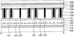
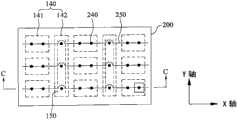
参照图2c,特别是由箭头标记的部分放大图和图2d,根据本发明第一个实施方式的液晶显示器件的上基板包括第二基板200、遮光层210、滤色器层220、涂层230、柱状衬垫料240和感测线250。Referring to FIG. 2c, especially the partially enlarged view marked by the arrow and FIG. 2d, the upper substrate of the liquid crystal display device according to the first embodiment of the present invention includes a
遮光层210用于遮蔽光泄漏到除像素区域之外的其他区域,并以矩阵方式形成在第二基板200上。The
滤色器层220形成在遮光层210之间并包括红色R、绿色G和蓝色B的滤色器。The
涂层230形成在滤色器层220上并用于使基板表面平坦。The
柱状衬垫料240形成在涂层230上并用于保持液晶显示器件的盒间隙。柱状衬垫料240形成在与遮光层210对应的区域中,以防止透光率下降。A
如上所述,感测线250用于将形成在液晶显示器件的第一基板100上的第一公共电极141彼此电连接。As described above, the
在图2c中,液晶显示器件的第一基板100的元件由虚线表示。参照图2c,感测线250在X方向上延伸,以将第一公共电极141彼此电连接。In Fig. 2c, elements of the
因此,如果使用者触摸预定位置,则感测线250识别出在多个第一公共电极141之中电容发生变化的第一公共电极141。结果,能感测出使用者触摸的Y轴位置。Accordingly, if a user touches a predetermined position, the
同时,尽管感测线250用于将在X轴方向上布置的第一公共电极141彼此电连接,但由于感测线250,第一公共电极141不应与第二公共电极142电连接。因此,尽管感测线250与第一公共电极141电连接,但其不与第二公共电极142电连接。Meanwhile, although the
更详细地,感测线250通过柱状衬垫料240与公共电极140连接。为此,尽管柱状衬垫料240形成在第一公共电极141中有感测线250经过的区域中,但其并未形成在感测线250经过的第二公共电极的区域中。因此,感测线250通过柱状衬垫料240与第一公共电极141电连接,但感测线250不与第二公共电极142电连接。In more detail, the
参照图2e将更容易理解通过柱状衬垫料240将感测线250与第一公共电极141电连接的方法。A method of electrically connecting the
图2e对应于图2a的栅线110以及图2c的遮光层的区域在垂直方向上的剖面。如图2e中所示,栅线110形成在第一基板100上,在栅线110上形成有栅绝缘膜115。此外,数据线120以预定间隔形成在栅绝缘膜115上,在数据线120上形成有钝化膜125。此外,在钝化膜125上交替地形成有第一公共电极141和第二公共电极142。FIG. 2e corresponds to the vertical section of the
此外,遮光层210形成在第二基板200上,滤色器层220形成在遮光层210上。涂层230形成在滤色器层220上,柱状衬垫料240形成在涂层230上,且感测线250形成在柱状衬垫料240上。In addition, a
此时,因为柱状衬垫料240形成在与第一公共电极141对应的区域中,所以形成在柱状衬垫料240上的感测线250与第一公共电极141电连接,但不与第二公共电极142电连接。At this time, since the
再次参照图2c,尽管如图所示一条感测线250与第一公共电极141连接,但多条感测线250可与第一公共电极141连接。特别是,因为通常使用具有高电阻的透明导电氧化物,如ITO作为第一公共电极141,所以优选将具有优异导电率的金属的多条感测线250与第一公共电极141连接以降低电阻。Referring again to FIG. 2c , although one
同时,如果为了减小电阻而由具有优异导电率的不透明金属形成感测线250,则由于感测线250,透光率会降低。因此,感测线250优选形成在不透光的非透射区域中以防止透光率降低。即,如图2c的部分放大图中所示,感测线250优选形成在与遮光层210对应的区域中。Meanwhile, if the
此外,尽管如图所示第一公共电极141通过两个柱状衬垫料240与感测线250连接,但它们可以通过一个柱状衬垫料240或三个或更多个柱状衬垫料240与感测线250连接。然而,为了减小电阻,优选增加柱状衬垫料240的数量。In addition, although the first
已经描述了第二公共电极142在Y轴方向上纵向布置,且第一公共电极141在X轴方向上与感测线250连接。然而,第二公共电极142可在X轴方向上纵向形成,且第一公共电极141可在Y轴方向上与感测线250连接。It has been described that the second
尽管没有示出,但在第一基板100与第二基板200之间形成有液晶层。Although not shown, a liquid crystal layer is formed between the
同时,根据本发明第一个实施方式的前述液晶显示器件可通过投射式电容(projected cap)模式,如自电容(self cap)模式或互电容(mutual cap)模式进行驱动。Meanwhile, the aforementioned liquid crystal display device according to the first embodiment of the present invention can be driven in a projected cap mode, such as a self cap mode or a mutual cap mode.
如果使用者触摸预定位置,投射式电容模式使使用者通过感测第一公共电极141与第二公共电极142之间变化的电容来感测X轴和Y轴位置。投射式电容模式可根据施加到电极141和142的电压模式分为自电容模式和互电容模式。If the user touches a predetermined position, the projected capacitive mode enables the user to sense the X-axis and Y-axis positions by sensing the changing capacitance between the first
自电容模式是在向连接第一公共电极141的感测线250同时施加电压之后,当使用者触摸预定位置时,通过感测第一公共电极141与第二公共电极142之间的电容变化来感测X轴和Y轴位置。The self-capacitance mode is to sense the capacitance change between the first
与之相反,互电容模式是在向连接第一公共电极141的感测线250施加电压之后,当使用者触摸预定位置时,根据时间间隙,通过感测第一公共电极141与第二公共电极142之间的电容变化来感测X轴和Y轴位置。换言之,互电容模式意味着感测线250用作传输线,而公共电极142用作接收线,近年来互电容模式比自电容模式更受关注。On the contrary, in the mutual capacitance mode, after a voltage is applied to the
图3a是图解根据本发明第二个实施方式的液晶显示器件的下基板的平面图,图3b是图解根据本发明第二个实施方式的液晶显示器件的上基板的平面图,图3c是图解根据本发明第二个实施方式的液晶显示器件沿图3a和图3b的线C-C的剖面图。3a is a plan view illustrating a lower substrate of a liquid crystal display device according to a second embodiment of the present invention, FIG. 3b is a plan view illustrating an upper substrate of a liquid crystal display device according to a second embodiment of the present invention, and FIG. A cross-sectional view of a liquid crystal display device according to a second embodiment of the invention along line C-C in FIGS. 3a and 3b.
除了导线150额外与第一基板100上的第二公共电极142连接之外,如图3a到图3c所示的根据本发明第二个实施方式的液晶显示器件与根据本发明第一个实施方式的相同。因此,在整个附图中使用相同的参考标记表示相同或相似的部件,并将省略对相同或相似部件的详细描述。Except that the
如图3a中所示,根据本发明的第二个实施方式,导线150与第一基板100上的第二公共电极142连接。As shown in FIG. 3 a , according to the second embodiment of the present invention, the
通常使用透明导电氧化物,如ITO作为第二公共电极142。透明导电氧化物的问题是电阻高。因此,在本发明的第二个实施方式中,具有优异导电率的金属的导线150与第二公共电极142连接以减小第二公共电极142的电阻。Usually a transparent conductive oxide such as ITO is used as the second
导线150可直接与第二公共电极142连接。此外,导线150可在第二公共电极142的长度方向,即Y轴方向上延伸。然而,如果第二公共电极142在X轴方向上纵向延伸,则导线150也在X轴方向上纵向延伸。The
如果导线150由不透明金属形成,则由于导线150,透光率会降低。因此,导线150优选形成在不透光的非透射区域中以防止透光率下降。即,如图3a的部分放大图中所示,导线150优选形成在与数据线120对应的区域中。根据具体情况,导线150可形成在与栅线110对应的区域中。If the
尽管如图所示一条导线150与第二公共电极142连接,但优选多条导线150与第二公共电极142连接以使第二公共电极142的电阻最小化。Although one
图3b是图解根据本发明第二个实施方式的液晶显示器件的上基板的平面图。在图3b中,液晶显示器件的第一基板100的元件由虚线标出。因为根据本发明第二个实施方式的液晶显示器件的上基板与根据本发明第一个实施方式的液晶显示器件的上基板相同,所以将省略其重复描述。3b is a plan view illustrating an upper substrate of a liquid crystal display device according to a second embodiment of the present invention. In Fig. 3b, elements of the
图3c是图解根据本发明第二个实施方式的液晶显示器件的剖面图。如图3c中所示,在基板100上形成有栅线110,在栅线110上形成有栅绝缘膜115。此外,在栅绝缘膜115上以预定间隔形成有数据线120,并在数据线120上形成有钝化膜125。第一公共电极141和第二公共电极142交替形成在钝化膜125上,并在第二公共电极142上形成有导线150。3c is a cross-sectional view illustrating a liquid crystal display device according to a second embodiment of the present invention. As shown in FIG. 3 c , a
导线150可形成在第二公共电极142下面。换言之,导线150可形成在钝化膜125上,第二公共电极142可形成在导线150上。The
此外,在第二基板200上形成有遮光层210,在遮光层210上形成有滤色器层220。在滤色器层220上形成有涂层230,在涂层230上形成有柱状衬垫料240,且在柱状衬垫料240上形成有感测线250。In addition, a
此时,因为柱状衬垫料240形成在与第一公共电极141对应的区域中,所以形成在柱状衬垫料240上的感测线250与第一公共电极141电连接,但不与第二公共电极142电连接。At this time, since the
图4a是图解根据本发明第三个实施方式的液晶显示器件的下基板的平面图,图4b是图解根据本发明第三个实施方式的液晶显示器件的上基板的平面图,图4c是图解根据本发明第三个实施方式的液晶显示器件沿图4a和图4b的线C-C的剖面图。4a is a plan view illustrating a lower substrate of a liquid crystal display device according to a third embodiment of the present invention, FIG. 4b is a plan view illustrating an upper substrate of a liquid crystal display device according to a third embodiment of the present invention, and FIG. A sectional view of a liquid crystal display device according to a third embodiment of the invention along the line C-C in FIGS. 4a and 4b.
除了柱状衬垫料240和感测线250变化之外,如图4a到图4c所示的根据本发明第三个实施方式的液晶显示器件与根据本发明第一个实施方式的液晶显示器件相同。因此,在整个附图中使用相同的参考标记表示相同或相似的部件,并将省略相同或相似部件的详细描述。Except that the
因为如图4a中所示的根据本发明第三个实施方式的液晶显示器件的下基板与根据本发明第一个实施方式的液晶显示器件的下基板相同,所以将省略其重复的描述。Since the lower substrate of the liquid crystal display device according to the third embodiment of the present invention as shown in FIG. 4a is the same as that of the liquid crystal display device according to the first embodiment of the present invention, repeated description thereof will be omitted.
如图4b中所示,根据本发明第三个实施方式,感测线250不以直线形成,而是围绕预定柱状衬垫料240延伸。As shown in FIG. 4 b , according to the third embodiment of the present invention, the
根据前述本发明的第一个实施方式,感测线250以直线形成,且柱状衬垫料240形成在感测线250上。此时,柱状衬垫料240形成在与第一公共电极141对应的区域中而不是形成在与第二公共电极142对应的区域中。结果,感测线250与第一公共电极141电连接,但不与第二公共电极142电连接。According to the aforementioned first embodiment of the present invention, the
然而,根据本发明第三个实施方式,柱状衬垫料240排列成一条线。此时,柱状衬垫料240形成在与第一公共电极141对应的区域中以及与第二公共电极142对应的区域中。因此,在该情形中,如果感测线250以与第一个实施方式相同的方式以直线形成,则第一公共电极141通过感测线250与第二公共电极142电连接,由此发生短路。However, according to the third embodiment of the present invention, the
因此,在本发明的第三个实施方式中,为了使感测线250与第一公共电极141电连接但不与第二公共电极142电连接,感测线250围绕在与第二公共电极142对应的区域中形成的柱状衬垫料240延伸。Therefore, in the third embodiment of the present invention, in order to make the
图4c是图解根据本发明第三个实施方式的液晶显示器件的剖面图。如图4c中所示,在基板100上形成有栅线110,在栅线110上形成有栅绝缘膜115。此外,在栅绝缘膜115上以预定间隔形成数据线120,并在数据线120上形成有钝化膜125。在钝化膜125上交替地形成有第一公共电极141和第二公共电极142。4c is a cross-sectional view illustrating a liquid crystal display device according to a third embodiment of the present invention. As shown in FIG. 4 c , a
此外,在第二基板200上形成有遮光层210,在遮光层210上形成有滤色器层220。在滤色器层220上形成有涂层230,在涂层230上形成有柱状衬垫料240,且在柱状衬垫料240上形成有感测线250。In addition, a
此时,柱状衬垫料240形成在与第一公共电极141对应的区域以及与第二公共电极142对应的区域中。然而,因为感测线250仅形成在形成于与第一公共电极141对应的区域中的柱状衬垫料240上,所以其与第一公共电极141电连接,但不与第二公共电极142电连接。At this time, the
同时,因为柱状衬垫料240用于保持液晶显示器件的盒间隙,所以优选在与第二公共电极142对应的区域中形成的柱状衬垫料240上形成用于所述盒间隙的分离的层255。在该情形中,可通过与感测线相同的工艺由与感测线250相同的材料形成用于所述盒间隙的该分离的层255。Meanwhile, since the
图5a是图解根据本发明第四个实施方式的液晶显示器件的下基板的平面图,图5b是图解根据本发明第四个实施方式的液晶显示器件的上基板的平面图,图5c是图解根据本发明第四个实施方式的液晶显示器件沿图5a和图5b的线C-C的剖面图。5a is a plan view illustrating a lower substrate of a liquid crystal display device according to a fourth embodiment of the present invention, FIG. 5b is a plan view illustrating an upper substrate of a liquid crystal display device according to a fourth embodiment of the present invention, and FIG. A cross-sectional view of a liquid crystal display device according to a fourth embodiment of the invention along line C-C in FIGS. 5a and 5b.
除了导线150额外与第一基板100上的第二公共电极142连接之外,如图5a到图5c所示的根据本发明第四个实施方式的液晶显示器件与根据本发明第三个实施方式相同。因此,在整个附图中使用相同的参考标记表示相同或相似的部件,并将省略相同或相似部件的详细描述。Except that the
如图5a中所示,根据本发明的第四个实施方式,因为导线150与第一基板100上的第二公共电极142连接,所以可减小第二公共电极142的电阻。As shown in FIG. 5a, according to the fourth embodiment of the present invention, since the
导线150可直接与第二公共电极142连接。此外,导线150可在第二公共电极142的长度方向上纵向延伸。The
如果导线150由不透明金属形成,则由于导线150,透光率会降低。因此,导线150优选形成在不透光的非透射区域中,以防止透光率下降。即,导线150可形成在与数据线120或栅线110对应的区域中。If the
多条导线150可与第二公共电极142连接,以使第二公共电极142的电阻最小化。A plurality of
图5b是图解根据本发明第四个实施方式的液晶显示器件的上基板的平面图。在图5b中,液晶显示器件的第一基板100的元件由虚线标示。因为根据本发明第四个实施方式的液晶显示器件的上基板与根据本发明第三个实施方式的液晶显示器件的上基板相同,所以将省略其重复的描述。5b is a plan view illustrating an upper substrate of a liquid crystal display device according to a fourth embodiment of the present invention. In Fig. 5b, elements of the
图5c是图解根据本发明第四个实施方式的液晶显示器件的剖面图。如图5c中所示,在基板100上形成有栅线110,在栅线110上形成有栅绝缘膜115。此外,在栅绝缘膜115上以预定间隔形成数据线120,并在数据线120上形成有钝化膜125。在钝化膜125上交替地形成有第一公共电极141和第二公共电极142,并在第二公共电极142上形成有导线150。5c is a cross-sectional view illustrating a liquid crystal display device according to a fourth embodiment of the present invention. As shown in FIG. 5 c , a
导线150可形成在第二公共电极142下面。换言之,导线150可形成在钝化膜125上,第二公共电极142可形成在导线150上。The
此外,在第二基板200上形成有遮光层210,在遮光层210上形成有滤色器层220。在滤色器层220上形成有涂层230,在涂层230上形成有柱状衬垫料240,且在柱状衬垫料240上形成有感测线250。In addition, a
此时,柱状衬垫料240形成在与第一公共电极141对应的区域以及与第二公共电极142对应的区域中。然而,因为感测线250仅形成在形成于与第一公共电极141对应的区域中的柱状衬垫料240上,所以其与第一公共电极141电连接,但不与第二公共电极142电连接。At this time, the
此外,在与第二公共电极142对应的区域中形成的柱状衬垫料240上形成用于盒间隙的分离的层255。在该情形中,可通过与感测线相同的工艺由与感测线250相同的材料形成用于所述盒间隙的该分离的层255。Also, a
如上所述,根据本发明的液晶显示器件具有下面的优点。As described above, the liquid crystal display device according to the present invention has the following advantages.
因为使用用于形成驱动液晶的电场的公共电极作为感测使用者触摸的感测电极,所以与现有技术不同,不需要在液晶面板上的单独的触摸屏,由此减小了液晶显示器件的整体厚度,简化了制造工艺步骤,并降低了制造成本。Since a common electrode for forming an electric field for driving liquid crystal is used as a sensing electrode for sensing a user's touch, unlike the prior art, a separate touch screen on the liquid crystal panel is not required, thereby reducing the size of the liquid crystal display device. The overall thickness simplifies the manufacturing process steps and reduces the manufacturing cost.
在不脱离本发明的精神或范围的情况下,本发明可进行多种修改和变化,这对于本领域技术人员来说是显而易见的。因而,本发明意在覆盖落入所附权利要求及其等价物范围内的本发明的修改和变化。It will be apparent to those skilled in the art that various modifications and variations can be made in the present invention without departing from the spirit or scope of the inventions. Thus, it is intended that the present invention covers the modifications and variations of this invention that come within the scope of the appended claims and their equivalents.
Claims (10)
Applications Claiming Priority (2)
| Application Number | Priority Date | Filing Date | Title |
|---|---|---|---|
| KR10-2010-0098256 | 2010-10-08 | ||
| KR1020100098256AKR101891985B1 (en) | 2010-10-08 | 2010-10-08 | Liquid crystal display device |
Publications (2)
| Publication Number | Publication Date |
|---|---|
| CN102445800Atrue CN102445800A (en) | 2012-05-09 |
| CN102445800B CN102445800B (en) | 2015-09-02 |
Family
ID=45924751
Family Applications (1)
| Application Number | Title | Priority Date | Filing Date |
|---|---|---|---|
| CN201110307046.4AExpired - Fee RelatedCN102445800B (en) | 2010-10-08 | 2011-10-08 | Liquid crystal display device |
Country Status (4)
| Country | Link |
|---|---|
| US (1) | US8878814B2 (en) |
| KR (1) | KR101891985B1 (en) |
| CN (1) | CN102445800B (en) |
| TW (1) | TWI467298B (en) |
Cited By (6)
| Publication number | Priority date | Publication date | Assignee | Title |
|---|---|---|---|---|
| CN103870057A (en)* | 2012-12-17 | 2014-06-18 | 乐金显示有限公司 | Touch sensor integrated type display device |
| CN104122722A (en)* | 2013-07-16 | 2014-10-29 | 深超光电(深圳)有限公司 | Liquid crystal display panel |
| CN104345969A (en)* | 2013-07-24 | 2015-02-11 | 乐金显示有限公司 | Touch sensor integrated type display device |
| CN104615324A (en)* | 2015-02-17 | 2015-05-13 | 京东方科技集团股份有限公司 | Embedded touch screen and display device |
| CN109284027A (en)* | 2017-07-20 | 2019-01-29 | 三星显示有限公司 | Touch sensor and display device including the same |
| CN109839779A (en)* | 2017-11-29 | 2019-06-04 | 夏普株式会社 | Liquid crystal display panel |
Families Citing this family (21)
| Publication number | Priority date | Publication date | Assignee | Title |
|---|---|---|---|---|
| KR101790977B1 (en)* | 2010-10-08 | 2017-10-26 | 엘지디스플레이 주식회사 | Liquid crystal display device |
| KR101929427B1 (en)* | 2012-06-14 | 2018-12-17 | 삼성디스플레이 주식회사 | Display device including touch sensor |
| KR101944503B1 (en)* | 2012-06-21 | 2019-04-18 | 삼성디스플레이 주식회사 | Sensor substrate and sensing display panel having the same |
| US9081451B2 (en) | 2012-08-02 | 2015-07-14 | Chenfeng Optronics Corporation | Capacitive touch panel structure |
| CN103293737B (en)* | 2012-09-26 | 2016-01-06 | 上海天马微电子有限公司 | Liquid crystal display module with embedded capacitive touch screen and driving method thereof |
| KR102024782B1 (en)* | 2012-12-27 | 2019-09-24 | 엘지디스플레이 주식회사 | Touch sensor integrated type display device |
| KR20140095152A (en) | 2013-01-23 | 2014-08-01 | 삼성디스플레이 주식회사 | Display device |
| CN104837653B (en)* | 2013-03-06 | 2017-03-29 | 横滨橡胶株式会社 | Pneumatic tire |
| JP6131071B2 (en) | 2013-03-14 | 2017-05-17 | 株式会社ジャパンディスプレイ | Touch panel built-in display device |
| CN103280448B (en)* | 2013-04-27 | 2016-01-06 | 北京京东方光电科技有限公司 | A kind of array base palte and preparation method thereof, display unit |
| CN103412675B (en)* | 2013-07-26 | 2016-07-27 | 北京京东方光电科技有限公司 | A kind of array base palte, In-cell touch panel and display device |
| TWI566140B (en) | 2015-03-10 | 2017-01-11 | 速博思股份有限公司 | High-sensitivity in-cell touch display device |
| CN104714695A (en)* | 2015-03-31 | 2015-06-17 | 京东方科技集团股份有限公司 | Display substrate and drive method thereof and display device |
| CN104698665B (en)* | 2015-04-01 | 2017-11-07 | 上海天马微电子有限公司 | Touch display panel structure, forming method thereof and touch display device |
| CN104698699A (en)* | 2015-04-01 | 2015-06-10 | 上海天马微电子有限公司 | Array substrate, display panel, display device and driving method thereof |
| CN104808844A (en)* | 2015-04-03 | 2015-07-29 | 深超光电(深圳)有限公司 | Touch display device |
| CN104793800A (en)* | 2015-05-04 | 2015-07-22 | 京东方科技集团股份有限公司 | Embedded touch screen and display device |
| US11249568B2 (en)* | 2016-01-20 | 2022-02-15 | Sharp Kabushiki Kaisha | Touch-panel-integrated display device |
| CN107219953B (en)* | 2017-05-27 | 2019-12-20 | 京东方科技集团股份有限公司 | Flexible touch display panel, preparation method thereof and display device |
| KR102664400B1 (en)* | 2019-03-04 | 2024-05-08 | 삼성전자주식회사 | Touch-fingerprint complex sensor and method of fabricating the same |
| CN115291426B (en)* | 2022-07-28 | 2023-08-22 | Tcl华星光电技术有限公司 | Display panel and driving method thereof |
Citations (5)
| Publication number | Priority date | Publication date | Assignee | Title |
|---|---|---|---|---|
| US20070024789A1 (en)* | 2005-07-29 | 2007-02-01 | Osamu Itou | Liquid crystal display device |
| CN101008727A (en)* | 2006-01-27 | 2007-08-01 | 三星电子株式会社 | Display device and sensing signal processing apparatus |
| US20080018613A1 (en)* | 2006-07-18 | 2008-01-24 | Dong-Gyu Kim | Touch screen display apparatus and method of driving the same |
| US20090231304A1 (en)* | 2008-03-17 | 2009-09-17 | Lee Sang-Hun | Display panel and method of manufacturing the same |
| CN102109722A (en)* | 2009-12-28 | 2011-06-29 | 乐金显示有限公司 | Liquid crystal display device and method of fabricating same |
Family Cites Families (16)
| Publication number | Priority date | Publication date | Assignee | Title |
|---|---|---|---|---|
| KR100260532B1 (en)* | 1997-07-14 | 2000-07-01 | 구본준 | Color filter panel structure of liquid crystal display device and manufacturing method thereof |
| KR100493867B1 (en)* | 1999-12-09 | 2005-06-10 | 엘지.필립스 엘시디 주식회사 | TFT array panel and a Liquid crystal display device |
| KR101226440B1 (en)* | 2005-09-26 | 2013-01-28 | 삼성디스플레이 주식회사 | Display panel and display device having the same and method of detecting touch position of the display device |
| US8259078B2 (en)* | 2006-06-09 | 2012-09-04 | Apple Inc. | Touch screen liquid crystal display |
| CN102981678B (en)* | 2006-06-09 | 2015-07-22 | 苹果公司 | Touch screen liquid crystal display |
| JP4449953B2 (en)* | 2006-07-27 | 2010-04-14 | エプソンイメージングデバイス株式会社 | Liquid crystal display |
| KR101385190B1 (en)* | 2007-02-07 | 2014-04-15 | 삼성디스플레이 주식회사 | Liquid crystal display and manufacturing method of the same |
| KR101519844B1 (en)* | 2008-01-07 | 2015-05-13 | 삼성디스플레이 주식회사 | Upper Substrate For Touch Screen Panel, Method Of Manufacturing The Same And Display Device Having The Same |
| US8179482B2 (en)* | 2008-03-19 | 2012-05-15 | Samsung Electronics Co., Ltd. | Touch panel display and method of manufacturing the same |
| US8749496B2 (en)* | 2008-12-05 | 2014-06-10 | Apple Inc. | Integrated touch panel for a TFT display |
| US8411045B2 (en)* | 2008-12-15 | 2013-04-02 | Sony Corporation | Touch sensitive displays with coplanar capacitive touch and proximity sensor pads and related touch panels |
| KR101571683B1 (en)* | 2008-12-24 | 2015-12-07 | 삼성디스플레이 주식회사 | Display panel and manufacturing method of the same |
| US8217913B2 (en)* | 2009-02-02 | 2012-07-10 | Apple Inc. | Integrated touch screen |
| US8552957B2 (en)* | 2009-02-02 | 2013-10-08 | Apple Inc. | Liquid crystal display reordered inversion |
| US8643624B2 (en)* | 2009-03-18 | 2014-02-04 | Synaptics Incorporated | Capacitive sensing using a segmented common voltage electrode of a display |
| KR101790977B1 (en)* | 2010-10-08 | 2017-10-26 | 엘지디스플레이 주식회사 | Liquid crystal display device |
- 2010
- 2010-10-08KRKR1020100098256Apatent/KR101891985B1/enactiveActive
- 2011
- 2011-09-26USUS13/244,988patent/US8878814B2/ennot_activeExpired - Fee Related
- 2011-10-07TWTW100136452Apatent/TWI467298B/ennot_activeIP Right Cessation
- 2011-10-08CNCN201110307046.4Apatent/CN102445800B/ennot_activeExpired - Fee Related
Patent Citations (5)
| Publication number | Priority date | Publication date | Assignee | Title |
|---|---|---|---|---|
| US20070024789A1 (en)* | 2005-07-29 | 2007-02-01 | Osamu Itou | Liquid crystal display device |
| CN101008727A (en)* | 2006-01-27 | 2007-08-01 | 三星电子株式会社 | Display device and sensing signal processing apparatus |
| US20080018613A1 (en)* | 2006-07-18 | 2008-01-24 | Dong-Gyu Kim | Touch screen display apparatus and method of driving the same |
| US20090231304A1 (en)* | 2008-03-17 | 2009-09-17 | Lee Sang-Hun | Display panel and method of manufacturing the same |
| CN102109722A (en)* | 2009-12-28 | 2011-06-29 | 乐金显示有限公司 | Liquid crystal display device and method of fabricating same |
Cited By (9)
| Publication number | Priority date | Publication date | Assignee | Title |
|---|---|---|---|---|
| CN103870057A (en)* | 2012-12-17 | 2014-06-18 | 乐金显示有限公司 | Touch sensor integrated type display device |
| CN103870057B (en)* | 2012-12-17 | 2017-01-11 | 乐金显示有限公司 | Touch sensor integrated type display device |
| CN104122722A (en)* | 2013-07-16 | 2014-10-29 | 深超光电(深圳)有限公司 | Liquid crystal display panel |
| CN104345969A (en)* | 2013-07-24 | 2015-02-11 | 乐金显示有限公司 | Touch sensor integrated type display device |
| CN104615324A (en)* | 2015-02-17 | 2015-05-13 | 京东方科技集团股份有限公司 | Embedded touch screen and display device |
| US10001872B2 (en) | 2015-02-17 | 2018-06-19 | Boe Technology Group Co., Ltd. | In-cell touch screen and display device |
| CN109284027A (en)* | 2017-07-20 | 2019-01-29 | 三星显示有限公司 | Touch sensor and display device including the same |
| CN109284027B (en)* | 2017-07-20 | 2023-08-25 | 三星显示有限公司 | Touch sensor and display device including the same |
| CN109839779A (en)* | 2017-11-29 | 2019-06-04 | 夏普株式会社 | Liquid crystal display panel |
Also Published As
| Publication number | Publication date |
|---|---|
| US8878814B2 (en) | 2014-11-04 |
| CN102445800B (en) | 2015-09-02 |
| KR20120036524A (en) | 2012-04-18 |
| TW201215976A (en) | 2012-04-16 |
| TWI467298B (en) | 2015-01-01 |
| US20120086665A1 (en) | 2012-04-12 |
| KR101891985B1 (en) | 2018-08-27 |
Similar Documents
| Publication | Publication Date | Title |
|---|---|---|
| CN102445800B (en) | Liquid crystal display device | |
| CN102445799B (en) | Liquid crystal display device | |
| CN102566174B (en) | Liquid crystal display device | |
| CN102478738B (en) | Liquid crystal display device and method for manufacturing the same | |
| KR101564332B1 (en) | Touch screen panel integrated into a liquid crystal display, manufacturing method thereof, and touch sensing method | |
| CN106610749B (en) | Touch display device and driving method thereof | |
| CN105739203B (en) | Embedded touch liquid crystal display device and manufacturing method thereof | |
| CN104345984B (en) | Display device | |
| CN110794987A (en) | Organic Light Emitting Display Device | |
| CN106200064A (en) | In-cell touch liquid crystal display device and manufacture method thereof | |
| CN105739193A (en) | In-cell touch liquid crystal display device and method for manufacturing the same | |
| CN101414070B (en) | Touch electrode layer and display panel | |
| CN106648195A (en) | Touch display device and driving method thereof | |
| CN105739144A (en) | In-cell touch liquid crystal display device and method of manufacturing the same | |
| CN103455205A (en) | Built-in touch screen and liquid crystal display | |
| CN102221754B (en) | Display with embedded touch-control device | |
| CN102385202B (en) | Liquid crystal indicator | |
| KR20100074820A (en) | Touch screen panel and method of manufacturing the same | |
| CN112684941B (en) | Built-in touch display panel | |
| CN108932085A (en) | Array substrate, display device and its driving method | |
| CN105487701A (en) | Touch panel | |
| CN203117609U (en) | Color film substrate, touch screen and display device |
Legal Events
| Date | Code | Title | Description |
|---|---|---|---|
| C06 | Publication | ||
| PB01 | Publication | ||
| C10 | Entry into substantive examination | ||
| SE01 | Entry into force of request for substantive examination | ||
| C14 | Grant of patent or utility model | ||
| GR01 | Patent grant | ||
| CF01 | Termination of patent right due to non-payment of annual fee | ||
| CF01 | Termination of patent right due to non-payment of annual fee | Granted publication date:20150902 Termination date:20211008 |