CN102445477A - Ex-vivo nerve information dual-mode detection microelectrode array chip and preparation method thereof - Google Patents
Ex-vivo nerve information dual-mode detection microelectrode array chip and preparation method thereofDownload PDFInfo
- Publication number
- CN102445477A CN102445477ACN2010105138185ACN201010513818ACN102445477ACN 102445477 ACN102445477 ACN 102445477ACN 2010105138185 ACN2010105138185 ACN 2010105138185ACN 201010513818 ACN201010513818 ACN 201010513818ACN 102445477 ACN102445477 ACN 102445477A
- Authority
- CN
- China
- Prior art keywords
- microelectrode
- electrode
- microelectrode array
- layer
- wire
- Prior art date
- Legal status (The legal status is an assumption and is not a legal conclusion. Google has not performed a legal analysis and makes no representation as to the accuracy of the status listed.)
- Granted
Links
- 238000001514detection methodMethods0.000titleclaimsabstractdescription44
- 210000005036nerveAnatomy0.000titleclaimsabstractdescription31
- 238000002360preparation methodMethods0.000titleclaimsabstractdescription14
- 239000002858neurotransmitter agentSubstances0.000claimsabstractdescription18
- 230000001537neural effectEffects0.000claimsabstractdescription8
- 238000005516engineering processMethods0.000claimsabstractdescription7
- 239000010408filmSubstances0.000claimsdescription46
- 239000000463materialSubstances0.000claimsdescription28
- BASFCYQUMIYNBI-UHFFFAOYSA-NplatinumSubstances[Pt]BASFCYQUMIYNBI-UHFFFAOYSA-N0.000claimsdescription27
- 239000000758substrateSubstances0.000claimsdescription26
- 238000000034methodMethods0.000claimsdescription23
- VYPSYNLAJGMNEJ-UHFFFAOYSA-NSilicium dioxideChemical compoundO=[Si]=OVYPSYNLAJGMNEJ-UHFFFAOYSA-N0.000claimsdescription15
- 229910052751metalInorganic materials0.000claimsdescription15
- 239000002184metalSubstances0.000claimsdescription15
- 229910021607Silver chlorideInorganic materials0.000claimsdescription14
- HKZLPVFGJNLROG-UHFFFAOYSA-Msilver monochlorideChemical compound[Cl-].[Ag+]HKZLPVFGJNLROG-UHFFFAOYSA-M0.000claimsdescription14
- 229910052581Si3N4Inorganic materials0.000claimsdescription11
- 239000012528membraneSubstances0.000claimsdescription11
- HQVNEWCFYHHQES-UHFFFAOYSA-Nsilicon nitrideChemical compoundN12[Si]34N5[Si]62N3[Si]51N64HQVNEWCFYHHQES-UHFFFAOYSA-N0.000claimsdescription11
- 229920002120photoresistant polymerPolymers0.000claimsdescription8
- 238000000623plasma-assisted chemical vapour depositionMethods0.000claimsdescription7
- 239000004642PolyimideSubstances0.000claimsdescription6
- 229920001486SU-8 photoresistPolymers0.000claimsdescription6
- 239000011810insulating materialSubstances0.000claimsdescription6
- 239000002086nanomaterialSubstances0.000claimsdescription6
- 229920000052poly(p-xylylene)Polymers0.000claimsdescription6
- 229920001721polyimidePolymers0.000claimsdescription6
- 239000000523sampleSubstances0.000claimsdescription6
- 235000012239silicon dioxideNutrition0.000claimsdescription6
- 239000000377silicon dioxideSubstances0.000claimsdescription6
- 238000004070electrodepositionMethods0.000claimsdescription5
- 238000001020plasma etchingMethods0.000claimsdescription5
- 239000002002slurrySubstances0.000claimsdescription5
- PCHJSUWPFVWCPO-UHFFFAOYSA-NgoldChemical compound[Au]PCHJSUWPFVWCPO-UHFFFAOYSA-N0.000claimsdescription4
- 239000011159matrix materialSubstances0.000claimsdescription4
- 238000004528spin coatingMethods0.000claimsdescription4
- NRTOMJZYCJJWKI-UHFFFAOYSA-NTitanium nitrideChemical compound[Ti]#NNRTOMJZYCJJWKI-UHFFFAOYSA-N0.000claimsdescription3
- 238000002848electrochemical methodMethods0.000claimsdescription3
- 239000010931goldSubstances0.000claimsdescription3
- 229910052737goldInorganic materials0.000claimsdescription3
- AMGQUBHHOARCQH-UHFFFAOYSA-Nindium;oxotinChemical compound[In].[Sn]=OAMGQUBHHOARCQH-UHFFFAOYSA-N0.000claimsdescription3
- 229910052697platinumInorganic materials0.000claimsdescription3
- 239000004417polycarbonateSubstances0.000claimsdescription3
- 229920000515polycarbonatePolymers0.000claimsdescription3
- 239000004800polyvinyl chlorideSubstances0.000claimsdescription3
- 238000001259photo etchingMethods0.000claims4
- UBMXAAKAFOKSPA-UHFFFAOYSA-N[N].[O].[Si]Chemical compound[N].[O].[Si]UBMXAAKAFOKSPA-UHFFFAOYSA-N0.000claims2
- 238000009413insulationMethods0.000claims2
- 238000010521absorption reactionMethods0.000claims1
- 238000001311chemical methods and processMethods0.000claims1
- 238000005660chlorination reactionMethods0.000claims1
- 229910000765intermetallicInorganic materials0.000claims1
- 238000005424photoluminescenceMethods0.000claims1
- 210000002569neuronAnatomy0.000abstractdescription17
- 230000000638stimulationEffects0.000abstractdescription10
- 241001465754MetazoaSpecies0.000abstractdescription7
- 230000001360synchronised effectEffects0.000abstractdescription6
- 210000004027cellAnatomy0.000abstractdescription4
- 230000005540biological transmissionEffects0.000abstractdescription2
- 239000010409thin filmSubstances0.000description15
- 230000008569processEffects0.000description13
- 238000000206photolithographyMethods0.000description11
- 239000011521glassSubstances0.000description9
- 239000002131composite materialSubstances0.000description7
- 238000004544sputter depositionMethods0.000description7
- 229920000557Nafion®Polymers0.000description5
- 239000010936titaniumSubstances0.000description5
- LFQSCWFLJHTTHZ-UHFFFAOYSA-NEthanolChemical compoundCCOLFQSCWFLJHTTHZ-UHFFFAOYSA-N0.000description4
- XUIMIQQOPSSXEZ-UHFFFAOYSA-NSiliconChemical compound[Si]XUIMIQQOPSSXEZ-UHFFFAOYSA-N0.000description4
- 238000003491arrayMethods0.000description4
- 238000000338in vitroMethods0.000description4
- 229910052710siliconInorganic materials0.000description4
- 239000010703siliconSubstances0.000description4
- 239000000243solutionSubstances0.000description4
- 238000010586diagramMethods0.000description3
- 150000002500ionsChemical class0.000description3
- WABPQHHGFIMREM-UHFFFAOYSA-Nlead(0)Chemical compound[Pb]WABPQHHGFIMREM-UHFFFAOYSA-N0.000description3
- 239000002245particleSubstances0.000description3
- 238000007650screen-printingMethods0.000description3
- 239000000126substanceSubstances0.000description3
- 230000009286beneficial effectEffects0.000description2
- 229910052804chromiumInorganic materials0.000description2
- 208000037265diseases, disorders, signs and symptomsDiseases0.000description2
- VYFYYTLLBUKUHU-UHFFFAOYSA-NdopamineChemical compoundNCCC1=CC=C(O)C(O)=C1VYFYYTLLBUKUHU-UHFFFAOYSA-N0.000description2
- 238000001548drop coatingMethods0.000description2
- 238000001035dryingMethods0.000description2
- 238000000835electrochemical detectionMethods0.000description2
- 229920003303ion-exchange polymerPolymers0.000description2
- 150000002736metal compoundsChemical class0.000description2
- 210000000944nerve tissueAnatomy0.000description2
- 230000008506pathogenesisEffects0.000description2
- 229920000915polyvinyl chloridePolymers0.000description2
- 230000000717retained effectEffects0.000description2
- 238000001179sorption measurementMethods0.000description2
- 229910052719titaniumInorganic materials0.000description2
- 239000002253acidSubstances0.000description1
- 210000005056cell bodyAnatomy0.000description1
- 239000003153chemical reaction reagentSubstances0.000description1
- 238000000970chrono-amperometryMethods0.000description1
- 238000012258culturingMethods0.000description1
- 239000008367deionised waterSubstances0.000description1
- 229910021641deionized waterInorganic materials0.000description1
- 230000014155detection of activityEffects0.000description1
- 201000010099diseaseDiseases0.000description1
- 229960003638dopamineDrugs0.000description1
- 229940079593drugDrugs0.000description1
- 239000003814drugSubstances0.000description1
- 230000000694effectsEffects0.000description1
- 239000003792electrolyteSubstances0.000description1
- 230000007831electrophysiologyEffects0.000description1
- 238000002001electrophysiologyMethods0.000description1
- 238000009713electroplatingMethods0.000description1
- IXCSERBJSXMMFS-UHFFFAOYSA-Nhcl hclChemical compoundCl.ClIXCSERBJSXMMFS-UHFFFAOYSA-N0.000description1
- 238000001727in vivoMethods0.000description1
- 230000003993interactionEffects0.000description1
- 238000002955isolationMethods0.000description1
- 239000008204material by functionSubstances0.000description1
- 230000007246mechanismEffects0.000description1
- 238000001690micro-dialysisMethods0.000description1
- 239000011259mixed solutionSubstances0.000description1
- 210000000653nervous systemAnatomy0.000description1
- 230000003957neurotransmitter releaseEffects0.000description1
- 238000004806packaging method and processMethods0.000description1
- 230000010412perfusionEffects0.000description1
- 238000011897real-time detectionMethods0.000description1
- 230000004044responseEffects0.000description1
- 230000035945sensitivityEffects0.000description1
- 238000000926separation methodMethods0.000description1
- 230000000946synaptic effectEffects0.000description1
- 239000012780transparent materialSubstances0.000description1
- XLYOFNOQVPJJNP-UHFFFAOYSA-NwaterChemical compoundOXLYOFNOQVPJJNP-UHFFFAOYSA-N0.000description1
- 238000003466weldingMethods0.000description1
Images


Landscapes
- Measurement And Recording Of Electrical Phenomena And Electrical Characteristics Of The Living Body (AREA)
- Apparatus Associated With Microorganisms And Enzymes (AREA)
- Measuring Or Testing Involving Enzymes Or Micro-Organisms (AREA)
Abstract
Translated fromChinese
Description
Translated fromChinese技术领域technical field
本发明涉及生物传感器的微加工技术领域,是一种离体神经信息双模检测微电极阵列芯片及制备方法。The invention relates to the technical field of microprocessing of biosensors, and relates to a microelectrode array chip for dual-mode detection of isolated nerve information and a preparation method thereof.
背景技术Background technique
神经细胞是组成高等动物神经系统的基本结构功能单位,数以亿计的神经细胞通过突触连接形成错综复杂的网络。神经细胞脉冲放电以及神经递质释放是神经信息传递的两种模式,二者相互依存,相互调制。因此,对群体神经细胞实施神经电生理信号和神经递质电化学信号的同步检测,籍以研究神经细胞的相互作用机制、神经信息的编码解码过程、神经精神性疾病的发病机理、以及药物反应等,具有重要的科学意义和实用价值。Nerve cells are the basic structural and functional units that make up the nervous system of higher animals. Hundreds of millions of nerve cells form intricate networks through synaptic connections. Nerve cell pulse discharge and neurotransmitter release are two modes of nerve information transmission, and the two are interdependent and mutually modulated. Therefore, the synchronous detection of nerve electrophysiological signals and neurotransmitter electrochemical signals is carried out on group nerve cells to study the interaction mechanism of nerve cells, the encoding and decoding process of neural information, the pathogenesis of neuropsychiatric diseases, and drug responses. etc., have important scientific significance and practical value.
长期以来,人们利用传统的膜片钳、玻璃微电极、金属丝微电极等,对在体或离体条件下的神经细胞电生理信号进行检测,通常仅能获得少量几个通道的数据,且电极定位困难、操作繁琐;近年来,随着微机电系统(MEMS)加工技术的发展,国内外出现了一些采用各种材料和工艺制备而成的微电极阵列芯片,可实现群体神经细胞电生理活动的同步检测,如德国Multichannel公司开发的MEA芯片,美国NeuroNexus公司生产的Michigan植入式微电极阵列等,但这些电极尚未集成检测神经递质的功能,无法深入研究神经电生理信号与相应神经递质浓度变化之间的内在关系;而对于神经递质电化学信号的检测,目前多采用大电极、体外微透析的方法,检测实时性差,灵敏度不高,无法实现与电生理信号的同步检测。For a long time, people have used traditional patch clamps, glass microelectrodes, wire microelectrodes, etc. to detect the electrophysiological signals of nerve cells in vivo or in vitro. Usually, only a few channels of data can be obtained, and Electrode positioning is difficult and the operation is cumbersome; in recent years, with the development of micro-electromechanical system (MEMS) processing technology, some micro-electrode array chips made of various materials and processes have appeared at home and abroad, which can realize the electrophysiological function of group nerve cells. Synchronous detection of activity, such as the MEA chip developed by the German Multichannel company, the Michigan implantable microelectrode array produced by the American NeuroNexus company, etc., but these electrodes have not yet integrated the function of detecting neurotransmitters, and it is impossible to deeply study the neural electrophysiological signals and corresponding neurotransmitters. However, for the detection of neurotransmitter electrochemical signals, large electrodes and in vitro microdialysis are mostly used at present, which has poor real-time detection and low sensitivity, and cannot realize synchronous detection with electrophysiological signals.
发明内容Contents of the invention
本发明的目的在于针对上述现有技术的不足,提供一种离体神经信息双模检测微电极阵列芯片及制备方法,该阵列芯片功能集成化,电路接口简单,使用方便。制备出的微电极阵列芯片含有多个通道,能够用于离体神经细胞电生理和神经递质电化学信息两种模式的同步检测,并兼有对细胞施加电刺激的功能。将离体的动物神经组织切片贴在芯片的微电极阵列表面,或在芯片上进行神经细胞培养,即可开展动物离体神经信息的双模检测及相关研究。The object of the present invention is to address the shortcomings of the above-mentioned prior art, and provide a microelectrode array chip for dual-mode detection of isolated nerve information and a preparation method thereof. The array chip has integrated functions, simple circuit interface, and is easy to use. The prepared microelectrode array chip contains multiple channels, can be used for synchronous detection of two modes of isolated nerve cell electrophysiology and neurotransmitter electrochemical information, and has the function of applying electrical stimulation to cells. By pasting isolated animal nerve tissue slices on the surface of the microelectrode array of the chip, or culturing nerve cells on the chip, the dual-mode detection and related research of animal nerve information in vitro can be carried out.
为实现这一目的,本发明采用了如下的技术方案:For realizing this purpose, the present invention adopts following technical scheme:
一种离体神经信息双模检测微电极阵列芯片,其包括绝缘基底、微电极阵列、对电极、参比电极、引线以及触点;绝缘基底是整个芯片的载体,在绝缘基底表面的中心位置为微电极阵列,微电极阵列中分布了多个以矩阵形式排布的、由导电薄膜材料制成的圆形微电极;微电极阵列一侧设有一Pt薄膜对电极,以及一Ag/AgCl复合薄膜参比电极,对电极和参比电极均呈多边形,对称分布,尾端呈条形分别延伸至基底边缘;所有圆形微电极均通过导电薄膜引线延伸至基底两端边缘,引线末端与方形触点电连接,以方便与外部电路连接,所有引线表面覆盖有绝缘层。A microelectrode array chip for dual-mode detection of isolated nerve information, which includes an insulating substrate, a microelectrode array, a counter electrode, a reference electrode, leads and contacts; the insulating substrate is the carrier of the entire chip, and is located at the center of the surface of the insulating substrate It is a microelectrode array, and a plurality of circular microelectrodes arranged in a matrix and made of conductive thin film materials are distributed in the microelectrode array; a Pt thin film counter electrode and an Ag/AgCl composite electrode are arranged on one side of the microelectrode array. The thin-film reference electrode, the counter electrode and the reference electrode are all polygonal and symmetrically distributed, and the tails are strip-shaped and extend to the edge of the substrate respectively; all circular micro-electrodes are extended to the edges of both ends of the substrate through conductive film leads, and the ends of the leads are connected to the square The contacts are electrically connected to facilitate connection with external circuits, and the surfaces of all lead wires are covered with insulating layers.
所述的离体神经信息双模检测微电极阵列芯片,其所述绝缘基底的材料选用硬质透明绝缘材料,是石英玻璃、聚氯乙烯或聚碳酸酯其中之一,基底边长25mm~80mm,厚度1mm~2mm。In the microelectrode array chip for dual-mode detection of isolated nerve information, the insulating substrate is made of hard transparent insulating material, which is one of quartz glass, polyvinyl chloride or polycarbonate, and the side length of the substrate is 25 mm to 80 mm. , thickness 1mm ~ 2mm.
所述的离体神经信息双模检测微电极阵列芯片,其所述微电极阵列选用的导电薄膜材料为生物相容性好的金属或金属化合物,表面修饰有纳米材料或敏感膜材料;微电极阵列包含9~64个微电极,其中用于神经电生理信号检测的微电极直径10μm~30μm,用于神经递质电化学信号检测以及施加电刺激的微电极直径30μm~50μm,微电极间距50μm~200μm;In the microelectrode array chip for dual-mode detection of isolated nerve information, the conductive film material selected for the microelectrode array is a metal or metal compound with good biocompatibility, and the surface is modified with nanomaterials or sensitive film materials; the microelectrode The array contains 9 to 64 microelectrodes, of which the diameter of the microelectrodes used for the detection of neurophysiological signals is 10 μm to 30 μm, the diameter of the microelectrodes used for the detection of neurotransmitter electrochemical signals and the application of electrical stimulation is 30 μm to 50 μm, and the distance between the microelectrodes is 50 μm ~200μm;
对电极及参比电极的尺寸比微电极至少大一个数量级,用于提供参考电位并保持电位稳定;The size of the counter electrode and reference electrode is at least an order of magnitude larger than that of the microelectrode, which is used to provide a reference potential and maintain a stable potential;
引线及触点的导电薄膜材料与微电极相同,厚度大于300nm,保证其机械强度能够承受标准电子元器件中弹性金属探针所造成的压力。The conductive film material of the leads and contacts is the same as that of the micro-electrodes, and the thickness is greater than 300nm, which ensures that its mechanical strength can withstand the pressure caused by the elastic metal probes in standard electronic components.
所述的离体神经信息双模检测微电极阵列芯片,其所述微电极阵列选用的导电薄膜材料,是金、铂、氮化钛或铟锡氧化物其中之一;引线表面覆盖的绝缘层材料为生物相容性好的有机或无机绝缘材料。In the microelectrode array chip for dual-mode detection of isolated nerve information, the conductive thin film material selected for the microelectrode array is one of gold, platinum, titanium nitride or indium tin oxide; the insulating layer covered on the surface of the lead wire The material is an organic or inorganic insulating material with good biocompatibility.
所述的离体神经信息双模检测微电极阵列芯片,其所述引线表面覆盖的绝缘层材料,是二氧化硅、氮化硅、氮氧硅、SU8、聚酰亚胺或聚对二甲苯其中之一。In the microelectrode array chip for dual-mode detection of isolated nerve information, the insulating layer material covered on the surface of the leads is silicon dioxide, silicon nitride, silicon oxynitride, SU8, polyimide or parylene one of them.
一种所述的离体神经信息双模检测微电极阵列芯片的制备方法,其包括如下步骤:A method for preparing a microelectrode array chip for dual-mode detection of isolated nerve information, comprising the following steps:
a)在经过表面清洗的绝缘基底1上旋涂一层光刻胶,厚度大于拟溅射导电薄膜层的三倍,光刻显影后形成微电极阵列、对电极、参比电极、引线及触点的图案;a) Spin-coat a layer of photoresist on the surface-cleaned insulating substrate 1, the thickness of which is three times greater than that of the conductive film layer to be sputtered, and form a micro-electrode array, counter electrode, reference electrode, lead wire and contactor after photolithography and development. pattern of dots;
b)在光刻胶图案表面溅射一层厚度250nm~500nm的微电极导电薄膜层;b) sputtering a microelectrode conductive film layer with a thickness of 250nm to 500nm on the surface of the photoresist pattern;
c)采用剥离工艺去除多余导电薄膜层,留下所需电极、引线及触点;c) Remove the excess conductive film layer by using a stripping process, leaving the required electrodes, leads and contacts;
d)通过等离子体增强化学气相沉积(PECVD)二氧化硅、氮化硅、氮氧硅,或旋涂SU8、聚酰亚胺、聚对二甲苯的方法,在制备好导电薄膜层的基底表面覆盖绝缘层,通过光刻和等离子刻蚀的方法,暴露出微电极阵列、对电极、参比电极及触点,保留所有引线表面覆盖的绝缘层;d) By plasma-enhanced chemical vapor deposition (PECVD) silicon dioxide, silicon nitride, silicon oxynitride, or spin-coating SU8, polyimide, parylene, on the substrate surface of the prepared conductive film layer Covering the insulating layer, exposing the microelectrode array, counter electrode, reference electrode and contacts through photolithography and plasma etching, and retaining the insulating layer covered on the surface of all leads;
e)在所述对电极3的表面,采用光刻、溅射、剥离的工艺,制备厚度250nm~500nm的Pt金属薄膜层;e) preparing a Pt metal thin film layer with a thickness of 250nm to 500nm on the surface of the
f)在所述参比电极的表面,采用光刻、溅射、剥离的工艺,制备厚度500nm~800nm的Ag金属薄膜层,并通过化学或电化学方法进行氯化,或在参比电极的表面丝印涂覆Ag/AgCl浆料并烘干,最终形成Ag/AgCl复合薄膜参比电极;f) On the surface of the reference electrode, adopt photolithography, sputtering, and stripping processes to prepare an Ag metal thin film layer with a thickness of 500nm to 800nm, and chlorinate it by chemical or electrochemical methods, or on the surface of the reference electrode Coat the Ag/AgCl slurry on the surface with silk screen printing and dry it to form a Ag/AgCl composite film reference electrode;
g)通过电化学沉积或物理滴涂、吸附等方法,在设定不同功能的微电极表面修饰纳米材料或敏感膜材料。g) Modify nanomaterials or sensitive film materials on the surface of microelectrodes with different functions by electrochemical deposition or physical drop coating, adsorption and other methods.
所述的制备方法,其所述步骤b)之前,预先溅射10nm~50nm的Cr或Ti种子层,以增加导电薄膜层与基底的粘附性。In the preparation method, before the step b), a 10nm-50nm Cr or Ti seed layer is pre-sputtered to increase the adhesion between the conductive film layer and the substrate.
所述的制备方法,其所述步骤b)中,溅射一层厚度250nm~500nm的微电极导电薄膜层时,若微电极导电薄膜选用Pt材料,则可省略步骤e)。In the preparation method, in the step b), when sputtering a microelectrode conductive film layer with a thickness of 250nm-500nm, if the microelectrode conductive film is made of Pt material, step e) can be omitted.
本发明提供的离体神经信息双模检测微电极阵列芯片,将多通道神经电生理检测、神经电刺激、神经递质检测的功能集成一体,实现高通量同步检测,使用方便,电路接口简单可靠。突破了以往技术只能对两种神经信息模式分开检测、实时性差的局限,为研究二者相互调制的关系提供了更加便捷有效的工具,为深入研究神经信息编码、传递的内在机制,以及一些神经精神性疾病的发病机理提供了新的视角。The isolated nerve information dual-mode detection microelectrode array chip provided by the present invention integrates the functions of multi-channel nerve electrophysiological detection, nerve electrical stimulation, and neurotransmitter detection, realizes high-throughput synchronous detection, is convenient to use, and has a simple circuit interface reliable. It breaks through the limitations of the previous technology that can only detect the two neural information modes separately and has poor real-time performance, and provides a more convenient and effective tool for studying the relationship between the two modulations. Pathogenesis of neuropsychiatric disorders offers new perspectives.
附图说明Description of drawings
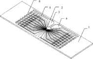
图1为本发明离体神经信息双模检测微电极阵列芯片结构图;Fig. 1 is a structural diagram of a microelectrode array chip for dual-mode detection of isolated nerve information of the present invention;
图2为两种不同微电极阵列的局部放大示意图,其中:Figure 2 is a partially enlarged schematic diagram of two different microelectrode arrays, wherein:
图2a中的微电极直径均为30μm;The diameters of the microelectrodes in Figure 2a are all 30 μm;
图2b中的微电极直径包含10μm、20μm、30μm、40μm、50μm五种;The microelectrode diameters in Figure 2b include five types: 10 μm, 20 μm, 30 μm, 40 μm, and 50 μm;
图3为本发明离体神经信息双模检测微电极阵列芯片制备方法的工艺流程图;Fig. 3 is a process flow chart of the preparation method of the microelectrode array chip for dual-mode detection of isolated nerve information of the present invention;
图3a为电极引线及触点的图案;Figure 3a is the pattern of electrode leads and contacts;
图3b为接着溅射250nm的Pt薄膜层;Fig. 3 b is the Pt film layer of sputtering 250nm next;
图3c为采用剥离工艺去除多余的Ti/Pt薄膜层,留下所需电极、引线及触点;Figure 3c shows that the redundant Ti/Pt film layer is removed by stripping process, leaving the required electrodes, leads and contacts;
图3d为在制备好Pt薄膜层的基底表面,PECVD氮化硅(Si3N4)绝缘层,厚度800nm。通过光刻和SF6等离子刻蚀的方法,暴露出微电极、对电极、参比电极及触点,保留所有引线表面覆盖的氮化硅绝缘层;FIG. 3 d shows a PECVD silicon nitride (Si3 N4 ) insulating layer with a thickness of 800 nm on the surface of the prepared Pt thin film substrate. Through photolithography and SF6 plasma etching, the micro-electrodes, counter electrodes, reference electrodes and contacts are exposed, and the silicon nitride insulating layer covered on the surface of all leads is retained;
图3e为在参比电极的表面,丝印涂覆厚度200μm的Ag/AgCl浆料,并在100℃的烘箱中烘干3小时,最终形成Ag/AgCl复合薄膜参比电极;Figure 3e is the Ag/AgCl slurry coated with a thickness of 200 μm by screen printing on the surface of the reference electrode, and dried in an oven at 100°C for 3 hours to finally form a Ag/AgCl composite thin film reference electrode;
图3f为采用电化学沉积的方法,在用于神经电生理检测的微电极表面修饰纳米铂黑(Pt Black)颗粒;Fig. 3 f is the method for adopting electrochemical deposition to modify nano-platinum black (Pt Black) particles on the surface of a microelectrode for neuroelectrophysiological detection;
图3g为在微电极阵列表面滴涂浓度为1%的Nafion(离子交换型聚合物)乙醇溶液,自然晾干后,形成离子选择性Nafion薄膜。Fig. 3g shows that a Nafion (ion-exchange polymer) ethanol solution with a concentration of 1% is drip-coated on the surface of the microelectrode array, and after natural drying, an ion-selective Nafion film is formed.
附图标号说明:1为绝缘基底,2为微电极阵列,3为对电极,4为参比电极,5为引线,6为触点,7为可功能复用的微电极,8为仅用于电生理检测的微电极,9为仅用于神经递质检测或施加电刺激的微电极。Explanation of reference numerals: 1 is an insulating substrate, 2 is a microelectrode array, 3 is a counter electrode, 4 is a reference electrode, 5 is a lead wire, 6 is a contact, 7 is a microelectrode that can be reused, 8 is a microelectrode that can only be used Microelectrode used for electrophysiological detection, 9 is a microelectrode only used for neurotransmitter detection or application of electrical stimulation.
具体实施方式Detailed ways
本发明离体神经信息双模检测微电极阵列芯片,由绝缘基底、微电极阵列、对电极、参比电极、电极引线以及触点构成。所述绝缘基底是整个芯片的载体,在绝缘基底表面的中心位置,分布了若干个以矩阵形式排布的、由导电薄膜材料制成的圆形微电极,构成微电极阵列。其中,部分微电极用于检测神经电生理信号,部分微电极用于检测不同神经递质的浓度或对神经细胞施加电刺激。微电极阵列周边配有一个尺寸较大的Pt薄膜对电极,以及一个Ag/AgCl复合薄膜参比电极。所有圆形微电极均通过导电薄膜引线延伸至基底边缘,末端形成方形触点,方便与外部电路连接,所有引线表面均覆盖有绝缘层。The micro-electrode array chip for dual-mode detection of isolated nerve information of the present invention is composed of an insulating substrate, a micro-electrode array, a counter electrode, a reference electrode, electrode leads and contacts. The insulating base is the carrier of the whole chip. Several circular micro-electrodes arranged in matrix and made of conductive film materials are distributed in the center of the surface of the insulating base to form a micro-electrode array. Among them, some microelectrodes are used to detect neurophysiological signals, and some microelectrodes are used to detect the concentration of different neurotransmitters or apply electrical stimulation to nerve cells. A larger Pt thin film counter electrode and an Ag/AgCl composite thin film reference electrode are arranged around the microelectrode array. All circular microelectrodes are extended to the edge of the substrate through conductive film leads, and the ends form square contacts for easy connection with external circuits, and the surfaces of all leads are covered with insulating layers.
绝缘基底选用硬质透明绝缘材料,可以是石英玻璃、聚氯乙烯、聚碳酸酯,这些材料具有化学、机械性能稳定的特点,能够耐受微加工过程中温度、压力、化学试剂的影响。选用透明材料有利于在显微镜下对被测离体神经细胞进行观察。绝缘基底边长25mm~80mm,厚度1mm~2mm。The insulating base is made of hard and transparent insulating materials, such as quartz glass, polyvinyl chloride, and polycarbonate. These materials have stable chemical and mechanical properties and can withstand the influence of temperature, pressure, and chemical reagents during micro-processing. The selection of transparent materials is beneficial to observe the isolated nerve cells under the microscope. The side length of the insulating base is 25mm-80mm, and the thickness is 1mm-2mm.
微电极阵列选用的导电薄膜材料为生物相容性好的金属或金属化合物,可以是金、铂、氮化钛、铟锡氧化物,为了提高信噪比以及提高对不同神经递质检测的选择性,微电极表面可根据需要修饰纳米材料或敏感膜材料。The conductive film material selected for the microelectrode array is a metal or metal compound with good biocompatibility, which can be gold, platinum, titanium nitride, indium tin oxide, in order to improve the signal-to-noise ratio and improve the selection of different neurotransmitter detection The surface of the microelectrode can be modified with nanomaterials or sensitive membrane materials as needed.
微电极阵列包含9~64个微电极,其中用于神经电生理信号检测的微电极直径10μm~30μm,用于神经递质电化学信号检测以及施加电刺激的微电极直径30μm~50μm,微电极间距50μm~200μm。The microelectrode array contains 9 to 64 microelectrodes, of which the diameter of the microelectrode used for the detection of neurophysiological signals is 10 μm to 30 μm, and the diameter of the microelectrode used for the detection of neurotransmitter electrochemical signals and the application of electrical stimulation is 30 μm to 50 μm. The pitch is 50 μm to 200 μm.
对电极及参比电极的尺寸比微电极至少大一个数量级,在电生理信号检测或施加电刺激的过程中,参比电极用于提供参考电位;在神经递质电化学信号的检测过程中,对电极用于提供一个电流回路,并与参比电极一起,构成电化学检测的三电极体系。The size of the counter electrode and the reference electrode is at least an order of magnitude larger than that of the microelectrode. During the detection of electrophysiological signals or the application of electrical stimulation, the reference electrode is used to provide a reference potential; during the detection of neurotransmitter electrochemical signals, The counter electrode is used to provide a current loop, and together with the reference electrode, constitutes a three-electrode system for electrochemical detection.
圆形微电极引线及触点的导电薄膜材料与微电极相同,厚度大于300nm,保证其机械强度能够承受标准电子元器件中弹性金属探针所造成的压力。当金属探针轻压在触点上时,即可实现芯片与外部电路的连接。该电路接口避免了常规MEMS器件封装时金丝压焊的工序,接口简单,连接可靠,可重复使用。The conductive film material of the circular microelectrode leads and contacts is the same as that of the microelectrode, and the thickness is greater than 300nm, which ensures that its mechanical strength can withstand the pressure caused by the elastic metal probe in standard electronic components. When the metal probe is lightly pressed on the contact, the connection between the chip and the external circuit can be realized. The circuit interface avoids the process of gold wire pressure welding during conventional MEMS device packaging, has simple interface, reliable connection and can be used repeatedly.
圆形微电极引线表面覆盖的绝缘层材料为生物相容性好的有机或无机绝缘材料,可以是二氧化硅、氮化硅、氮氧硅、SU8、聚酰亚胺、聚对二甲苯。The material of the insulating layer covered on the surface of the circular microelectrode lead is an organic or inorganic insulating material with good biocompatibility, such as silicon dioxide, silicon nitride, silicon oxynitride, SU8, polyimide, and parylene.
本发明的离体神经信息双模检测微电极阵列芯片,其制备方法包括如下步骤:The preparation method of the isolated nerve information dual-mode detection microelectrode array chip of the present invention comprises the following steps:
1.在经过表面清洗的绝缘基底上旋涂一层光刻胶,厚度大于拟溅射导电薄膜层的三倍,光刻显影后形成所有微电极阵列、对电极、参比电极、电极引线及触点的图案;1. Spin-coat a layer of photoresist on the surface-cleaned insulating substrate, the thickness of which is three times greater than that of the conductive film layer to be sputtered. After photolithography and development, all micro-electrode arrays, counter electrodes, reference electrodes, electrode leads and the pattern of the contacts;
2.在光刻胶图案表面溅射一层厚度250nm~500nm的微电极导电薄膜层,必要时预先溅射10nm~50nm的Cr或Ti种子层,以增加导电薄膜层与基底的粘附性;2. Sputter a microelectrode conductive film layer with a thickness of 250nm to 500nm on the surface of the photoresist pattern, and pre-sputter a 10nm to 50nm Cr or Ti seed layer if necessary to increase the adhesion between the conductive film layer and the substrate;
3.采用剥离工艺去除多余导电薄膜层,留下所需电极、引线及触点;3. Use the stripping process to remove the excess conductive film layer, leaving the required electrodes, leads and contacts;
4.通过PECVD二氧化硅、氮化硅、氮氧硅,或旋涂SU8、聚酰亚胺、聚对二甲苯的方法,在制备好导电薄膜层的基底表面覆盖绝缘层,通过光刻和等离子刻蚀的方法,暴露出微电极、对电极、参比电极及触点,保留所有引线表面覆盖的绝缘层;4. By PECVD silicon dioxide, silicon nitride, silicon oxynitride, or spin-coating SU8, polyimide, parylene, cover the insulating layer on the substrate surface of the prepared conductive film layer, through photolithography and The method of plasma etching exposes the micro-electrodes, counter electrodes, reference electrodes and contacts, and retains the insulating layer covered on the surface of all leads;
5.在所述对电极的表面,采用光刻、溅射、剥离的工艺,制备厚度250nm~500nm的Pt金属薄膜层,若步骤2中的微电极导电薄膜已选用Pt,则可省略本步骤;5. On the surface of the counter electrode, a Pt metal film layer with a thickness of 250nm to 500nm is prepared by photolithography, sputtering, and stripping. If the microelectrode conductive film in
6.在所述参比电极的表面,采用光刻、溅射、剥离的工艺,制备厚度500nm~800nm的Ag金属薄膜层,并通过化学或电化学方法进行氯化,或在参比电极的表面丝印涂覆Ag/AgCl浆料并烘干,最终形成Ag/AgCl复合薄膜参比电极;6. On the surface of the reference electrode, adopt photolithography, sputtering, and stripping processes to prepare an Ag metal thin film layer with a thickness of 500nm to 800nm, and chlorinate it by chemical or electrochemical methods, or on the surface of the reference electrode Coat the Ag/AgCl slurry on the surface with silk screen printing and dry it to form a Ag/AgCl composite film reference electrode;
7.通过电化学沉积或物理滴涂、吸附的方法,在设定不同功能的微电极表面修饰纳米材料或敏感膜材料。7. Modify nanomaterials or sensitive membrane materials on the surface of microelectrodes with different functions by means of electrochemical deposition or physical drop coating and adsorption.
以下结合附图对本发明的一个具体实施方式做详细说明。A specific embodiment of the present invention will be described in detail below in conjunction with the accompanying drawings.
本发明提供的离体神经信息双模检测微电极阵列芯片结构如图1所示。整个芯片由绝缘基底1、微电极阵列2、对电极3、参比电极4、电极引线5以及触点6构成。The structure of the isolated nerve information dual-mode detection microelectrode array chip provided by the present invention is shown in FIG. 1 . The whole chip is composed of an insulating substrate 1 , a
绝缘基底1选用生物实验室常用的载玻片,作为整个芯片的载体。载玻片长76.2mm,宽25.4mm,厚1mm。在载玻片表面的中心位置,分布了64个由Pt薄膜材料制成的圆形微电极,构成微电极阵列2。The insulating substrate 1 is a glass slide commonly used in biological laboratories as a carrier for the entire chip. The slide glass is 76.2mm long, 25.4mm wide, and 1mm thick. At the center of the surface of the glass slide, 64 circular microelectrodes made of Pt thin film material are distributed to form a
微电极基本以8×8的方阵形式排列,电极间距100μm,亦可做一定形式的调整。图2即为两种不同微电极阵列2的局部放大示意图,图2(a)中的微电极直径均为30μm,图2(b)中的微电极直径包含10μm、20μm、30μm、40μm、50μm五种。由于待测神经细胞的胞体直径在10μm左右,电极直径越小越利于检测单个细胞的电活动,电极直径大于30μm时,电极记录到的信号过多,将不利于单个细胞电信号的分离。但是,大的电极直径有利于增加神经递质检测的信号强度,且能够承受更大的刺激电流。因此,本实施例中,直径小于30μm的微电极仅用于检测神经细胞的电生理信号,如图中的电极7;直径大于30μm的微电极仅用于检测神经递质电化学信号,或对神经细胞进行电刺激,如图中的电极9;直径为30μm的微电极则可根据需要进行三种功能的切换,如图中的电极8。为了提高信噪比,可在微电极表面修饰纳米铂黑颗粒。为了提高检测神经递质多巴胺的选择性,可在微电极表面修饰离子选择性Nafion膜。The microelectrodes are basically arranged in a square matrix of 8×8, with an electrode spacing of 100 μm, and can also be adjusted in a certain form. Figure 2 is a partially enlarged schematic diagram of two
在载玻片的一侧配有一个尺寸较大的Pt薄膜对电极3,以及一个Ag/AgCl复合薄膜参比电极4。两个电极均呈多边形,对称分布,尾端呈条形分别延伸至载玻片边缘,最小边长约3mm左右。在电生理信号检测或施加电刺激的过程中,参比电极用于提供参考电位;在神经递质电化学信号的检测过程中,对电极3用于提供一个电流回路,并与参比电极一起,构成电化学检测的三电极体系。One side of the glass slide is provided with a relatively large Pt thin
所有圆形微电极均通过Pt薄膜引线5延伸至载玻片两端边缘,末端形成方形触点6,触点边长1.27mm,同样以阵列形式排布,间距2.54mm。该尺寸与标准电子元器件中弹性金属探针的尺寸相匹配。当焊接在电路板上的金属探针轻压在触点上时,即可实现芯片与外部电路的连接。All circular microelectrodes are extended to the edges of both ends of the glass slide through Pt film leads 5, and the ends form
所有引线表面均覆盖有氮化硅薄膜绝缘层,可使神经细胞及电解质培养液与引线之间达到电学上的隔离。将离体的动物神经组织切片贴在芯片的微电极阵列表面,或在芯片上进行神经细胞培养,结合配套的检测系统,即可开展动物离体神经信息的双模检测及相关研究。The surfaces of all lead wires are covered with a silicon nitride film insulating layer, which can achieve electrical isolation between the nerve cells and electrolyte culture solution and the lead wires. Paste isolated animal nerve tissue slices on the surface of the microelectrode array of the chip, or culture nerve cells on the chip, and combine with the supporting detection system to carry out dual-mode detection and related research of animal nerve information in vitro.
本发明的具体制备过程参考图3详述如下:Concrete preparation process of the present invention is described in detail as follows with reference to Fig. 3:
1.在经过表面清洗的载玻片(Glass)上旋涂一层正性光刻胶AZ1500,厚度1μm,光刻显影后形成掩模板上所有微电极阵列2、对电极3、参比电极4、电极引线及触点6的图案(图3a);1. Spin-coat a layer of positive photoresist AZ1500 on the surface-cleaned glass (Glass), with a thickness of 1 μm, and form all microelectrode arrays on the mask after photolithography and
2.在光刻胶图案表面溅射一层厚度30nm的Ti种子层,以增加Pt导电薄膜层与玻璃基底的粘附性,接着溅射250nm的Pt薄膜层(图3b)。2. Sputter a Ti seed layer with a thickness of 30nm on the surface of the photoresist pattern to increase the adhesion between the Pt conductive film layer and the glass substrate, and then sputter a 250nm Pt film layer (Figure 3b).
3.采用剥离工艺去除多余的Ti/Pt薄膜层,留下所需电极2~4、引线5及触点6,(图3c);3. Remove the redundant Ti/Pt film layer by stripping process, leaving the required electrodes 2-4, leads 5 and
4.在制备好Pt薄膜层的基底表面,PECVD氮化硅(Si3N4)绝缘层,厚度800nm。通过光刻和SF6等离子刻蚀的方法,暴露出微电极7、8、对电极3、参比电极4及触点6,保留所有引线表面覆盖的氮化硅绝缘层(图3d);4. PECVD a silicon nitride (Si3 N4 ) insulating layer with a thickness of 800 nm on the surface of the prepared Pt thin film substrate. By means of photolithography andSF6 plasma etching, the
5.在参比电极4的表面,丝印涂覆厚度200μm的Ag/AgCl浆料,并在100℃的烘箱中烘干3小时,最终形成Ag/AgCl复合薄膜参比电极4(图3e);5. On the surface of the
7.采用电化学沉积的方法,在用于神经电生理检测的微电极8表面修饰纳米铂黑(Pt Black)颗粒(图3f)。具体过程是,用去离子水配制20mmol/L的氯铂酸(H2PtCl6)和2mol/L的盐酸(HCl)混合液,作为电镀液加入灌流槽中。连接电化学工作站CHI660,以待修饰微电极为工作电极,铂丝为对电极,施加固定电位,采用计时电流法电镀5分钟。7. Using the electrochemical deposition method, the surface of the
8.在微电极阵列2表面滴涂浓度为1%的Nafion(离子交换型聚合物)乙醇溶液,自然晾干后,形成离子选择性Nafion薄膜(图3g)。8. A Nafion (ion-exchange polymer) ethanol solution with a concentration of 1% was drip-coated on the surface of the
以上实施例只是为了起到说明的目的,并非对本发明的限制,在上述说明的基础上,可以对本发明作许多改进和改变,所作改进和改变,及选用其它功能材料等方法均应在本发明权利要求保护范围之内。Above embodiment is only for the purpose of playing description, not limitation of the present invention, on the basis of above description, can make many improvements and changes to the present invention, the improvements and changes made, and methods such as selecting other functional materials all should be included in the present invention. within the scope of the claims.
Claims (8)
Priority Applications (1)
| Application Number | Priority Date | Filing Date | Title |
|---|---|---|---|
| CN201010513818.5ACN102445477B (en) | 2010-10-13 | 2010-10-13 | Microelectrode array chip for dual-mode detection of isolated nerve information and its preparation method |
Applications Claiming Priority (1)
| Application Number | Priority Date | Filing Date | Title |
|---|---|---|---|
| CN201010513818.5ACN102445477B (en) | 2010-10-13 | 2010-10-13 | Microelectrode array chip for dual-mode detection of isolated nerve information and its preparation method |
Publications (2)
| Publication Number | Publication Date |
|---|---|
| CN102445477Atrue CN102445477A (en) | 2012-05-09 |
| CN102445477B CN102445477B (en) | 2014-02-12 |
Family
ID=46008181
Family Applications (1)
| Application Number | Title | Priority Date | Filing Date |
|---|---|---|---|
| CN201010513818.5AActiveCN102445477B (en) | 2010-10-13 | 2010-10-13 | Microelectrode array chip for dual-mode detection of isolated nerve information and its preparation method |
Country Status (1)
| Country | Link |
|---|---|
| CN (1) | CN102445477B (en) |
Cited By (29)
| Publication number | Priority date | Publication date | Assignee | Title |
|---|---|---|---|---|
| CN102749372A (en)* | 2012-06-06 | 2012-10-24 | 张治红 | SnO2 based electrochemical biological chip and preparation method and application |
| CN103031246A (en)* | 2011-10-10 | 2013-04-10 | 中国科学院电子学研究所 | Microelectrode array chip for multi-parameter detection of nerve cells and preparation method thereof |
| CN103035774A (en)* | 2012-12-31 | 2013-04-10 | 东南大学 | Single-light-source implantable nerve multipoint synchronous interaction chip and preparation method thereof |
| CN103630571A (en)* | 2013-09-12 | 2014-03-12 | 中国科学院电子学研究所 | Micro-nano array sensor and preparation method thereof |
| CN103630583A (en)* | 2013-04-27 | 2014-03-12 | 中国科学院电子学研究所 | Multizone multifunctional nerve dual-mode detection microelectrode array chip and preparation method |
| CN103627631A (en)* | 2013-04-27 | 2014-03-12 | 中国科学院电子学研究所 | Polypyrrole/graphene decorated dual-mode nerve microelectrode array chip and preparation method thereof |
| CN103675048A (en)* | 2013-11-18 | 2014-03-26 | 西安交通大学 | Metal-oxide gas sensor based on MEMS (Micro-Electro-Mechanic System) and preparation technology thereof |
| CN103663342A (en)* | 2013-11-15 | 2014-03-26 | 上海交通大学 | Common wiring microelectrode array chip and manufacturing method thereof |
| CN104760922A (en)* | 2014-01-03 | 2015-07-08 | 中国科学院电子学研究所 | Ultramicro planar electrode array sensor and preparation method thereof |
| CN105116017A (en)* | 2015-09-08 | 2015-12-02 | 无锡百灵传感技术有限公司 | Chip type integrated sensor |
| CN105137023A (en)* | 2015-10-14 | 2015-12-09 | 无锡百灵传感技术有限公司 | System and method for detecting aquatic products online |
| CN105403593A (en)* | 2015-11-27 | 2016-03-16 | 北京大学深圳研究院 | Method for detecting neurotoxicity of magnesium or magnesium alloy |
| CN106124596A (en)* | 2016-06-30 | 2016-11-16 | 英太格电子科技(苏州)有限公司 | A kind of preparation technology of biochemical test sheet |
| CN108254414A (en)* | 2018-03-09 | 2018-07-06 | 国家纳米科学中心 | A kind of flexible in vitro micro- raceway groove microelectrode array integrated chip and its preparation method and application |
| CN108294741A (en)* | 2017-01-12 | 2018-07-20 | 国家纳米科学中心 | A kind of miniature flexible biologic electrode array and preparation method thereof |
| CN109211992A (en)* | 2017-06-29 | 2019-01-15 | 深圳市理邦精密仪器股份有限公司 | Electrode circuit board for biochemical measurement of blood gas and method for manufacturing electrode |
| CN110108905A (en)* | 2019-05-22 | 2019-08-09 | 长春理工大学 | A kind of nervous cell membrane potential and neuron membrane repair behavioral value method and device |
| WO2019169789A1 (en)* | 2018-03-09 | 2019-09-12 | 深圳市刷新智能电子有限公司 | Sweat sensor and preparation method therefor |
| CN110935495A (en)* | 2019-11-29 | 2020-03-31 | 中国科学院电子学研究所 | GABA and electrophysiological micro-nano synchronous sensing detection chip and preparation method thereof |
| CN111398898A (en)* | 2020-04-08 | 2020-07-10 | 中国科学院长春光学精密机械与物理研究所 | Neural mimicry bionic curved surface compound eye system for large-field-of-view three-dimensional motion detection |
| CN111956218A (en)* | 2020-08-10 | 2020-11-20 | 中国科学院上海微系统与信息技术研究所 | Flexible brain electrode with electrochemical and electrophysiological detection functions and preparation method thereof |
| CN111973173A (en)* | 2020-08-31 | 2020-11-24 | 中国科学院空天信息创新研究院 | Microelectrode array chip for hippocampal brain slices, modification method and test method |
| CN112221012A (en)* | 2020-10-19 | 2021-01-15 | 厦门展虹创健科技有限公司 | Electromyographic signal collector and rehabilitation system |
| CN113683051A (en)* | 2021-07-26 | 2021-11-23 | 长春理工大学 | Large-area electronic circuit manufacturing technology based on DEP assembly principle |
| CN113684133A (en)* | 2021-09-09 | 2021-11-23 | 中国科学院空天信息创新研究院 | Neuron NOT-gate logic function chip integrating micro-fluidic and microelectrode array and preparation method thereof |
| CN114634152A (en)* | 2022-02-28 | 2022-06-17 | 复旦大学 | Neural electrode array with cross-size electrode points and design method thereof |
| CN115211995A (en)* | 2022-07-18 | 2022-10-21 | 天津大学 | Flexible intelligent sensing tooth socket |
| CN115266871A (en)* | 2021-04-30 | 2022-11-01 | 苏州科技大学 | Real-time free radical biomedical detection chip device and application thereof |
| CN115886827A (en)* | 2022-11-28 | 2023-04-04 | 中国科学技术大学 | Neural microelectrode with temperature regulation and temperature measurement functions and preparation method thereof |
Citations (2)
| Publication number | Priority date | Publication date | Assignee | Title |
|---|---|---|---|---|
| CN1131744A (en)* | 1994-06-13 | 1996-09-25 | 松下电器产业株式会社 | Cell Potential Measurement Device |
| CN1427255A (en)* | 2001-12-17 | 2003-07-02 | 清华大学 | Apparatus for irritating animal cell and recording its physiological signal and its production and using method |
- 2010
- 2010-10-13CNCN201010513818.5Apatent/CN102445477B/enactiveActive
Patent Citations (2)
| Publication number | Priority date | Publication date | Assignee | Title |
|---|---|---|---|---|
| CN1131744A (en)* | 1994-06-13 | 1996-09-25 | 松下电器产业株式会社 | Cell Potential Measurement Device |
| CN1427255A (en)* | 2001-12-17 | 2003-07-02 | 清华大学 | Apparatus for irritating animal cell and recording its physiological signal and its production and using method |
Non-Patent Citations (2)
| Title |
|---|
| 《Sensor and Actuators》 20011231 Timothy D. Strong et al "A microelectrode array for real-time neurochemical and neuroelectrical recording in vitro" 第357-362页 1、2 第91卷,* |
| TIMOTHY D. STRONG ET AL: ""A microelectrode array for real-time neurochemical and neuroelectrical recording in vitro"", 《SENSOR AND ACTUATORS》* |
Cited By (42)
| Publication number | Priority date | Publication date | Assignee | Title |
|---|---|---|---|---|
| CN103031246A (en)* | 2011-10-10 | 2013-04-10 | 中国科学院电子学研究所 | Microelectrode array chip for multi-parameter detection of nerve cells and preparation method thereof |
| CN103031246B (en)* | 2011-10-10 | 2014-11-05 | 中国科学院电子学研究所 | Microelectrode array chip for multi-parameter detection of nerve cells and preparation method thereof |
| CN102749372B (en)* | 2012-06-06 | 2014-05-14 | 张治红 | SnO2 based electrochemical biological chip and preparation method and application |
| CN102749372A (en)* | 2012-06-06 | 2012-10-24 | 张治红 | SnO2 based electrochemical biological chip and preparation method and application |
| CN103035774A (en)* | 2012-12-31 | 2013-04-10 | 东南大学 | Single-light-source implantable nerve multipoint synchronous interaction chip and preparation method thereof |
| CN103035774B (en)* | 2012-12-31 | 2015-07-01 | 东南大学 | Single-light-source implantable nerve multipoint synchronous interaction chip and preparation method thereof |
| CN103627631A (en)* | 2013-04-27 | 2014-03-12 | 中国科学院电子学研究所 | Polypyrrole/graphene decorated dual-mode nerve microelectrode array chip and preparation method thereof |
| CN103630583A (en)* | 2013-04-27 | 2014-03-12 | 中国科学院电子学研究所 | Multizone multifunctional nerve dual-mode detection microelectrode array chip and preparation method |
| CN103630571A (en)* | 2013-09-12 | 2014-03-12 | 中国科学院电子学研究所 | Micro-nano array sensor and preparation method thereof |
| CN103630571B (en)* | 2013-09-12 | 2015-08-19 | 中国科学院电子学研究所 | A kind of micro-nano array sensor and preparation method thereof |
| CN103663342B (en)* | 2013-11-15 | 2016-03-02 | 上海交通大学 | Connect up microelectrode array chip and preparation method thereof altogether |
| CN103663342A (en)* | 2013-11-15 | 2014-03-26 | 上海交通大学 | Common wiring microelectrode array chip and manufacturing method thereof |
| CN103675048B (en)* | 2013-11-18 | 2016-02-24 | 西安交通大学 | A kind of metal-oxide gas transducer based on MEMS and preparation technology |
| CN103675048A (en)* | 2013-11-18 | 2014-03-26 | 西安交通大学 | Metal-oxide gas sensor based on MEMS (Micro-Electro-Mechanic System) and preparation technology thereof |
| CN104760922A (en)* | 2014-01-03 | 2015-07-08 | 中国科学院电子学研究所 | Ultramicro planar electrode array sensor and preparation method thereof |
| CN104760922B (en)* | 2014-01-03 | 2016-08-24 | 中国科学院电子学研究所 | A kind of ultra micro planar electrode array sensor and preparation method thereof |
| CN105116017A (en)* | 2015-09-08 | 2015-12-02 | 无锡百灵传感技术有限公司 | Chip type integrated sensor |
| CN105137023A (en)* | 2015-10-14 | 2015-12-09 | 无锡百灵传感技术有限公司 | System and method for detecting aquatic products online |
| CN105403593A (en)* | 2015-11-27 | 2016-03-16 | 北京大学深圳研究院 | Method for detecting neurotoxicity of magnesium or magnesium alloy |
| CN106124596A (en)* | 2016-06-30 | 2016-11-16 | 英太格电子科技(苏州)有限公司 | A kind of preparation technology of biochemical test sheet |
| CN108294741A (en)* | 2017-01-12 | 2018-07-20 | 国家纳米科学中心 | A kind of miniature flexible biologic electrode array and preparation method thereof |
| CN109211992A (en)* | 2017-06-29 | 2019-01-15 | 深圳市理邦精密仪器股份有限公司 | Electrode circuit board for biochemical measurement of blood gas and method for manufacturing electrode |
| CN108254414A (en)* | 2018-03-09 | 2018-07-06 | 国家纳米科学中心 | A kind of flexible in vitro micro- raceway groove microelectrode array integrated chip and its preparation method and application |
| WO2019169789A1 (en)* | 2018-03-09 | 2019-09-12 | 深圳市刷新智能电子有限公司 | Sweat sensor and preparation method therefor |
| CN108254414B (en)* | 2018-03-09 | 2024-02-02 | 国家纳米科学中心 | Flexible in-vitro micro-channel microelectrode array integrated chip and preparation method and application thereof |
| CN110108905A (en)* | 2019-05-22 | 2019-08-09 | 长春理工大学 | A kind of nervous cell membrane potential and neuron membrane repair behavioral value method and device |
| CN110108905B (en)* | 2019-05-22 | 2021-08-06 | 长春理工大学 | A kind of nerve cell membrane potential and nerve cell membrane repair behavior detection method and device |
| CN110935495B (en)* | 2019-11-29 | 2021-02-23 | 中国科学院电子学研究所 | GABA and electrophysiological micro-nano synchronous sensing detection chip and preparation method thereof |
| CN110935495A (en)* | 2019-11-29 | 2020-03-31 | 中国科学院电子学研究所 | GABA and electrophysiological micro-nano synchronous sensing detection chip and preparation method thereof |
| CN111398898A (en)* | 2020-04-08 | 2020-07-10 | 中国科学院长春光学精密机械与物理研究所 | Neural mimicry bionic curved surface compound eye system for large-field-of-view three-dimensional motion detection |
| CN111956218A (en)* | 2020-08-10 | 2020-11-20 | 中国科学院上海微系统与信息技术研究所 | Flexible brain electrode with electrochemical and electrophysiological detection functions and preparation method thereof |
| CN111956218B (en)* | 2020-08-10 | 2024-04-16 | 中国科学院上海微系统与信息技术研究所 | Flexible brain electrode with electrochemical and electrophysiological detection functions and preparation method thereof |
| CN111973173B (en)* | 2020-08-31 | 2023-04-07 | 中国科学院空天信息创新研究院 | Microelectrode array chip for hippocampal brain slices, modification method and test method |
| CN111973173A (en)* | 2020-08-31 | 2020-11-24 | 中国科学院空天信息创新研究院 | Microelectrode array chip for hippocampal brain slices, modification method and test method |
| CN112221012A (en)* | 2020-10-19 | 2021-01-15 | 厦门展虹创健科技有限公司 | Electromyographic signal collector and rehabilitation system |
| CN115266871A (en)* | 2021-04-30 | 2022-11-01 | 苏州科技大学 | Real-time free radical biomedical detection chip device and application thereof |
| CN113683051A (en)* | 2021-07-26 | 2021-11-23 | 长春理工大学 | Large-area electronic circuit manufacturing technology based on DEP assembly principle |
| CN113684133A (en)* | 2021-09-09 | 2021-11-23 | 中国科学院空天信息创新研究院 | Neuron NOT-gate logic function chip integrating micro-fluidic and microelectrode array and preparation method thereof |
| CN113684133B (en)* | 2021-09-09 | 2023-11-24 | 中国科学院空天信息创新研究院 | A neuron NOT gate logic functional chip integrating microfluidics and microelectrode array and its preparation method |
| CN114634152A (en)* | 2022-02-28 | 2022-06-17 | 复旦大学 | Neural electrode array with cross-size electrode points and design method thereof |
| CN115211995A (en)* | 2022-07-18 | 2022-10-21 | 天津大学 | Flexible intelligent sensing tooth socket |
| CN115886827A (en)* | 2022-11-28 | 2023-04-04 | 中国科学技术大学 | Neural microelectrode with temperature regulation and temperature measurement functions and preparation method thereof |
Also Published As
| Publication number | Publication date |
|---|---|
| CN102445477B (en) | 2014-02-12 |
Similar Documents
| Publication | Publication Date | Title |
|---|---|---|
| CN102445477B (en) | Microelectrode array chip for dual-mode detection of isolated nerve information and its preparation method | |
| CN102783942B (en) | Implantable neural information dual-mode detection microelectrode array chip and manufacturing method thereof | |
| CN103031246B (en) | Microelectrode array chip for multi-parameter detection of nerve cells and preparation method thereof | |
| US20220175278A1 (en) | Solid-state substrate-integrated reference electrode and counter electrode | |
| CN103630583A (en) | Multizone multifunctional nerve dual-mode detection microelectrode array chip and preparation method | |
| CN101614729B (en) | Microelectrode array device and special device for cell manipulation and electrophysiological signal detection | |
| CN104760922B (en) | A kind of ultra micro planar electrode array sensor and preparation method thereof | |
| CN103627631A (en) | Polypyrrole/graphene decorated dual-mode nerve microelectrode array chip and preparation method thereof | |
| CN1190665C (en) | Multi-electrode for determining electrophysiological characteristics of biological specimens, multi-electrode integrated cell support, cell potential measuring device and cell potential measuring system | |
| CN103829938B (en) | Microelectrode array implanted chip and preparation method thereof | |
| CN111982988B (en) | Microelectrode array chip for detecting dopamine release and preparation method thereof | |
| CN106725470B (en) | A continuous or discontinuous physiological parameter analysis system | |
| CN107957440B (en) | Planar ammonia selective sensing electrode and method for making the same | |
| US20190380635A1 (en) | Dual-Sided Biomorphic Polymer-based Microelectrode Array and Fabrication Thereof | |
| JP3193471B2 (en) | Integrated composite electrode | |
| JP3101122B2 (en) | Integrated composite electrode | |
| CN107462511A (en) | Pass through the device of nano-electrode An arrayed recording endocellular electricity signal | |
| CN106645346A (en) | Multi-site detection region, microelectrode array and preparation method thereof | |
| US20250027928A1 (en) | Optically transparent microelectrode arrays for electrochemical and electrophysiological measurements or stimulation | |
| CN207882196U (en) | A kind of flexible in vitro micro- raceway groove microelectrode array integrated chip | |
| JP2003287513A (en) | Array electrode for biological sample and method for producing the same | |
| CN111973173B (en) | Microelectrode array chip for hippocampal brain slices, modification method and test method | |
| CN110207737B (en) | Microstrip antenna sensor system with linear array structure, sensor, detection method and preparation method | |
| CN108254414B (en) | Flexible in-vitro micro-channel microelectrode array integrated chip and preparation method and application thereof | |
| CN114544721A (en) | Flexible micro-nano electrode sensor and preparation method thereof |
Legal Events
| Date | Code | Title | Description |
|---|---|---|---|
| C06 | Publication | ||
| PB01 | Publication | ||
| C10 | Entry into substantive examination | ||
| SE01 | Entry into force of request for substantive examination | ||
| C14 | Grant of patent or utility model | ||
| GR01 | Patent grant |