CN102437196A - Low-temperature polycrystalline silicon thin film transistor and manufacturing method thereof - Google Patents
Low-temperature polycrystalline silicon thin film transistor and manufacturing method thereofDownload PDFInfo
- Publication number
- CN102437196A CN102437196ACN201110419036XACN201110419036ACN102437196ACN 102437196 ACN102437196 ACN 102437196ACN 201110419036X ACN201110419036X ACN 201110419036XACN 201110419036 ACN201110419036 ACN 201110419036ACN 102437196 ACN102437196 ACN 102437196A
- Authority
- CN
- China
- Prior art keywords
- layer
- channel
- film transistor
- thin film
- source
- Prior art date
- Legal status (The legal status is an assumption and is not a legal conclusion. Google has not performed a legal analysis and makes no representation as to the accuracy of the status listed.)
- Granted
Links
Images


Classifications
- H—ELECTRICITY
- H10—SEMICONDUCTOR DEVICES; ELECTRIC SOLID-STATE DEVICES NOT OTHERWISE PROVIDED FOR
- H10D—INORGANIC ELECTRIC SEMICONDUCTOR DEVICES
- H10D30/00—Field-effect transistors [FET]
- H10D30/60—Insulated-gate field-effect transistors [IGFET]
- H10D30/67—Thin-film transistors [TFT]
- H10D30/6729—Thin-film transistors [TFT] characterised by the electrodes
- H10D30/673—Thin-film transistors [TFT] characterised by the electrodes characterised by the shapes, relative sizes or dispositions of the gate electrodes
- H—ELECTRICITY
- H10—SEMICONDUCTOR DEVICES; ELECTRIC SOLID-STATE DEVICES NOT OTHERWISE PROVIDED FOR
- H10D—INORGANIC ELECTRIC SEMICONDUCTOR DEVICES
- H10D30/00—Field-effect transistors [FET]
- H10D30/60—Insulated-gate field-effect transistors [IGFET]
- H10D30/67—Thin-film transistors [TFT]
- H10D30/674—Thin-film transistors [TFT] characterised by the active materials
- H—ELECTRICITY
- H10—SEMICONDUCTOR DEVICES; ELECTRIC SOLID-STATE DEVICES NOT OTHERWISE PROVIDED FOR
- H10D—INORGANIC ELECTRIC SEMICONDUCTOR DEVICES
- H10D30/00—Field-effect transistors [FET]
- H10D30/60—Insulated-gate field-effect transistors [IGFET]
- H10D30/67—Thin-film transistors [TFT]
- H10D30/6757—Thin-film transistors [TFT] characterised by the structure of the channel, e.g. transverse or longitudinal shape or doping profile
- H—ELECTRICITY
- H10—SEMICONDUCTOR DEVICES; ELECTRIC SOLID-STATE DEVICES NOT OTHERWISE PROVIDED FOR
- H10D—INORGANIC ELECTRIC SEMICONDUCTOR DEVICES
- H10D30/00—Field-effect transistors [FET]
- H10D30/60—Insulated-gate field-effect transistors [IGFET]
- H10D30/67—Thin-film transistors [TFT]
- H10D30/6729—Thin-film transistors [TFT] characterised by the electrodes
- H10D30/673—Thin-film transistors [TFT] characterised by the electrodes characterised by the shapes, relative sizes or dispositions of the gate electrodes
- H10D30/6736—Thin-film transistors [TFT] characterised by the electrodes characterised by the shapes, relative sizes or dispositions of the gate electrodes characterised by the shape of gate insulators
Landscapes
- Thin Film Transistor (AREA)
Abstract
Translated fromChinese
Description
Translated fromChinese技术领域technical field
本发明涉及一种薄膜晶体管及其制造方法,尤其涉及一种低温多晶硅薄膜晶体管及其制造方法。The invention relates to a thin film transistor and a manufacturing method thereof, in particular to a low-temperature polysilicon thin film transistor and a manufacturing method thereof.
背景技术Background technique
有机发光显示器件(OLED )是主动发光器件。相比现在的主流平板显示技术薄膜晶体管液晶显示器(TFT -LCD ),OLED 具有高对比度,广视角,低功耗,体积更薄等优点,有望成为继LCD之后的下一代平板显示技术,是目前平板显示技术中受到关注最多的技术之一。Organic light-emitting display devices (OLEDs) are active light-emitting devices. Compared with the current mainstream flat-panel display technology Thin Film Transistor Liquid Crystal Display (TFT-LCD), OLED has the advantages of high contrast, wide viewing angle, low power consumption, and thinner volume. It is expected to become the next-generation flat-panel display technology after LCD. It is one of the most concerned technologies in flat panel display technology.
目前主要使用低温多晶硅薄膜晶体管(LTPS-TFT)驱动OLED发光,图1是一种现有技术薄膜晶体管的平面图,图2是按照图1中A-A线所形成的截面图。如图1和图2所示,先在玻璃衬底上使用化学气相沉积的方法沉积缓冲层,然后在缓冲层上沉积非晶硅;将非晶硅层使用固相结晶或者准分子激光晶化的方法转化为多晶硅;最后将多晶硅刻蚀成硅岛形状并依次在上面形成绝缘层、栅极金属层、介电层和源漏金属层图案,并最终形成驱动薄膜晶体管。At present, low-temperature polysilicon thin-film transistors (LTPS-TFT) are mainly used to drive OLEDs to emit light. Figure 1 is a plan view of a prior art thin-film transistor, and Figure 2 is a cross-sectional view formed along line A-A in Figure 1 . As shown in Figure 1 and Figure 2, a buffer layer is first deposited on the glass substrate by chemical vapor deposition, and then amorphous silicon is deposited on the buffer layer; the amorphous silicon layer is crystallized by solid phase crystallization or excimer laser The method is converted into polysilicon; finally, the polysilicon is etched into a silicon island shape, and an insulating layer, a gate metal layer, a dielectric layer, and a source-drain metal layer pattern are sequentially formed on it, and finally a driving thin film transistor is formed.
因为驱动OLED发光需要较大的电流,所以驱动TFT需要有较宽的沟道宽度和较短的沟道长度以使宽度和长度的比值足够大,从而驱动TFT能为OLED提供足够的电流以控制和驱动有机电致发光二极管发光。Because driving OLED requires a large current to emit light, the driving TFT needs to have a wider channel width and a shorter channel length to make the ratio of width to length large enough, so that the driving TFT can provide enough current for the OLED to control And drive organic light-emitting diodes to emit light.
为了保证显示屏的分辨率,像素区的面积需要尽可能的小,开口率需要尽可能的大,因此驱动薄膜晶体管以及外围电路不能超过一定的面积,这就决定了薄膜晶体管的沟道宽度不能做的太宽,在这种情况下需要增大薄膜晶体管沟道的宽长比就只能通过减小长度来解决,但是薄膜晶体管沟道长度降低到一定程度会引起漏电流和沟道击穿等现象,造成薄膜晶体管无法工作。In order to ensure the resolution of the display screen, the area of the pixel area needs to be as small as possible, and the aperture ratio needs to be as large as possible, so the driving thin film transistor and peripheral circuits cannot exceed a certain area, which determines that the channel width of the thin film transistor cannot If it is too wide, in this case, it is necessary to increase the width-to-length ratio of the thin film transistor channel, which can only be solved by reducing the length, but reducing the channel length of the thin film transistor to a certain extent will cause leakage current and channel breakdown and other phenomena, causing the thin film transistor to fail to work.
发明内容Contents of the invention
本发明所要解决的技术问题是提供一种低温多晶硅薄膜晶体管及其制造方法,能够有效增大沟道宽度,从而增大薄膜晶体管的宽长比和开口率,且结构简单,易于实施。The technical problem to be solved by the present invention is to provide a low-temperature polysilicon thin film transistor and its manufacturing method, which can effectively increase the channel width, thereby increasing the aspect ratio and aperture ratio of the thin film transistor, and has a simple structure and is easy to implement.
本发明为解决上述技术问题而采用的技术方案是提供一种低温多晶硅薄膜晶体管,包括栅极、源极和漏极,所述源极和漏极之间有沟道隔开,所述栅极和源极、漏极之间形成有多晶硅硅岛图案,其中,所述沟道处的多晶硅硅岛图案上至少有一个凹槽从而形成立体沟道,所述凹槽的深度小于沟道的深度。The technical scheme adopted by the present invention to solve the above-mentioned technical problems is to provide a low-temperature polysilicon thin film transistor, comprising a gate, a source and a drain, the source and the drain are separated by a channel, and the gate A polysilicon island pattern is formed between the source electrode and the drain electrode, wherein there is at least one groove on the polysilicon island pattern at the channel to form a three-dimensional channel, and the depth of the groove is smaller than the depth of the channel .
本发明为解决上述技术问题还提供一种低温多晶硅薄膜晶体管制造方法,如下步骤:首先在玻璃基板上使用化学气相沉积方法依次沉积一层缓冲层和一非晶硅层,采用准分子激光退火或固相结晶方法将非晶硅层晶化为多晶硅层;用第一掩模板,通过光刻在多晶硅层上形成光刻胶图案,所述第一掩模板为多灰阶掩模板,在沟道区域形成第一高度光刻胶层和第二高度光刻胶层,所述第一高度小于第二高度;使用光刻胶图案,通过第一次化学干法刻蚀工序形成包括沟道、源/漏极接触区在内的多晶硅硅岛图案;去除具有第一高度的光刻胶;然后通过第二次化学干法刻蚀工序形成立体沟道图案;在具有硅岛图案的玻璃基板上继续沉积栅极绝缘层和第一金属层,然后经过光刻以及刻蚀工序形成栅极金属图案;在具有栅极金属图案的玻璃基板表面上,再沉积一介电层;接着利用光刻和蚀刻工序在源/漏极接触区上方形成接触孔;最后在玻璃基板表面上沉积第二金属层,接着利用光刻及刻蚀工序,形成源极和漏极。In order to solve the above-mentioned technical problems, the present invention also provides a method for manufacturing a low-temperature polysilicon thin-film transistor. The steps are as follows: firstly, a buffer layer and an amorphous silicon layer are sequentially deposited on a glass substrate by chemical vapor deposition, and an excimer laser annealing or The solid-phase crystallization method crystallizes the amorphous silicon layer into a polysilicon layer; using a first mask to form a photoresist pattern on the polysilicon layer by photolithography, the first mask is a multi-gray scale mask, and the channel A first-height photoresist layer and a second-height photoresist layer are formed in the region, and the first height is smaller than the second height; using the photoresist pattern, the first chemical dry etching process is used to form a channel, a source / polysilicon island pattern within the drain contact region; remove the photoresist with the first height; then form a three-dimensional channel pattern through the second chemical dry etching process; continue on the glass substrate with the silicon island pattern Deposit the gate insulating layer and the first metal layer, and then form the gate metal pattern through photolithography and etching processes; deposit a dielectric layer on the surface of the glass substrate with the gate metal pattern; then use photolithography and etching The process forms a contact hole above the source/drain contact area; finally, deposits a second metal layer on the surface of the glass substrate, and then uses photolithography and etching processes to form the source and drain.
上述的低温多晶硅薄膜晶体管制造方法,其中,所述栅极绝缘层为氧化硅层、氮化硅层或复合绝缘层。In the above method for manufacturing a low-temperature polysilicon thin film transistor, the gate insulating layer is a silicon oxide layer, a silicon nitride layer or a composite insulating layer.
上述的低温多晶硅薄膜晶体管制造方法,其中,所述第一金属层和第二金属层为一铝层、一钨层、一铬层或金属化合物导电层。In the manufacturing method of the above low-temperature polysilicon thin film transistor, wherein, the first metal layer and the second metal layer are an aluminum layer, a tungsten layer, a chromium layer or a metal compound conductive layer.
上述的低温多晶硅薄膜晶体管制造方法,其中,所述介电层为氧化硅或氮化硅。In the above method for manufacturing a low temperature polysilicon thin film transistor, the dielectric layer is silicon oxide or silicon nitride.
本发明对比现有技术有如下的有益效果:本发明提供的低温多晶硅薄膜晶体管及其制造方法,通过衍射曝光在沟道处的多晶硅硅岛图案上形成立体沟道,有效增大沟道宽度,从而增大薄膜晶体管的宽长比和开口率,且结构简单,易于实施。Compared with the prior art, the present invention has the following beneficial effects: the low-temperature polysilicon thin film transistor and its manufacturing method provided by the present invention form a three-dimensional channel on the polysilicon island pattern at the channel by diffraction exposure, effectively increasing the channel width, Therefore, the aspect ratio and aperture ratio of the thin film transistor are increased, and the structure is simple and easy to implement.
附图说明Description of drawings
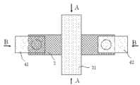
图1为一种低温多晶硅薄膜晶体管平面示意图;1 is a schematic plan view of a low-temperature polysilicon thin film transistor;
图2为现有一种低温多晶硅薄膜晶体管沿A-A线截面图;Fig. 2 is a cross-sectional view along line A-A of an existing low-temperature polysilicon thin film transistor;
图3为本发明低温多晶硅薄膜晶体管沿A-A线截面图;3 is a cross-sectional view along line A-A of a low-temperature polysilicon thin film transistor of the present invention;
图4A为现有低温多晶硅薄膜晶体管沟道宽度示意图;FIG. 4A is a schematic diagram of the channel width of an existing low-temperature polysilicon thin film transistor;
图4B为本发明低温多晶硅薄膜晶体管沟道宽度示意图;FIG. 4B is a schematic diagram of the channel width of the low-temperature polysilicon thin film transistor of the present invention;
图5A为本发明形成缓冲层示意图;FIG. 5A is a schematic diagram of forming a buffer layer in the present invention;
图5B为本发明形成非晶硅层示意图;5B is a schematic diagram of forming an amorphous silicon layer according to the present invention;
图5C为本发明形成多晶硅半导体层示意图;5C is a schematic diagram of forming a polysilicon semiconductor layer according to the present invention;
图5D为本发明多晶硅光刻胶图案形成示意图;5D is a schematic diagram of forming a polysilicon photoresist pattern according to the present invention;
图5E为本发明多晶硅图案形成示意图;FIG. 5E is a schematic diagram of forming a polysilicon pattern according to the present invention;
图5F为本发明灰化工艺后光刻胶形状示意图;5F is a schematic diagram of the shape of the photoresist after the ashing process of the present invention;
图5G为本发明立体沟道形成示意图;Fig. 5G is a schematic diagram of the formation of the three-dimensional channel of the present invention;
图5H为本发明形成栅极绝缘层示意图;FIG. 5H is a schematic diagram of forming a gate insulating layer according to the present invention;
图5I为本发明形成栅极金属层示意图;5I is a schematic diagram of forming a gate metal layer according to the present invention;
图5J为本发明形成栅极图案示意图;FIG. 5J is a schematic diagram of forming a gate pattern according to the present invention;
图5K为本发明形成介电层和源/漏接触孔示意图;FIG. 5K is a schematic diagram of forming a dielectric layer and a source/drain contact hole according to the present invention;
图5L为本发明形成源/漏金属图案示意图。5L is a schematic diagram of forming a source/drain metal pattern according to the present invention.
the
图中:In the picture:
1 缓冲层 2’非晶硅层 2 多晶硅层1 buffer layer 2'amorphous
3 栅绝缘层 4 介电层 5 光刻胶图案3
6 掩膜板 21 凹槽 31 栅极6
41 源极 42 漏极。41
the
具体实施方式Detailed ways
下面结合附图和实施例对本发明作进一步的描述。The present invention will be further described below in conjunction with the accompanying drawings and embodiments.
图3为本发明低温多晶硅薄膜晶体管沿A-A线截面图;图4为本发明与现有一种低温多晶硅薄膜晶体管沟道宽度对比示意图。FIG. 3 is a cross-sectional view along the A-A line of the low-temperature polysilicon thin film transistor of the present invention; FIG. 4 is a schematic diagram of a channel width comparison between the present invention and the existing low-temperature polysilicon thin film transistor.
请参见图3、图4A和图4B,本发明提供的低温多晶硅薄膜晶体管包括栅极31、源极41和漏极42,所述源极41和漏极42之间有沟道隔开,所述栅极31和源极41、漏极42之间形成有多晶硅硅岛图案,其中,所述沟道处的多晶硅硅岛图案上至少有一个凹槽21从而形成立体沟道,所述凹槽21的深度小于沟道的深度。本发明形成的立体薄膜晶体管,沟道宽度增加了立体沟道侧壁的高度(L2+L4),长度L1+L3+L5仍等于现有的长度L;当采用N个凹槽/突起形状时,增加的沟道宽度即为N*(L2+L4),N为自然数,从而明显增大宽长比。凹槽/突起的数目最少为一个,上限由沟道宽度、曝光机分辨率和MASK的制作精度共同决定;凹槽/突起的深度/高度由沟道的深度决定,可以略小于沟道的深度。Referring to FIG. 3, FIG. 4A and FIG. 4B, the low-temperature polysilicon thin film transistor provided by the present invention includes a
下面详细介绍本发明提供的低温多晶硅薄膜晶体管制造方法:The manufacturing method of the low-temperature polysilicon thin film transistor provided by the present invention is introduced in detail below:
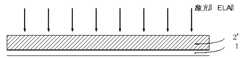
如图5A所示,首先在阵列基板(玻璃)上使用化学气相沉积(CVD)方法沉积一层缓冲层1;如图5B所示,在缓冲层1上使用化学气相沉积(CVD)方法沉积非晶硅层2’;如图5C所示,采用准分子激光退火(ELA)或固相结晶(SPC)方法将非晶硅晶化为多晶硅层2。As shown in Figure 5A, a
如图5D所示,用第一掩模板6,通过光刻在多晶硅层2上形成光刻胶图案5。第一掩模板为多灰阶光掩膜板,可分为Gray-tone mask和Half tone mask两种。 Gray-tone mask是制作出曝光机解析度以下的微缝,再藉由此微缝部位遮住一部份的光源,以达成半曝光的效果。另一方面,Half tone mask是利用「半透过」的膜,来进行半曝光。因为以上两种方式皆是在1次的曝光过程后即可呈现出「曝光部分」「半曝光部分」及「未曝光部分」的3种的曝光层次,故在显影后能够形成2种厚度的光刻胶(感光剂);本发明在沟道区域形成第一高度光刻胶层和第二高度光刻胶层,所述第一高度小于第二高度。As shown in FIG. 5D , a
如图5E所示,使用光刻胶图案,通过化学干法刻蚀(CDE)工序形成包括沟道、源/漏极接触区在内的多晶硅硅岛图案。As shown in FIG. 5E , using a photoresist pattern, a polysilicon island pattern including a channel and source/drain contact regions is formed through a chemical dry etching (CDE) process.
如图5F所示,刻蚀完成后,对多晶硅硅岛上部的光刻胶进行灰化工序,具有第一高度的光刻胶被去除,得到如图所示的光刻胶图案,形成至少一个沟道凹槽21。As shown in Figure 5F, after the etching is completed, the photoresist on the upper part of the polysilicon island is ashed, and the photoresist with the first height is removed to obtain the photoresist pattern as shown in the figure, forming at least one
如图5G所示通过第二次化学干法刻蚀(CDE)工序形成本发明所需要的立体沟道图案。As shown in FIG. 5G , the three-dimensional channel pattern required by the present invention is formed through the second chemical dry etching (CDE) process.
如图5H所示,通过化学气相沉积(CVD)方法在具有硅岛图案的玻璃基板上沉积栅极绝缘层3,如氧化硅层、氮化硅层或复合绝缘层;As shown in FIG. 5H, a
如图5I所示,通过物理气相沉积(PVD)方法在绝缘层上形成一金属层,该金属层可以是一铝层、一钨层、一铬层或其他金属及金属化合物导电层, 所述第一金属层经过光刻以及刻蚀工序后形成栅极31金属图案。As shown in Figure 5I, a metal layer is formed on the insulating layer by physical vapor deposition (PVD), and the metal layer can be an aluminum layer, a tungsten layer, a chromium layer or other metal and metal compound conductive layers, said The metal pattern of the
图5J~图5L为图1中沿B-B线所形成的截面图,图5I形成的第一金属层经过光刻以及刻蚀工序后形成栅极31金属图案。FIGS. 5J-5L are cross-sectional views along the line B-B in FIG. 1 . The metal pattern of the
如图5K所示,在具有栅极金属图案的玻璃基板表面上,再沉积一介电层4,该介电层4的材料可以为氧化硅或氮化硅;接着利用光刻和蚀刻工序在源极欧姆接触区域以及漏极欧姆区域的上方的介电层以及绝缘层之内分别形成一直达源极的接触孔以及漏极的接触孔。As shown in FIG. 5K, on the surface of the glass substrate with the gate metal pattern, a
如图5L所示,最后在玻璃基板表面上沉积第二金属层,如一铝层、一钨层、一铬层或其他金属单层或复合多层导电层;接着利用光刻及刻蚀工序,形成源极41和漏极42,这样就可以把信号从源极电连接至漏极,完成整个低温多晶硅薄膜晶体管的制造过程。As shown in FIG. 5L, finally deposit a second metal layer on the surface of the glass substrate, such as an aluminum layer, a tungsten layer, a chromium layer or other metal single-layer or composite multi-layer conductive layer; then use photolithography and etching processes, The
虽然本发明已以较佳实施例揭示如上,然其并非用以限定本发明,任何本领域技术人员,在不脱离本发明的精神和范围内,当可作些许的修改和完善,因此本发明的保护范围当以权利要求书所界定的为准。Although the present invention has been disclosed above with preferred embodiments, it is not intended to limit the present invention. Any person skilled in the art may make some modifications and improvements without departing from the spirit and scope of the present invention. Therefore, the present invention The scope of protection should be defined by the claims.
Claims (5)
Translated fromChinesePriority Applications (1)
| Application Number | Priority Date | Filing Date | Title |
|---|---|---|---|
| CN201110419036XACN102437196B (en) | 2011-12-15 | 2011-12-15 | Low-temperature polycrystalline silicon thin-film transistor and manufacturing method thereof |
Applications Claiming Priority (1)
| Application Number | Priority Date | Filing Date | Title |
|---|---|---|---|
| CN201110419036XACN102437196B (en) | 2011-12-15 | 2011-12-15 | Low-temperature polycrystalline silicon thin-film transistor and manufacturing method thereof |
Publications (2)
| Publication Number | Publication Date |
|---|---|
| CN102437196Atrue CN102437196A (en) | 2012-05-02 |
| CN102437196B CN102437196B (en) | 2013-04-03 |
Family
ID=45985173
Family Applications (1)
| Application Number | Title | Priority Date | Filing Date |
|---|---|---|---|
| CN201110419036XAActiveCN102437196B (en) | 2011-12-15 | 2011-12-15 | Low-temperature polycrystalline silicon thin-film transistor and manufacturing method thereof |
Country Status (1)
| Country | Link |
|---|---|
| CN (1) | CN102437196B (en) |
Cited By (7)
| Publication number | Priority date | Publication date | Assignee | Title |
|---|---|---|---|---|
| CN103824780A (en)* | 2014-02-28 | 2014-05-28 | 上海和辉光电有限公司 | Low-temperature polycrystalline silicon TFT device and manufacturing method thereof |
| WO2016106813A1 (en)* | 2014-12-31 | 2016-07-07 | 深圳市华星光电技术有限公司 | Low temperature poly-silicon thin film transistor and manufacturing method therefor |
| WO2016123931A1 (en)* | 2015-02-06 | 2016-08-11 | 京东方科技集团股份有限公司 | Thin film transistor and manufacturing method thereof, display substrate and display device |
| CN107204375A (en)* | 2017-05-19 | 2017-09-26 | 深圳市华星光电技术有限公司 | Thin film transistor (TFT) and preparation method thereof |
| WO2021077470A1 (en)* | 2019-10-25 | 2021-04-29 | 深圳市华星光电半导体显示技术有限公司 | Thin film transistor, display panel, and method for manufacturing thin film transistor |
| CN113257839A (en)* | 2016-12-02 | 2021-08-13 | 群创光电股份有限公司 | Display device |
| CN114005881A (en)* | 2021-10-27 | 2022-02-01 | 云谷(固安)科技有限公司 | Thin film transistor, method for making the same, and pixel circuit |
Citations (8)
| Publication number | Priority date | Publication date | Assignee | Title |
|---|---|---|---|---|
| JPH09191104A (en)* | 1996-01-10 | 1997-07-22 | Nec Corp | Single electronic element |
| JP3173462B2 (en)* | 1998-06-09 | 2001-06-04 | 日本電気株式会社 | Thin film transistor |
| JP2005150328A (en)* | 2003-11-14 | 2005-06-09 | Canon Inc | Field effect transistor and method of manufacturing field effect transistor |
| CN1753156A (en)* | 2004-09-25 | 2006-03-29 | 三星电子株式会社 | Method for Manufacturing Thin Film Transistors |
| US20060118872A1 (en)* | 2004-12-08 | 2006-06-08 | Seiko Epson Corporation | Semiconductor device and method of manufacturing the same |
| JP2006245371A (en)* | 2005-03-04 | 2006-09-14 | Toppan Printing Co Ltd | Thin film transistor and manufacturing method thereof |
| CN101005016A (en)* | 2006-01-16 | 2007-07-25 | 中华映管股份有限公司 | Polysilicon layer and method for manufacturing thin film transistor |
| JP4387111B2 (en)* | 2002-01-24 | 2009-12-16 | 株式会社半導体エネルギー研究所 | Method for manufacturing semiconductor device |
- 2011
- 2011-12-15CNCN201110419036XApatent/CN102437196B/enactiveActive
Patent Citations (8)
| Publication number | Priority date | Publication date | Assignee | Title |
|---|---|---|---|---|
| JPH09191104A (en)* | 1996-01-10 | 1997-07-22 | Nec Corp | Single electronic element |
| JP3173462B2 (en)* | 1998-06-09 | 2001-06-04 | 日本電気株式会社 | Thin film transistor |
| JP4387111B2 (en)* | 2002-01-24 | 2009-12-16 | 株式会社半導体エネルギー研究所 | Method for manufacturing semiconductor device |
| JP2005150328A (en)* | 2003-11-14 | 2005-06-09 | Canon Inc | Field effect transistor and method of manufacturing field effect transistor |
| CN1753156A (en)* | 2004-09-25 | 2006-03-29 | 三星电子株式会社 | Method for Manufacturing Thin Film Transistors |
| US20060118872A1 (en)* | 2004-12-08 | 2006-06-08 | Seiko Epson Corporation | Semiconductor device and method of manufacturing the same |
| JP2006245371A (en)* | 2005-03-04 | 2006-09-14 | Toppan Printing Co Ltd | Thin film transistor and manufacturing method thereof |
| CN101005016A (en)* | 2006-01-16 | 2007-07-25 | 中华映管股份有限公司 | Polysilicon layer and method for manufacturing thin film transistor |
Cited By (13)
| Publication number | Priority date | Publication date | Assignee | Title |
|---|---|---|---|---|
| CN103824780A (en)* | 2014-02-28 | 2014-05-28 | 上海和辉光电有限公司 | Low-temperature polycrystalline silicon TFT device and manufacturing method thereof |
| CN103824780B (en)* | 2014-02-28 | 2016-03-30 | 上海和辉光电有限公司 | A kind of low temperature polycrystalline silicon TFT device and manufacture method thereof |
| WO2016106813A1 (en)* | 2014-12-31 | 2016-07-07 | 深圳市华星光电技术有限公司 | Low temperature poly-silicon thin film transistor and manufacturing method therefor |
| US10043916B2 (en) | 2015-02-06 | 2018-08-07 | Boe Technology Group Co., Ltd. | Thin-film transistor having channel structure with increased width-length ratio |
| EP3076437A4 (en)* | 2015-02-06 | 2017-08-16 | Boe Technology Group Co. Ltd. | Thin film transistor and manufacturing method thereof, display substrate and display device |
| WO2016123931A1 (en)* | 2015-02-06 | 2016-08-11 | 京东方科技集团股份有限公司 | Thin film transistor and manufacturing method thereof, display substrate and display device |
| CN113257839A (en)* | 2016-12-02 | 2021-08-13 | 群创光电股份有限公司 | Display device |
| CN107204375A (en)* | 2017-05-19 | 2017-09-26 | 深圳市华星光电技术有限公司 | Thin film transistor (TFT) and preparation method thereof |
| WO2018209736A1 (en)* | 2017-05-19 | 2018-11-22 | 深圳市华星光电技术有限公司 | Thin film transistor and manufacturing method therefor |
| US10403755B2 (en) | 2017-05-19 | 2019-09-03 | Shenzhen China Star Optoelectronics Technology Co., Ltd. | Thin film transistor and method for manufacturing the same |
| CN107204375B (en)* | 2017-05-19 | 2019-11-26 | 深圳市华星光电技术有限公司 | Thin film transistor and its manufacturing method |
| WO2021077470A1 (en)* | 2019-10-25 | 2021-04-29 | 深圳市华星光电半导体显示技术有限公司 | Thin film transistor, display panel, and method for manufacturing thin film transistor |
| CN114005881A (en)* | 2021-10-27 | 2022-02-01 | 云谷(固安)科技有限公司 | Thin film transistor, method for making the same, and pixel circuit |
Also Published As
| Publication number | Publication date |
|---|---|
| CN102437196B (en) | 2013-04-03 |
Similar Documents
| Publication | Publication Date | Title |
|---|---|---|
| CN101887186B (en) | Array substrate for dislay device and method of fabricating the same | |
| KR101233348B1 (en) | Display device and method for manufacturing the same | |
| CN102544070B (en) | Microcrystalline thin film transistor, display device including the same, and method of manufacturing the same | |
| CN102820319B (en) | Oxide thin film transistor and manufacture method thereof | |
| CN102437196B (en) | Low-temperature polycrystalline silicon thin-film transistor and manufacturing method thereof | |
| CN102280466B (en) | Display device and manufacture method thereof | |
| CN101964347B (en) | Array substrate and method of fabricating the same | |
| WO2013155840A1 (en) | Array substrate and manufacturing method thereof, and display device | |
| US9252278B2 (en) | Array substrate, display device and manufacturing method thereof | |
| CN102881657B (en) | CMOS (complementary metal oxide semiconductor) transistor and manufacturing method thereof | |
| WO2016041304A1 (en) | Thin film transistor and manufacturing method therefor, array substrate and manufacturing method therefor, and display device | |
| CN104134671A (en) | Thin film transistor array substrate and manufacturing method thereof | |
| CN103489921B (en) | A kind of thin-film transistor and manufacture method, array base palte and display unit | |
| WO2014183422A1 (en) | Thin-film transistor and preparation method therefor, and array substrate | |
| US12142614B2 (en) | Active matrix substrate | |
| CN105226015A (en) | A kind of tft array substrate and preparation method thereof | |
| CN102654698A (en) | Liquid crystal display array substrate and manufacturing method thereof as well as liquid crystal display | |
| WO2013139128A1 (en) | Top-gate-type n-tft, array base plate, manufacturing method thereof and display device | |
| JP2012014099A (en) | Active matrix substrate and liquid crystal device | |
| GB2530223B (en) | Method for manufacturing thin-film transistor array substrate | |
| WO2015188594A1 (en) | Preparation method for polycrystalline silicon layer and display substrate, and display substrate | |
| CN104599959A (en) | Manufacturing method and structure of low-temperature polycrystalline silicon TFT substrate | |
| CN105655352B (en) | The production method of low temperature polycrystalline silicon tft array substrate | |
| CN101414564B (en) | Method for manufacturing low-temperature polycrystalline silicon film transistor | |
| JP6110412B2 (en) | Thin film transistor array substrate and manufacturing method thereof |
Legal Events
| Date | Code | Title | Description |
|---|---|---|---|
| C06 | Publication | ||
| PB01 | Publication | ||
| C10 | Entry into substantive examination | ||
| SE01 | Entry into force of request for substantive examination | ||
| C14 | Grant of patent or utility model | ||
| GR01 | Patent grant |