CN102428509A - Organic El Display Apparatus And Production Method For The Same - Google Patents
Organic El Display Apparatus And Production Method For The SameDownload PDFInfo
- Publication number
- CN102428509A CN102428509ACN2011800018137ACN201180001813ACN102428509ACN 102428509 ACN102428509 ACN 102428509ACN 2011800018137 ACN2011800018137 ACN 2011800018137ACN 201180001813 ACN201180001813 ACN 201180001813ACN 102428509 ACN102428509 ACN 102428509A
- Authority
- CN
- China
- Prior art keywords
- pixel
- characteristic
- pixels
- organic
- current
- Prior art date
- Legal status (The legal status is an assumption and is not a legal conclusion. Google has not performed a legal analysis and makes no representation as to the accuracy of the status listed.)
- Granted
Links
Images


Classifications
- H—ELECTRICITY
- H10—SEMICONDUCTOR DEVICES; ELECTRIC SOLID-STATE DEVICES NOT OTHERWISE PROVIDED FOR
- H10K—ORGANIC ELECTRIC SOLID-STATE DEVICES
- H10K59/00—Integrated devices, or assemblies of multiple devices, comprising at least one organic light-emitting element covered by group H10K50/00
- H10K59/10—OLED displays
- H10K59/12—Active-matrix OLED [AMOLED] displays
- G—PHYSICS
- G09—EDUCATION; CRYPTOGRAPHY; DISPLAY; ADVERTISING; SEALS
- G09G—ARRANGEMENTS OR CIRCUITS FOR CONTROL OF INDICATING DEVICES USING STATIC MEANS TO PRESENT VARIABLE INFORMATION
- G09G3/00—Control arrangements or circuits, of interest only in connection with visual indicators other than cathode-ray tubes
- G09G3/20—Control arrangements or circuits, of interest only in connection with visual indicators other than cathode-ray tubes for presentation of an assembly of a number of characters, e.g. a page, by composing the assembly by combination of individual elements arranged in a matrix no fixed position being assigned to or needed to be assigned to the individual characters or partial characters
- G09G3/22—Control arrangements or circuits, of interest only in connection with visual indicators other than cathode-ray tubes for presentation of an assembly of a number of characters, e.g. a page, by composing the assembly by combination of individual elements arranged in a matrix no fixed position being assigned to or needed to be assigned to the individual characters or partial characters using controlled light sources
- G09G3/30—Control arrangements or circuits, of interest only in connection with visual indicators other than cathode-ray tubes for presentation of an assembly of a number of characters, e.g. a page, by composing the assembly by combination of individual elements arranged in a matrix no fixed position being assigned to or needed to be assigned to the individual characters or partial characters using controlled light sources using electroluminescent panels
- G09G3/32—Control arrangements or circuits, of interest only in connection with visual indicators other than cathode-ray tubes for presentation of an assembly of a number of characters, e.g. a page, by composing the assembly by combination of individual elements arranged in a matrix no fixed position being assigned to or needed to be assigned to the individual characters or partial characters using controlled light sources using electroluminescent panels semiconductive, e.g. using light-emitting diodes [LED]
- G09G3/3208—Control arrangements or circuits, of interest only in connection with visual indicators other than cathode-ray tubes for presentation of an assembly of a number of characters, e.g. a page, by composing the assembly by combination of individual elements arranged in a matrix no fixed position being assigned to or needed to be assigned to the individual characters or partial characters using controlled light sources using electroluminescent panels semiconductive, e.g. using light-emitting diodes [LED] organic, e.g. using organic light-emitting diodes [OLED]
- G09G3/3225—Control arrangements or circuits, of interest only in connection with visual indicators other than cathode-ray tubes for presentation of an assembly of a number of characters, e.g. a page, by composing the assembly by combination of individual elements arranged in a matrix no fixed position being assigned to or needed to be assigned to the individual characters or partial characters using controlled light sources using electroluminescent panels semiconductive, e.g. using light-emitting diodes [LED] organic, e.g. using organic light-emitting diodes [OLED] using an active matrix
- G09G3/3233—Control arrangements or circuits, of interest only in connection with visual indicators other than cathode-ray tubes for presentation of an assembly of a number of characters, e.g. a page, by composing the assembly by combination of individual elements arranged in a matrix no fixed position being assigned to or needed to be assigned to the individual characters or partial characters using controlled light sources using electroluminescent panels semiconductive, e.g. using light-emitting diodes [LED] organic, e.g. using organic light-emitting diodes [OLED] using an active matrix with pixel circuitry controlling the current through the light-emitting element
- H—ELECTRICITY
- H05—ELECTRIC TECHNIQUES NOT OTHERWISE PROVIDED FOR
- H05B—ELECTRIC HEATING; ELECTRIC LIGHT SOURCES NOT OTHERWISE PROVIDED FOR; CIRCUIT ARRANGEMENTS FOR ELECTRIC LIGHT SOURCES, IN GENERAL
- H05B33/00—Electroluminescent light sources
- H05B33/10—Apparatus or processes specially adapted to the manufacture of electroluminescent light sources
- H—ELECTRICITY
- H10—SEMICONDUCTOR DEVICES; ELECTRIC SOLID-STATE DEVICES NOT OTHERWISE PROVIDED FOR
- H10K—ORGANIC ELECTRIC SOLID-STATE DEVICES
- H10K71/00—Manufacture or treatment specially adapted for the organic devices covered by this subclass
- H10K71/70—Testing, e.g. accelerated lifetime tests
- G—PHYSICS
- G09—EDUCATION; CRYPTOGRAPHY; DISPLAY; ADVERTISING; SEALS
- G09G—ARRANGEMENTS OR CIRCUITS FOR CONTROL OF INDICATING DEVICES USING STATIC MEANS TO PRESENT VARIABLE INFORMATION
- G09G2300/00—Aspects of the constitution of display devices
- G09G2300/08—Active matrix structure, i.e. with use of active elements, inclusive of non-linear two terminal elements, in the pixels together with light emitting or modulating elements
- G09G2300/0809—Several active elements per pixel in active matrix panels
- G09G2300/0842—Several active elements per pixel in active matrix panels forming a memory circuit, e.g. a dynamic memory with one capacitor
- G—PHYSICS
- G09—EDUCATION; CRYPTOGRAPHY; DISPLAY; ADVERTISING; SEALS
- G09G—ARRANGEMENTS OR CIRCUITS FOR CONTROL OF INDICATING DEVICES USING STATIC MEANS TO PRESENT VARIABLE INFORMATION
- G09G2320/00—Control of display operating conditions
- G09G2320/02—Improving the quality of display appearance
- G09G2320/0285—Improving the quality of display appearance using tables for spatial correction of display data
- G—PHYSICS
- G09—EDUCATION; CRYPTOGRAPHY; DISPLAY; ADVERTISING; SEALS
- G09G—ARRANGEMENTS OR CIRCUITS FOR CONTROL OF INDICATING DEVICES USING STATIC MEANS TO PRESENT VARIABLE INFORMATION
- G09G2320/00—Control of display operating conditions
- G09G2320/02—Improving the quality of display appearance
- G09G2320/029—Improving the quality of display appearance by monitoring one or more pixels in the display panel, e.g. by monitoring a fixed reference pixel
- G09G2320/0295—Improving the quality of display appearance by monitoring one or more pixels in the display panel, e.g. by monitoring a fixed reference pixel by monitoring each display pixel
- G—PHYSICS
- G09—EDUCATION; CRYPTOGRAPHY; DISPLAY; ADVERTISING; SEALS
- G09G—ARRANGEMENTS OR CIRCUITS FOR CONTROL OF INDICATING DEVICES USING STATIC MEANS TO PRESENT VARIABLE INFORMATION
- G09G2320/00—Control of display operating conditions
- G09G2320/04—Maintaining the quality of display appearance
- G09G2320/043—Preventing or counteracting the effects of ageing
- G—PHYSICS
- G09—EDUCATION; CRYPTOGRAPHY; DISPLAY; ADVERTISING; SEALS
- G09G—ARRANGEMENTS OR CIRCUITS FOR CONTROL OF INDICATING DEVICES USING STATIC MEANS TO PRESENT VARIABLE INFORMATION
- G09G2360/00—Aspects of the architecture of display systems
- G09G2360/14—Detecting light within display terminals, e.g. using a single or a plurality of photosensors
- G09G2360/145—Detecting light within display terminals, e.g. using a single or a plurality of photosensors the light originating from the display screen
- G09G2360/147—Detecting light within display terminals, e.g. using a single or a plurality of photosensors the light originating from the display screen the originated light output being determined for each pixel
Landscapes
- Engineering & Computer Science (AREA)
- Physics & Mathematics (AREA)
- Computer Hardware Design (AREA)
- General Physics & Mathematics (AREA)
- Theoretical Computer Science (AREA)
- Manufacturing & Machinery (AREA)
- Microelectronics & Electronic Packaging (AREA)
- Electroluminescent Light Sources (AREA)
- Control Of El Displays (AREA)
- Control Of Indicators Other Than Cathode Ray Tubes (AREA)
- Devices For Indicating Variable Information By Combining Individual Elements (AREA)
Abstract
Translated fromChinese
Description
Translated fromChinese技术领域technical field
本发明涉及有机EL显示装置及其制造方法,特别涉及有源矩阵型的有机EL显示装置及其制造方法。The present invention relates to an organic EL display device and a manufacturing method thereof, and particularly relates to an active matrix type organic EL display device and a manufacturing method thereof.
背景技术Background technique
作为使用了电流驱动型的发光元件的图像显示装置,已知使用了有机EL元件的图像显示装置(有机EL显示器)。该有机EL显示器因为具有视角特性优良且功耗低的优点,所以作为下一代的FPD(Flat PanelDisplay,平板显示器)候选而受到关注。An image display device using an organic EL element (organic EL display) is known as an image display device using a current-driven light-emitting element. This organic EL display is attracting attention as a candidate for a next-generation FPD (Flat Panel Display) because of its excellent viewing angle characteristics and low power consumption.
在有机EL显示器中,通常将构成像素的有机EL元件配置为矩阵状。将如下的有机EL显示器称为无源矩阵型的有机EL显示器,即该有机EL显示器:在多个行电极(扫描线)与多个列电极(数据线)的交叉处设置有机EL元件,在所选择的行电极与多个列电极间施加相当于数据信号的电压而驱动有机EL元件。In an organic EL display, organic EL elements constituting pixels are generally arranged in a matrix. The following organic EL display is called a passive matrix organic EL display, that is, the organic EL display: an organic EL element is provided at the intersection of a plurality of row electrodes (scanning lines) and a plurality of column electrodes (data lines). A voltage corresponding to a data signal is applied between a selected row electrode and a plurality of column electrodes to drive an organic EL element.
另一方面,将如下的有机EL显示器称为有源矩阵型的有机EL显示器,即该有机EL显示器:在多条扫描线与多条数据线的交叉处设置薄膜晶体管(TFT:Thin Film Transistor),在该TFT上连接驱动晶体管的栅极,通过所选择的扫描线使该TFT导通而从数据线对驱动晶体管输入数据信号,通过该驱动晶体管驱动有机EL元件。On the other hand, the following organic EL display is called an active matrix organic EL display, that is, the organic EL display in which a thin film transistor (TFT: Thin Film Transistor) is provided at the intersection of a plurality of scanning lines and a plurality of data lines A gate of a driving transistor is connected to the TFT, the TFT is turned on through a selected scanning line, a data signal is input to the driving transistor from a data line, and the organic EL element is driven through the driving transistor.
与仅在选择各行电极(扫描线)的期间、与其连接的有机EL元件发光的无源矩阵型的有机EL显示器不同,在有源矩阵型的有机EL显示器中,由于可以使有机EL元件发光至下一次扫描(选择),所以即使占空比上升也不会引起显示器的辉度减小。因此,由于可以用低电压驱动,所以可以实现低功耗化。然而,在有源矩阵型的有机EL显示器中,有如下缺点:因驱动晶体管和/或有机EL元件的特性的不均一,即使提供相同数据信号,各像素中有机EL元件的辉度也不同,会产生辉度不均。Unlike the passive matrix organic EL display in which the organic EL elements connected to each row electrode (scanning line) emit light only during the period when each row electrode (scanning line) is selected, in the active matrix organic EL display, since the organic EL elements can emit light up to The next scan (selection), so even if the duty ratio increases, it will not cause the brightness of the display to decrease. Therefore, since it can be driven with a low voltage, low power consumption can be achieved. However, in an active matrix type organic EL display, there is a disadvantage that the luminance of the organic EL element varies among pixels even if the same data signal is supplied due to the non-uniformity of the characteristics of the driving transistor and/or the organic EL element. Unevenness in luminance occurs.
作为以往的有机EL显示器中的、对由在制造工序产生的驱动晶体管和/或有机EL元件的特性的不均一(以下,统称为特性的不均等)引起的辉度不均进行补偿的方法,代表性的有由复杂的像素电路进行的补偿、用外部存储器的补偿等。As a method of compensating for unevenness in luminance caused by variations in characteristics of drive transistors and/or organic EL elements (hereinafter collectively referred to as variations in characteristics) that occur in the manufacturing process in conventional organic EL displays, Typical examples include compensation by a complicated pixel circuit, compensation using an external memory, and the like.
但是,复杂的像素电路会降低成品率。另外,无法对各像素的有机EL元件的发光效率的不均等进行补偿。However, a complicated pixel circuit reduces yield. In addition, it is impossible to compensate for the unevenness in the luminous efficiency of the organic EL element of each pixel.
由于上述原因,有人提出了几个通过外部存储器按每像素对特性的不均等进行补偿的方法。For the above reasons, several methods have been proposed for compensating the unevenness of the characteristic by an external memory on a per-pixel basis.
例如,在专利文献1所公开的电光装置、电光装置的驱动方法、电光装置的制造方法以及电子设备中,在电流程序像素电路中,以最低1种输入电流测定各像素的辉度,并将所测定的各像素的辉度比存储于存储电容,基于该辉度比对图像数据进行校正,通过该校正后的图像数据,进行电流程序像素电路的驱动。由此,可以抑制辉度不均,可以进行均匀的显示。For example, in the electro-optical device, the driving method of the electro-optical device, the manufacturing method of the electro-optical device, and the electronic equipment disclosed in
专利文献1:特开2005-283816号公报Patent Document 1: JP-A-2005-283816
发明内容Contents of the invention
然而,在该解决方案中,在使用外部存储器的辉度不均的补偿中,需要进行辉度或者电流的初始测定。However, in this solution, it is necessary to perform initial measurement of luminance or current in order to compensate for luminance unevenness using an external memory.
在对电流进行初始测定而校正辉度不均的情况下,为了考虑电路整体的寄生电容和/或布线电阻而高精度地测定所希望的电流,必须延长初始测定的时间。由此,如果边确保校正精度边执行辉度不均的补偿,则存在导致制造成本的增加的问题。特别是,存在如下课题:面板越为大画面,另外输入灰度等级越增加,测定面板整面越耗费时间,对制造成本带来越大负担。When initial measurement of current is performed to correct luminance unevenness, the initial measurement time must be extended in order to accurately measure a desired current in consideration of parasitic capacitance and/or wiring resistance of the entire circuit. Therefore, if compensation of unevenness in luminance is performed while ensuring correction accuracy, there is a problem of causing an increase in manufacturing cost. In particular, there is a problem that the larger the screen of the panel, the more the input gradation level increases, the more time-consuming it is to measure the entire panel, and the greater the burden on the manufacturing cost.
另外,在不对各像素的电流进行初始测定而对于电压输入进行辉度的初始测定来校正辉度不均的情况下,变为一同测定驱动晶体管以及有机EL元件双方的不均一,可以一同校正双方的不均一。In addition, in the case of correcting luminance unevenness by initial measurement of luminance for voltage input instead of initial measurement of current of each pixel, the unevenness of both the drive transistor and the organic EL element can be measured together, and both can be corrected together. uneven.
图18是说明有机EL显示器中的以往的校正方法的一例的图。在校正前,有机EL显示器具有反映了因有机EL元件引起的辉度分布和因驱动晶体管引起的辉度分布双方的辉度分布。相对于此,在对于电压输入测定辉度的以往的校正方法中,由于对有机EL元件的不均一以及驱动晶体管的不均一双方进行校正,所以校正后的有机EL显示器具有均匀的辉度分布。然而,为了得到上述均匀的辉度分布,使流动于有机EL元件的电流按每像素不同。在该情况下,存在如下课题:对于有机EL元件施加的电流负荷按每像素不同,会助长因有机EL元件的寿命引起的辉度劣化的不均一,反而会诱发因历时变化引起的辉度不均的产生。FIG. 18 is a diagram illustrating an example of a conventional correction method in an organic EL display. Before correction, the organic EL display has a luminance distribution reflecting both the luminance distribution due to the organic EL element and the luminance distribution due to the driving transistor. On the other hand, in the conventional correction method of measuring luminance with respect to voltage input, since both the unevenness of the organic EL element and the unevenness of the drive transistor are corrected, the corrected organic EL display has a uniform luminance distribution. However, in order to obtain the above-mentioned uniform luminance distribution, the current flowing through the organic EL element is made different for each pixel. In this case, there is a problem that the current load applied to the organic EL element is different for each pixel, which promotes the unevenness of luminance deterioration due to the life of the organic EL element, and instead induces unevenness in luminance due to changes over time. average production.
本发明鉴于上述的课题,目的在于提供一种降低用于生成辉度不均校正参数的制造成本且抑制了因历时变化引起的辉度不均的有机EL显示装置及其制造方法。In view of the above-mentioned problems, an object of the present invention is to provide an organic EL display device and a method of manufacturing the same, which reduce the manufacturing cost for generating correction parameters for unevenness in brightness and suppress unevenness in brightness due to changes over time.
为了解决上述的课题,本发明的一方式所涉及的有机EL显示装置,包括:第1步骤,获得包含多个像素的显示面板整体所共同的代表电流-电压特性,所述像素包含发光元件和对向所述发光元件的电流的供给进行控制的电压驱动的驱动元件;第2步骤,将所述显示面板分割为多个分割区域,对各像素所包含的驱动元件施加电压,测定流动于各分割区域的电流以及流动所述电流的情况下从各分割区域发出的光的辉度而求取各分割区域的辉度-电流特性,对于各个分割区域求取发光效率以及发光开始电流值,所述发光效率是该辉度-电流特性的倾斜度的倒数,所述发光开始电流值是该辉度-电流特性的电流轴截距;第3步骤,用预定的测定装置测定从所述显示面板所包含的多个像素的各个发出的光的辉度,求取各像素的辉度-电压特性;第4步骤,将对所述各像素求取的所述辉度-电压特性的各辉度值除以该像素所属的分割区域的发光效率,并将该除法值与该像素所属的分割区域的发光开始电流值相加,由此求取各像素的电流-电压特性;以及第5步骤,对作为对象的像素求取校正参数,所述校正参数是使在所述第4步骤求取的所述作为对象的像素的电流-电压特性成为所述代表电流-电压特性的校正参数。In order to solve the above-mentioned problems, an organic EL display device according to an aspect of the present invention includes a first step of obtaining a representative current-voltage characteristic common to the entire display panel including a plurality of pixels including a light-emitting element and A voltage-driven driving element that controls the supply of current to the light-emitting element; the second step is to divide the display panel into a plurality of divided regions, apply a voltage to the driving element included in each pixel, and measure the voltage flowing in each pixel. The luminance-current characteristics of each divided region are obtained by determining the current in the divided region and the luminance of light emitted from each divided region when the current flows, and the luminous efficiency and the light emission start current value are obtained for each divided region. The luminous efficiency is the reciprocal of the slope of the luminance-current characteristic, and the luminous start current value is the current axis intercept of the luminance-current characteristic; the third step is to use a predetermined measuring device to measure the The luminance of the light emitted by each of the plurality of pixels included is obtained, and the luminance-voltage characteristic of each pixel is obtained; the fourth step is to obtain each luminance of the described luminance-voltage characteristic obtained for each pixel. value divided by the luminous efficiency of the divided region to which the pixel belongs, and the division value is added to the light emission start current value of the divided region to which the pixel belongs, thereby obtaining the current-voltage characteristic of each pixel; and the fifth step, A correction parameter is obtained for the target pixel, the correction parameter is a correction parameter that makes the current-voltage characteristic of the target pixel obtained in the fourth step the representative current-voltage characteristic.
根据本发明的有机EL显示装置及其制造方法,由于使寿命依赖于发光电流的有机EL元件的电流负荷在像素间相等,所以可以抑制因寿命引起的辉度劣化的不均一。According to the organic EL display device and its manufacturing method of the present invention, since the current load of the organic EL element whose lifetime depends on the emission current is equalized between pixels, it is possible to suppress unevenness in luminance degradation due to lifetime.
另外,由于在生成校正参数时,不需要测定各像素的电流,所以可以缩短用于校正参数生成的测定时间,可以降低制造成本。In addition, since it is not necessary to measure the current of each pixel when generating the correction parameters, the measurement time for generating the correction parameters can be shortened, and the manufacturing cost can be reduced.
附图说明Description of drawings
图1是表示本发明的实施方式所涉及的有机EL显示装置的电结构的框图。FIG. 1 is a block diagram showing an electrical configuration of an organic EL display device according to an embodiment of the present invention.
图2是表示显示部所具有的像素的电路结构的一例以及与其周边电路的连接的图。2 is a diagram illustrating an example of a circuit configuration of a pixel included in a display unit and connections to peripheral circuits thereof.
图3是本发明的有机EL显示装置的制造方法中使用的制造系统的功能框图。3 is a functional block diagram of a manufacturing system used in the method of manufacturing an organic EL display device of the present invention.
图4是说明本发明的实施方式1所涉及的有机EL显示装置的制造方法的工作流程图。FIG. 4 is a flowchart illustrating a method of manufacturing the organic EL display device according to
图5A是说明由本发明的实施方式1所涉及的有机EL显示装置的制造方法中的第1工序组得到的特性的图。FIG. 5A is a diagram illustrating characteristics obtained by a first process group in the method of manufacturing an organic EL display device according to
图5B是说明由本发明的实施方式1所涉及的有机EL显示装置的制造方法中的第2工序组得到的特性的图。FIG. 5B is a diagram illustrating characteristics obtained by a second process group in the method for manufacturing an organic EL display device according to
图6是说明由本发明的实施方式1所涉及的有机EL显示装置的制造方法中的第3工序组得到的特性的图。6 is a diagram illustrating characteristics obtained by a third process group in the method of manufacturing the organic EL display device according to
图7A是说明获得代表I-V特性的第1具体方法的工作流程图。Fig. 7A is a flowchart illustrating a first concrete method for obtaining representative I-V characteristics.
图7B是说明获得代表I-V特性的第2具体方法的工作流程图。Fig. 7B is a flowchart illustrating a second specific method for obtaining representative I-V characteristics.
图8A是说明求取各分割区域的L-I变换式的系数的第1具体方法的工作流程图。Fig. 8A is a flow chart illustrating the operation of a first specific method for obtaining the coefficients of the L-I transform equation for each divided region.
图8B是说明求取各分割区域的L-I变换式的系数的第2具体方法的工作流程图。Fig. 8B is a flow chart illustrating the operation of the second specific method for obtaining the coefficients of the L-I transformation formula for each divided region.
图9A是说明求取各像素的L-V特性的第1具体方法的工作流程图。Fig. 9A is a flow chart illustrating the operation of a first specific method for obtaining the L-V characteristic of each pixel.
图9B是说明求取各像素的L-V特性的情况下所拍摄的图像的图。FIG. 9B is a diagram illustrating an image captured when the L-V characteristic of each pixel is obtained.
图10A是说明求取各像素的L-V特性的第2具体方法的工作流程图。Fig. 10A is a flow chart illustrating the operation of a second specific method for obtaining the L-V characteristic of each pixel.
图10B是说明求取各像素的L-V特性的情况下所拍摄的图像的图。FIG. 10B is a diagram illustrating an image captured when the L-V characteristic of each pixel is obtained.
图10C是所选择的测定像素的状态转变图。FIG. 10C is a state transition diagram of selected measurement pixels.
图11是说明对存在于分割区域边界部分的像素的系数进行加权的方法的图。FIG. 11 is a diagram illustrating a method of weighting coefficients of pixels existing at the boundary of divided regions.
图12A是表示本发明的实施方式1所涉及的有机EL显示装置的制造方法中求取电压增益以及电压偏移的校正值的情况下的电流-电压特性的曲线图。12A is a graph showing current-voltage characteristics when correction values for voltage gain and voltage offset are obtained in the method of manufacturing the organic EL display device according to
图12B是表示本发明的实施方式1所涉及的有机EL显示装置的制造方法中求取电流增益的校正值的情况下的电流-电压特性的曲线图。12B is a graph showing current-voltage characteristics when a correction value of a current gain is obtained in the method of manufacturing the organic EL display device according to
图13是说明用本发明的有机EL显示装置的制造方法校正后的有机EL显示装置的效果的图。FIG. 13 is a diagram illustrating the effect of the organic EL display device corrected by the method of manufacturing the organic EL display device of the present invention.
图14A是表示通过蒸镀形成了发光层的情况下的显示面板上的辉度分布的图。FIG. 14A is a diagram showing a luminance distribution on a display panel when a light emitting layer is formed by vapor deposition.
图14B是表示通过喷墨印刷形成了发光层的情况下的显示面板上的辉度分布的图。FIG. 14B is a diagram showing a luminance distribution on a display panel when a light-emitting layer is formed by inkjet printing.
图15是说明本发明的实施方式2所涉及的有机EL显示装置的显示工作时的电压增益以及偏移的校正工作的图。15 is a diagram illustrating a voltage gain and offset correction operation during a display operation of the organic EL display device according to
图16是说明本发明的实施方式2所涉及的有机EL显示装置的显示工作时的电流增益的校正工作的图。16 is a diagram illustrating a correction operation of a current gain during a display operation of the organic EL display device according to
图17是内置有本发明的有机EL显示装置的薄型平板TV的外观图。Fig. 17 is an external view of a thin flat TV incorporating the organic EL display device of the present invention.
图18是说明用以往的校正方法校正后的有机EL显示装置的效果的图。FIG. 18 is a diagram illustrating the effect of an organic EL display device calibrated by a conventional calibration method.
符号说明Symbol Description
1:有机EL显示装置,2:信息处理装置,3:拍摄装置,4:电流计,11:显示面板,12、101:控制电路,21:运算部,22:存储部,23:通信部,111:扫描线驱动电路,112:数据线驱动电路,113:显示部,121、102:存储器,200:扫描线,201:数据线,202:电源线,203:选择晶体管,204:驱动晶体管,205:有机EL元件,206:保持电容元件,207:共用电极,208:像素,601:校正块,602:变换块,611:像素位置检测部,612:影像-电流变换部,613:乘法部,614:电流-电压变换部,615:驱动电路用定时控制器。1: Organic EL display device, 2: Information processing device, 3: Imaging device, 4: Galvanometer, 11: Display panel, 12, 101: Control circuit, 21: Calculation unit, 22: Storage unit, 23: Communication unit, 111: scanning line driving circuit, 112: data line driving circuit, 113: display unit, 121, 102: memory, 200: scanning line, 201: data line, 202: power supply line, 203: selection transistor, 204: driving transistor, 205: Organic EL element, 206: Holding capacitor element, 207: Common electrode, 208: Pixel, 601: Correction block, 602: Conversion block, 611: Pixel position detection unit, 612: Video-current conversion unit, 613: Multiplication unit , 614: current-voltage conversion unit, 615: timing controller for driving circuit.
具体实施方式Detailed ways
本发明的一方式所涉及的有机EL显示装置的制造方法包括:第1步骤,获得包含多个像素的显示面板整体所共同的代表电流-电压特性,所述像素包含发光元件和对向所述发光元件的电流的供给进行控制的电压驱动的驱动元件;第2步骤,将所述显示面板分割为多个分割区域,对各像素所包含的驱动元件施加电压,测定流动于各分割区域的电流以及流动所述电流的情况下从各分割区域发出的光的辉度而求取各分割区域的辉度-电流特性,对于各个分割区域求取发光效率以及发光开始电流值,所述发光效率是该辉度-电流特性的倾斜度的倒数,所述发光开始电流值是该辉度-电流特性的电流轴截距;第3步骤,用预定的测定装置测定从所述显示面板所包含的多个像素的各个发出的光的辉度,求取各像素的辉度-电压特性;第4步骤,将对所述各像素求取的所述辉度-电压特性的各辉度值除以该像素所属的分割区域的发光效率,并将该除法值与该像素所属的分割区域的发光开始电流值相加,由此求取各像素的电流-电压特性;以及第5步骤,对作为对象的像素求取校正参数,所述校正参数是使在所述第4步骤求取的所述作为对象的像素的电流-电压特性成为所述代表电流-电压特性的校正参数。A method for manufacturing an organic EL display device according to an aspect of the present invention includes a first step of obtaining representative current-voltage characteristics common to the entire display panel including a plurality of pixels including a light-emitting element and facing the A voltage-driven driving element that controls the supply of current to the light-emitting element; the second step is to divide the display panel into a plurality of divided regions, apply a voltage to the driving element included in each pixel, and measure the current flowing in each divided region and the luminance of light emitted from each divided region when the current flows, obtain the luminance-current characteristics of each divided region, obtain the luminous efficiency and the light-emitting start current value for each divided region, and the luminous efficiency is The reciprocal of the inclination of the luminance-current characteristic, the current value of the luminescence start is the current axis intercept of the luminance-current characteristic; the third step is to use a predetermined measuring device to measure The luminance of the light emitted by each pixel is obtained to obtain the luminance-voltage characteristic of each pixel; the 4th step is to divide each luminance value of the described luminance-voltage characteristic obtained for each pixel by the The luminous efficiency of the divided region to which the pixel belongs, and the division value is added to the light emission start current value of the divided region to which the pixel belongs, thereby obtaining the current-voltage characteristic of each pixel; and the 5th step, for the target The pixel obtains a correction parameter that makes the current-voltage characteristic of the target pixel obtained in the fourth step the representative current-voltage characteristic.
在测定从显示面板所包含的各像素发出的光的辉度而求取各像素的辉度-电压特性的情况下,各像素的辉度-电压特性反映各像素所包含的发光元件的不均一以及作为驱动元件的TFT的不均一双方,所述驱动元件对该发光元件进行驱动。When the luminance-voltage characteristic of each pixel is obtained by measuring the luminance of light emitted from each pixel included in the display panel, the luminance-voltage characteristic of each pixel reflects the unevenness of the light-emitting elements included in each pixel And the non-uniform both of the TFT as a driving element that drives the light emitting element.
在求取对这些发光元件的不均一以及上述TFT的不均一双方进行校正的校正参数、使用该校正参数对来自外部的影像信号进行校正的情况下,该校正为包含了各发光元件的不均一的校正。因此,根据该校正,显示面板整体对于同一灰度等级的影像信号从各发光元件发出的光的辉度变得均等。When obtaining correction parameters for correcting both the unevenness of these light-emitting elements and the unevenness of the above-mentioned TFT, and correcting the image signal from the outside using the correction parameters, the correction includes the unevenness of each light-emitting element. correction. Therefore, according to this correction, the luminance of the light emitted from each light-emitting element becomes equal for the video signal of the same gray scale as a whole on the display panel.
但是,由于各发光元件的特性不均一,流动同一电流的情况下的辉度在各发光元件间不同,所以在进行了对于显示面板整体、将各发光元件的辉度对于同一灰度等级的影像信号设定为均等的校正的情况下,流动于各发光元件的电流量会变化。因此,在该情况下,从发光元件的寿命依赖于电流量的观点来看,随着时间经过,各发光元件的寿命会变得不均一。该各发光元件的寿命的不均一结果作为辉度不均而表现在画面上。However, since the characteristics of each light-emitting element are not uniform, the luminance when the same current flows varies among the light-emitting elements. When the signal is set to be equal to the correction, the amount of current flowing through each light emitting element changes. Therefore, in this case, from the viewpoint that the lifetime of the light emitting element depends on the amount of current, the lifetime of each light emitting element becomes non-uniform over time. As a result, the unevenness in the lifetime of each light emitting element appears on the screen as unevenness in luminance.
因此,在本方式中,仅主要对TFT的不均一进行校正,对于显示面板整体,将对于同一灰度等级的影像信号而流动于各发光元件的电流量设定为均等。这是因为,TFT的不均一在各TFT间较大,但发光元件的不均一在各发光元件间非常小,只要可以仅对TFT的不均一进行校正,即使不校正发光元件的不均一,也可以显示对于人眼而言均匀的图像。Therefore, in this embodiment, only the unevenness of the TFTs is mainly corrected, and the amount of current flowing to each light emitting element for video signals of the same gray scale is set to be equal for the entire display panel. This is because the unevenness of TFTs is large among TFTs, but the unevenness of light-emitting elements is very small among light-emitting elements. As long as only the unevenness of TFTs can be corrected, even if the unevenness of light-emitting elements is not corrected, An image that is uniform to the human eye can be displayed.
在本方式中,首先,设定显示面板的全部像素所共同的代表电流-电压特性。接下来,对各分割区域测定使电流流动于各分割区域的情况下的辉度,求取各分割区域的发光效率以及发光开始电流值。在这里,所谓发光开始电流值,为有机EL元件开始发光的电流值。即,根据各分割区域的发光效率以及发光开始电流值的不同掌握分割区域间的发光元件的不均一。In this form, first, a representative current-voltage characteristic common to all the pixels of the display panel is set. Next, the luminance when a current is applied to each divided region is measured, and the luminous efficiency and light emission start current value of each divided region are obtained. Here, the emission start current value is a current value at which the organic EL element starts to emit light. That is, the unevenness of the light emitting elements between the divided regions is grasped from the difference in the luminous efficiency and the light emission start current value of each divided region.
接下来,用预定的测定装置测定从显示面板所包含的各像素的发光辉度,求取各像素的辉度-电压特性。Next, the emission luminance from each pixel included in the display panel is measured with a predetermined measuring device, and the luminance-voltage characteristic of each pixel is obtained.
然后,将所测定的各像素的辉度-电压特性的各辉度值除以该像素所属的分割区域的发光效率,并将该除法值与该像素所属的分割区域的发光开始电流值相加,由此求取各像素的电流-电压特性。Then, each luminance value of the measured luminance-voltage characteristic of each pixel is divided by the luminous efficiency of the divided region to which the pixel belongs, and the divided value is added to the light emission start current value of the divided region to which the pixel belongs. , and thus obtain the current-voltage characteristics of each pixel.
在此基础上,求取使各像素的电流-电压特性成为所述代表电流-电压特性的校正参数。由此,各分割区域的电流-电压特性成为上述显示面板整体所共同的代表电流-电压特性。Based on this, a correction parameter is obtained so that the current-voltage characteristic of each pixel becomes the above-mentioned representative current-voltage characteristic. As a result, the current-voltage characteristics of each divided region become representative current-voltage characteristics common to the entire display panel.
即,根据上述各像素的辉度-电压特性和上述各分割区域的发光效率以及发光开始电流值求取的作为对象的像素的电流-电压特性为包含所测定的发光元件的不均一的特性。因此,所谓求取使作为对象的像素的电流-电压特性成为所述代表电流-电压特性的校正参数,指的是求取主要对基本上不包含发光元件的不均一的TFT的不均一进行校正的校正参数。换而言之,指的是求取对除了发光元件的不均一以外的TFT的不均一进行校正的校正参数。That is, the current-voltage characteristic of the target pixel obtained from the luminance-voltage characteristic of each pixel, the luminous efficiency of each divided region, and the light emission start current value is a characteristic including the non-uniformity of the measured light-emitting element. Therefore, obtaining a correction parameter so that the current-voltage characteristic of the target pixel becomes the above-mentioned representative current-voltage characteristic means obtaining a method for correcting mainly the unevenness of the TFT that basically does not include the unevenness of the light-emitting element. correction parameters. In other words, it refers to finding a correction parameter for correcting the unevenness of the TFT other than the unevenness of the light-emitting element.
由此,由于可以将对于指定的同一灰度等级而流动于各发光元件的电流设定为一定,所以可以将在多个发光元件间施加的电流负荷设定为一定。因此,可以将流动于各发光元件的电流设定为均等,可以抑制各发光元件的寿命随着时间经过而变得不均一。结果,可以防止在画面上显示由各发光元件的寿命的不均一引起的辉度不均。As a result, since the current flowing through each light emitting element can be set constant for the same designated gray scale, the current load applied between the plurality of light emitting elements can be set constant. Therefore, the current flowing through each light emitting element can be set to be equal, and the lifetime of each light emitting element can be suppressed from becoming uneven over time. As a result, it is possible to prevent unevenness in luminance from being displayed on the screen due to unevenness in the lifetime of each light emitting element.
另外,在本方式中,为了得到用于对TFT的不均一进行校正的校正参数,不是测定各像素中的TFT的不均一本身,而是测定各像素中的包含发光元件的不均一以及TFT的不均一双方的辉度-电压特性和各分割区域的发光元件的发光效率以及发光开始电流值。即,各分割区域的发光效率以及发光开始电流值,可以通过将显示面板分割为多个分割区域并对各分割区域测定流动于各分割区域的电流以及该电流流动时的辉度而求取。换而言之,通过求取各分割区域的发光效率以及发光开始电流值,可以掌握各分割区域间的发光元件的不均一。这是因为,发光元件与其说按每像素不如说按每某一定的区域变得不均一。另外,各像素的辉度-电压特性,通过使用CCD照相机等,可以同时测定多个像素。由此,与对各像素施加电压、通过测定流动于各像素的电流而测定TFT的不均一的情况相比,可以大幅度缩短校正参数的测定时间。另外,通过不强制校正无需关注的程度的辉度倾斜度,也可以期待电力削减。In addition, in this form, in order to obtain the correction parameters for correcting the TFT unevenness, not the TFT unevenness itself in each pixel is measured, but the unevenness including the light-emitting element and the TFT in each pixel are measured. The luminance-voltage characteristics of both sides and the luminous efficiency and luminous start current value of the light-emitting element in each divided area are not uniform. That is, the luminous efficiency and light emission start current value of each divided region can be obtained by dividing the display panel into a plurality of divided regions and measuring the current flowing in each divided region and the luminance when the current flows. In other words, by obtaining the luminous efficiency and light emission start current value of each divided region, it is possible to grasp the unevenness of the light emitting element among the divided regions. This is because the light-emitting element becomes non-uniform every certain area rather than every pixel. In addition, the luminance-voltage characteristic of each pixel can be measured simultaneously for a plurality of pixels by using a CCD camera or the like. This makes it possible to significantly shorten the measurement time of the correction parameters compared to the case of measuring TFT unevenness by applying a voltage to each pixel and measuring the current flowing through each pixel. In addition, power reduction can also be expected by not forcibly correcting the luminance inclination of an unnecessary level.
另外,本发明的一方式所涉及的有机EL显示装置的制造方法,优选:在所述第3步骤,通过对所述显示面板所包含的多个像素施加预定的电压,使所述多个像素同时发光;用预定的测定装置拍摄从所述多个像素同时发出的光;获得所述拍摄而得到的图像;根据所述获得的图像确定所述多个像素的各个的辉度;以及使用所述预定的电压以及所确定的所述多个像素的各个的辉度,求取所述多个像素的各个的辉度-电压特性。In addition, in the method for manufacturing an organic EL display device according to an aspect of the present invention, it is preferable that in the third step, a predetermined voltage is applied to a plurality of pixels included in the display panel so that the plurality of pixels Simultaneously emit light; photograph the light simultaneously emitted from the plurality of pixels with a predetermined measuring device; obtain an image obtained by the photographing; determine the luminance of each of the plurality of pixels based on the obtained image; and use the obtained image The predetermined voltage and the determined luminance of each of the plurality of pixels are used to obtain a luminance-voltage characteristic of each of the plurality of pixels.
根据本方式,不是每当获得每个像素的辉度-电压特性时施加预定的电压而拍摄每个像素的发光,而是一次拍摄发光面板的全部像素的一齐发光。然后,根据所拍摄的图像,利用将各像素的发光分离的图像处理确定各像素的发光辉度。因此,由于可以大幅度缩短拍摄时间,所以可以将在上述第3步骤规定的获得每个像素的辉度-电压特性的工序大幅度简略化。According to this aspect, light emission of each pixel is captured by applying a predetermined voltage every time the luminance-voltage characteristic of each pixel is obtained, but collective light emission of all pixels of the light emitting panel is captured at one time. Then, based on the captured image, the light emission luminance of each pixel is determined by image processing for separating the light emission of each pixel. Therefore, since the imaging time can be greatly shortened, the process of obtaining the luminance-voltage characteristics of each pixel specified in the third step can be greatly simplified.
另外,本发明的一方式所涉及的有机EL显示装置的制造方法,优选:所述预定的测定装置为图像传感器。In addition, in the method of manufacturing an organic EL display device according to an aspect of the present invention, it is preferable that the predetermined measuring device is an image sensor.
根据本方式,由于可以以低噪音、高灵敏度以及高分辨率获得从全部像素的发光图像,所以可以利用将各像素的发光分离的图像处理获得高精度的各像素的辉度-电压特性。According to this aspect, since light emission images from all pixels can be obtained with low noise, high sensitivity, and high resolution, high-precision luminance-voltage characteristics of each pixel can be obtained by image processing that separates light emission of each pixel.
另外,本发明的一方式所涉及的有机EL显示装置的制造方法,也可以:在所述第4步骤,判断所述作为对象的像素在显示面板上的位置,在所述作为对象的像素存在于与不包含该像素的其他周边分割区域的边界位置附近的情况下,用包含所述作为对象的像素的分割区域的发光效率以及发光开始电流值和所述其他周边分割区域的发光效率以及发光开始电流值进行加权而求取所述作为对象的像素的发光效率以及发光开始电流值;以及将所述各像素的辉度-电压特性的各辉度值除以所述作为对象的像素的发光效率,并将该除法值与所述作为对象的像素的发光开始电流值相加,由此求取各像素的电流-电压特性;在所述第5步骤,对所述作为对象的像素求取校正参数,所述校正参数是使在所述第4步骤求取的所述作为对象的像素的电流-电压特性成为所述代表电流-电压特性的校正参数。In addition, in the method for manufacturing an organic EL display device according to an aspect of the present invention, in the fourth step, the position of the target pixel on the display panel may be determined, and the position of the target pixel exists In the case of the vicinity of the boundary position with other peripheral divided regions not including the pixel, the luminous efficiency and light emission start current value of the divided region including the target pixel and the luminous efficiency and light emission value of the other peripheral divided regions are used. weighting the start current value to obtain the luminous efficiency of the target pixel and the light emission start current value; and dividing each luminance value of the luminance-voltage characteristic of each pixel by the light emission Efficiency, and the division value is added to the light emission start current value of the pixel as the object, thereby obtaining the current-voltage characteristic of each pixel; in the fifth step, obtaining the current value of the pixel as the object A correction parameter that makes the current-voltage characteristic of the target pixel obtained in the fourth step become the representative current-voltage characteristic.
假定在仅使用各分割区域的发光效率求取分割区域内所包含的各像素的校正参数、对各像素的影像信号进行校正的情况下,由于目标辉度-电压特性按每分割区域不同,所以反映了该目标辉度-电压特性的不同的各分割区域的边界会显现在画面上,无法显示平滑的图像。Assuming that only the luminous efficiency of each divided area is used to obtain the correction parameter of each pixel included in the divided area and correct the video signal of each pixel, since the target luminance-voltage characteristic is different for each divided area, The boundaries of the divided regions reflecting the target luminance-voltage characteristics appear on the screen, making it impossible to display a smooth image.
根据本方式,判断对象像素的位置,在该像素存在于与其他周边分割区域的边界位置附近的情况下,基于包含该像素的分割区域的发光效率以及发光开始电流值和相邻的其他分割区域的发光效率以及发光开始电流值而求取该像素的发光效率以及发光开始电流值。然后,将各像素的辉度-电压特性的各辉度值除以上述对象像素的发光效率,并将该除法值与对象像素的发光开始电流值相加,由此求取对象像素的电流-电压特性,求取使对象像素的电流-电压特性成为上述代表电流-电压特性的校正参数。According to this aspect, the position of the determination target pixel is based on the luminous efficiency and light emission start current value of the divided area including the pixel and the other adjacent divided areas when the pixel exists in the vicinity of the boundary position with other surrounding divided areas. The luminous efficiency and the luminous start current value of the pixel are calculated based on the luminous efficiency and the luminous start current value of the pixel. Then, each luminance value of the luminance-voltage characteristic of each pixel is divided by the above-mentioned luminous efficiency of the target pixel, and the divided value is added to the light emission start current value of the target pixel, thereby obtaining the current- For the voltage characteristic, a correction parameter is obtained so that the current-voltage characteristic of the target pixel becomes the above-mentioned representative current-voltage characteristic.
由此,由于将存在于与其他周边分割区域的边界位置附近的像素的发光效率以及发光开始电流值,不是设定为各分割区域的发光效率以及发光开始电流值,而是设定为基于包含该像素的分割区域的发光效率以及发光开始电流值和相邻的其他周边分割区域的发光效率以及发光开始电流值而求取的发光效率以及发光开始电流值,所以可以使配置于分割区域的边界附近的像素间的不均一平缓。因此,可以防止在画面上显现出分割区域的边界,可以显示平滑的图像。Therefore, since the luminous efficiency and the light emission start current value of pixels existing near the boundary position with other peripheral divided regions are not set as the luminous efficiency and light emission start current value of each divided region, but are set based on the The luminous efficiency and luminous start current value of the divided region of the pixel and the luminous efficiency and luminous start current value of the adjacent other surrounding divided regions can be obtained, so it can be arranged at the boundary of the divided region The unevenness among nearby pixels is gentle. Therefore, it is possible to prevent the boundaries of the divided regions from appearing on the screen, and it is possible to display a smooth image.
另外,本发明的一方式所涉及的有机EL显示装置的制造方法,也可以在所述第4步骤,在求取所述作为对象的像素的发光效率以及发光开始电流值时,所述作为对象的像素越接近于与所述其他周边分割区域的边界位置,越多考虑所述其他周边分割区域的发光效率以及发光开始电流值而进行加权。In addition, in the method for manufacturing an organic EL display device according to an aspect of the present invention, in the fourth step, when obtaining the luminous efficiency and light emission start current value of the target pixel, the target The closer the pixel is to the boundary position with the other peripheral segmented area, the more the light emission efficiency and the light emission start current value of the other peripheral segmented area are considered for weighting.
根据本方式,在求取对象像素的发光效率以及发光开始电流值时,该像素越接近于与相邻的其他周边分割区域的边界位置,越多考虑所述其他周边分割区域的发光效率以及发光开始电流值而进行加权。因此,可以显示更平滑的图像。According to this aspect, when calculating the luminous efficiency and light emission start current value of the target pixel, the closer the pixel is to the boundary position with other adjacent peripheral divided regions, the more consideration is given to the luminous efficiency and light emission of the other peripheral divided regions. Weighting is performed based on the starting current value. Therefore, a smoother image can be displayed.
另外,本发明的一方式所涉及的有机EL显示装置的制造方法,也可以在所述第4步骤,在求取所述作为对象的像素的发光效率以及发光开始电流值时,根据从所述作为对象的像素到包含所述作为对象的像素的分割区域的中心位置的距离与从所述作为对象的像素到所述其他周边分割区域的中心位置的距离之比,求取所述作为对象的像素的发光效率以及发光开始电流值。In addition, in the method for manufacturing an organic EL display device according to an aspect of the present invention, in the fourth step, when obtaining the luminous efficiency and light emission start current value of the target pixel, based on the The ratio of the distance from the target pixel to the center position of the segmented region including the target pixel and the distance from the target pixel to the center position of the other surrounding segmented regions is calculated, and the target pixel The luminous efficiency of the pixel and the value of the light emission start current.
根据本方式,在求取作为对象的像素的发光效率以及发光开始电流值时,根据从该像素到该像素所属的分割区域的中心位置的距离与从该像素到相邻的其他周边分割区域的中心位置的距离之比,求取该像素的发光效率以及发光开始电流值。According to this aspect, when obtaining the luminous efficiency and light emission start current value of the target pixel, based on the distance from the pixel to the center of the divided region to which the pixel belongs and the distance from the pixel to other adjacent surrounding divided regions, The ratio of the distances between the center positions is used to obtain the luminous efficiency and luminous start current value of the pixel.
另外,本发明的一方式所涉及的有机EL显示装置的制造方法,也可以在所述第2步骤,作为所述各分割区域的发光效率以及发光开始电流值,利用在以同一条件制造的其他有机EL显示装置的制造方法中求取的所述发光效率以及发光开始电流值。In addition, in the method for manufacturing an organic EL display device according to an aspect of the present invention, in the second step, other devices manufactured under the same conditions may be used as the luminous efficiency and luminous start current value of each of the divided regions. The luminous efficiency and the luminous start current value obtained in the method of manufacturing an organic EL display device.
根据本方式,由于将用某一有机EL显示装置的制造方法求取的各分割区域的发光效率以及发光开始电流值用在以与该装置同一条件制造的其他有机EL显示装置的制造方法中,所以可以节省在每次测定多个显示面板的校正参数时都对各显示面板求取各分割区域的发光效率以及发光开始电流值的时间和劳力。结果,可以缩短本装置的制造过程。According to this aspect, since the luminous efficiency and light emission start current value of each divided region obtained by a certain method of manufacturing an organic EL display device are used in a method of manufacturing another organic EL display device manufactured under the same conditions as the device, Therefore, it is possible to save time and labor for obtaining the luminous efficiency and the luminous start current value of each divided region for each display panel each time the calibration parameters of a plurality of display panels are measured. As a result, the manufacturing process of the device can be shortened.
另外,本发明的一方式所涉及的有机EL显示装置的制造方法,优选:在所述第1步骤,作为所述代表电流-电压特性,利用在以同一条件制造的其他有机EL显示装置的制造方法中获得的代表电流-电压特性。In addition, in the method for manufacturing an organic EL display device according to an aspect of the present invention, it is preferable that, in the first step, as the representative current-voltage characteristic, an organic EL display device manufactured under the same conditions is used. The representative current-voltage characteristics obtained in the method.
根据本方式,由于将用一有机EL显示装置的制造方法求取的代表电流-电压特性用在以与所述一有机EL显示装置同一条件制造的其他有机EL显示装置的制造方法中,所以可以节省在每次测定多个显示面板的校正参数时都设定代表电流-电压特性的时间和劳力。结果,可以缩短本装置的制造过程。According to this aspect, since the representative current-voltage characteristics obtained by a method of manufacturing an organic EL display device are used in a method of manufacturing another organic EL display device manufactured under the same conditions as the one organic EL display device, it is possible to Save time and labor for setting representative current-voltage characteristics every time calibration parameters of a plurality of display panels are measured. As a result, the manufacturing process of the device can be shortened.
另外,本发明的一方式所涉及的有机EL显示装置的制造方法,还包括:第6步骤,将在所述第5步骤求取的各像素的所述校正参数写入所述显示面板所使用的预定的存储器。In addition, the method for manufacturing an organic EL display device according to an aspect of the present invention further includes: a sixth step of writing the correction parameters of each pixel obtained in the fifth step into the display panel. scheduled memory.
根据本方式,将各像素的校正参数写入显示面板所使用的预定的存储器。According to this aspect, the correction parameters of each pixel are written into a predetermined memory used in the display panel.
如上所述,将显示面板分割为多个分割区域,将各像素的辉度-电压特性的各辉度值除以表示在该像素所属的分割区域内所共同的特性的发光效率,并将该除法值与该像素所属的分割区域的发光开始电流值相加,由此求取各像素的电流-电压特性。因此,与使用显示面板整体所共同的代表电压-辉度特性求取校正参数的情况相比,由各像素的校正参数产生的校正量变小。因此,各像素的校正参数的值所表示的范围变小,可以减少对校正参数的值分配的存储器的位数。结果,可以减小存储器的容量,可以降低制造成本。As described above, the display panel is divided into a plurality of divided regions, and each luminance value of the luminance-voltage characteristic of each pixel is divided by the luminous efficiency representing the characteristic common in the divided regions to which the pixel belongs, and the The division value is added to the light emission start current value of the divided region to which the pixel belongs to obtain the current-voltage characteristic of each pixel. Therefore, compared with the case where the correction parameter is obtained using the representative voltage-luminance characteristic common to the entire display panel, the correction amount by the correction parameter of each pixel becomes smaller. Therefore, the range represented by the value of the correction parameter of each pixel becomes narrow, and the number of bits of memory allocated to the value of the correction parameter can be reduced. As a result, the capacity of the memory can be reduced, and the manufacturing cost can be reduced.
另外,本发明的一方式所涉及的有机EL显示装置的制造方法,也可以在所述第1步骤,对多个测定用像素施加多个电压而使电流流动于各测定用像素;对于所述多个电压的各个测定流动于所述各测定用像素的电流;以及通过将所述各测定用像素的电流-电压特性平均化而求取所述代表电流-电压特性。In addition, in the method for manufacturing an organic EL display device according to an aspect of the present invention, in the first step, a plurality of voltages may be applied to a plurality of measurement pixels to cause a current to flow to each measurement pixel; measuring a current flowing in each of the measurement pixels for each of the plurality of voltages; and obtaining the representative current-voltage characteristic by averaging the current-voltage characteristics of the measurement pixels.
根据本方式,施加多个电压而使电流流动于多个测定用像素,通过将对于该多个测定用像素得到的电流-电压特性平均化而求取代表电流-电压特性。由此,由于不是测定显示面板所包含的全部像素的电流,而是仅对多个测定用像素测定电流,所以可以大幅度缩短直至设定显示面板整体所共同的代表电流-电压特性为止的时间。According to this aspect, a plurality of voltages are applied to flow a current to a plurality of measurement pixels, and the representative current-voltage characteristics are obtained by averaging the current-voltage characteristics obtained for the plurality of measurement pixels. Thus, since the current is measured only for a plurality of measurement pixels instead of measuring the current of all the pixels included in the display panel, the time required to set the representative current-voltage characteristic common to the entire display panel can be greatly shortened. .
另外,本发明的一方式所涉及的有机EL显示装置的制造方法,也可以在所述第1步骤,对多个测定用像素同时施加多个共同电压而使电流流动于各测定用像素;对于所述多个共同电压的各个测定流动于所述各测定用像素的电流的合计值;以及通过将流动于所述各测定用像素的电流的合计值除以所述测定用像素的数量而求取所述代表电流-电压特性。In addition, in the method for manufacturing an organic EL display device according to an aspect of the present invention, in the first step, a plurality of common voltages may be simultaneously applied to a plurality of measurement pixels to cause a current to flow to each measurement pixel; Each measurement of the plurality of common voltages is the total value of the current flowing in the respective measurement pixels; and the total value of the current flowing in the respective measurement pixels is divided by the number of the measurement pixels to obtain Take the representative current-voltage characteristic.
根据本方式,也可以对多个测定用像素一齐施加多个共同电压,测定流动于各测定用像素的电流的合计值,并将所测定的电流的合计值除以测定用像素的数量,由此求取显示面板整体所共同的代表电流-电压特性。According to this aspect, a plurality of common voltages may be simultaneously applied to a plurality of measurement pixels, the total value of the current flowing through each measurement pixel may be measured, and the total value of the measured current may be divided by the number of measurement pixels to obtain This obtains a representative current-voltage characteristic common to the entire display panel.
另外,本发明的一方式所涉及的有机EL显示装置的制造方法,所述校正参数也可以包含表示在所述第4步骤求取的所述作为对象的像素的电流-电压特性的电压与所述代表电流-电压特性的电压之比的参数。In addition, in the method for manufacturing an organic EL display device according to an aspect of the present invention, the correction parameters may include a voltage representing the current-voltage characteristic of the target pixel obtained in the fourth step and the A parameter representing the ratio of voltages of the current-voltage characteristic is described.
根据本方式,将校正参数设定为增益,所述增益表示代表电流-电压特性的与在所述第4步骤求取的作为对象的像素的电流-电压特性相对的电压放大率。According to this aspect, the correction parameter is set as a gain representing a voltage amplification factor representing the current-voltage characteristic with respect to the current-voltage characteristic of the target pixel obtained in the fourth step.
另外,本发明的一方式所涉及的有机EL显示装置的制造方法,所述校正参数也可以包含表示在所述第4步骤求取的所述作为对象的像素的电流-电压特性的电流与所述代表电流-电压特性的电流之比的参数。In addition, in the method for manufacturing an organic EL display device according to an aspect of the present invention, the correction parameters may include a current and a current representing the current-voltage characteristic of the target pixel obtained in the fourth step. A parameter representing the current ratio of the current-voltage characteristic is described.
根据本方式,将校正参数设定为增益,所述增益表示所述代表电流-电压特性的与在所述第4步骤求取的作为对象的像素的电流-电压特性相对的电流放大率。According to this aspect, the correction parameter is set as a gain representing a current amplification factor of the representative current-voltage characteristic with respect to the current-voltage characteristic of the target pixel obtained in the fourth step.
另外,本发明的一方式所涉及的有机EL显示装置的制造方法,所述校正参数也可以包含表示在所述第4步骤求取的所述作为对象的像素的电流-电压特性的电压与所述代表电流-电压特性的电压之差的参数。In addition, in the method for manufacturing an organic EL display device according to an aspect of the present invention, the correction parameters may include a voltage representing the current-voltage characteristic of the target pixel obtained in the fourth step and the A parameter representing the voltage difference of the current-voltage characteristic is described.
根据本方式,将校正参数设定为偏移,所述偏移表示代表电流-电压特性的与在所述第4步骤求取的作为对象的像素的电流-电压特性相对的电压偏移量。According to this aspect, the correction parameter is set as an offset representing a voltage shift amount representing the current-voltage characteristic with respect to the current-voltage characteristic of the target pixel obtained in the fourth step.
另外,本发明不仅可以作为包含这样的特征性步骤的有机EL显示装置的制造方法而实现,作为具有以该制造方法所包含的特征性步骤为手段而生成的校正参数的有机EL显示装置,也可产生与上述同样的效果。In addition, the present invention can be realized not only as a method of manufacturing an organic EL display device including such characteristic steps, but also as an organic EL display device having calibration parameters generated by means of the characteristic steps included in the manufacturing method. The same effect as above can be produced.
(实施方式1)(Embodiment 1)
在本实施方式中,说明生成用于对本发明所涉及的有机EL显示装置所具有的显示面板的辉度不均一进行校正的校正参数、将该校正参数存储于有机EL显示装置内的制造工序。上述所存储的校正参数在该有机EL显示装置出厂后的显示工作中使用。In this embodiment, a manufacturing process of generating correction parameters for correcting luminance unevenness of a display panel included in the organic EL display device according to the present invention and storing the correction parameters in the organic EL display device will be described. The correction parameters stored above are used in the display work of the organic EL display device after it leaves the factory.
以下说明的制造工序包括:(1)第1步骤,获得显示面板整体所共同的代表电流-电压特性;(2)第2步骤,将显示面板分割为多个分割区域,对各像素所包含的驱动元件施加电压,通过测定流动于各分割区域的电流以及从该分割区域的发光辉度而求取各分割区域的辉度-电流特性,对于各分割区域根据该辉度-电流特性求取辉度-电流变换式;(3)第3步骤,用预定的测定装置测定从各像素的发光辉度,求取各像素的辉度-电压特性;(4)第4步骤,根据所述各像素的辉度-电压特性和所述各分割区域的辉度-电流变换式求取各像素的电流-电压特性;(5)第5步骤,对对象像素求取校正参数,所述校正参数是使在第4步骤求取的上述对象像素的电流-电压特性成为上述代表电流-电压特性的校正参数;(6)第6步骤,将在第5步骤求取的各像素的校正参数写入预定的存储器。由此,由于可以对于指定的同一灰度等级将流动于各发光元件的电流设定为一定,所以可以在发光元件间将电流负荷设定为一定。因此,可以抑制显示面板所具有的发光元件的历时不均。The manufacturing process described below includes: (1) the first step, obtaining the representative current-voltage characteristics common to the entire display panel; (2) the second step, dividing the display panel into a plurality of divided regions, and analyzing the The drive element applies a voltage, and the luminance-current characteristic of each divided region is obtained by measuring the current flowing in each divided region and the luminance of light emitted from the divided region, and the luminance-current characteristic is obtained for each divided region based on the luminance-current characteristic. Intensity-current conversion formula; (3) the 3rd step, measure the luminance from each pixel with a predetermined measuring device, and obtain the luminance-voltage characteristic of each pixel; (4) the 4th step, according to each pixel described above The luminance-voltage characteristic and the luminance-current conversion formula of each segmented area are obtained to obtain the current-voltage characteristic of each pixel; (5) the 5th step is to obtain the correction parameter for the target pixel, and the correction parameter is to use The current-voltage characteristic of the above-mentioned object pixel obtained in the 4th step becomes the correction parameter of the above-mentioned representative current-voltage characteristic; (6) the 6th step, the correction parameter of each pixel obtained in the 5th step is written into a predetermined memory. In this way, since the current flowing through each light emitting element can be set constant for the same designated gray scale, the current load can be set constant among the light emitting elements. Therefore, it is possible to suppress temporal unevenness of the light emitting elements included in the display panel.
以下,参照附图说明本发明的实施方式所涉及的有机EL显示装置及其制造方法。Hereinafter, an organic EL display device according to an embodiment of the present invention and a method of manufacturing the same will be described with reference to the drawings.
图1是表示本发明的实施方式所涉及的有机EL显示装置1的电结构的框图。该图中的有机EL显示装置1具备控制电路12和显示面板11。控制电路12具有存储器121。显示面板11具备扫描线驱动电路111、数据线驱动电路112和显示部113。另外,存储器121也可以配置在有机EL显示装置1内、控制电路12的外部。FIG. 1 is a block diagram showing an electrical configuration of an organic
控制电路12具有进行存储器121、扫描线驱动电路111以及数据线驱动电路112的控制的功能。在存储器121,在由本实施方式中说明的制造方法实现的制造工序的完成后,存储利用本发明的有机EL显示装置的制造方法生成的校正参数。控制电路12在显示工作时,读取写入到了存储器121的校正参数,基于该校正参数对从外部输入的影像(图像、视频)信号数据进行校正,向数据线驱动电路112输出。The
另外,控制电路12具有在制造工序中通过与外部的信息处理装置进行通信而按照该信息处理装置的指示驱动显示面板11的功能。In addition, the
显示部113具备多个像素,基于从外部向有机EL显示装置1输入的影像信号而显示图像。The
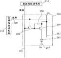
图2是表示显示部所具有的像素的电路结构的一例以及与其周边电路的连接的图。该图中的像素208具备扫描线200、数据线201、电源线202、选择晶体管203、驱动晶体管204、有机EL元件205、保持电容元件206、共用电极207。另外,周边电路具备扫描线驱动电路111、数据线驱动电路112。2 is a diagram illustrating an example of a circuit configuration of a pixel included in a display unit and connections to peripheral circuits thereof. A
扫描线驱动电路111连接于扫描线200,具有控制像素208的选择晶体管203的导通以及非导通的功能。The scanning
数据线驱动电路112连接于数据线201,具有输出数据电压而确定流动于驱动晶体管204的信号电流的功能。The data line driving
选择晶体管203其栅极连接于扫描线200,具有对将数据线201的数据电压供给于驱动晶体管204的栅极的定时进行控制的功能。The
驱动晶体管204作为驱动元件起作用,驱动晶体管204的栅极经由选择晶体管203连接于数据线201,源极连接于有机EL元件205的阳极,漏极连接于电源线202。由此,驱动晶体管204将供给于栅极的数据电压变换为与该数据电压对应的信号电流,将变换后的信号电流供给于有机EL元件205。The driving
有机EL元件205作为发光元件起作用,有机EL元件205的阴极连接于共用电极207。The
保持电容元件206连接于电源线202与驱动晶体管204的栅极端子之间。保持电容元件206具有例如在选择晶体管203变为截止状态之后也维持之前的栅电压并继续使驱动电流从驱动晶体管204向有机EL元件205进行供给的功能。The
另外,在图1、图2中没有记载,但电源线202连接于电源。另外,共用电极207也连接于另外的电源。In addition, although it is not described in FIG. 1 and FIG. 2 , the
从数据线驱动电路112供给的数据电压经由选择晶体管203向驱动晶体管204的栅极端子施加。驱动晶体管204使与该数据电压相应的电流流动于源极-漏极端子之间。通过该电流向有机EL元件205流动,有机EL元件205以与该电流相应的发光辉度发光。The data voltage supplied from the data line driving
接下来,说明实现本发明的有机EL显示装置的制造方法的制造系统。Next, a manufacturing system for realizing the method of manufacturing an organic EL display device of the present invention will be described.
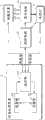
图3是本发明的有机EL显示装置的制造方法中使用的制造系统的功能框图。该图所记载的制造系统具备信息处理装置2、拍摄装置3、电流计4、显示面板11和控制电路12。3 is a functional block diagram of a manufacturing system used in the method of manufacturing an organic EL display device of the present invention. The manufacturing system shown in this figure includes an
信息处理装置2具备运算部21、存储部22、通信部23,具有对直到生成校正参数为止的工序进行控制的功能。作为信息处理装置2,可应用例如个人计算机。The
拍摄装置3根据来自信息处理装置2的通信部23的控制信号,对显示面板11进行拍摄,将所拍摄的图像数据向通信部23输出。作为拍摄装置3,可应用例如CCD照相机和/或辉度计。The
电流计4根据来自信息处理装置2的通信部23以及控制电路12的控制信号,测定在各像素的驱动晶体管204以及有机EL元件205中流动的电流,将所测定的电流值数据向通信部23输出。The
信息处理装置2经由通信部23向有机EL显示装置1内的控制电路12、拍摄装置3以及电流计4输出控制信号,从控制电路12、拍摄装置3以及电流计4获得测定数据而将该测定数据存储于存储部22,基于所存储的测定数据通过运算部21进行运算而计算各种特性值和/或参数。另外,控制电路12也可以使用不内置于有机EL显示装置1的控制电路。The
具体地,在后述的代表电流-电压特性(以下记作代表I-V特性)的设定时,信息处理装置2进行向测定像素提供的电压值的控制以及对在测定像素中流动的电流进行测定的电流计4的控制,接收测定电流值。另外,此时,也可以不设置拍摄装置3。另外,在后述的有机EL元件的辉度-电流特性(以下记作L-I特性)的设定时,信息处理装置2进行向测定像素提供的电压值的控制、拍摄装置3的控制以及电流计4的控制,接收测定辉度值和测定电流值。另外,在各像素的辉度-电压特性(以下记作L-V特性)的设定时,信息处理装置2进行向测定像素提供的电压值的控制、拍摄装置3的控制,接收测定辉度值。Specifically, when setting a representative current-voltage characteristic (hereinafter referred to as representative I-V characteristic) described later, the
控制电路12根据来自信息处理装置2的控制信号,对向显示面板11所具有的像素208提供的电压值进行控制。另外,控制电路12具有将由信息处理装置2生成的校正参数向存储器121写入的功能。The
接下来,说明本发明的有机EL显示装置的制造方法。Next, a method for manufacturing the organic EL display device of the present invention will be described.
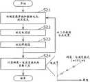
图4是说明本发明的实施方式1所涉及的有机EL显示装置的制造方法的工作流程图。另外,图5A是说明由本发明的实施方式1所涉及的有机EL显示装置的制造方法中的第1工序组得到的特性的图。另外,图5B是说明由本发明的实施方式1所涉及的有机EL显示装置的制造方法中的第2工序组得到的特性的图。另外,图6是说明由本发明的实施方式1所涉及的有机EL显示装置的制造方法中的第3工序组得到的特性的图。FIG. 4 is a flowchart illustrating a method of manufacturing the organic EL display device according to
在图4中,记载了直到生成用于对有机EL显示装置1所具有的显示面板的辉度不均一进行校正的有效的校正参数、将该校正参数存储于有机EL显示装置1内为止的工序。上述有效的校正参数,是为了抑制有机EL元件205的历时劣化而主要对驱动晶体管204的不均一进行校正的参数,但也是不按每像素208进行电流测定而生成的参数。为了生成上述校正参数,在本制造方法中,将显示部113分割为具有多个像素208的分割区域,确定每个该分割区域的L-I特性。另外,该分割区域基于因有机EL元件205的形成工序而产生的显示面板11上的缓慢的辉度倾斜度而进行分割。而且,最终,通过对根据每个分割区域的L-I特性导出的每个像素的I-V特性与代表I-V特性进行比较,生成主要因驱动晶体管204的不均一引起的校正参数。In FIG. 4 , steps up to generating effective correction parameters for correcting the luminance unevenness of the display panel included in the organic
以下,按照图4,对制造工序进行说明。Hereinafter, the manufacturing process will be described with reference to FIG. 4 .
首先,信息处理装置2获得并设定包含多个像素的显示部113整体所共同的代表I-V特性(S01),所述像素包含有机EL元件205和驱动晶体管204,所述有机EL元件205是发光元件,所述驱动晶体管204是对向该有机EL元件的电流的供给进行控制的电压驱动的驱动元件。步骤S01相当于第1步骤。在图5A的(a)中,表示显示部113整体所共同的代表I-V特性。该代表I-V特性是与向驱动晶体管204的栅极施加的电压相对的漏电流的特性,为非线性的特性。First, the
图7A是说明获得代表I-V特性的第1具体方法的工作流程图。在本方法中,从显示部113所具有的多个像素抽出用于确定代表I-V特性的测定用像素。该测定用像素可以是1个,也可以是按照规则性或者随机地选择的多个像素。Fig. 7A is a flowchart illustrating a first concrete method for obtaining representative I-V characteristics. In this method, a measurement pixel for specifying a representative I-V characteristic is extracted from a plurality of pixels included in the
首先,信息处理装置2使控制电路12向测定用像素施加数据电压而使电流流动于该像素,使该像素的有机EL元件205发光(S11)。First, the
接下来,信息处理装置2使电流计4测定步骤S11的电流(S12)。使上述步骤S11以及S12在不同的数据电压下执行多次。另外,可以使上述步骤S11以及S12在多个测定用像素中一齐执行,也可以按每个测定用像素反复执行。Next, the
接下来,信息处理装置2根据在上述步骤S11以及S12得到的数据电压以及对应的电流,通过运算部21求取每个测定用像素的I-V特性(S13)。Next, the
接下来,信息处理装置2通过将对多个测定用像素的各个得到的I-V特性平均化而求取代表I-V特性(S14)。Next, the
图7B是说明获得代表I-V特性的第2具体方法的工作流程图。在本方法中,也从显示部113所具有的多个像素抽出用于确定代表I-V特性的测定用像素。该测定用像素可以是1个,也可以是按照规则性或者随机地选择的多个像素。Fig. 7B is a flowchart illustrating a second specific method for obtaining representative I-V characteristics. Also in this method, a measurement pixel for specifying a representative I-V characteristic is extracted from a plurality of pixels included in the
首先,信息处理装置2使控制电路12向多个测定用像素同时施加共同的数据电压而使电流一齐流动于该多个像素,使该多个像素的有机EL元件205同时发光(S15)。First, the
接下来,信息处理装置2使电流计4测定步骤S15中的各测定用像素的合计电流(S16)。使上述步骤S15以及S16在不同的数据电压下执行多次。Next, the
接下来,信息处理装置2通过运算部21将在上述步骤S15以及S16得到的合计电流值除以多个测定用像素数(S17)。Next, the
接下来,通过使步骤S17按每个数据电压执行,而求取代表I-V特性(S18)。Next, by executing step S17 for each data voltage, representative I-V characteristics are obtained (S18).
通过用图7A以及图7B所记载的方法求取代表I-V特性,由于不是测定显示部113所包含的全部像素的电流,而是仅对多个测定用像素测定电流,所以可以大幅度缩短直至设定显示部113整体所共同的代表I-V特性为止的时间。By obtaining the representative I-V characteristic by the method described in FIG. 7A and FIG. 7B, since the current is not measured for all the pixels included in the
另外,获得代表I-V特性的第1以及第2具体方法也可以不按每个本发明的有机EL显示装置而进行。例如,作为代表I-V特性,也可以将在以同一条件制造的其他有机EL显示装置的制造方法中获得的代表I-V特性直接用作为自身的有机EL显示装置的代表I-V特性。由此,由于将用某一有机EL显示装置的制造方法求取的代表I-V特性用在以与该装置同一条件制造的其他有机EL显示装置的制造方法中,所以可以节省在每次测定多个显示面板的校正参数时都设定代表I-V特性的时间和劳力。结果,可以缩短本装置的制造过程。In addition, the first and second specific methods for obtaining representative I-V characteristics may not be performed for each organic EL display device of the present invention. For example, as representative I-V characteristics, representative I-V characteristics obtained in another method of manufacturing an organic EL display device manufactured under the same conditions may be directly used as representative I-V characteristics of the own organic EL display device. As a result, since the representative I-V characteristics obtained by a certain organic EL display device manufacturing method are used in other organic EL display device manufacturing methods manufactured under the same conditions as the device, it is possible to save multiple measurements in each measurement. The time and labor required to represent the I-V characteristics are set when the calibration parameters of the display panel are set. As a result, the manufacturing process of the device can be shortened.
再次返回到图4,对制造工序进行说明。Returning again to FIG. 4 , the manufacturing process will be described.
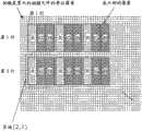
接下来,信息处理装置2将显示面板分割为多个分割区域,使电压施加于各像素所包含的驱动晶体管204,对流动于各分割区域的电流以及此时的从该分割区域的发光辉度进行测定由此求取各分割区域的L-I特性,根据该L-I特性对各分割区域求取L-I变换式(S02)。步骤S02相当于第2步骤。通过执行步骤S02,得到图5A的(b)所记载的各分割区域的L-I特性。该L-I特性以一次函数近似,所述一次函数使用作为发光效率的倒数而定义的倾斜度r以及作为该L-I特性的电流轴截距的发光开始电流值s,以下式表示:Next, the
I=r*L+s (式1)I=r*L+s (Formula 1)
图5A的(c)所记载的矩阵是以式1近似上述的各分割区域的L-I特性而计算的各分割区域的L-I变换式的系数(r,s)。The matrix shown in (c) of FIG. 5A is the coefficient (r, s) of the L-I transformation formula of each divided area calculated by
图8A是说明求取各分割区域的L-I变换式的系数的第1具体方法的工作流程图。在本方法中,从分割区域所具有的多个像素抽出用于确定该分割区域的L-I特性的测定用像素。该测定用像素可以是1个,也可以是按照规则性或者随机地选择的多个像素。另外,也可以是该分割区域所具有的全部像素。Fig. 8A is a flow chart illustrating the operation of a first specific method for obtaining the coefficients of the L-I transform equation for each divided region. In this method, pixels for measurement for specifying the L-I characteristic of the divided region are extracted from a plurality of pixels included in the divided region. The measurement pixel may be one, or may be a plurality of pixels selected regularly or randomly. In addition, all pixels included in the divided region may be used.
首先,信息处理装置2使控制电路12向上述测定用像素一齐施加数据电压而使电流流动于该像素,使该像素的有机EL元件205发光(S21)。First, the
接下来,信息处理装置2使电流计4测定步骤S21的电流(S22)。此时,在测定用像素为分割区域的全部像素的情况下和/或是所选择的多个像素的情况下,测定合计电流值。使上述步骤S21以及S22在不同的数据电压下执行多次。Next, the
接下来,信息处理装置2使拍摄装置3拍摄步骤S21的发光(S23)。使上述步骤S21~S23在不同的数据电压下执行多次。Next, the
接下来,信息处理装置2根据在上述步骤S22以及S23得到的电流以及对应的辉度,通过运算部21求取每个分割区域的L-I特性,按每个分割区域求取上述的L-I变换式的系数(r,s)(S24)。另外,在分割区域所具有的测定用像素为分割区域的全部像素的情况下和/或是所选择的多个像素的情况下,将合计电流值除以测定用像素数而得到的平均电流值作为I而求取每个分割区域的L-I特性。Next, the
图8B是说明求取各分割区域的L-I变换式的系数的第2具体方法的工作流程图。图8B所记载的方法与图8A所记载的方法相比较,仅进行1次步骤S21~S23,仅这一点不同。应用本方法的是假设L-I特性为通过原点的一次式即发光开始电流值s为0的情况。另外,在本方法中,也从分割区域所具有的多个像素抽出用于确定该分割区域的L-I特性的测定用像素。该测定用像素可以是1个,也可以是按照规则性或者随机地选择的多个像素。另外,也可以是该分割区域所具有的全部像素。Fig. 8B is a flow chart illustrating the operation of the second specific method for obtaining the coefficients of the L-I transformation formula for each divided region. The method described in FIG. 8B is different from the method described in FIG. 8A only in that steps S21 to S23 are performed only once. This method is applied on the assumption that the L-I characteristic is a linear expression passing through the origin, that is, the case where the light emission start current value s is zero. Also in this method, pixels for measurement for specifying the L-I characteristic of the divided region are extracted from a plurality of pixels included in the divided region. The measurement pixel may be one, or may be a plurality of pixels selected regularly or randomly. In addition, all pixels included in the divided region may be used.
另外,求取各分割区域的L-I变换式的系数的第1以及第2具体方法也可以不按每个本发明的有机EL显示装置而进行。例如,作为上述系数,也可以将在以同一条件制造的其他有机EL显示装置的制造方法中获得的各分割区域的L-I变换式的系数直接用作为自身的有机EL显示装置的系数。由此,由于将用某一有机EL显示装置的制造方法求取的各分割区域的发光效率以及发光开始电流值用在以与该有机EL显示装置同一条件制造的其他有机EL显示装置的制造方法中,所以可以节省在每次测定多个显示面板的校正参数时都对各显示面板求取各分割区域的发光效率以及发光开始电流值的时间和劳力。结果,可以缩短本装置的制造过程。In addition, the first and second specific methods of obtaining the coefficients of the L-I transformation formula for each divided area may not be performed for each organic EL display device of the present invention. For example, as the above-mentioned coefficients, the coefficients of the L-I conversion formula of each divided region obtained in another method of manufacturing an organic EL display device manufactured under the same conditions may be directly used as coefficients of the own organic EL display device. Therefore, since the luminous efficiency and light emission start current value of each divided region obtained by a method of manufacturing an organic EL display device are used in a method of manufacturing another organic EL display device manufactured under the same conditions as the organic EL display device, Therefore, it is possible to save time and labor for obtaining the luminous efficiency and the luminous start current value of each divided region for each display panel each time the calibration parameters of a plurality of display panels are measured. As a result, the manufacturing process of the device can be shortened.
再次返回到图4,对制造工序进行说明。Returning again to FIG. 4 , the manufacturing process will be described.
接下来,信息处理装置2通过拍摄装置3测定从显示部113所具有的各像素发出的光的辉度,求取各像素的L-V特性(S03)。步骤S03相当于第3步骤。此时,对于各像素的L-V特性,在对每个像素施加电压而测定此时的辉度时,需要像素数的量的测定次数,测定时间以及制造成本大。在本实施方式中,不需要像素数的量的测定次数,可以通过对全部像素一并测定而确定各像素的L-V特性。Next, the
图9A是说明求取各像素的L-V特性的第1具体方法的工作流程图。另外,图9B是说明求取各像素的L-V特性的情况下所拍摄的图像的图。Fig. 9A is a flow chart illustrating the operation of a first specific method for obtaining the L-V characteristic of each pixel. In addition, FIG. 9B is a diagram illustrating an image captured when the L-V characteristic of each pixel is obtained.
首先,信息处理装置2选择要测定的颜色(S31)。在本实施方式中,假定包括像素208的显示部113,所述像素208包括R(红色)、G(绿色)以及B(蓝色)的子像素。First, the
接下来,信息处理装置2选择要测定的灰度等级(S32)。Next, the
接下来,信息处理装置2通过对所选择的颜色的全部子像素施加与所选择的灰度等级相应的电压,使该全部子像素同时发光(S33)。Next, the
接下来,信息处理装置2通过拍摄装置3拍摄从上述全部子像素同时发出的光(S36)。在图9B中,示出选择了红色的情况下拍摄装置3对某灰度等级下的显示部113的发光状态进行拍摄而得到的图像。附图整体所表示的格子图案表示拍摄装置3的受光部的单位像素。由于拍摄装置3的受光部的单位像素相对于所拍摄的R子像素充分小,所以可以根据本图像确定各R子像素的辉度。Next, the
接下来,信息处理装置2改变测定灰度等级(S38中否),执行上述步骤S33以及步骤S36。Next, the
另外,当在全部需要的测定灰度等级下结束了上述步骤S33以及步骤S36的情况下(S38中是),改变测定对象的颜色(S39中否),执行步骤S32~步骤S38。In addition, when the above-mentioned steps S33 and S36 are completed at all required measurement gradations (Yes in S38), the color of the measurement object is changed (No in S39), and steps S32 to S38 are executed.
另外,当在全部颜色下结束了上述步骤S32~步骤S38的情况下(S39中是),信息处理装置2获得在上述步骤S31~步骤S39得到的图像,根据所获得的图像确定各像素的辉度(S40)。在本步骤,例如区域(2,1)的像素的辉度值作为属于区域(2,1)的拍摄元件的像素的输出值的平均值而计算出。In addition, when the above steps S32 to S38 are completed in all colors (Yes in S39), the
根据本方法,不是每当获得每个像素的L-V特性时施加预定的电压而拍摄每个像素的发光,而是一次拍摄发光面板的全部子像素的一齐发光。然后,根据所拍摄的图像,利用将各像素的发光分离的图像处理确定各子像素的发光辉度。因此,由于可以大幅度缩短拍摄时间,所以可以将获得每个像素的L-V特性的工序大幅度简略化。According to this method, light emission of each pixel is captured by applying a predetermined voltage every time the L-V characteristic of each pixel is obtained, but light emission of all sub-pixels of the light emitting panel is captured at once. Then, based on the captured image, the light emission luminance of each sub-pixel is determined by image processing that separates the light emission of each pixel. Therefore, since the imaging time can be greatly shortened, the process of obtaining the L-V characteristic of each pixel can be greatly simplified.
图10A是说明求取各像素的L-V特性的第2具体方法的工作流程图。另外,图10B是说明求取各像素的L-V特性的情况下所拍摄的图像的图。另外,图10C是所选择的测定像素的状态转变图。图10A所记载的方法与图9A所记载的方法相比较,仅附加了步骤S34以及步骤S37这一点不同。即,图10A所记载的方法不是在所选择的颜色以及所选择的灰度等级下使对应的全部子像素一齐发光而获得拍摄图像,而是使该全部子像素的发光分割为多次发光而得到多张拍摄图像。根据本方法,可以避免相邻像素的发光的干扰而计算各像素的高精度的辉度值。Fig. 10A is a flow chart illustrating the operation of a second specific method for obtaining the L-V characteristic of each pixel. In addition, FIG. 10B is a diagram illustrating an image captured when the L-V characteristic of each pixel is obtained. In addition, FIG. 10C is a state transition diagram of selected measurement pixels. The method described in FIG. 10A differs from the method described in FIG. 9A only in that steps S34 and S37 are added. That is, the method described in FIG. 10A does not make all the corresponding sub-pixels emit light at the same time under the selected color and the selected gray scale to obtain a captured image, but divides the light emission of all the sub-pixels into multiple light emission. Get multiple captured images. According to this method, it is possible to calculate a high-precision luminance value of each pixel while avoiding interference of light emission of adjacent pixels.
另外,在图9A以及图10A所示的各像素的L-V特性的计算方法中使用的拍摄装置3优选为图像传感器,进而更优选为CCD照相机。由此,由于可以以低噪音、高灵敏度以及高分辨率获得从全部像素的发光图像,所以可以利用将各像素的发光分离的图像处理获得高精度的各像素的L-V特性。In addition, the
再次返回到图4,对制造工序进行说明。Returning again to FIG. 4 , the manufacturing process will be described.
接下来,信息处理装置2在作为应该生成校正参数的对象的像素不位于与该像素所不属于的其他分割区域的边界的情况下(步骤S04中是),根据在步骤S03设定的各像素的L-V特性和在步骤S02求取的、对象像素所属的分割区域的L-I变换式,求取各像素的I-V特性。即,使用分割区域的L-I特性,将各像素的L-V特性的L参数变换为I,获得各像素的I-V特性。Next, when the pixel to which the correction parameter should be generated is not located at the boundary with another divided area to which the pixel does not belong (Yes in step S04), the
使用图5B的(d),对上述参数变换进行具体说明。例如,在图5A的(c)所记载的系数(r,s)的分割区域矩阵中,属于左上方的分割区域(0,0)(系数(3,15))的像素A的I-V特性如下那样计算出。首先,将在步骤S03获得的像素A的L-V特性的辉度L乘以倾斜度r(即,除以发光效率)。然后,将相乘后的值与发光开始电流值s相加。由此,像素A的L-V特性的参数L被参数变换为反映了各分割区域的L-I特性的I。通过对各像素执行与上述的像素A有关的变换处理,计算出各像素的I-V特性(S05)。步骤S05相当于第4步骤。Using (d) of FIG. 5B , the above-mentioned parameter conversion will be specifically described. For example, in the divided area matrix of coefficients (r, s) described in (c) of FIG. 5A , the I-V characteristics of the pixel A belonging to the upper left divided area (0, 0) (coefficient (3, 15)) are as follows Calculated that way. First, the luminance L of the L-V characteristic of the pixel A obtained in step S03 is multiplied by the inclination r (that is, divided by the luminous efficiency). Then, the multiplied value is added to the light emission start current value s. Thus, the parameter L of the L-V characteristic of the pixel A is parameterized into I reflecting the L-I characteristic of each divided region. The I-V characteristic of each pixel is calculated by performing the above-mentioned conversion processing on the pixel A for each pixel (S05). Step S05 corresponds to the fourth step.
然后,信息处理装置2通过运算部21对各像素计算使在步骤S05求取的各像素的I-V特性成为在步骤S01求取的代表I-V特性的校正参数(S06)。步骤S06相当于第5步骤。Then, the
另一方面,信息处理装置2在作为应该生成校正参数的对象的像素位于与该像素所不属于的其他分割区域的边界附近的情况下(步骤S04中否),根据在步骤S02求取的对象像素所属的分割区域的L-I变换式、上述其他分割区域的L-I变换式和在步骤S03求取的各像素的L-V特性,求取对象像素的I-V特性。使用图11,对上述参数变换进行具体说明。On the other hand, when the pixel to which the correction parameter should be generated is located in the vicinity of the boundary with another divided region to which the pixel does not belong (No in step S04), the
图11是说明对存在于分割区域边界部分的像素的系数进行加权的方法的图。如该图所示,在像素1存在于分割区域1~4的边界区域的情况下,在使用上述步骤S05以及S06生成校正参数时,有可能在校正后的图像中识别出分割区域的边界附近的辉度差。在本方法中,在像素1的校正参数的生成时,不利用像素1所属的分割区域1的L-I变换式的系数(r,s)对像素1的I-V特性进行变换,而利用在相邻的分割区域间进行了倾斜度r以及发光开始电流值s的加权后的L-I变换式的系数(r1,s1)进行变换。在这里,具体地,使用加权后的L-I变换式的系数(r1,s1)计算像素1的I-V特性(S07以及S08)。在图11中,例如,使用相邻的分割区域1~4的系数(r,s),加权后的L-I变换式的系数r1为:FIG. 11 is a diagram illustrating a method of weighting coefficients of pixels existing at the boundary of divided regions. As shown in the figure, when the
r1={(10+8)/2+(14+2)/2}/2=8.5 (式2)r1={(10+8)/2+(14+2)/2}/2=8.5 (Formula 2)
另外,加权后的L-I变换式的系数s1为:In addition, the coefficient s1 of the weighted L-I transformation formula is:
s1={(2+5)/2+(3+4)/2}/2=3.5 (式3)s1={(2+5)/2+(3+4)/2}/2=3.5 (Formula 3)
接下来,信息处理装置2根据在步骤S07加权后的L-I变换式的系数(r1,s1)和在步骤S03获得的像素1的L-V特性,求取像素1的I-V特性。即,将像素1的L-V特性的L,使用加权后的L-I特性,参数变换为I,获得像素1的I-V特性。在该情况下,在系数(r1,s1)的分割区域矩阵中,将在步骤S03获得的像素1的L-V特性的L乘以倾斜度r1。然后,将相乘后的值与发光开始电流值s1相加。由此,像素1的L-V特性的参数L被参数变换为I。通过以上,计算各像素的I-V特性(S08)。步骤S04、S07以及S08相当于第4步骤。Next, the
然后,信息处理装置2通过运算部21对各像素计算使在步骤S08求取的各像素的I-V特性成为在步骤S01求取的代表I-V特性的校正参数(S09)。步骤S09相当于第5步骤。通过步骤S07~S09,可以使配置于分割区域的边界附近的像素间的不均一变得缓和。因此,可以防止在画面上显现出分割区域的边界,可以显示平滑的图像。Then, the
另外,在步骤S07,在求取作为校正对象的像素的倾斜度r1以及发光开始电流值s1时,优选地,该像素越接近于与其他周边分割区域的边界位置,越多考虑该其他周边分割区域的发光效率以及发光开始电流值而进行加权。In addition, in step S07, when obtaining the inclination r1 and the light emission start current value s1 of the pixel to be corrected, it is preferable that the closer the pixel is to the boundary position with other peripheral division regions, the more the other peripheral division regions are considered. Weighting is performed based on the luminous efficiency of the area and the value of the luminous start current.
另外,在步骤S07,在求取作为校正对象的像素的倾斜度r1以及发光开始电流值s1时,也可以根据从该像素到包含该像素的分割区域的中心位置的距离与从该像素到其他周边分割区域的中心位置的距离之比,求取该像素的发光效率以及发光开始电流值。通过这些加权,可以显示更平滑的图像。In addition, in step S07, when obtaining the inclination r1 and the light emission start current value s1 of the pixel to be corrected, the distance from the pixel to the center of the divided region including the pixel and the distance from the pixel to other The ratio of the distances between the center positions of the peripheral divided regions is used to obtain the luminous efficiency and luminous start current value of the pixel. With these weights, smoother images can be displayed.
在这里,对在步骤S06以及步骤S09计算出的校正参数进行说明。Here, the correction parameters calculated in step S06 and step S09 will be described.
图12A是表示本发明的实施方式1所涉及的有机EL显示装置的制造方法中求取电压增益以及电压偏移的校正值的情况下的电流-电压特性的曲线图。在该图中,校正参数包含电压增益,该电压增益表示在上述步骤S05或者S08求取的作为校正对象的像素的I-V特性的电压值与在步骤S01设定的代表I-V特性的电压值之比。进而,图12A所记载的校正参数包含电压偏移,该电压偏移表示在上述步骤S05或者S08求取的作为校正对象的像素的I-V特性的电压值与在步骤S01设定的代表I-V特性的电压值之差。12A is a graph showing current-voltage characteristics when correction values for voltage gain and voltage offset are obtained in the method of manufacturing the organic EL display device according to
图12B是表示本发明的实施方式1所涉及的有机EL显示装置的制造方法中求取电压增益的校正值的情况下的电流-电压特性的曲线图。在该图中,校正参数包含电流增益,该电流增益表示在上述步骤S05或者S08求取的作为校正对象的像素的I-V特性的电流值与在步骤S01设定的代表I-V特性的电流值之比。12B is a graph showing current-voltage characteristics when a correction value of a voltage gain is obtained in the method of manufacturing the organic EL display device according to
另外,上述校正参数并不限定于图12A以及图12B所记载的组合,而只要是包含电压增益、电压偏移以及电流增益这3种之中的至少1种的构成即可。In addition, the above-mentioned correction parameters are not limited to the combinations described in FIG. 12A and FIG. 12B , and any configuration including at least one of voltage gain, voltage offset, and current gain may be used.
再次返回到图4,对制造工序进行说明。Returning again to FIG. 4 , the manufacturing process will be described.
最后,信息处理装置2将在上述步骤S06以及S09求取的各像素的校正参数写入有机EL显示装置1的存储器121(S10)。步骤S10相当于第6步骤。具体地,如图6的(f)所记载,在存储器121中,与显示部113(M行×N列)的矩阵对应地存储例如按每个像素包括(电压增益、电压偏移)的校正参数。Finally, the
在本发明的有机EL显示装置的制造方法中,将所测定的各像素的L-V特性的辉度值除以表示在各分割区域内所共同的特性的发光效率,并将该除法值与发光开始电流值相加而求取各像素的I-V特性。因此,与求取用于将各像素的L-V特性校正为显示面板所共同的代表L-V特性的校正参数的情况相比,由各像素的校正参数产生的校正量变小。这是因为,各像素的L-V特性包含驱动晶体管以及有机EL元件的不均一双方,相对于此,通过上述的方法计算出的各像素的I-V特性主要仅包含驱动晶体管的不均一。因此,各像素的校正参数的值的范围变小,可以减少对校正参数的值分配的存储器的位数。结果,可以减小存储器121的容量,可以降低制造成本。In the manufacturing method of the organic EL display device of the present invention, the luminance value of the measured L-V characteristic of each pixel is divided by the luminous efficiency representing the characteristic common in each divided area, and the divided value is compared with the emission start The current values are added to obtain the I-V characteristic of each pixel. Therefore, the correction amount by the correction parameter of each pixel is smaller than that obtained in the case of calculating the correction parameter for correcting the L-V characteristic of each pixel to represent the L-V characteristic common to the display panel. This is because the L-V characteristics of each pixel include variations in both the driving transistor and the organic EL element, whereas the I-V characteristics of each pixel calculated by the method described above mainly include only variations in the driving transistor. Therefore, the value range of the correction parameter of each pixel is narrowed, and the number of bits of memory allocated to the value of the correction parameter can be reduced. As a result, the capacity of the
在以往的校正参数的生成方法中,测定从显示面板所包含的各像素发出的光的辉度而求取的各像素的辉度-电压特性反映有机EL元件的不均一以及驱动晶体管的不均一双方。在求取对于这双方的不均一进行校正的校正参数、使用该校正参数对来自外部的影像信号进行校正的情况下,该校正为包含了有机EL元件的不均一的校正。因此,根据该校正,显示面板整体对于同一灰度等级的影像信号从有机EL元件发出的光的辉度变得均等。In the conventional method of generating correction parameters, the luminance-voltage characteristics of each pixel obtained by measuring the luminance of light emitted from each pixel included in the display panel reflect the unevenness of the organic EL element and the unevenness of the driving transistor. both sides. When a correction parameter for correcting both of the unevennesses is obtained and an external video signal is corrected using the correction parameters, the correction includes the unevenness of the organic EL element. Therefore, according to this correction, the luminance of light emitted from the organic EL elements becomes equal for the entire display panel with respect to video signals of the same gradation level.
但是,由于有机EL元件的特性不均一,流动同一电流的情况下的辉度在有机EL元件间不同,所以流动于有机EL元件的电流量会变化。因此,在该情况下,从有机EL元件的寿命依赖于电流量的观点来看,随着时间经过,各发光元件的寿命会变得不均一。该寿命的不均一结果作为辉度不均而表现在画面上。However, since the characteristics of the organic EL elements are not uniform, the luminance when the same current flows varies among the organic EL elements, so the amount of current flowing through the organic EL elements varies. Therefore, in this case, from the viewpoint that the lifetime of the organic EL element depends on the amount of current, the lifetime of each light emitting element becomes non-uniform over time. The result of this unevenness in lifetime appears on the screen as unevenness in luminance.
因此,在本方式中,仅对驱动晶体管的不均一进行校正,将对于同一灰度等级的影像信号而流动于各有机EL元件的电流量设定为均等。这是因为,驱动晶体管的不均一在各元件间较大,但有机EL元件的不均一在各元件间非常小,只要可以仅对驱动晶体管的不均一进行校正,即使不校正有机EL元件的不均一,也可以显示对于人眼而言均匀的图像。Therefore, in this embodiment, only the unevenness of the driving transistors is corrected, and the amount of current flowing to each organic EL element is set to be equal for video signals of the same gray scale. This is because the unevenness of the driving transistor is large among the elements, but the unevenness of the organic EL element is very small among the elements. As long as only the unevenness of the driving transistor can be corrected, even if the unevenness of the organic EL element is not corrected, the unevenness of the organic EL element can be corrected. Uniform, can also display an image that is uniform to the human eye.
根据本实施方式,包含作为校正对象的像素的分割区域的L-I特性是包含有机EL元件的不均一的特性。因此,使用包含作为校正对象的像素的分割区域的L-I特性将作为校正对象的像素的L-V特性变换成各像素的I-V特性,指的是求取主要对驱动晶体管的不均一进行校正的校正参数。According to the present embodiment, the L-I characteristic of the divided region including the pixel to be corrected is a characteristic including non-uniformity of the organic EL element. Therefore, converting the L-V characteristic of the pixel to be corrected into the I-V characteristic of each pixel using the L-I characteristic of the divided region including the pixel to be corrected refers to obtaining correction parameters mainly for correcting the unevenness of the driving transistor.
图13是说明用本发明的有机EL显示装置的制造方法校正后的有机EL显示装置的效果的图。在校正前,有机EL显示装置的显示面板具有反映了因有机EL元件引起的辉度分布和因驱动晶体管引起的辉度分布双方的辉度分布。与此相对,在本发明的有机EL显示装置的制造方法中,由于主要对驱动晶体管的不均一进行校正,所以校正后的显示面板虽然还残留由有机EL元件的特性不均一引起的辉度倾斜度,但可以对于指定的同一灰度等级将流动于各有机EL元件的电流设定为一定,所以可以将在有机EL元件间施加的电流负荷设定为一定。因此,可以将流动于各有机EL元件的电流设定为均等,可以抑制所述显示面板所包含的各发光元件的寿命随着时间经过而变得不均一。结果,可以防止在画面上显示因各发光元件的寿命的不均一引起的辉度不均。另外,在校正后的显示面板残存的、由有机EL元件的特性不均一引起的辉度倾斜度为人的视觉不会识别出的辉度倾斜度。FIG. 13 is a diagram illustrating the effect of the organic EL display device corrected by the method of manufacturing the organic EL display device of the present invention. Before correction, the display panel of the organic EL display device has a luminance distribution reflecting both the luminance distribution due to the organic EL element and the luminance distribution due to the driving transistor. On the other hand, in the method of manufacturing the organic EL display device of the present invention, since the unevenness of the driving transistor is mainly corrected, the corrected display panel still has the luminance gradient caused by the unevenness of the characteristics of the organic EL element. However, the current flowing through each organic EL element can be set constant for the same designated gray scale, so the current load applied between the organic EL elements can be set constant. Therefore, the current flowing to each organic EL element can be set to be equal, and the lifetime of each light emitting element included in the display panel can be suppressed from becoming uneven over time. As a result, it is possible to prevent uneven luminance from being displayed on the screen due to the uneven lifetime of the light emitting elements. In addition, the luminance gradient caused by the characteristic unevenness of the organic EL element remaining in the corrected display panel is a luminance gradient that cannot be recognized by human vision.
另外,在本方式中,为了得到用于对驱动晶体管的不均一进行校正的校正参数,不是测定各像素中的驱动晶体管的不均一本身,而是测定各像素的包含有机EL元件的不均一以及驱动晶体管的不均一双方的L-V特性和各分割区域的有机EL元件的发光效率以及发光开始电流值。即,各分割区域的发光效率以及发光开始电流值,通过将显示面板分割为多个分割区域并对各分割区域测定流动于各分割区域的电流以及流动该电流时的辉度而求取。换而言之,通过求取各分割区域的发光效率以及发光开始电流值,可以掌握各分割区域间的发光元件的不均一。这是因为,有机EL元件与其说按每像素不如说按每某一定的区域变得不均一。另外,各像素的L-V特性,通过使用CCD照相机等,可以同时测定多个像素。由此,与对各像素施加电压、通过测定流动于各像素的电流而测定驱动晶体管的不均一的情况相比,可以大幅度缩短校正参数的测定时间。In addition, in this form, in order to obtain the correction parameters for correcting the unevenness of the driving transistor, the unevenness of the driving transistor in each pixel is not measured, but the unevenness including the organic EL element of each pixel and Both the L-V characteristics of the drive transistor and the luminous efficiency and luminous start current value of the organic EL element in each divided region vary. That is, the luminous efficiency and light emission start current value of each divided region are obtained by dividing the display panel into a plurality of divided regions and measuring the current flowing in each divided region and the luminance when the current flows. In other words, by obtaining the luminous efficiency and light emission start current value of each divided region, it is possible to grasp the unevenness of the light emitting element among the divided regions. This is because the organic EL element becomes non-uniform every certain area rather than every pixel. In addition, the L-V characteristic of each pixel can be measured at the same time by using a CCD camera or the like. This makes it possible to greatly shorten the measurement time of the correction parameters, compared to the case where the unevenness of the drive transistor is measured by applying a voltage to each pixel and measuring the current flowing through each pixel.
另外,在本发明的有机EL显示装置的制造方法中,将显示面板分割为分割区域,但该分割优选为反映了由有机EL元件的特性不均一引起的辉度倾斜度的分割。In addition, in the method of manufacturing the organic EL display device of the present invention, the display panel is divided into divided regions, but the division is preferably a division that reflects the gradient of luminance due to the characteristic non-uniformity of the organic EL element.
图14A是表示通过蒸镀形成了发光层的情况下的显示面板上的辉度分布的图。在通过蒸镀形成了发光层的情况下,显示部113的中央部的发光层膜厚变厚,产生同心圆状的膜厚分布。因此,有机EL元件的发光效率以及发光开始电流值具有同心圆状的分布。在该情况下,通过将分割区域分割为图14A所示的同心圆状,结果,可以高精度地得到用于主要对驱动晶体管204的不均一进行校正的校正参数。FIG. 14A is a diagram showing a luminance distribution on a display panel when a light emitting layer is formed by vapor deposition. When the light-emitting layer is formed by vapor deposition, the film thickness of the light-emitting layer becomes thicker in the central portion of the
另一方面,图14B是表示通过喷墨印刷形成了发光层的情况下的显示面板上的辉度分布的图。在扫描喷墨头、对显示部113印刷发光层的情况下,因墨干燥时的环境的不同等,在扫描方向发光效率发生变化。另外,各喷墨头的喷嘴的射出量在喷墨头的长轴方向缓慢地变得不均一,由此在与扫描方向垂直的方向,发光效率也发生变化。在这样的发光效率分布不单调的情况下,优选对分割区域细致地进行分割。由此,结果,可以高精度地得到用于主要对驱动晶体管的不均一进行校正的校正参数。On the other hand, FIG. 14B is a diagram showing the luminance distribution on the display panel when the light emitting layer is formed by inkjet printing. When the inkjet head is scanned to print the light emitting layer on the
(实施方式2)(Embodiment 2)
在本实施方式中,对于有机EL显示装置使用利用本发明的有机EL显示装置的制造方法生成的校正参数使显示面板进行显示工作的情况进行说明。In this embodiment, a case where an organic EL display device performs a display operation on a display panel using calibration parameters generated by the method for manufacturing an organic EL display device of the present invention will be described.
图15是说明本发明的实施方式2所涉及的有机EL显示装置的显示工作时的电压增益以及电压偏移的校正工作的图。15 is a diagram illustrating a voltage gain and a voltage offset correction operation during a display operation of the organic EL display device according to
控制电路12从存储器121读取例如在实施方式1存储的校正参数(电压增益、电压偏移),将与影像信号对应的数据电压乘以电压增益,然后将相乘值与电压偏移相加,向数据线驱动电路112输出。由此,由于可以对于指定的同一灰度等级将流动于多个有机EL元件的各个的电流设定为一定,所以可以将在有机EL元件间施加的电流负荷设定为一定。因此,可以将流动于各有机EL元件的电流设定为均等,可以抑制显示面板所包含的各有机EL元件的寿命随着时间经过而变得不均一。结果,可以防止在画面上显示因各有机EL元件的寿命的不均一引起的辉度不均。The
图16是说明本发明的实施方式2所涉及的有机EL显示装置的显示工作时的电流增益的校正工作的图。16 is a diagram illustrating a correction operation of a current gain during a display operation of the organic EL display device according to
控制电路101将从外部输入的影像信号校正变换为与各像素对应的电压信号。存储器102存储与各像素部对应的电流增益以及代表LUT。The
该图中的控制电路101具备校正块601和变换块602。校正块601在影像信号从外部输入时,对于所输入的a行b列的像素的电流信号从存储器102读取a行b列的电流增益(k)而进行运算,对该电流信号进行校正。变换块602基于存储于存储器102的代表变换曲线,将上述校正后的电流信号变换为与该影像信号对应的a行b列的电压信号。校正块601具备像素位置检测部611、影像-电流变换部612和乘法部613,变换块602具备电流-电压变换部614和驱动电路用定时控制器615。The
像素位置检测部611根据与从外部输入的影像信号同时输入的同步信号,检测该影像信号的像素位置信息。在这里,假定所检测出的像素位置为a行b列。The pixel
影像-电流变换部612从存储于存储器102的影像-电流变换LUT,读取与该影像信号对应的电流信号。The video-to-
乘法部613通过将在实施方式1存储于存储器102的与各像素部对应的电流增益与该电流信号相乘,而对该电流信号进行校正。具体地,将a行b列的电流增益与a行b列的电流信号值相乘,生成校正后的a行b列的电流信号。The
另外,乘法部613也可以通过将在实施方式1存储于存储器102的与各像素部对应的电流增益与对从外部输入的影像信号进行变换而成的电流信号相除等乘法以外的运算,对该电流信号进行校正。In addition, the
电流-电压变换部614从基于存储于存储器102的代表变换曲线导出的代表LUT,读取与从乘法部613输出的校正后的a行b列的电流信号对应的a行b列的电压信号。The current-
最后,控制电路101将该变换后的a行b列的电压信号经由驱动电路用定时控制器615,向数据线驱动电路112输出。该电压信号被变换为模拟电压而向数据线驱动电路输入,或者在数据线驱动电路内被变换为模拟电压。然后,从数据线驱动电路112,作为数据电压向各像素供给。Finally, the
根据本方式,利用校正块601以及变换块602,按每像素部将从外部输入的影像信号变换为电流信号,将每像素部的电流信号校正为预定的基准电流。在此基础上,将校正后的各像素部的电流信号变换为电压信号,将该变换后的电压信号向数据线的驱动电路输出。According to this embodiment, the
由此,按每像素部存储的数据为与各像素部对应的电流增益并且是用于将与各像素部对应的影像信号的电流设定为预定的基准电流的电流增益。因此,不需要按每像素部准备以往那样的将与影像信号对应的电流信号变换为电压信号的电流信号-电压信号变换表,可以大幅度削减按每像素部准备的数据量。而且,使与代表变换曲线对应的预定的信息为所述多个像素部所共有,所述代表变换曲线表示所述多个像素部所共同的电压-电流特性。这也可以使数据量为很少。Thus, the data stored for each pixel unit is the current gain corresponding to each pixel unit and is the current gain for setting the current of the video signal corresponding to each pixel unit to a predetermined reference current. Therefore, there is no need to prepare a conventional current signal-voltage signal conversion table for converting a current signal corresponding to a video signal into a voltage signal for each pixel unit, and the amount of data prepared for each pixel unit can be significantly reduced. Furthermore, predetermined information corresponding to a representative conversion curve representing a voltage-current characteristic common to the plurality of pixel units is shared by the plurality of pixel units. This also keeps data volumes to a minimum.
因此,可以使校正所需要的数据的量大幅度减少,所述校正是用于按显示面板的每像素部对不均一的电流进行校正而得到在整个画面所共同的电流的影像信号的校正。由此,可以大幅度削减制造成本。结果,可以降低制造成本以及驱动时的处理负担,遍及画面整体实现均匀的显示。Therefore, it is possible to significantly reduce the amount of data required for correction of video signals for correcting non-uniform current for each pixel portion of the display panel to obtain a current common to the entire screen. Thereby, manufacturing cost can be reduced significantly. As a result, the manufacturing cost and the processing load at the time of driving can be reduced, and a uniform display can be realized over the entire screen.
另外,由于表示与多个像素部所共同的电压-电流特性对应的代表变换曲线的预定的信息对于多个像素部相同而为一个,所以可以将存储器容量削减到必要的最小限度。In addition, since the predetermined information indicating the representative conversion curve corresponding to the voltage-current characteristic common to the plurality of pixel units is the same for the plurality of pixel units, the memory capacity can be reduced to the necessary minimum.
在这里,在上述校正块601中使用的电流增益是用本发明的有机EL显示装置的制造方法生成、存储于存储器的校正参数。另外,代表变换曲线也可以是在本发明的有机EL显示装置的制造方法中的步骤S01设定的代表I-V特性。Here, the current gain used in the
在图16所记载的将电流增益作为校正参数的情况下,由于也可以将对于指定的同一灰度等级而流动于多个有机EL元件的各个的电流成为一定,所以可以将在有机EL元件间施加的电流负荷成为一定。因此,可以使流动于各有机EL元件的电流变得均等,可以抑制显示面板所包含的各有机EL元件的寿命随着时间经过而变得不均一。结果,可以防止在画面上显示因各有机EL元件的寿命的不均一引起的辉度不均。In the case of using the current gain as the correction parameter described in FIG. 16 , since the currents flowing in each of the organic EL elements can be made constant for the same designated gray level, it is possible to set the current gain between the organic EL elements The applied current load becomes constant. Therefore, the electric current flowing through each organic EL element can be made equal, and it can suppress that the lifetime of each organic EL element included in a display panel becomes uneven with time. As a result, it is possible to prevent uneven luminance from being displayed on the screen due to the uneven lifetime of the organic EL elements.
以上对于实施方式1以及2进行了描述,但本发明所涉及的有机EL显示装置及其制造方法并不限定于上述实施方式。对上述的实施方式在不脱离本发明的主旨的范围内实施本领域技术人员所想出的各种变形而得到的变形例和/或内置有本发明所涉及的有机EL显示装置的各种设备也包含于本发明。Embodiments 1 and 2 have been described above, but the organic EL display device and its manufacturing method according to the present invention are not limited to the above embodiments. Modified examples obtained by implementing various modifications conceived by those skilled in the art to the above-mentioned embodiments without departing from the gist of the present invention, and/or various devices incorporating the organic EL display device according to the present invention It is also included in the present invention.
例如,本发明所涉及的有机EL显示装置及其制造方法可内置于图17所记载那样的薄型平板TV。利用本发明所涉及的有机EL显示装置及其制造方法,可以实现具备抑制了辉度不均的长寿命显示器的低成本薄型平板TV。For example, the organic EL display device and its manufacturing method according to the present invention can be incorporated in a thin flat-panel TV as shown in FIG. 17 . According to the organic EL display device and its manufacturing method according to the present invention, it is possible to realize a low-cost thin flat-panel TV including a long-life display with suppressed luminance unevenness.
本发明对于内置有机EL显示装置的有机EL平板显示器特别有用,最适于用作为要求画质的均匀性的显示器的显示装置及其制造方法。The present invention is particularly useful for an organic EL flat panel display with a built-in organic EL display device, and is most suitable for use as a display device and a manufacturing method thereof as a display requiring uniformity of image quality.
Claims (15)
Applications Claiming Priority (3)
| Application Number | Priority Date | Filing Date | Title |
|---|---|---|---|
| JP2010070960AJP5560076B2 (en) | 2010-03-25 | 2010-03-25 | Organic EL display device and manufacturing method thereof |
| JP070960/2010 | 2010-03-25 | ||
| PCT/JP2011/000844WO2011118124A1 (en) | 2010-03-25 | 2011-02-16 | Organic electroluminescence display apparatus and production method for same |
Publications (2)
| Publication Number | Publication Date |
|---|---|
| CN102428509Atrue CN102428509A (en) | 2012-04-25 |
| CN102428509B CN102428509B (en) | 2014-08-13 |
Family
ID=44672705
Family Applications (1)
| Application Number | Title | Priority Date | Filing Date |
|---|---|---|---|
| CN201180001813.7AActiveCN102428509B (en) | 2010-03-25 | 2011-02-16 | Organic EL display device and manufacturing method thereof |
Country Status (5)
| Country | Link |
|---|---|
| US (1) | US9208721B2 (en) |
| JP (1) | JP5560076B2 (en) |
| KR (1) | KR101276456B1 (en) |
| CN (1) | CN102428509B (en) |
| WO (1) | WO2011118124A1 (en) |
Cited By (1)
| Publication number | Priority date | Publication date | Assignee | Title |
|---|---|---|---|---|
| CN107705740A (en)* | 2016-08-09 | 2018-02-16 | 株式会社日本有机雷特显示器 | Bearing calibration, manufacture method and the display methods of display device and display device |
Families Citing this family (15)
| Publication number | Priority date | Publication date | Assignee | Title |
|---|---|---|---|---|
| WO2013129611A1 (en)* | 2012-02-29 | 2013-09-06 | 昭和電工株式会社 | Manufacturing method for electroluminescent element |
| KR20140122362A (en)* | 2013-04-09 | 2014-10-20 | 삼성디스플레이 주식회사 | Display device and driving method thereof |
| KR101461995B1 (en)* | 2013-05-14 | 2014-11-24 | (주)코텍 | Apparatus for compensating brightness uniformity of flat panel display and the method therof |
| KR102162499B1 (en) | 2014-02-26 | 2020-10-08 | 삼성디스플레이 주식회사 | Organic light emitting display and method for driving the same |
| US10276095B2 (en) | 2014-08-21 | 2019-04-30 | Joled Inc. | Display device and method of driving display device |
| KR102366198B1 (en)* | 2014-12-08 | 2022-02-23 | 엘지디스플레이 주식회사 | Display Device and Driving Method Thereof |
| US10217408B2 (en) | 2015-11-11 | 2019-02-26 | Joled Inc. | Display device, display device correction method, display device manufacturing method, and display device display method |
| US10283044B2 (en) | 2015-11-11 | 2019-05-07 | Joled Inc. | Display device, display device correction method, display device manufacturing method, and display device display method |
| JP6744791B2 (en) | 2015-11-11 | 2020-08-19 | 株式会社Joled | Display device, display device correction method, display device manufacturing method, and display device display method |
| KR102707620B1 (en)* | 2016-08-31 | 2024-09-20 | 엘지디스플레이 주식회사 | Display and driving method for the same |
| JP6755773B2 (en) | 2016-10-28 | 2020-09-16 | 株式会社Joled | Display device, display device correction method, display device manufacturing method, and display device display method. |
| TWI748035B (en)* | 2017-01-20 | 2021-12-01 | 日商半導體能源硏究所股份有限公司 | Display system and electronic device |
| WO2018186613A1 (en)* | 2017-04-07 | 2018-10-11 | 이승원 | Driver ic device including correction function |
| KR20220085118A (en) | 2020-12-14 | 2022-06-22 | 삼성디스플레이 주식회사 | Display apparatus and method of driving the same |
| KR20230016131A (en) | 2021-07-23 | 2023-02-01 | 삼성디스플레이 주식회사 | Display manufacturing system and driving method of the same |
Citations (4)
| Publication number | Priority date | Publication date | Assignee | Title |
|---|---|---|---|---|
| JPH11219146A (en)* | 1997-09-29 | 1999-08-10 | Mitsubishi Chemical Corp | Active matrix light emitting diode pixel structure and method |
| CN1664899A (en)* | 2004-03-04 | 2005-09-07 | 精工爱普生株式会社 | Electro-optical device, driving circuit and driving method thereof, and electronic apparatus |
| US20060284802A1 (en)* | 2005-06-15 | 2006-12-21 | Makoto Kohno | Assuring uniformity in the output of an oled |
| US20070008251A1 (en)* | 2005-07-07 | 2007-01-11 | Makoto Kohno | Method of correcting nonuniformity of pixels in an oled |
Family Cites Families (13)
| Publication number | Priority date | Publication date | Assignee | Title |
|---|---|---|---|---|
| JP2002055675A (en) | 1999-09-17 | 2002-02-20 | Matsushita Electric Ind Co Ltd | Image display device |
| US6791566B1 (en) | 1999-09-17 | 2004-09-14 | Matsushita Electric Industrial Co., Ltd. | Image display device |
| SG107573A1 (en)* | 2001-01-29 | 2004-12-29 | Semiconductor Energy Lab | Light emitting device |
| JP3854161B2 (en)* | 2002-01-31 | 2006-12-06 | 株式会社日立製作所 | Display device |
| CN101325024B (en) | 2003-03-27 | 2011-02-16 | 三洋电机株式会社 | Display irregularity correction method |
| JP2005283816A (en) | 2004-03-29 | 2005-10-13 | Seiko Epson Corp | Electro-optical device, electro-optical device driving method, electro-optical device manufacturing method, and electronic apparatus |
| JP4855648B2 (en) | 2004-03-30 | 2012-01-18 | グローバル・オーエルイーディー・テクノロジー・リミテッド・ライアビリティ・カンパニー | Organic EL display device |
| JP2009169071A (en)* | 2008-01-16 | 2009-07-30 | Sony Corp | Display device |
| CN101765874B (en) | 2008-05-28 | 2014-09-10 | 松下电器产业株式会社 | Display device, manufacturing method and control method of display device |
| JP2010134169A (en)* | 2008-12-04 | 2010-06-17 | Panasonic Corp | Active matrix type display apparatus, inspecting method and method for manufacturing such display apparatus |
| US8130182B2 (en)* | 2008-12-18 | 2012-03-06 | Global Oled Technology Llc | Digital-drive electroluminescent display with aging compensation |
| JP5280291B2 (en)* | 2009-04-28 | 2013-09-04 | シャープ株式会社 | Organic EL active matrix driving method, driving circuit, and display device |
| JP5804263B2 (en)* | 2010-10-08 | 2015-11-04 | 三菱化学株式会社 | Lighting device control method |
- 2010
- 2010-03-25JPJP2010070960Apatent/JP5560076B2/enactiveActive
- 2011
- 2011-02-16CNCN201180001813.7Apatent/CN102428509B/enactiveActive
- 2011-02-16WOPCT/JP2011/000844patent/WO2011118124A1/enactiveApplication Filing
- 2011-02-16KRKR1020117024667Apatent/KR101276456B1/ennot_activeExpired - Fee Related
- 2012
- 2012-09-17USUS13/621,351patent/US9208721B2/enactiveActive
Patent Citations (4)
| Publication number | Priority date | Publication date | Assignee | Title |
|---|---|---|---|---|
| JPH11219146A (en)* | 1997-09-29 | 1999-08-10 | Mitsubishi Chemical Corp | Active matrix light emitting diode pixel structure and method |
| CN1664899A (en)* | 2004-03-04 | 2005-09-07 | 精工爱普生株式会社 | Electro-optical device, driving circuit and driving method thereof, and electronic apparatus |
| US20060284802A1 (en)* | 2005-06-15 | 2006-12-21 | Makoto Kohno | Assuring uniformity in the output of an oled |
| US20070008251A1 (en)* | 2005-07-07 | 2007-01-11 | Makoto Kohno | Method of correcting nonuniformity of pixels in an oled |
Cited By (2)
| Publication number | Priority date | Publication date | Assignee | Title |
|---|---|---|---|---|
| CN107705740A (en)* | 2016-08-09 | 2018-02-16 | 株式会社日本有机雷特显示器 | Bearing calibration, manufacture method and the display methods of display device and display device |
| CN107705740B (en)* | 2016-08-09 | 2021-05-11 | 株式会社日本有机雷特显示器 | Display device, and calibration method, manufacturing method, and display method of display device |
Also Published As
| Publication number | Publication date |
|---|---|
| CN102428509B (en) | 2014-08-13 |
| US9208721B2 (en) | 2015-12-08 |
| US20130021389A1 (en) | 2013-01-24 |
| KR20120023615A (en) | 2012-03-13 |
| WO2011118124A1 (en) | 2011-09-29 |
| JP5560076B2 (en) | 2014-07-23 |
| JP2011203509A (en) | 2011-10-13 |
| KR101276456B1 (en) | 2013-06-19 |
Similar Documents
| Publication | Publication Date | Title |
|---|---|---|
| CN102428510B (en) | Organic El Display Apparatus And Production Method For The Same | |
| CN102428509B (en) | Organic EL display device and manufacturing method thereof | |
| US10460639B2 (en) | Luminance compensation system and luminance compensation method thereof | |
| JP5443504B2 (en) | Method for providing drive transistor control signal to drive transistor | |
| CN101765874B (en) | Display device, manufacturing method and control method of display device | |
| US9135887B2 (en) | Display device and driving method of the same | |
| JP5552117B2 (en) | Display method for organic EL display device and organic EL display device | |
| KR101272367B1 (en) | Calibration System of Image Display Device Using Transfer Functions And Calibration Method Thereof | |
| TWI449017B (en) | Electroluminescent display with initial nonuniformity compensation | |
| KR102138590B1 (en) | Apparatus and Method for Generating of Luminance Correction Data | |
| TW201033973A (en) | Electroluminescent display initial-nonuniformity-compensated drive signal | |
| WO2022160496A1 (en) | Display compensation method, display compensation device and display device | |
| JP2010134169A (en) | Active matrix type display apparatus, inspecting method and method for manufacturing such display apparatus | |
| JP5995165B2 (en) | Display device inspection method, inspection device, and manufacturing method | |
| JP2016009136A (en) | Display device and manufacturing method of the same | |
| KR102281009B1 (en) | Orgainc emitting diode display device and method for driving the same | |
| WO2011125112A1 (en) | Organic el display device manufacturing method and organic el display device | |
| WO2011125108A1 (en) | Method for manufacturing organic el display device, and organic el display device |
Legal Events
| Date | Code | Title | Description |
|---|---|---|---|
| C06 | Publication | ||
| PB01 | Publication | ||
| C10 | Entry into substantive examination | ||
| SE01 | Entry into force of request for substantive examination | ||
| C14 | Grant of patent or utility model | ||
| GR01 | Patent grant | ||
| ASS | Succession or assignment of patent right | Owner name:JANPAN ORGANIC RATE DISPLAY CO., LTD. Free format text:FORMER OWNER: MATSUSHITA ELECTRIC INDUSTRIAL CO, LTD. Effective date:20150826 | |
| C41 | Transfer of patent application or patent right or utility model | ||
| TR01 | Transfer of patent right | Effective date of registration:20150826 Address after:Tokyo, Japan Patentee after:JOLED Inc. Address before:Osaka Japan Patentee before:Matsushita Electric Industrial Co.,Ltd. | |
| TR01 | Transfer of patent right | Effective date of registration:20231204 Address after:Tokyo, Japan Patentee after:Japan Display Design and Development Contract Society Address before:Tokyo, Japan Patentee before:JOLED Inc. | |
| TR01 | Transfer of patent right | ||
| TR01 | Transfer of patent right | Effective date of registration:20250728 Address after:Tokyo, Japan Patentee after:Magno Bolan Co.,Ltd. Country or region after:Japan Address before:Tokyo, Japan Patentee before:Japan Display Design and Development Contract Society Country or region before:Japan | |
| TR01 | Transfer of patent right |