CN102426306A - Ultrafast electronic device test system and method - Google Patents
Ultrafast electronic device test system and methodDownload PDFInfo
- Publication number
- CN102426306A CN102426306ACN2011102693063ACN201110269306ACN102426306ACN 102426306 ACN102426306 ACN 102426306ACN 2011102693063 ACN2011102693063 ACN 2011102693063ACN 201110269306 ACN201110269306 ACN 201110269306ACN 102426306 ACN102426306 ACN 102426306A
- Authority
- CN
- China
- Prior art keywords
- ultrafast
- femtosecond
- pulse
- electronic device
- fiber
- Prior art date
- Legal status (The legal status is an assumption and is not a legal conclusion. Google has not performed a legal analysis and makes no representation as to the accuracy of the status listed.)
- Granted
Links
- 238000012360testing methodMethods0.000titleclaimsabstractdescription45
- 238000000034methodMethods0.000titleclaimsabstractdescription8
- 239000013078crystalSubstances0.000claimsabstractdescription69
- 230000004044responseEffects0.000claimsabstractdescription29
- 238000001514detection methodMethods0.000claimsabstractdescription18
- 238000005259measurementMethods0.000claimsabstractdescription12
- 230000005684electric fieldEffects0.000claimsabstractdescription10
- 238000012937correctionMethods0.000claimsabstractdescription6
- 239000000835fiberSubstances0.000claimsdescription59
- 230000008878couplingEffects0.000claimsdescription40
- 238000010168coupling processMethods0.000claimsdescription40
- 238000005859coupling reactionMethods0.000claimsdescription40
- 239000013307optical fiberSubstances0.000claimsdescription21
- 230000003287optical effectEffects0.000claimsdescription19
- 230000010287polarizationEffects0.000claimsdescription13
- JBRZTFJDHDCESZ-UHFFFAOYSA-NAsGaChemical compound[As]#[Ga]JBRZTFJDHDCESZ-UHFFFAOYSA-N0.000claimsdescription8
- 229910017214AsGaInorganic materials0.000claimsdescription8
- 229910007709ZnTeInorganic materials0.000claimsdescription8
- 238000006243chemical reactionMethods0.000claimsdescription6
- 229910013641LiNbO 3Inorganic materials0.000claimsdescription2
- 238000012544monitoring processMethods0.000claimsdescription2
- 230000005284excitationEffects0.000claims2
- 238000010998test methodMethods0.000claims2
- 230000008859changeEffects0.000description5
- 230000001360synchronised effectEffects0.000description3
- 230000007547defectEffects0.000description2
- 238000011156evaluationMethods0.000description2
- 230000004075alterationEffects0.000description1
- 239000012141concentrateSubstances0.000description1
- 238000013480data collectionMethods0.000description1
- 230000007812deficiencyEffects0.000description1
- 238000013461designMethods0.000description1
- 238000005516engineering processMethods0.000description1
- 230000007274generation of a signal involved in cell-cell signalingEffects0.000description1
- 238000000691measurement methodMethods0.000description1
- 238000004377microelectronicMethods0.000description1
- 238000012986modificationMethods0.000description1
- 230000004048modificationEffects0.000description1
- 230000002123temporal effectEffects0.000description1
Images
Landscapes
- Testing Or Measuring Of Semiconductors Or The Like (AREA)
- Tests Of Electronic Circuits (AREA)
Abstract
Translated fromChinese
Description
Translated fromChinese技术领域technical field
本发明特别涉及一种超快电子器件测试系统及方法,用于测量响应时间达到GHz以上的高速电子器件的响应时间和带宽,属于微电子测量技术领域。 The invention particularly relates to an ultrafast electronic device testing system and method, which are used for measuring the response time and bandwidth of high-speed electronic devices whose response time is above GHz, and belong to the technical field of microelectronic measurement. the
背景技术Background technique
目前测试电子器件响应时间的普遍方法是测试电子器件的带宽,即通过给电子器件输入等幅度的一系列频率的正弦信号,再测量电子器件输出正弦信号的幅度,当输出信号的幅度随着输入频率的提高而降低到低频的0.7倍时,这个频率为电子器件的带宽。然而前述响应时间的测量方法均需采用比器件响应快得多的设备来实现,当电子器件的响应时间达到GHz以上后,就很难寻找到适合测量其带宽及响应时间的设备,这也正是业界亟待解决的一个技术难题。 At present, the common method for testing the response time of electronic devices is to test the bandwidth of electronic devices, that is, by inputting a series of sinusoidal signals of equal amplitude to the electronic device, and then measuring the amplitude of the output sinusoidal signal of the electronic device, when the amplitude of the output signal increases with the input When the frequency is increased and reduced to 0.7 times the low frequency, this frequency is the bandwidth of the electronic device. However, the above-mentioned measurement methods of response time need to be realized by equipment much faster than the response of the device. When the response time of the electronic device reaches GHz or above, it is difficult to find suitable equipment for measuring its bandwidth and response time. It is a technical problem that the industry needs to solve urgently.
发明内容Contents of the invention
本发明的目的在于针对现有技术中的不足,提供一种超快电子器件测试系统及方法,以实现对超快电子器件响应时间和响应频率带宽的同步测量。The object of the present invention is to address the deficiencies in the prior art and provide an ultra-fast electronic device testing system and method to realize synchronous measurement of the response time and response frequency bandwidth of the ultra-fast electronic device.
为实现上述发明目的,本发明采用了如下技术方案:In order to realize the above-mentioned purpose of the invention, the present invention has adopted following technical scheme:
一种超快电子器件响应测试方法,其特征在于:利用飞秒脉冲延时系统将飞秒脉冲激光器产生的一束飞秒光学短脉冲分成有设定延时的两束飞秒脉冲光,并将其中一束飞秒脉冲光聚集在电脉冲产生模块上,由该电脉冲产生模块转换成短电脉冲对被测超快电子器件进行电流或电场的输入,同时将另一束飞秒脉冲光聚焦到一电脉冲探测模块中的电光晶体上,所述电光晶体与被测超快电子器件的输出电路连接,再利用所述电脉冲探测模块中的光电探测器检测对从所述电光晶体中反射或透射的脉冲光强进行检测,通过改变该两束飞秒脉冲光的延时,实现对超快电子器件的时序测量。A method for testing the response of an ultrafast electronic device, characterized in that a femtosecond optical short pulse generated by a femtosecond pulse laser is divided into two femtosecond pulses with a set time delay by using a femtosecond pulse delay system, and Concentrate one beam of femtosecond pulsed light on the electric pulse generating module, and the electric pulse generating module converts it into a short electric pulse to input current or electric field to the ultrafast electronic device under test, and at the same time, another beam of femtosecond pulsed light Focusing on the electro-optic crystal in an electric pulse detection module, the electro-optic crystal is connected to the output circuit of the ultrafast electronic device under test, and then the photodetector in the electric pulse detection module is used to detect the pair from the electro-optic crystal The reflected or transmitted pulsed light intensity is detected, and the timing measurement of ultrafast electronic devices is realized by changing the time delay of the two femtosecond pulsed lights.
一种超快电子器件响应测试系统,其特征在于,它包括:An ultrafast electronic device response test system is characterized in that it includes:
用于提供飞秒光学短脉冲的飞秒脉冲激光器;Femtosecond pulsed lasers for delivering short femtosecond optical pulses;
用于对飞秒光学短脉冲进行分光和延时处理的飞秒脉冲延时系统;A femtosecond pulse delay system for splitting and delaying femtosecond optical short pulses;
用于提供产生时间可以控制的电流或电场信号的电脉冲产生模块,所述电流或电场信号被加载到被测超快电子器件的输入端以测试电脉冲;An electric pulse generation module for providing a time-controllable current or electric field signal, which is loaded to the input terminal of the ultrafast electronic device under test to test the electric pulse;
用于监测被测超快电子器件输出信号的电脉冲探测模块;An electric pulse detection module for monitoring the output signal of the ultrafast electronic device under test;
以及,用于采集电脉冲探测模块的输出信号,解决测量中的本底扣除和时间频率相互转换的数据采集校正系统。And a data acquisition and correction system for collecting the output signal of the electric pulse detection module to solve the background subtraction and time-frequency conversion in the measurement.
进一步的讲,所述飞秒脉冲延时系统包括:Further, the femtosecond pulse delay system includes:
用于将输入的一束飞秒光学短脉冲分成两束飞秒脉冲光的分光镜;A spectroscope for splitting an input beam of femtosecond optical short pulses into two beams of femtosecond pulse light;
以及内置反射镜的延时线,通过调整所述反射镜的空间位置改变脉冲的光程差,进而实现两束飞秒脉冲光的延时。 As well as the delay line of the built-in reflector, the optical path difference of the pulse is changed by adjusting the spatial position of the reflector, thereby realizing the delay of two femtosecond pulsed lights. the
所述电脉冲产生模块包括光纤耦合系统、无色差光纤、超快光电转换器、对超快光电转换器进行位置操作的控制器以及聚光反射镜;The electrical pulse generation module includes a fiber coupling system, an achromatic optical fiber, an ultrafast photoelectric converter, a controller for performing position operations on the ultrafast photoelectric converter, and a condensing reflector;
所述聚光反射镜将飞秒脉冲光聚焦到光纤耦合系统,然后光纤耦合系统将飞秒脉冲光耦合入无色差光纤,无色差光纤中的脉冲光激发附着在无色差光纤头上的超快光电转换器发出电信号,前述控制器用于将超快光电转换器放置于被测超快电子器件的输入端。The condensing mirror focuses the femtosecond pulse light to the fiber coupling system, and then the fiber coupling system couples the femtosecond pulse light into the achromatic fiber, and the pulse light in the achromatic fiber excites the ultrafast light attached to the achromatic fiber head. The photoelectric converter emits an electrical signal, and the aforementioned controller is used to place the ultrafast photoelectric converter at the input of the ultrafast electronic device under test.
所述超快光电转换器选自转换时间小于30 ps的超快光电二级管、光导天线、TeZn晶体、LiNbO3晶体、LiTaO3晶体、ZnTe晶体、InP晶体和AsGa晶体中的任意一种以上。The ultrafast photoelectric converter is selected from any one or more of ultrafast photodiodes, photoconductive antennas, TeZn crystals,LiNbO crystals,LiTaO crystals, ZnTe crystals, InP crystals and AsGa crystals with a conversion time of less than 30 ps .
所述电脉冲探测模块包括分光镜、光纤耦合系统、无色差光纤、耦合在无色差光纤头上的电光晶体、偏振分光镜、第一光电探测器、第二光电探测器、对光电转换器进行位置操作的控制器以及聚光反射镜;The electrical pulse detection module includes a spectroscope, a fiber coupling system, an achromatic optical fiber, an electro-optic crystal coupled on the achromatic optical fiber head, a polarization beam splitter, a first photodetector, a second photodetector, and a photoelectric converter. Position-operated controllers and condenser mirrors;
所述聚光反射镜将飞秒脉冲光聚焦到光纤耦合系统后,由光纤耦合系统将脉冲光耦合入无色差光纤,再由所述电光晶体反射入无色差光纤,并从光纤耦合系统出射,其后通过分光镜反射入偏振分光镜形成两束正交偏振的光,而后分别由第一光电探测器、和第二光电探测器对该两束正交偏振的光的光强变化进行测量;After the condensing mirror focuses the femtosecond pulse light to the fiber coupling system, the fiber coupling system couples the pulse light into the achromatic fiber, and then reflects it into the achromatic fiber by the electro-optic crystal, and exits from the fiber coupling system. Thereafter, the beamsplitter is reflected into the polarization beam splitter to form two beams of orthogonally polarized light, and then the light intensity changes of the two beams of orthogonally polarized light are measured by the first photodetector and the second photodetector respectively;
所述控制器用于将所述电光晶体放置于被测超快电子器件的输出端。The controller is used to place the electro-optic crystal at the output end of the ultrafast electronic device under test.
所述电光晶体选自ZnTe晶体、InP晶体和AsGa晶体中的任意一种以上。The electro-optic crystal is selected from any one or more of ZnTe crystal, InP crystal and AsGa crystal.
本发明中采用飞秒脉冲激光器产生飞秒光学短脉冲,并输入飞秒脉冲延时系统,由该飞秒脉冲延时系统中的分光镜分为两束,这两束光的光程差可以由调节延时线中的反光镜对的空间位置来控制,从而实现两束飞秒脉冲光的延时,其中一束脉冲光进入电脉冲产生模块,在该电脉冲产生模块中聚光镜将脉冲光聚焦到光纤耦合系统中,然后用光纤耦合系统将脉冲光耦合到光纤中,激光脉冲激发附着在光纤头上的超快光电转换器发出电信号,该电信号输入被测电子器件中,被测电子器件的输出信号改变电光晶体的瞬间折射率比,从而改变入射的脉冲光的极化方向;而另一束脉冲光则输入电脉冲探测模块中,由聚光镜将该束脉冲光聚焦到光纤耦合系统,再耦合入无色差光纤中,其后由电光晶体中反射回来,再通过光纤耦合系统进入分光镜,而后进入偏振分光镜,被分为不同偏振的两束光,通过测量这两束光的光强的相对强弱,就可以计算出激光脉冲到达是电光晶体上的电场强度。如此,通过改变前述两束飞秒脉冲光的延迟时间,就可以得到电光晶体上的电场的时序变化。Adopt femtosecond pulse laser in the present invention to produce femtosecond optical short pulse, and input femtosecond pulse delay system, be divided into two beams by the beam splitter in this femtosecond pulse delay system, the optical path difference of these two beams of light can be It is controlled by adjusting the spatial position of the reflective mirror pair in the delay line, so as to realize the delay of two femtosecond pulsed lights, one of which enters the electric pulse generation module, and in the electric pulse generation module, the condenser lens converts the pulsed light Focus into the fiber coupling system, and then use the fiber coupling system to couple the pulsed light into the fiber. The laser pulse excites the ultrafast photoelectric converter attached to the fiber head to send out an electrical signal. The electrical signal is input into the electronic device under test. The output signal of the electronic device changes the instantaneous refractive index ratio of the electro-optic crystal, thereby changing the polarization direction of the incident pulse light; while another beam of pulse light is input into the electrical pulse detection module, and the beam of pulse light is focused to the fiber coupling by the condenser lens system, and then coupled into the achromatic fiber, then reflected back from the electro-optic crystal, and then enter the beam splitter through the fiber coupling system, and then enter the polarization beam splitter, which is divided into two beams of different polarization, by measuring the two beams of light Based on the relative strength of the light intensity, the electric field strength on the electro-optic crystal when the laser pulse arrives can be calculated. In this way, by changing the delay time of the aforementioned two femtosecond pulsed lights, the time sequence change of the electric field on the electro-optic crystal can be obtained.
通过分析在有被测电子器件和没有被测电子器件时的两种条时序曲线的区别,就可以获取超快电子器件的时间和频率响应的性质。By analyzing the difference between the two timing curves with and without the electronic device under test, the properties of the time and frequency response of the ultrafast electronic device can be obtained.
本发明实现了对超快电子器件的时间和频率响应性质的同步评测,并克服了现有电子学测量中时间分辨率不足的缺陷。The invention realizes the synchronous evaluation of the time and frequency response properties of ultra-fast electronic devices, and overcomes the defect of insufficient time resolution in the existing electronic measurement.
附图说明:Description of drawings:
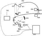
图1是本发明一较佳实施例中超快电子器件响应测试系统的结构示意图;Fig. 1 is the structural representation of ultrafast electronic device response test system in a preferred embodiment of the present invention;
图中各标记的含义是:100-飞秒脉冲激光器、201-分光镜、202-延时线、301-光纤耦合系统光纤、302-无色差光纤、303-超快光电转换器、304-超快光电转换器进行位置操作的控制器、305-光聚光反射镜、401-分光镜、402-光纤耦合系统、403-无色差光纤、404-耦合在光纤头上的电光晶体、405-偏振分光镜、406-光电探测器1、407-光电探测器2、408-光电转换器进行位置操作的控制器、409-聚光反射镜、500-数据采集校正系统。 The meanings of the marks in the figure are: 100-femtosecond pulse laser, 201-beam splitter, 202-delay line, 301-fiber coupling system fiber, 302-chromatic aberration fiber, 303-ultrafast photoelectric converter, 304-ultra Controller for position operation of fast photoelectric converter, 305-light-condensing reflector, 401-beam splitter, 402-fiber coupling system, 403-achromatic fiber, 404-electro-optic crystal coupled to the fiber head, 405-polarization Spectroscope, 406-photodetector 1, 407-photodetector 2, 408-controller for position operation of photoelectric converter, 409-condensing reflector, 500-data acquisition and correction system.
具体实施方式Detailed ways
以下结合附图及一较佳实施例对本发明的技术方案作进一步的说明。The technical solution of the present invention will be further described below in conjunction with the accompanying drawings and a preferred embodiment.
参阅图1,该超快电子器件响应测试系统系采用模块化设计,其包括飞秒脉冲激光器100、飞秒脉冲延时系统、电脉冲产生模块、电脉冲探测模块以及数据采集校正系统500。Referring to FIG. 1 , the ultrafast electronic device response testing system adopts a modular design, which includes a
其中,飞秒脉冲激光器用于提供飞秒光学短脉冲;Among them, the femtosecond pulse laser is used to provide femtosecond optical short pulses;
飞秒脉冲延时系统用于提供测量系统的信号发生和探测的时间延迟变化,它包括201-分光镜、延时线202;The femtosecond pulse delay system is used to provide the time delay change of signal generation and detection of the measurement system, which includes 201-spectroscopic mirror and
电脉冲产生模块用于提供一个产生时间可以控制的测试电脉冲;The electric pulse generating module is used to provide a test electric pulse whose generation time can be controlled;
电脉冲探测模块可以探测在很短时间内(几飞秒到皮秒)的电信号;The electrical pulse detection module can detect electrical signals within a short period of time (femtoseconds to picoseconds);
数据采集校正系统500用于采集光电探测器中的输出信号,解决测量中的本底扣除,时间频率的相互转换。The data collection and
进一步的讲,Further speaking,
前述飞秒脉冲延时系统包括:The aforementioned femtosecond pulse delay system includes:
用于将输入的一束飞秒光学短脉冲分成两束飞秒脉冲光的分光镜201;A beam splitter 201 for splitting an input beam of femtosecond optical short pulse into two beams of femtosecond pulse light;
以及内置反射镜对的延时线202,通过调整所述反射镜对的空间位置可改变脉冲的光程差,进而实现两束飞秒脉冲光的延时。 As well as the
前述电脉冲产生模块包括光纤耦合系统301、无色差光纤302、超快光电转换器303、对超快光电转换器进行位置操作的控制器304以及聚光反射镜305;The aforementioned electrical pulse generation module includes a
聚光反射镜305将飞秒脉冲光聚焦到光纤耦合系统301,然后光纤耦合系统301将飞秒脉冲光耦合入无色差光纤302,无色差光纤302中的脉冲光激发附着在无色差光纤头上的超快光电转换器303发出电信号,控制器304用于将超快光电转换器303放置于被测超快电子器件的输入端。The concentrating
前述超快光电转换器选自转换时间小于30 ps的超快光电二级管、光导天线、TeZn晶体、LiNbO3晶体、LiTaO3晶体、ZnTe晶体、InP晶体和AsGa晶体中的任意一种以上。The aforementioned ultrafast photoelectric converter is selected from any one or more of ultrafast photodiodes, photoconductive antennas, TeZn crystals, LiNbO3 crystals, LiTaO3 crystals, ZnTe crystals, InP crystals, and AsGa crystals with conversion times less than 30 ps.
前述电脉冲探测模块包括分光镜401、光纤耦合系统402、无色差光纤403、耦合在无色差光纤头上的电光晶体404、偏振分光镜405、第一光电探测器406、第二光电探测器407、对光电转换器进行位置操作的控制器408以及聚光反射镜409;The aforementioned electrical pulse detection module includes a
聚光反射镜409将飞秒脉冲光聚焦到光纤耦合系统402后,由光纤耦合系统402将脉冲光耦合入无色差光纤403,再由所述电光晶体404反射入无色差光纤403,并从光纤耦合系统402出射,其后通过分光镜401反射入偏振分光镜405形成两束正交偏振的光,而后分别由第一光电探测器406、和第二光电探测器407对该两束正交偏振的光的光强变化进行测量;After the
所述控制器408用于将所述电光晶体404放置于被测超快电子器件的输出端。The
前述电光晶体选自ZnTe晶体、InP晶体和AsGa晶体中的任意一种以上。The aforementioned electro-optic crystal is selected from any one or more of ZnTe crystal, InP crystal and AsGa crystal.
本实施例中,由飞秒脉冲激光器产生的飞秒光学短脉冲被输入飞秒脉冲延时系统后,被分光镜201分为两束,这两束光的光程差可以由调节延时线202中的反光镜对的空间位置来控制,实现两束飞秒脉冲光的延时,其中一束脉冲光进入电脉冲产生模块,在该模块中,聚光镜305将脉冲光聚焦到光纤耦合系统301中,然后用光纤耦合系统将脉冲光耦合到无色差光纤302中,激光脉冲激发附着在光纤头上的超快光电转换器303发出电信号,该电信号输入被测电子器件中,电子器件的输出信号改变电光晶体404的瞬间折射率比,从而改变入射的脉冲光的极化方向。在电脉冲探测模块中,由聚光镜409将飞秒激光束聚焦到光纤耦合系统402,耦合入无色差光纤403的飞秒激光脉冲在电光晶体404中反射回来,通过光纤耦合系统后经由分光镜401进入偏振分光镜405,并在偏振分光镜中被分为不同偏振的两束,通过两个光电探测器406和光电探测407分别测量这两束光的光强的相对强弱,可以计算出激光脉冲到达是电光晶体上的电场强度。In this embodiment, after the femtosecond optical short pulse produced by the femtosecond pulse laser is input into the femtosecond pulse delay system, it is divided into two beams by the
通过改变前述两束飞秒脉冲光的延迟时间,就可以得到电光晶体上的电场的时序变化。By changing the delay time of the aforementioned two beams of femtosecond pulsed light, the temporal variation of the electric field on the electro-optic crystal can be obtained.
需要说明的是,本实施例的测试系统中在没有被测器件时,电场变化可能有一定的延长和改变,但可以通过测量没有被测器件时的时序变化曲线来矫正测量结果。It should be noted that in the test system of this embodiment, when there is no device under test, the electric field change may be extended and changed to a certain extent, but the measurement results can be corrected by measuring the time series change curve without the device under test.
通过分析有被测器件和无被测器件两种情况下的时序曲线的区别,就可以获取被测超快电子器件的时间和频率响应的性质。By analyzing the difference between the timing curves with and without the device under test, the properties of the time and frequency response of the ultrafast electronic device under test can be obtained.
本发明可实现对超快电子器件的时间和频率响应性质的同步评测,并可克服现有电子学测量中时间分辨率不足的缺陷。The invention can realize the synchronous evaluation of the time and frequency response properties of ultra-fast electronic devices, and can overcome the defect of insufficient time resolution in the existing electronic measurement.
上述较佳实施例只为说明本发明的技术构思及特点,其目的在于让熟悉此项技术的认识能够了解本发明的内容并据以实施,并不能以此限制本发明的保护范围,凡根据本发明精神实质所作的等效变化或者修饰,都应涵盖在本发明的保护范围之内。The above-mentioned preferred embodiments are only to illustrate the technical conception and characteristics of the present invention, and its purpose is to allow those who are familiar with this technology to understand the content of the present invention and implement it accordingly, and cannot limit the protection scope of the present invention with this. Equivalent changes or modifications made to the spirit of the present invention shall fall within the protection scope of the present invention.
Claims (10)
Translated fromChinesePriority Applications (1)
| Application Number | Priority Date | Filing Date | Title |
|---|---|---|---|
| CN 201110269306CN102426306B (en) | 2011-09-13 | 2011-09-13 | Ultrafast electronic device testing system and method |
Applications Claiming Priority (1)
| Application Number | Priority Date | Filing Date | Title |
|---|---|---|---|
| CN 201110269306CN102426306B (en) | 2011-09-13 | 2011-09-13 | Ultrafast electronic device testing system and method |
Publications (2)
| Publication Number | Publication Date |
|---|---|
| CN102426306Atrue CN102426306A (en) | 2012-04-25 |
| CN102426306B CN102426306B (en) | 2013-06-26 |
Family
ID=45960311
Family Applications (1)
| Application Number | Title | Priority Date | Filing Date |
|---|---|---|---|
| CN 201110269306Expired - Fee RelatedCN102426306B (en) | 2011-09-13 | 2011-09-13 | Ultrafast electronic device testing system and method |
Country Status (1)
| Country | Link |
|---|---|
| CN (1) | CN102426306B (en) |
Cited By (4)
| Publication number | Priority date | Publication date | Assignee | Title |
|---|---|---|---|---|
| CN106353634A (en)* | 2016-10-17 | 2017-01-25 | 深圳市太赫兹科技创新研究院 | Terahertz time-domain reflecting system |
| CN112858805A (en)* | 2020-12-29 | 2021-05-28 | 西南技术物理研究所 | Frequency response characteristic parameter measuring device for quadrant photoelectric detector |
| CN113203761A (en)* | 2021-04-21 | 2021-08-03 | 华中科技大学 | Time resolution sample inspection device with multiple working modes |
| CN114459621A (en)* | 2022-02-10 | 2022-05-10 | 中国空间技术研究院 | Superconducting X-ray detector time jitter calibration system and method |
Citations (3)
| Publication number | Priority date | Publication date | Assignee | Title |
|---|---|---|---|---|
| US4931704A (en)* | 1988-12-09 | 1990-06-05 | Alfano Robert R | Ultrafast sampling oscilloscope |
| JPH05126866A (en)* | 1991-11-05 | 1993-05-21 | Nippon Steel Corp | Ultra-high-speed electrical signal measuring method and apparatus |
| US20020097761A1 (en)* | 1994-04-01 | 2002-07-25 | Imra America, Inc. | Scanning temporal ultrafast delay methods and apparatuses therefor |
- 2011
- 2011-09-13CNCN 201110269306patent/CN102426306B/ennot_activeExpired - Fee Related
Patent Citations (4)
| Publication number | Priority date | Publication date | Assignee | Title |
|---|---|---|---|---|
| US4931704A (en)* | 1988-12-09 | 1990-06-05 | Alfano Robert R | Ultrafast sampling oscilloscope |
| JPH05126866A (en)* | 1991-11-05 | 1993-05-21 | Nippon Steel Corp | Ultra-high-speed electrical signal measuring method and apparatus |
| US20020097761A1 (en)* | 1994-04-01 | 2002-07-25 | Imra America, Inc. | Scanning temporal ultrafast delay methods and apparatuses therefor |
| EP0790492B1 (en)* | 1996-02-16 | 2005-12-28 | Imra America, Inc. | Scanning temporal ultrafast delay method |
Cited By (7)
| Publication number | Priority date | Publication date | Assignee | Title |
|---|---|---|---|---|
| CN106353634A (en)* | 2016-10-17 | 2017-01-25 | 深圳市太赫兹科技创新研究院 | Terahertz time-domain reflecting system |
| WO2018072660A1 (en)* | 2016-10-17 | 2018-04-26 | 深圳市太赫兹科技创新研究院 | Terahertz time-domain reflectometry system |
| CN112858805A (en)* | 2020-12-29 | 2021-05-28 | 西南技术物理研究所 | Frequency response characteristic parameter measuring device for quadrant photoelectric detector |
| CN112858805B (en)* | 2020-12-29 | 2023-02-28 | 西南技术物理研究所 | Frequency response characteristic parameter measuring device for quadrant photoelectric detector |
| CN113203761A (en)* | 2021-04-21 | 2021-08-03 | 华中科技大学 | Time resolution sample inspection device with multiple working modes |
| CN113203761B (en)* | 2021-04-21 | 2022-04-01 | 华中科技大学 | Time resolution sample inspection device with multiple working modes |
| CN114459621A (en)* | 2022-02-10 | 2022-05-10 | 中国空间技术研究院 | Superconducting X-ray detector time jitter calibration system and method |
Also Published As
| Publication number | Publication date |
|---|---|
| CN102426306B (en) | 2013-06-26 |
Similar Documents
| Publication | Publication Date | Title |
|---|---|---|
| CN103712689B (en) | Continuous laser device spectral line width measurement device based on optical frequency comb | |
| WO2018072660A1 (en) | Terahertz time-domain reflectometry system | |
| CN101900608B (en) | Multifunctional wide-range ultra-short pulsed laser autocorrelator | |
| CN102620666A (en) | Detecting system for semiconductor wafer thickness and detecting method thereof | |
| CN105548722B (en) | A kind of measuring system of ferromagnetic material Terahertz dielectric constant | |
| CN110567595A (en) | A method and system for real-time measurement of transient ultrashort pulse time width | |
| CN102426306B (en) | Ultrafast electronic device testing system and method | |
| CN102768184A (en) | System for Young modulus measurement of film | |
| CN103048053A (en) | Single laser signal-to-noise ratio detection device | |
| CN109060150B (en) | Ultra-short pulse time width measuring device and method based on spectral interference | |
| CN103776550B (en) | Based on super continuous spectrums pulse laser measurement mechanism and the method for non-linear nano material | |
| CN103903967B (en) | A kind of laser anneal device and method | |
| CN101793916A (en) | All-fiber current monitoring device based on Faraday effect | |
| CN110823388A (en) | Film thermal response single-pulse detection method under ultrafast laser photon time stretching | |
| CN103471815B (en) | Method for simultaneously measuring reflectivity of S and P polarized light of high-reflection mirror | |
| CN106895911A (en) | A kind of high-rate laser power measurement instruments | |
| CN103454074A (en) | Method for measuring reflectivity of small-aperture high-reflectivity mirror | |
| CN202511762U (en) | Semiconductor wafer thickness detection system | |
| CN107478604B (en) | Device and method for measuring refractive index of transparent material | |
| CN105699980A (en) | High-precision laser range unit and measurement method | |
| CN204461621U (en) | Ultrafast pulse waveform time domain measuring system | |
| CN107560726B (en) | Arc sensor and arc detection method | |
| CN106959166A (en) | The measurement apparatus and method of any repetition rate femtosecond laser time jitter | |
| CN104459594B (en) | A kind of measurement apparatus of high-frequency microwave probe multifrequency characteristic and method | |
| JP2010093243A (en) | Optical peak power detection apparatus, and pulse laser generation apparatus using the same |
Legal Events
| Date | Code | Title | Description |
|---|---|---|---|
| C06 | Publication | ||
| PB01 | Publication | ||
| C10 | Entry into substantive examination | ||
| SE01 | Entry into force of request for substantive examination | ||
| C14 | Grant of patent or utility model | ||
| GR01 | Patent grant | ||
| CF01 | Termination of patent right due to non-payment of annual fee | Granted publication date:20130626 Termination date:20200913 | |
| CF01 | Termination of patent right due to non-payment of annual fee |