CN102422210A - Liquid crystal display device - Google Patents
Liquid crystal display deviceDownload PDFInfo
- Publication number
- CN102422210A CN102422210ACN2010800205209ACN201080020520ACN102422210ACN 102422210 ACN102422210 ACN 102422210ACN 2010800205209 ACN2010800205209 ACN 2010800205209ACN 201080020520 ACN201080020520 ACN 201080020520ACN 102422210 ACN102422210 ACN 102422210A
- Authority
- CN
- China
- Prior art keywords
- liquid crystal
- display device
- crystal display
- bus line
- substrate
- Prior art date
- Legal status (The legal status is an assumption and is not a legal conclusion. Google has not performed a legal analysis and makes no representation as to the accuracy of the status listed.)
- Pending
Links
Images


Classifications
- G—PHYSICS
- G02—OPTICS
- G02F—OPTICAL DEVICES OR ARRANGEMENTS FOR THE CONTROL OF LIGHT BY MODIFICATION OF THE OPTICAL PROPERTIES OF THE MEDIA OF THE ELEMENTS INVOLVED THEREIN; NON-LINEAR OPTICS; FREQUENCY-CHANGING OF LIGHT; OPTICAL LOGIC ELEMENTS; OPTICAL ANALOGUE/DIGITAL CONVERTERS
- G02F1/00—Devices or arrangements for the control of the intensity, colour, phase, polarisation or direction of light arriving from an independent light source, e.g. switching, gating or modulating; Non-linear optics
- G02F1/01—Devices or arrangements for the control of the intensity, colour, phase, polarisation or direction of light arriving from an independent light source, e.g. switching, gating or modulating; Non-linear optics for the control of the intensity, phase, polarisation or colour
- G02F1/13—Devices or arrangements for the control of the intensity, colour, phase, polarisation or direction of light arriving from an independent light source, e.g. switching, gating or modulating; Non-linear optics for the control of the intensity, phase, polarisation or colour based on liquid crystals, e.g. single liquid crystal display cells
- G02F1/133—Constructional arrangements; Operation of liquid crystal cells; Circuit arrangements
- G02F1/1333—Constructional arrangements; Manufacturing methods
- G02F1/1343—Electrodes
- G02F1/134309—Electrodes characterised by their geometrical arrangement
- G02F1/134363—Electrodes characterised by their geometrical arrangement for applying an electric field parallel to the substrate, i.e. in-plane switching [IPS]
- G—PHYSICS
- G02—OPTICS
- G02F—OPTICAL DEVICES OR ARRANGEMENTS FOR THE CONTROL OF LIGHT BY MODIFICATION OF THE OPTICAL PROPERTIES OF THE MEDIA OF THE ELEMENTS INVOLVED THEREIN; NON-LINEAR OPTICS; FREQUENCY-CHANGING OF LIGHT; OPTICAL LOGIC ELEMENTS; OPTICAL ANALOGUE/DIGITAL CONVERTERS
- G02F1/00—Devices or arrangements for the control of the intensity, colour, phase, polarisation or direction of light arriving from an independent light source, e.g. switching, gating or modulating; Non-linear optics
- G02F1/01—Devices or arrangements for the control of the intensity, colour, phase, polarisation or direction of light arriving from an independent light source, e.g. switching, gating or modulating; Non-linear optics for the control of the intensity, phase, polarisation or colour
- G02F1/13—Devices or arrangements for the control of the intensity, colour, phase, polarisation or direction of light arriving from an independent light source, e.g. switching, gating or modulating; Non-linear optics for the control of the intensity, phase, polarisation or colour based on liquid crystals, e.g. single liquid crystal display cells
- G02F1/133—Constructional arrangements; Operation of liquid crystal cells; Circuit arrangements
- G02F1/1333—Constructional arrangements; Manufacturing methods
- G02F1/1345—Conductors connecting electrodes to cell terminals
- G—PHYSICS
- G02—OPTICS
- G02F—OPTICAL DEVICES OR ARRANGEMENTS FOR THE CONTROL OF LIGHT BY MODIFICATION OF THE OPTICAL PROPERTIES OF THE MEDIA OF THE ELEMENTS INVOLVED THEREIN; NON-LINEAR OPTICS; FREQUENCY-CHANGING OF LIGHT; OPTICAL LOGIC ELEMENTS; OPTICAL ANALOGUE/DIGITAL CONVERTERS
- G02F1/00—Devices or arrangements for the control of the intensity, colour, phase, polarisation or direction of light arriving from an independent light source, e.g. switching, gating or modulating; Non-linear optics
- G02F1/01—Devices or arrangements for the control of the intensity, colour, phase, polarisation or direction of light arriving from an independent light source, e.g. switching, gating or modulating; Non-linear optics for the control of the intensity, phase, polarisation or colour
- G02F1/13—Devices or arrangements for the control of the intensity, colour, phase, polarisation or direction of light arriving from an independent light source, e.g. switching, gating or modulating; Non-linear optics for the control of the intensity, phase, polarisation or colour based on liquid crystals, e.g. single liquid crystal display cells
- G02F1/133—Constructional arrangements; Operation of liquid crystal cells; Circuit arrangements
- G02F1/1333—Constructional arrangements; Manufacturing methods
- G02F1/1337—Surface-induced orientation of the liquid crystal molecules, e.g. by alignment layers
- G02F1/133742—Surface-induced orientation of the liquid crystal molecules, e.g. by alignment layers for homeotropic alignment
- G—PHYSICS
- G02—OPTICS
- G02F—OPTICAL DEVICES OR ARRANGEMENTS FOR THE CONTROL OF LIGHT BY MODIFICATION OF THE OPTICAL PROPERTIES OF THE MEDIA OF THE ELEMENTS INVOLVED THEREIN; NON-LINEAR OPTICS; FREQUENCY-CHANGING OF LIGHT; OPTICAL LOGIC ELEMENTS; OPTICAL ANALOGUE/DIGITAL CONVERTERS
- G02F1/00—Devices or arrangements for the control of the intensity, colour, phase, polarisation or direction of light arriving from an independent light source, e.g. switching, gating or modulating; Non-linear optics
- G02F1/01—Devices or arrangements for the control of the intensity, colour, phase, polarisation or direction of light arriving from an independent light source, e.g. switching, gating or modulating; Non-linear optics for the control of the intensity, phase, polarisation or colour
- G02F1/13—Devices or arrangements for the control of the intensity, colour, phase, polarisation or direction of light arriving from an independent light source, e.g. switching, gating or modulating; Non-linear optics for the control of the intensity, phase, polarisation or colour based on liquid crystals, e.g. single liquid crystal display cells
- G02F1/133—Constructional arrangements; Operation of liquid crystal cells; Circuit arrangements
- G02F1/136—Liquid crystal cells structurally associated with a semi-conducting layer or substrate, e.g. cells forming part of an integrated circuit
- G02F1/13606—Liquid crystal cells structurally associated with a semi-conducting layer or substrate, e.g. cells forming part of an integrated circuit having means for reducing parasitic capacitance
Landscapes
- Physics & Mathematics (AREA)
- Nonlinear Science (AREA)
- Mathematical Physics (AREA)
- Chemical & Material Sciences (AREA)
- Crystallography & Structural Chemistry (AREA)
- General Physics & Mathematics (AREA)
- Optics & Photonics (AREA)
- Geometry (AREA)
- Liquid Crystal (AREA)
Abstract
Description
Translated fromChinese技术领域technical field
本发明涉及液晶显示装置。详细地说,涉及适合有源矩阵型液晶显示装置的液晶显示装置。The present invention relates to a liquid crystal display device. Specifically, it relates to a liquid crystal display device suitable for an active matrix type liquid crystal display device.
背景技术Background technique
使用以薄膜晶体管(TFT)为代表的有源元件的有源矩阵型液晶显示装置,由于其具有薄型、轻量的特征和匹敌阴极射线管(Braun tube)的高画质,作为显示装置被广泛普及。Active-matrix liquid crystal display devices using active elements represented by thin-film transistors (TFTs) are widely used as display devices due to their thin and lightweight features and high image quality comparable to cathode ray tubes (Braun tubes). universal.
该有源矩阵型液晶显示装置的显示方式中,公知大致区分为以下两种显示方式。Among the display methods of this active matrix type liquid crystal display device, the following two display methods are generally known.
一种方式是,在分别形成有透明电极的一对基板之间封入液晶层,通过对2个透明电极施加驱动电压,由在基板界面的大致直角方向的电场驱动液晶层,调制透过一个透明电极射入液晶层的光进行显示的方式(以下,称作纵向电场方式)。One method is to seal a liquid crystal layer between a pair of substrates respectively formed with transparent electrodes, and by applying a driving voltage to the two transparent electrodes, the liquid crystal layer is driven by an electric field in a direction approximately at right angles to the interface of the substrates, modulating a transparent A method of displaying light incident on the liquid crystal layer through the electrodes (hereinafter referred to as a vertical electric field method).
然而,在采用纵向电场方式的有源矩阵型液晶显示装置中,使视角方向变化时的亮度变化大,特别是,在进行中间灰度显示的情况下,有可能由于视角方向导致灰度等级水平反转。However, in an active matrix liquid crystal display device using a vertical electric field method, the luminance changes greatly when the viewing angle direction is changed. reverse.
另外,另一种方式是,在一对基板之间封入液晶层,通过向在同一基板或者在两个基板上形成的2个电极施加驱动电压,由在基板界面大致平行方向的电场驱动液晶层,调制从2个电极的间隙入射的光进行显示的方式(以下,称作横向电场方式)。In another method, a liquid crystal layer is sealed between a pair of substrates, and a driving voltage is applied to two electrodes formed on the same substrate or two substrates, and the liquid crystal layer is driven by an electric field approximately parallel to the substrate interface. , a method of modulating light incident from a gap between two electrodes to perform display (hereinafter referred to as a transverse electric field method).
作为横向电场方式的液晶模式,公知的有IPS(In-plane Switching:平面转换)模式、TBA(Transverse Bend Alignment:横向弯曲对准)模式等。As the liquid crystal mode of the transverse electric field method, IPS (In-plane Switching: in-plane switching) mode, TBA (Transverse Bend Alignment: transverse bend alignment) mode, etc. are known.
在任何一种的模式中,都利用由连接有TFT等的有源元件的像素电极,和作为在各像素中共用的电极的共用电极产生的横向电场来驱动液晶层。In either mode, the liquid crystal layer is driven by a lateral electric field generated by a pixel electrode to which an active element such as a TFT is connected, and a common electrode which is an electrode common to each pixel.
作为IPS模式的液晶显示装置,例如公开有:在采用横向电场方式的有源矩阵型液晶显示装置中,作为提高对比度并且防止产生亮度不均的技术,像素电极和共用电极的至少一方的电极的侧面与基板面所成的角超过0°不足90°的液晶显示装置(例如,参照专利文献1)。As an IPS mode liquid crystal display device, for example, in an active matrix type liquid crystal display device adopting a transverse electric field method, as a technique for improving contrast and preventing occurrence of brightness unevenness, an electrode of at least one of a pixel electrode and a common electrode is disclosed. A liquid crystal display device in which the angle formed between the side surface and the substrate surface exceeds 0° and is less than 90° (for example, refer to Patent Document 1).
另外,TBA模式是作为液晶材料使用p型向列型液晶,通过由横向电场驱动该液晶来规定液晶分子的取向方位的显示方式。按照TBA模式,能够保持由垂直取向产生的高对比性。In the TBA mode, a p-type nematic liquid crystal is used as a liquid crystal material, and the liquid crystal is driven by a transverse electric field to define the orientation of liquid crystal molecules. According to the TBA mode, it is possible to maintain the high contrast resulting from the vertical orientation.
现有技术文献prior art literature
专利文献patent documents
专利文献1:日本特平9-90410号公报Patent Document 1: Japanese Patent Application Publication No. 9-90410
发明内容Contents of the invention
发明要解决的课题The problem to be solved by the invention
以下,以上述的横向电场方式的液晶显示装置为例,说明本发明的课题和达成本发明的经过,其中,本发明的液晶显示装置不限定于上述的横向电场方式的液晶显示装置。Hereinafter, the subject of the present invention and the process of achieving the present invention will be described by taking the above-mentioned transverse electric field liquid crystal display device as an example. The liquid crystal display device of the present invention is not limited to the above-mentioned transverse electric field liquid crystal display device.
在现有技术中的横向电场方式的液晶显示装置中,存在在施加于共用电极的共用信号中产生噪音,显示品质降低降低的情况。具体来说,存在画面闪烁或者产生暗的部分(阴影)的情况。In a conventional transverse electric field type liquid crystal display device, noise may be generated in a common signal applied to a common electrode, and display quality may deteriorate. Specifically, there are cases where the screen flickers or dark parts (shadows) are generated.
另外,该现象在像素为高精细的情况下特别显著地产生。另外一般来说,像素越是高精细各配线的宽度越细,并且像素数量越多。因此,认为该现象的产生是由于作为附加的电容的附加电容增大,其结果是,在共用信号中产生噪音所致。In addition, this phenomenon occurs particularly remarkably in the case of high-definition pixels. In general, the finer the pixels, the thinner the width of each wiring, and the larger the number of pixels. Therefore, it is considered that this phenomenon occurs because the additional capacitance, which is an additional capacitance, increases, and as a result, noise is generated in the common signal.
本发明,是鉴于上述现状而完成的,其目的为:提供能够抑制由附加电容引起的显示品质的降低的液晶显示装置。The present invention has been made in view of the above-mentioned circumstances, and an object of the present invention is to provide a liquid crystal display device capable of suppressing a decrease in display quality due to additional capacitance.
课题解决的手段means of problem solving
本发明者们,在对能够抑制由附加电容导致的显示品质的降低的液晶显示装置作各种研讨时,关注向共用电极的共用信号的输入(施加)方法。于是发现:在现有技术中,例如在专利文献1中记载的技术中,在显示区域中,由于共用电极与栅极总线或源极总线配置在相同的层,栅极总线或源极总线发生故障,因为只能够从显示区域的上下或左右向共用电极输入共用信号,因此,如上所述附加电容增大。The inventors of the present invention paid attention to a method of inputting (applying) a common signal to a common electrode while conducting various studies on a liquid crystal display device capable of suppressing a decrease in display quality due to an additional capacitance. Then it was found that in the prior art, such as the technology described in Patent Document 1, in the display area, since the common electrode is arranged on the same layer as the gate bus line or the source bus line, the gate bus line or the source bus line occurs The fault is that the common signal can only be input to the common electrode from the top, bottom or left and right of the display area, so the additional capacitance increases as described above.
并且,进一步研讨后发现:在显示区域中,通过将共用电极配置在与形成有栅极总线的层和形成有源极总线的层不同的层,能够不影响栅极总线和源极总线地更加自由地设计共用电极的布局,因此,能够从比现有技术更多的方向向显示区域输入共用信号,其结果,能够抑制附加电容,并想到能够很好地解决上述课题的方法,实现本发明。Furthermore, after further study, it was found that, in the display region, by arranging the common electrode in a layer different from the layer on which the gate bus line and the layer on which the source bus line are formed, it is possible to achieve a more stable performance without affecting the gate bus line and the source bus line. The layout of the common electrodes can be freely designed, therefore, the common signal can be input to the display area from more directions than in the prior art, and as a result, the additional capacitance can be suppressed, and a method that can solve the above-mentioned problems well has been conceived, and the present invention has been realized. .
即,本发明是一种液晶显示装置,其具备:相互相对配置的第一基板和第二基板;和被夹持在上述第一基板与上述第二基板之间的液晶层,其中,上述第一基板具有栅极总线、源极总线、被输入图像信号的像素电极和被输入共用信号的共用电极,上述像素电极和上述共用电极在像素内为梳齿状,在像素内在上述像素电极和上述共用电极之间,产生平行于上述第一基板面的电场,上述共用电极配置在显示区域中的与形成有上述栅极总线的层和形成有上述源极总线的层不同的层。That is, the present invention is a liquid crystal display device comprising: a first substrate and a second substrate arranged to face each other; and a liquid crystal layer sandwiched between the first substrate and the second substrate, wherein the first A substrate has a gate bus line, a source bus line, a pixel electrode to which an image signal is input, and a common electrode to which a common signal is input. The pixel electrode and the common electrode are comb-shaped in the pixel. An electric field parallel to the first substrate surface is generated between the common electrodes, and the common electrodes are arranged in a layer different from the layer in which the gate bus lines are formed and the layer in which the source bus lines are formed in the display region.
并且,“产生平行于上述第一基板面的电场”表示“至少产生具有平行于上述第1基板面的成分的电场”。即,上述“平行”包括“大致平行”和“倾斜”。Also, "generating an electric field parallel to the first substrate surface" means "generating an electric field having at least a component parallel to the first substrate surface". That is, the above-mentioned "parallel" includes "substantially parallel" and "oblique".
作为本发明的液晶显示装置的结构,只要将这样的构成要素作为必须要素而形成,对于其它的构成要素没有作特别地限定。对本发明的液晶显示装置的优选方式在下文进行详细地说明。并且,以下所示的各方式可以适当地组合。The configuration of the liquid crystal display device of the present invention is not particularly limited to other constituent elements as long as such constituent elements are formed as essential elements. Preferred embodiments of the liquid crystal display device of the present invention will be described in detail below. In addition, each aspect shown below can be combined suitably.
优选上述共用信号,沿着上述栅极总线和上述源极总线(更加优选的是,上述栅极总线和上述源极总线的在显示区域的延伸方向),从至少3个方向被输入到显示区域中。由此,能够更加可靠地抑制附加电容。Preferably, the common signal is input to the display region from at least three directions along the gate bus line and the source bus line (more preferably, the direction in which the gate bus line and the source bus line extend in the display region). middle. Thereby, additional capacitance can be suppressed more reliably.
优选上述共用信号,沿着上述栅极总线和上述源极总线(更加优选的是,上述栅极总线和上述源极总线的在显示区域中的延伸方向),从4个方向被输入到显示区域内。由此,因为能够更加可靠地抑制附加电容,所以能够进一步抑制显示品质的降低。Preferably, the common signal is input to the display area from four directions along the gate bus line and the source bus line (more preferably, the direction in which the gate bus line and the source bus line extend in the display area). Inside. As a result, since the additional capacitance can be suppressed more reliably, it is possible to further suppress a decrease in display quality.
更加具体地说,优选上述显示区域在俯视时为矩形状,上述共用信号从显示区域的至少3边被输入到显示区域内。由此,能够从至少3个方向向俯视时为矩形状的显示区域内可靠地输入共用信号。More specifically, it is preferable that the display area is rectangular in plan view, and that the common signal is input into the display area from at least three sides of the display area. Thereby, the common signal can be reliably input from at least three directions in the rectangular-shaped display area in planar view.
另外,这时,优选上述共用信号从显示区域的4边被输入到显示区域中。由此,能够从4个方向向俯视时为矩形状的显示区域内可靠地输入共用信号。In addition, at this time, it is preferable that the above-mentioned common signal is input into the display area from four sides of the display area. Thereby, the common signal can be reliably input from four directions in the rectangular display area in planar view.
优选上述共用电极在显示区域外与上述栅极总线和上述源极总线交叉。由此,能够以包围显示区域的外周的方式配置共用电极。因此,能够从至少3个方向向显示区域内有效地输入共用信号。Preferably, the common electrode intersects the gate bus lines and the source bus lines outside the display area. Thereby, the common electrode can be arranged so as to surround the outer periphery of the display region. Therefore, a common signal can be effectively input into the display area from at least three directions.
优选上述共用电极包围显示区域的全部外周。由此,能够从4个方向向显示区域内有效地输入共用信号。Preferably, the common electrode surrounds the entire periphery of the display region. Thereby, the common signal can be effectively input into the display area from four directions.
优选上述共用电极包括:沿着相邻的像素之间的边界形成的边界部(共用边界部);和从上述边界部延伸到像素内的分支部(共用分支部)。Preferably, the common electrode includes: a boundary portion (common boundary portion) formed along a boundary between adjacent pixels; and a branch portion (common branch portion) extending from the boundary portion into the pixel.
优选上述边界部覆盖上述栅极总线和上述源极总线。由此,因为能够遮蔽由栅极总线和源极总线所引起的电场,所以能够抑制发生由该电场引起的液晶取向不良,即抑制在像素内产生不良畴。Preferably, the boundary portion covers the gate bus line and the source bus line. As a result, since the electric field caused by the gate bus line and the source bus line can be shielded, occurrence of liquid crystal misalignment caused by the electric field, that is, occurrence of defective domains in the pixel can be suppressed.
优选上述共用电极和像素电极,在显示区域内被配置在相同层。由此,能够实现制造工序的简化。Preferably, the common electrode and the pixel electrode are arranged in the same layer in the display region. This enables simplification of the manufacturing process.
优选上述第一基板还具有保持电容配线,上述保持电容配线,在显示区域中被配置在与形成有上述共用电极的层不同的层。由此,能够不对共用电极的布局造成影响地形成保持电容配线。Preferably, the first substrate further includes storage capacitor wiring, and the storage capacitor wiring is arranged in a layer different from the layer in which the common electrode is formed in the display region. Accordingly, storage capacitor wiring can be formed without affecting the layout of the common electrode.
优选向上述保持电容配线输入与上述共用信号相同的信号。由此,能够实现成本消减。Preferably, the same signal as the common signal is input to the holding capacitor wiring. Thereby, cost reduction can be achieved.
优选上述保持电容配线与上述共用电极连接。由此,能够向保持电容配线有效地输入与共用信号相同的信号。Preferably, the storage capacitor wiring is connected to the common electrode. Accordingly, the same signal as the common signal can be efficiently input to the storage capacitor wiring.
优选上述保持电容配线在显示区域外与上述共用电极连接。由此,因为变得可以不在显示区域(像素)内形成用于连接保持电容配线和共用电极的接触孔,所以能够提高像素的开口率,提高透过率。Preferably, the storage capacitor wiring is connected to the common electrode outside the display area. This eliminates the need to form a contact hole for connecting the storage capacitor wiring and the common electrode in the display region (pixel), so that the aperture ratio of the pixel can be increased and the transmittance can be improved.
优选上述第一基板,还具有在显示区域外形成的Cs连接配线,优选上述Cs连接配线与上述保持电容配线的一端连接。由此,能够从保持电容配线的两端输入信号。Preferably, the first substrate further includes a Cs connection line formed outside the display area, and it is preferable that the Cs connection line is connected to one end of the storage capacitor line. Thus, signals can be input from both ends of the storage capacitor wiring.
优选上述Cs连接配线,在显示区域外与上述共用电极连接。由此,因为没必要在显示区域(像素)内形成用于连接保持电容配线和共用电极的接触孔,所以能够在显示区域外通过Cs连接配线连接保持电容配线和共用电极。Preferably, the Cs connection wiring is connected to the common electrode outside the display area. Accordingly, since there is no need to form a contact hole for connecting the storage capacitor line and the common electrode in the display area (pixel), the storage capacitor line and the common electrode can be connected through the Cs connection line outside the display area.
优选上述共用电极,在显示区域中配置在比上述栅极总线和上述源极总线更靠上述液晶层一侧。由此,能够更加有效地产生平行于液晶层的电场。Preferably, the common electrode is arranged on a side closer to the liquid crystal layer than the gate bus lines and the source bus lines in the display region. Accordingly, an electric field parallel to the liquid crystal layer can be more efficiently generated.
另外,这时,优选上述第一基板还具有在上述共用电极与上述栅极总线或上述源极总线的层之间设置的层间绝缘膜,上述层间绝缘膜含有绝缘性树脂模。由此,作为绝缘性树脂膜因为能够使用相对介电常数低的膜,所以能够抑制信号延迟的发生。In this case, it is preferable that the first substrate further includes an interlayer insulating film provided between the common electrode and the gate bus line or the layer of the source bus line, and the interlayer insulating film includes an insulating resin mold. Accordingly, since a film having a low relative permittivity can be used as the insulating resin film, the occurrence of signal delay can be suppressed.
优选上述绝缘性树脂膜含有丙烯酸树脂。由此,能够有效地减小绝缘性树脂膜的相对介电常数。Preferably, the insulating resin film contains an acrylic resin. Accordingly, the relative permittivity of the insulating resin film can be effectively reduced.
优选上述绝缘性树脂膜具有感光性。由此,能够使用于连接共用电极和下层的配线层的接触孔的形成工序简化。It is preferable that the above-mentioned insulating resin film has photosensitivity. Thereby, the formation process of the contact hole for connecting the common electrode and the wiring layer of a lower layer can be simplified.
优选上述绝缘性树脂膜的相对介电常数为2.7~4.5(更加优选的是3.4~3.8)。The relative dielectric constant of the insulating resin film is preferably 2.7 to 4.5 (more preferably 3.4 to 3.8).
上述液晶层,更加具体地说,优选含有p型向列型液晶。More specifically, the liquid crystal layer preferably contains p-type nematic liquid crystal.
上述p型向列型液晶,在未施加电压时,可以相对于上述第一基板和上述第二基板面垂直地取向,在未施加电压时,也可以相对于上述第一基板和上述第二基板面水平地取向。按照前者,能够实现起到本发明的效果的TBA模式的液晶显示装置,按照后者,能够实现起到本发明的效果的IPS模式的液晶显示装置。The p-type nematic liquid crystal can be vertically aligned with respect to the first substrate and the second substrate when no voltage is applied, and can also be aligned with respect to the first substrate and the second substrate when no voltage is applied. oriented horizontally. According to the former, it is possible to realize a TBA mode liquid crystal display device which can achieve the effect of the present invention, and according to the latter, it is possible to realize an IPS mode liquid crystal display device which can achieve the effect of the present invention.
并且,“上述p型向列型液晶相对于上述第一基板和上述第二基板面垂直地或水平地取向”,表示“上述p型向列型液晶,至少具有相对于上述第一基板和上述第二基板面垂直或水平的成分”。即,上述“垂直”也包括“大致垂直”,上述“水平”也包括“大致水平”。And, "the above-mentioned p-type nematic liquid crystal is aligned vertically or horizontally with respect to the above-mentioned first substrate and the above-mentioned second substrate", means "the above-mentioned p-type nematic liquid crystal has at least Vertical or horizontal composition of the second substrate plane". That is, the above-mentioned "vertical" also includes "approximately vertical", and the above-mentioned "horizontal" also includes "approximately horizontal".
发明的效果The effect of the invention
按照本发明的液晶显示装置,能够抑制由附加电容引起的显示品质的降低。According to the liquid crystal display device of the present invention, it is possible to suppress a decrease in display quality due to additional capacitance.
附图说明Description of drawings
图1是表示实施方式1的液晶显示装置的结构的平面图。FIG. 1 is a plan view showing the configuration of a liquid crystal display device according to Embodiment 1. As shown in FIG.
图2(a)是表示实施方式1的液晶显示装置的图像元素的结构的平面示意图,(b)是表示实施方式1的液晶显示装置的偏光板的透过轴的配置关系的概念图。2( a ) is a schematic plan view showing the configuration of picture elements in the liquid crystal display device of Embodiment 1, and (b) is a conceptual diagram showing the arrangement relationship of transmission axes of polarizers in the liquid crystal display device of Embodiment 1.
图3是表示实施方式1的液晶显示装置的结构的截面图,表示图2(a)中的X-Y线的截面。3 is a cross-sectional view showing the structure of the liquid crystal display device according to Embodiment 1, showing a cross-section along line X-Y in FIG. 2( a ).
图4是表示实施方式1的液晶显示装置的结构的截面图,表示施加电压时的液晶的取向分布。4 is a cross-sectional view showing the structure of the liquid crystal display device according to Embodiment 1, showing the orientation distribution of liquid crystals when a voltage is applied.
图5是表示实施方式2的液晶显示装置的结构的截面图。5 is a cross-sectional view showing the configuration of a liquid crystal display device according to Embodiment 2. FIG.
具体实施方式Detailed ways
以下,以实施方式为例,参照附图更加详细地说明本发明,本发明不仅限定于这些的实施方式。Hereinafter, the present invention will be described in more detail with reference to the drawings by taking the embodiments as examples, but the present invention is not limited to these embodiments.
另外,在以下实施方式中,正面观察液晶显示装置时,即俯视观察有源矩阵基板和相对基板面时的3点方向、12点方向、9点方向和6点方向分别设为0°方向(方位)、90°方向(方位)、180°方向(方位)和270°方向(方位),通过3点和9点的方向设为左右方向,通过12点和6点的方向设为上下方向。In addition, in the following embodiments, when the liquid crystal display device is viewed from the front, that is, the 3 o'clock direction, the 12 o'clock direction, the 9 o'clock direction and the 6 o'clock direction when the active matrix substrate and the opposite substrate surface are viewed from above are respectively set as 0° direction ( Azimuth), 90° direction (azimuth), 180° direction (azimuth) and 270° direction (azimuth), the direction passing through 3 o'clock and 9 o'clock is set as the left and right direction, and the direction passing through 12 o'clock and 6 o'clock is set as the up and down direction.
另外,俯视观察是指俯视观察液晶显示装置的显示面、即基板主面。In addition, planar observation refers to planar observation of the display surface of the liquid crystal display device, that is, the main surface of the substrate.
而且,平面形状是俯视观察时的形状。In addition, the planar shape is a shape when viewed from above.
(实施方式1)(Embodiment 1)
本实施方式的液晶显示装置,是采用以下方式的透过型液晶显示装置:该方式是对液晶层施加基板面方向(相对基板面平行的方向)的电场(横向电场),通过控制液晶取向进行图像显示的横向电场方式之中的、称作TBA方式(TBA模式)的方式。The liquid crystal display device of this embodiment is a transmissive liquid crystal display device employing a method in which an electric field (a transverse electric field) in the direction of the substrate surface (a direction parallel to the substrate surface) is applied to the liquid crystal layer, and the liquid crystal orientation is controlled. Among the transverse electric field methods for image display, a method is called TBA method (TBA mode).
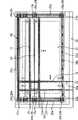
本实施方式的液晶显示装置,如图1、2所示,具有进行图像显示的俯视观察为矩形状的显示区域(图像显示区域)81,和不显示图像的四角形的框状的边缘区域82。在显示区域81中,由多个图像元素(子像素)构成的多个像素形成为矩阵状。边缘区域82是显示区域81外的区域,是包围显示区域81的全部外周的区域。The liquid crystal display device of this embodiment has, as shown in FIGS. 1 and 2 , a rectangular display region (image display region) 81 in plan view for displaying images, and a rectangular frame-shaped
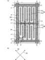
并且,图1中,虚线所围成的区域相当于显示区域81,由点划线围成的区域相当于一个图像元素。另外,在图1中,为了简化,只图示一个图像元素,实际上图像元素在上下左右排列为矩阵状。而且,图1中,涂有倾斜的斜线的区域表示接触孔。并且,图1、2中用涂有灰色的区域表示第三导电层。In addition, in FIG. 1 , the area enclosed by the dotted line corresponds to the
在各图像元素中形成有像素电极40和用于对像素电极40进行开关控制的薄膜晶体管(TFT)20。A
另外,在与源极驱动器(数据线驱动回路)连接的多个源极总线16电连接有各TFT20的源极17。源极驱动器经由源极总线16对各个图像元素供给图像信号。In addition, the
在与栅极驱动器(扫描线驱动回路)连接的多个栅极总线12电连接有各TFT20的栅极19。另外,从栅极驱动器在规定时刻向栅极总线12脉冲性地供给的扫描信号,以该顺序按照线序被施加于各TFT20。The
像素电极40电连接于TFT20的漏极18。从源极总线16供给的图像信号在规定时刻被施加于像素电极40,该像素电极40与通过扫描信号的输入只在一定期间为导通状态的TFT20相连接。由此,向液晶层60写入图像信号。The
向液晶层60写入的规定电平的图像信号,在被施加图像信号的像素电极40与在图像元素内与该像素电极40相对的共用电极(通用电极)50之间被保持一定期间。即,在这些电极40和50之间,一定期间里,形成电容(液晶电容)。在这里,为了防止所保持的图像信号泄漏,与液晶电容并列地形成有保持电容。保持电容在各图像元素中在TFT20的漏极18和Cs总线(电容保持配线)13之间形成。An image signal of a predetermined level written into the
接着,对本实施方式的液晶显示装置的更加详细的结构进行说明。本实施方式的液晶显示装置,具备液晶显示面板,和设置在液晶显示面板的背面侧的背光源单元(未图示)。液晶显示面板,如图3所示,具备有源矩阵基板(TFT阵列基板)10、与有源矩阵基板10相对的相对基板70、和夹持在它们之间的液晶层60。Next, a more detailed configuration of the liquid crystal display device of this embodiment will be described. The liquid crystal display device of this embodiment includes a liquid crystal display panel, and a backlight unit (not shown) provided on the rear side of the liquid crystal display panel. The liquid crystal display panel, as shown in FIG. 3 , includes an active matrix substrate (TFT array substrate) 10 , an opposing
有源矩阵基板10,在无色透明的绝缘基板11的一个(液晶层60一侧的)主面上具有:传达扫描信号的多个栅极总线12;多个Cs总线13;传达图像信号的多个源极总线16;作为开关元件,在各图像元素中各设置有一个的多个TFT20;在各TFT20各连接有一个的多个漏极18;在各图像元素个别地设置的多个像素电极40;在各图像元素共用地设置的共用电极50;和覆盖这些结构并设置在液晶层60一侧的表面的垂直取向膜30。The
另外,着眼于截面构造,有源矩阵基板10具有多个配线与多个绝缘层交替地层叠的构造。更加详细地说,有源矩阵基板10具有:在绝缘基板11的内主面侧(液晶层60一侧),形成有栅极总线12等的导电部件的第一层(第一导电层31)、栅极绝缘膜14、半导体层15、形成有源极总线16等的导电部件的第二层(第二导电层32)、在无机绝缘膜27的上层(液晶层60)一侧层叠有绝缘性树脂膜(有机绝缘膜)28的层间绝缘膜26、形成有共用电极50等的导电部件的第三层(第三导电层33)、和垂直取向膜30,从绝缘基板11一侧按照该顺序层叠的构造。In addition, focusing on the cross-sectional structure, the
第一导电层31和第二导电层32的各部件由铝等的金属膜形成。第三导电层33的各部件由ITO等的透明导电膜、铝、铬等的金属膜等形成。Each member of the first conductive layer 31 and the second conductive layer 32 is formed of a metal film such as aluminum. Each member of the third
绝缘基板11是有玻璃、石英、塑料等的透光性材料形成的基板(基体)。The insulating
各栅极总线12在左右方向上互相平行地延伸设置,各源极总线16在上下方向上互相平行地延伸设置。各Cs总线13在左右方向上互相平行地延伸设置。像这样,栅极总线12和Cs总线13互相交替地且平行地被配置。The
在本实施方式中,图像元素区域大致地规定为由这些栅极总线12和源极总线16包围的区域。另外,Cs总线13以通过各图像元素区域的中心附近的方式配置。In the present embodiment, the picture element region is roughly defined as a region surrounded by these
各栅极总线12的一个端伸出(延伸)到边缘区域82,在其前端分别连接有栅极端子21。在栅极端子21连接有栅极驱动的端子。另外,栅极总线12和栅极端子21形成在第一导电层31,并一体地(整体地)形成。One end of each
各源极总线16的一个端伸出(延伸)到显示区域81外、即伸出至边缘区域82,在其前端分别连接有源极端子22。在源极端子22连接有源极驱动器的端子。One end of each
源极总线16形成在第二导电层32,源极端子22形成在第一导电层31。源极总线16和源极端子22通过设置在栅极绝缘膜14的接触孔29a连接。The
各Cs总线13的两端(端部13a、13b)分别伸出(延伸)到边缘区域82的右侧和左侧的区域,并且宽度变宽。另外,端部13a彼此之间连接,并且端部13b彼此之间也连接。Both ends (end
更加详细地说,在与端部13a重叠的区域,在上下方向上设置有Cs连接配线(Cs主干)25a,在与端部13b重叠的区域,在上下方向上设置有Cs连接配线25b。Cs总线13形成在第一导电层31,Cs连接配线25a、25b形成在与第一导电层31不同的第二导电层32。More specifically, the Cs connection wiring (Cs main body) 25a is provided in the vertical direction in the area overlapping the
并且,Cs连接配线25a和端部13a通过设置在栅极绝缘膜14的接触孔29b连接,Cs连接配线25b和端部13b通过设置在栅极绝缘膜14的接触孔29c连接。The
另外,Cs连接配线25a和Cs连接配线25b互相连接。更加详细地说,在没有Cs连接配线25a、25b的边缘区域82的上侧的区域,在左右方向上设置有Cs连接配线25c,在没有Cs连接配线25a、25b的边缘区域82的下侧的区域,在左右方向上设置有Cs连接配线25d。Cs连接配线25c、25d形成在与Cs总线13和栅极总线12相同的第一导电层31。In addition, the
并且,Cs连接配线25c,通过设置在栅极绝缘膜14的接触孔29d与Cs连接配线25a的上侧的端连接,并且通过设置在栅极绝缘膜14的接触孔29e与Cs连接配线25b的上侧的端连接。另外,Cs配线25d通过设置在栅极绝缘膜14的接触孔29f与Cs连接配线25a的下侧的端连接,并且通过设置在栅极绝缘膜14的接触孔29g与Cs连接配线25b的下侧的端连接。Furthermore, the
由此,Cs总线13的两端(端部13a、13b)彼此连接,因此,能够从Cs总线13的两端(端部13a、13b)向显示区域内供给信号(共用信号)。Thus, both ends (ends 13a, 13b) of the
并且,在Cs连接配线25c的一个前端连有接Cs端子23a,在Cs连接配线25d的两端连接有Cs端子23b。在Cs端子23a、23b,连接有信号(共用信号)端子。Furthermore, a
其次,主要着眼于1个图像元素详细地对本实施方式的结构进行说明。Next, the configuration of the present embodiment will be described in detail mainly focusing on one image element.
像素电极40具有梳齿状的平面形状。更加具体地说,像素电极40具有像素主干部41和像素分支部42。The
像素主干部41是以平面地重叠于Cs总线13的方式配置的带状(俯视观察时为矩形状)的部分(主干部)。The
像素分支部42是连接干部21,并且设置在90°或270°方向的俯视观察时为线状的部分(分支部、梳齿)。The
像素主干部41和像素分支部42形成在第三导电层33,通过一体地(整体地)形成而连接。The pixel
共用电极50也在图像元素内具有俯视观察时为梳齿形状。更加具体地说,共用电极50具有共用边界部51、共用分支部52,和共用框部53。The
共用框部53是设置在显示区域81外的框状的部分。共用框部53通过设置在层间绝缘膜26的接触孔29h与Cs连接配线25a连接,并且通过设置在层间绝缘膜26的接触孔29i与Cs连接配线25b连接。而且,共用框部53通过贯通栅极绝缘膜14和层间绝缘膜26的接触孔29j与Cs连接配线25c连接,并且通过贯通栅极绝缘膜14和层间绝缘膜26的接触孔29k与Cs连接配线25d连接。The
即,共用框部53(共用电极50)通过Cs连接配线25a、25b、25c、25d连接于Cs总线13。由此,能够向Cs总线13和共用电极50供给(输入)相同的信号、即共用信号(公用信号)。因此,能够消减成本。That is, the common frame portion 53 (common electrode 50 ) is connected to the
另外,共用框部53(共用电极50)在显示区域81外与Cs总线13连接。即,用于连接Cs总线13和共用电极50的接触孔(接触孔29b、29d、29f、29h、29j、29k等)全部形成在显示区域81外。因此,因为也可以不用在显示区域81内(像素内)形成用于连接Cs总线13和共用电极50的接触孔,所以能够提高图像元素开口率,能够提高透过率。另外,由于没有必要在该图像元素内形成该接触孔,所以能够使Cs总线13的面积最小化,同样地,能够提高图像元素开口率,能够提高透过率。而且,由于该接触孔全部形成在显示区域81外,所以能够容易地增多其数量,增大其面积,因此,能够实现接触电阻的降低和防止信号延迟。In addition, the common frame portion 53 (common electrode 50 ) is connected to the
共用边界部(边界部)51是沿着相邻图像元素间的边界形成的部分。即,共用边界部51沿着栅极总线12和源极总线16形成。另外,共用边界部51以平面地与栅极总线12和源极总线16重叠的方式形成为格子状。The common boundary portion (boundary portion) 51 is a portion formed along the boundary between adjacent picture elements. That is,
另外,共用边界部51在显示区域81外与共用框部53连接。由此,从Cs端子23a、23b供给的共用信号通过Cs总线13、Cs连接配线25a、25b、25c、25d和共用框部53向显示区域81内供给。In addition, the
即,共用信号从上下左右4个方向输入到共用边界部51。另外,因为共用边界部51沿着栅极总线12和源极总线16形成,所以共用信号也沿着栅极总线12和源极总线16(栅极总线12和源极总线16的显示区域81的延伸方向)从上下左右4个方向输入。That is, the common signal is input to the
同样地,共用信号从俯视观察时为矩形状的显示区域的4边输入到显示区域内。Similarly, the common signal is input into the display area from four sides of the rectangular display area in plan view.
另外,共用边界部51以遮蔽由栅极总线12和源极总线16引起的电场的方式,在显示区域81内覆盖栅极总线12和源极总线16。由此,能够抑制由该电场引起的液晶分子发生取向不良,即抑制在图像元素内产生不良畴。In addition, the
并且,因为共用境界部51与栅极总线12和源极总线16重叠,所以能够提高图像元素开口率,提高透过率。In addition, since the
共用分支部(分支部,梳齿)52与共用边界部51连接,并且是从共用边界部51向图像元素中央延伸的俯视观察时为线状的部分。更加详细地说,共用分支部52从共用边界部51的与栅极总线12重叠的部分在90°或270°方向上形成。The common branch portion (branch portion, comb teeth) 52 is connected to the
共用框部53、共用边界部51和共用分支部52形成在第三导电层33,通过一体地(整体地)形成而连接。The
像这样,像素分支部42和共用分支部52具有互相互补的平面形状,并且具有某间隔互相不同地配置。即,像素分支部42和共用分支部52在同一平面内互相平行地对峙配置。而且换句话说,梳齿状的像素电极40和梳齿状的共用电极50以梳齿互相咬合的方式对置配置。另外,像素电极40和共用电极50配置在层间绝缘膜26(绝缘性树脂膜28)上的相同层(第三导电层33)。即,像素电极40和共用电极50配置在比栅极总线12和源极总线16更加靠液晶层60一侧。由此,在像素电极40和共用电极50之间能够高密度地形成横向电场,能够更加高精度地控制液晶层60,并且能够实现高透过率。另外,因为能够用相同的工序形成像素电极40和共用电极50,所以能够使制造工序简略化。In this way, the
并且,像素电极40和共用电极50在图像元素内,具有相对于通过图像元素中心的左右方向的中心线大致对称的平面形状。Furthermore, the
另外,像素分支部42的宽度(短边方向的长度)和共用分支部52的宽度(短边方向的长度),在相对的区域中全部是实质上相同的。In addition, the width (length in the short-side direction) of the
从增大透过率的观点看,优选像素分支部42和共用分支部52的宽度尽可能细,在现在的工艺规则中,优选设定为1~4μm(更加优选的是2.5~4.0μm)左右。From the viewpoint of increasing the transmittance, it is preferable that the width of the
电极间隔(像素分支部42和共用分支部52的间隙的宽度)S虽然没有特别地限定,但优选是2.5~20.0μm(更加优选的是4.0~12.0μm)。超过20.0μm,或不足2.5μm的话,透过率有可能降低。The electrode interval (the width of the gap between the
TFT20设置在栅极总线12和源极总线16的交叉部附近,具备栅极(栅极电极)19、半导体层15、源极(源极电极)17和漏极(漏极电极)18。
栅极19形成在第一导电层31,通过与栅极总线12一体(整体)地形成而与栅极总线12连接。The
栅极绝缘膜14以覆盖栅极总线12等的第一导电层31的方式,由氧化硅等的透明绝缘材料。The
半导体层15隔着栅极绝缘膜14在栅极19上形成为岛状,由非结晶硅膜形成。The semiconductor layer 15 is formed in an island shape on the
源极17的一个端部和漏极18的一个端部分别平面地重叠(搭置)在半导体层15上。另外,源极17形成在第二导电层32上,通过与源极总线16一体(整体)地形成而与源极总线16连接。即,源极17是从源极总线16分支并向半导体层15延伸的配线,连接源极总线16和TFT20。One end portion of the
漏极18从半导体层15延伸,具有俯视观察时大致为L字状的配线。另外,漏极18与源极17同样地形成在第二导电层32。The
像这样,TFT20是用在分离漏极18和源极17时,对导体层15稍微进行蚀刻的制法制造的沟道蚀刻型,并且,是栅极19被设置在漏极18和源极17的更下方(绝缘基板11侧)的反交错(stagger)型。As such, the
另外,栅极总线12和Cs总线13,可以形成在相比于源极总线16更靠液晶层60一侧。例如,可以从绝缘基板11侧按顺序依次层叠半导体层15、栅极绝缘膜14、栅极总线12以及Cs总线13、由无机绝缘膜等的透明绝缘材料构成的层间绝缘膜、源极总线16、层间绝缘膜26、像素电极40和共用电极50。该情况下,作为TFT20,可以形成栅极19设置在相比于漏极18和源极17更靠液晶层60一侧的正交错型、共面型的TFT。In addition, the
另外,漏极18与像素电极40连接,并且形成保持电容。更加详细地说,漏极18在与TFT20相反侧的端部(L字的前端部)具有带状(俯视观察时为矩形状)的保持电容部24。保持电容部24与Cs总线13平面地重叠形成。而且,在保持电容部24和Cs总线13平面地重叠的区域,形成有以这些保持电容部24和Cs总线13为电极的保持电容。另外,保持电容部24与像素主干部41平面地重叠配置,并且通过设置在层间绝缘膜26的接触孔29m与像素主干部41连接。即,像素电极40通过设置在层间绝缘膜26的接触孔29m与漏极18连接。In addition, the
层间绝缘膜26以覆盖半导体层15和源极17、源极总线16、漏极18等的第二导电层32的各部件的方式设置。The
另外,无机绝缘膜27利用CVD法由氧化硅等的透明绝缘材料形成,绝缘性树脂膜28由感光性的丙烯酸树脂等的透明绝缘材料形成。In addition, the inorganic insulating
在这里,对层间绝缘膜26的形成方法进行说明,首先,形成膜厚1500~4000
另外,一般的丙烯酸树脂的相对介电常数是2.7~4.5(优选的是3.4~3.8),比无机绝缘膜的相对介电常数(例如,氮化硅的相对介电常数8)低。另外,能够提高其透明度,并且通过旋涂法能够容易地形成数μm左右厚度的膜厚。总之,按照本实施方式,能够有效地减小上层的第三导电层33的各部件与下层的第一导电层31和第二导电层32的各部件之间的电容成分。其结果,能够抑制图像信号等的信号的延迟。另外,能够抑制电容成分的增加,并且能够如上所述将共用边界部51与栅极总线12和源极总线16重叠,能够提高图像元素开口率。In addition, the relative permittivity of general acrylic resins is 2.7 to 4.5 (preferably 3.4 to 3.8), which is lower than that of inorganic insulating films (for example, the relative permittivity of silicon nitride is 8). In addition, the transparency can be improved, and a film thickness of about several μm can be easily formed by the spin coating method. In short, according to this embodiment, it is possible to effectively reduce the capacitance component between each member of the upper third
另外,由于使用感光性的树脂膜,在树脂模的图案化中不需要光致抗蚀剂工序,因此,在生产性的方面是有利的。In addition, since a photosensitive resin film is used, a photoresist step is not required for patterning a resin mold, which is advantageous in terms of productivity.
另外,绝缘树脂膜28的膜厚虽然没有特别地限定,但是优选设定为2~5μm(更加优选的是3.5~4.5μm)左右。不足2μm时,电容成分有可能变大。超过5μm时,透过率的降低有可能变大。In addition, the film thickness of the insulating resin film 28 is not particularly limited, but is preferably set to about 2 to 5 μm (more preferably 3.5 to 4.5 μm). When the thickness is less than 2 μm, the capacitance component may become large. When it exceeds 5 μm, there is a possibility that the decrease in transmittance becomes large.
并且,覆盖像素电极40和共用电极50形成聚酰亚胺等的垂直取向膜30。Further, a
相对基板70,在无色透明的绝缘基板71的一个(液晶层60侧的)主面上,具有:对相邻图像元素之间和边缘区域82遮光的黑矩阵(BM)层(未图示);对应各图像元素设置的多个色层(彩色滤光片,未图示);和覆盖这些结构并设置在液晶层60一侧的表面的垂直取向膜72。Opposed to the
绝缘基板71是由玻璃、石英、塑料等的透过性材料形成的基板(基体)。The insulating
BM层由Cr等的不透明的金属、含有碳的丙烯酸树脂等的不透明的有机膜等形成。另外,BM层在显示区域81内形成在图像元素区域的周围,即对应栅极总线12和源极总线16的区域。The BM layer is formed of an opaque metal such as Cr, an opaque organic film such as an acrylic resin containing carbon, or the like. In addition, the BM layer is formed around the picture element area in the
色层是用于进行彩色显示的层,由含有颜料的丙烯酸树脂等的透明的有机膜等形成,主要形成在图像元素区域。The colored layer is a layer for color display, and is formed of a transparent organic film such as acrylic resin containing a pigment, and is mainly formed in a picture element region.
垂直取向膜30、72分别由聚酰亚胺等的周知的取向膜材料涂敷形成。垂直取向膜30、72通常不进行研磨处理,在未施加电压时,能够使液晶分子相对于膜表面大致垂直地取向。The
像这样,本实施方式的液晶显示装置是在相对基板70上具备色层的彩色液晶显示装置(彩色显示的有源矩阵型液晶显示装置),由输出R(红)、G(绿)、B(蓝)的各色的光的3个图像元素构成1个像素。As such, the liquid crystal display device of this embodiment is a color liquid crystal display device (active matrix type liquid crystal display device for color display) provided with a colored layer on the
并且,不特别限定构成各像素的图像元素的颜色的种类和数量,能够适当地设定。即,在本实施方式的液晶显示装置中,各像素,例如、可以由青色、品红色和黄色这3色的图像元素构成,也可以由4色以上的图像元素构成。另外,本实施方式的液晶显示装置也可以是黑白显示。Furthermore, the type and number of colors of picture elements constituting each pixel are not particularly limited, and can be appropriately set. That is, in the liquid crystal display device of the present embodiment, each pixel may be composed of, for example, three color picture elements of cyan, magenta, and yellow, or may be composed of four or more color picture elements. In addition, the liquid crystal display device of this embodiment may also display in black and white.
另外,在BM层和色层的液晶层60一侧,为了使这些结构的台阶差平坦化,优选进一步层叠由透明树脂材料等形成的平坦化膜(底膜)。由此,能够使相对基板70表面平坦化并且使液晶层60的厚度均一化,能够防止在图像元素区域内驱动电压变得不均匀,能够防止对比度降低。In addition, on the
有源矩阵基板10和相对基板70隔着塑料珠等的隔离物,通过以包围显示区域81的方式设置的密封剂而贴合。并且,在有源矩阵基板10和相对基板70之间的空隙,通过封入作为构成光学调制层的显示用介质的液晶材料而形成液晶层60。The
液晶层60含有具有正的介电常数各向异性的向列型液晶材料(p型向列型液晶材料)。p型向列型液晶材料的液晶分子,通过有源矩阵基板10和相对基板70的垂直取向膜30、72的取向控制力,在未施加电压时(没有产生由像素电极40和共用电极50所产生的电场时),显示垂直取向。更加具体地说,垂直取向膜30、72附近的p型向列型液晶材料的液晶分子的长轴,在未施加电压时,相对于有源矩阵基板10和相对基板70面分别具有88°以上(更优选的是89°以上)的角。The
另外,在有源矩阵基板10的外主面侧(与液晶层60相反侧),粘贴有偏光板35,在相对基板70的外主面侧粘贴有偏光板73。并且,本实施方式的液晶显示装置可以具有相位差板、视角补偿薄膜。In addition, the
本实施方式的液晶显示装置的各光学轴的配置,如图2(b)所示。有源矩阵基板10一侧的偏光板31的透过轴31t和相对基板70一侧的偏光板73的透过轴73t,在俯视观察时都以相对于像素分支部42和共用分支部52成45°的角的方式配置。透过轴35t和透过轴73t,在俯视观察时,朝向倾斜45°方向配置为正交尼克尔。The arrangement of the optical axes of the liquid crystal display device of this embodiment is as shown in FIG. 2( b ). The transmission axis 31t of the polarizing plate 31 on the side of the
具备上述结构的本实施方式的液晶显示装置,通过经由TFT20向像素电极40施加图像信号(电压),在像素电极40和共用电极50之间,产生与基板10、70面方向、即与基板10、70面平行的电场(横向电场)。并且,通过该横向电场驱动液晶,使各图像元素的透过率变化进行图像显示。In the liquid crystal display device of the present embodiment having the above-mentioned structure, by applying an image signal (voltage) to the
更加详细地说,本实施方式的液晶显示装置,通过电场的施加,在液晶层60内形成电场强度的分布,并利用由此所产生的液晶分子的排列的偏斜使液晶层60的相位延迟变化。进一步详细地说,液晶层60的初始取向状态是垂直取向,通过对梳齿状的像素电极40和共用电极50施加电压,使得在液晶层60内产生横向电场,形成弯曲状的电场。其结果是,如图4所示,形成互相的主导方向相差180°的2个畴,并且在各畴内(各电极间),向列型液晶材料的液晶分子显示弯曲状的液晶排列(弯曲取向)。More specifically, in the liquid crystal display device of this embodiment, the distribution of the electric field intensity is formed in the
以上,按照本实施方式,共用电极50在显示区域81中配置在与形成有栅极总线12和源极总线16的层(第一导电层31和第二导电层32)不同的层(第三导电层33)。因此,如上所述,能够不影响栅极总线12和源极总线16的布局而更加自由地设计共用电极50的布局。因此,能够从比现有技术更多的方向(至少3方向),具体地说从图1中的镂空箭头所示的方向,向显示区域81输入共用信号。即,在现有技术中最多只能从显示区域的2边向显示区域内输入共用信号,在本实施方式中,能够从显示区域的3边以上(更优选的是4边)向显示区域内输入共用信号。另外,从比现有技术更多的方向(至少3方向),具体地说从图2(a)中的镂空的箭头所示的方向向图像元素中也输入共用信号。其结果,能够抑制因附加电容导致在共用信号中产生噪音。因此,能够抑制图像闪烁,抑制产生相对暗的部分(阴影)。像素越是高精细该效果越大。As described above, according to the present embodiment, the
另外,共用电极50,在显示区域81外、即在边缘区域82中,具有在俯视观察时与栅极总线12和源极总线16交叉的部分。由此,如上所述,能够以围绕显示区域81的外周的方式形成共用框部53,能够至少从3个方向向显示区域81内有效地输入共用信号。In addition, the
而且,在本实施方式中,共用框部53包围显示区域81的全部外周。由此,能够从4个方向(本实施方式的上下左右方向)向显示区域81内有效地输入共用信号。Furthermore, in the present embodiment, the
另一方面,共用框部53可以以只包围显示区域81的三边的方式形成为コ字(U字)状。由此,也能够从比在现有技术中更多的3个方向(例如,上下和右方向、上下和左方向、左右和上方向,或左右和下方向)向显示区域81内输入共用信号。另外,与此同时,如果省略Cs连接配线25c或Cs连接配线25b,则能够减小边缘区域82。On the other hand, the
另外,虽然以TBA为例对本实施方式的液晶显示装置进行了详细地说明,但是本实施方式的液晶显示装置也可以是IPS模式的液晶显示装置。这时,代替垂直取向膜30、72形成水平取向膜,并且在该水平取向膜进行研磨处理,而且,作为p型向列型液晶材料,在未施加电压时,可以使用相对于有源矩阵基板10和相对基板70面大致平行地取向的材料。由此,也能够起到与在TBA模式的情况下相同的效果。In addition, although the liquid crystal display device of this embodiment has been described in detail by taking TBA as an example, the liquid crystal display device of this embodiment may be an IPS mode liquid crystal display device. At this time, a horizontal alignment film is formed instead of the
并且,本实施方式的液晶显示装置,可以是反射型,也可以是半透过型(反射透过两用型)。Furthermore, the liquid crystal display device of the present embodiment may be a reflective type or a transflective type (reflective and transmissive type).
(实施方式2)(Embodiment 2)
本实施方式的液晶显示装置,在以下方面与实施方式1不同。The liquid crystal display device of this embodiment differs from Embodiment 1 in the following points.
即,本实施方式的液晶显示装置在相对基板侧具有相对电极。具体来说,如图5所示,在绝缘基板71的液晶层60一侧的主面上,相对电极61、电介质层(绝缘层)62和垂直取向膜72按照该顺序层叠。并且,在相对电极61和绝缘基板71之间可以设置多个色层(彩色滤光片)和/或黑矩阵(BM)层。That is, the liquid crystal display device of the present embodiment has a counter electrode on the counter substrate side. Specifically, as shown in FIG. 5 , on the main surface of the insulating
相对电极61,由ITO、IZO等的透明导电膜形成。相对电极61和电介质层62,分别以至少覆盖显示区域81的全部的方式无缝隙地形成。向相对电极61施加在各图像元素(子像素)中共通的规定的电位。The
电介质层62由透明的绝缘材料形成。具体地说,由氮化硅等的无机绝缘膜、丙烯酸树脂等的有机绝缘膜等形成。The
另一方面,在绝缘基板11中,与实施方式1形同,设置有包括像素电极40和共用电极50的梳齿状的电极和垂直取向膜30。另外,在2个绝缘基板11、71的外主面上配置有偏光板35、73。On the other hand, in the same manner as in the first embodiment, the insulating
在黑显示时以外,在像素电极40与共用电极50和相对电极61之间施加不同的电压。共用电极50和相对电极61可以被接地,在共用电极50和相对电极61也可以施加相同大小和极性的电压,也可以施加不同大小和极性的电压。Different voltages are applied between the
在本实施方式的液晶显示装置中,与实施方式1相同,能够抑制因附加电容导致的显示品质的低下。另外,通过形成相对电极61,能够提高响应速度。In the liquid crystal display device of the present embodiment, as in the first embodiment, it is possible to suppress a decrease in display quality due to the additional capacitance. In addition, the response speed can be improved by forming the
本申请,以在2009年5月13日申请的日本国专利申请2009-116786号,和在2010年1月15日申请的日本国专利申请2010-6696号为基础,主张基于巴黎条约和进入国的法规的优先权。这些申请的内容的全部作为参考组合在本申请中。This application is based on Japanese Patent Application No. 2009-116786 filed on May 13, 2009, and Japanese Patent Application No. 2010-6696 filed on January 15, 2010, claiming that it is based on the Paris Treaty and the country of entry. the priority of the regulations. All the contents of these applications are incorporated in this application as a reference.
符号说明Symbol Description
10:有源矩阵基板10: Active matrix substrate
11、71:绝缘基板11, 71: insulating substrate
12:栅极总线12: Gate bus
13:Cs总线13: Cs bus
13a、13b:Cs总线的端部13a, 13b: ends of the Cs bus
14:栅极绝缘膜14: Gate insulating film
15:半导体层15: Semiconductor layer
16:源极总线16: Source bus
17:源极17: Source
18:漏极18: drain
19:栅极19: grid
20:TFT20: TFT
21:栅极端子21: Gate terminal
22:源极端子22: Source terminal
23a、23b:Cs端子23a, 23b: Cs terminal
24:保持电容部24: holding capacitor part
25a、25b、25c、25d:Cs连接配线25a, 25b, 25c, 25d: Cs connection wiring
26:层间绝缘膜26: Interlayer insulating film
27:无机绝缘膜27: Inorganic insulating film
28:绝缘性树脂模28: Insulating resin mold
29a、29b、29c、29d、29e、29f、29g、29h、29i、29j、29k、29m:接触孔29a, 29b, 29c, 29d, 29e, 29f, 29g, 29h, 29i, 29j, 29k, 29m: contact holes
30、72:垂直取向膜30, 72: vertical alignment film
31:第一导电层31: The first conductive layer
32:第二导电层32: Second conductive layer
33:第三导电层33: The third conductive layer
34:共用信号34: Common signal
40:像素电极40: Pixel electrode
41:像素主干部41: Pixel backbone
42:像素分支部42: Pixel branch
50:共用电极50: common electrode
51:共用边界部51: shared border
52:共用分支部52: Shared branch
53:共用框部53: Common frame part
60:液晶层60: liquid crystal layer
61:相对电极61: opposite electrode
62:电介质层62: Dielectric layer
70:相对基板70: relative substrate
35、73:偏光板35, 73: polarizer
35t、73t:偏光板的透过轴35t, 73t: transmission axis of polarizer
81:显示区域81: display area
82:边缘区域82: Edge area
Claims (24)
Translated fromChineseApplications Claiming Priority (5)
| Application Number | Priority Date | Filing Date | Title |
|---|---|---|---|
| JP2009-116786 | 2009-05-13 | ||
| JP2009116786 | 2009-05-13 | ||
| JP2010006696 | 2010-01-15 | ||
| JP2010-006696 | 2010-03-18 | ||
| PCT/JP2010/057016WO2010131552A1 (en) | 2009-05-13 | 2010-04-20 | Liquid crystal display device |
Publications (1)
| Publication Number | Publication Date |
|---|---|
| CN102422210Atrue CN102422210A (en) | 2012-04-18 |
Family
ID=43084929
Family Applications (1)
| Application Number | Title | Priority Date | Filing Date |
|---|---|---|---|
| CN2010800205209APendingCN102422210A (en) | 2009-05-13 | 2010-04-20 | Liquid crystal display device |
Country Status (3)
| Country | Link |
|---|---|
| US (1) | US20120062451A1 (en) |
| CN (1) | CN102422210A (en) |
| WO (1) | WO2010131552A1 (en) |
Cited By (2)
| Publication number | Priority date | Publication date | Assignee | Title |
|---|---|---|---|---|
| CN108445684A (en)* | 2018-02-27 | 2018-08-24 | 上海中航光电子有限公司 | Array substrate, display panel and display device |
| CN114167651A (en)* | 2021-12-10 | 2022-03-11 | Tcl华星光电技术有限公司 | Liquid crystal display panel |
Families Citing this family (6)
| Publication number | Priority date | Publication date | Assignee | Title |
|---|---|---|---|---|
| JP5530987B2 (en)* | 2011-08-09 | 2014-06-25 | 株式会社ジャパンディスプレイ | Liquid crystal display |
| CN102854670B (en)* | 2012-06-01 | 2015-10-21 | 京东方科技集团股份有限公司 | Liquid crystal display method of controlling viewing angle, display panels and liquid crystal display |
| DE102013206039A1 (en) | 2013-04-05 | 2014-10-09 | Wobben Properties Gmbh | Wind energy plant and method for operating a wind energy plant |
| KR20150122897A (en)* | 2014-04-23 | 2015-11-03 | 삼성디스플레이 주식회사 | Display device and manufacturing method thereof |
| CN105977263A (en)* | 2016-05-31 | 2016-09-28 | 京东方科技集团股份有限公司 | Array substrate, production method thereof, display panel, and display device |
| CN110850654B (en)* | 2019-11-27 | 2020-12-04 | 深圳市华星光电半导体显示技术有限公司 | Liquid crystal display panel |
Citations (5)
| Publication number | Priority date | Publication date | Assignee | Title |
|---|---|---|---|---|
| JPH10186351A (en)* | 1996-12-24 | 1998-07-14 | Hitachi Ltd | Liquid crystal display |
| US6128061A (en)* | 1997-12-08 | 2000-10-03 | Hyundai Electronics Industries Co., Ltd. | Liquid crystal display device |
| JP2002323706A (en)* | 2001-02-23 | 2002-11-08 | Nec Corp | Active matrix liquid crystal display device of transverse electric field system and method for manufacturing the same |
| JP2004226549A (en)* | 2003-01-21 | 2004-08-12 | Hitachi Displays Ltd | Liquid crystal display |
| US20050105033A1 (en)* | 2003-09-29 | 2005-05-19 | Hitachi Displays, Ltd. | Liquid crystal display panel |
Family Cites Families (8)
| Publication number | Priority date | Publication date | Assignee | Title |
|---|---|---|---|---|
| WO1998047044A1 (en)* | 1997-04-11 | 1998-10-22 | Hitachi, Ltd. | Liquid crystal display device |
| JP2003307748A (en)* | 2002-04-15 | 2003-10-31 | Advanced Display Inc | Liquid crystal display device and manufacturing method thereof |
| JP4293867B2 (en)* | 2003-09-05 | 2009-07-08 | 奇美電子股▲ふん▼有限公司 | IPS liquid crystal display corresponding to pixel enlargement |
| KR100958246B1 (en)* | 2003-11-26 | 2010-05-17 | 엘지디스플레이 주식회사 | Transverse electric field type liquid crystal display device and manufacturing method thereof |
| JP4462981B2 (en)* | 2004-03-29 | 2010-05-12 | Nec液晶テクノロジー株式会社 | Active matrix substrate and liquid crystal display device including the substrate |
| JP2007279634A (en)* | 2006-04-12 | 2007-10-25 | Nec Lcd Technologies Ltd | Horizontal electric field type liquid crystal display device |
| JP4449953B2 (en)* | 2006-07-27 | 2010-04-14 | エプソンイメージングデバイス株式会社 | Liquid crystal display |
| JP2009122474A (en)* | 2007-11-16 | 2009-06-04 | Mitsubishi Electric Corp | Liquid crystal display device and manufacturing method thereof |
- 2010
- 2010-04-20USUS13/319,399patent/US20120062451A1/ennot_activeAbandoned
- 2010-04-20WOPCT/JP2010/057016patent/WO2010131552A1/enactiveApplication Filing
- 2010-04-20CNCN2010800205209Apatent/CN102422210A/enactivePending
Patent Citations (5)
| Publication number | Priority date | Publication date | Assignee | Title |
|---|---|---|---|---|
| JPH10186351A (en)* | 1996-12-24 | 1998-07-14 | Hitachi Ltd | Liquid crystal display |
| US6128061A (en)* | 1997-12-08 | 2000-10-03 | Hyundai Electronics Industries Co., Ltd. | Liquid crystal display device |
| JP2002323706A (en)* | 2001-02-23 | 2002-11-08 | Nec Corp | Active matrix liquid crystal display device of transverse electric field system and method for manufacturing the same |
| JP2004226549A (en)* | 2003-01-21 | 2004-08-12 | Hitachi Displays Ltd | Liquid crystal display |
| US20050105033A1 (en)* | 2003-09-29 | 2005-05-19 | Hitachi Displays, Ltd. | Liquid crystal display panel |
Cited By (4)
| Publication number | Priority date | Publication date | Assignee | Title |
|---|---|---|---|---|
| CN108445684A (en)* | 2018-02-27 | 2018-08-24 | 上海中航光电子有限公司 | Array substrate, display panel and display device |
| CN114167651A (en)* | 2021-12-10 | 2022-03-11 | Tcl华星光电技术有限公司 | Liquid crystal display panel |
| CN114167651B (en)* | 2021-12-10 | 2023-10-31 | Tcl华星光电技术有限公司 | Liquid crystal display panel having a light shielding layer |
| US12158667B2 (en) | 2021-12-10 | 2024-12-03 | Tcl China Star Optoelectronics Technology Co., Ltd. | Liquid crystal display panel |
Also Published As
| Publication number | Publication date |
|---|---|
| WO2010131552A1 (en) | 2010-11-18 |
| US20120062451A1 (en) | 2012-03-15 |
Similar Documents
| Publication | Publication Date | Title |
|---|---|---|
| US11774809B2 (en) | Liquid crystal display panel | |
| US7973900B2 (en) | Liquid crystal display device | |
| US8614779B2 (en) | Lateral electric field type active-matrix addressing liquid crystal display device | |
| JP4667587B2 (en) | Liquid crystal display device | |
| JP5344253B2 (en) | Horizontal electric field type liquid crystal display device | |
| JP4162890B2 (en) | Liquid crystal display | |
| US8736781B2 (en) | Liquid crystal display device and method of driving the same | |
| WO2009119798A1 (en) | Liquid crystal display device | |
| CN102422210A (en) | Liquid crystal display device | |
| JP5429776B2 (en) | LCD panel | |
| US10768495B2 (en) | Display device having a first electrode with an opening overlapping with a second electrode | |
| KR102098161B1 (en) | Array substrate for liquid crystal display | |
| JP2019128429A (en) | Liquid crystal display unit | |
| JP5258603B2 (en) | Liquid crystal display | |
| US7855771B2 (en) | Liquid crystal display panel and active matrix substrate thereof | |
| JP5534655B2 (en) | ELECTRO-OPTICAL DEVICE, MANUFACTURING METHOD THEREOF, AND ELECTRONIC DEVICE | |
| TWI754388B (en) | Liquid crystal display device | |
| JP4441507B2 (en) | Liquid crystal display | |
| JP3282542B2 (en) | Active matrix type liquid crystal display | |
| US9030635B2 (en) | Liquid crystal display device comprising a stage having an electrode formation surface | |
| WO2021206084A1 (en) | Liquid crystal display device | |
| JP2014235420A (en) | Liquid crystal display panel, electronic apparatus, and method for manufacturing pixel substrate | |
| JP2007264232A (en) | Liquid crystal display and electronic device | |
| JP2008083209A (en) | Liquid crystal device, manufacturing method thereof, and electronic apparatus | |
| KR20040034745A (en) | In-Plane Switching mode Liquid Crystal Display Device |
Legal Events
| Date | Code | Title | Description |
|---|---|---|---|
| C06 | Publication | ||
| PB01 | Publication | ||
| C10 | Entry into substantive examination | ||
| SE01 | Entry into force of request for substantive examination | ||
| C02 | Deemed withdrawal of patent application after publication (patent law 2001) | ||
| WD01 | Invention patent application deemed withdrawn after publication | Application publication date:20120418 |