CN102422172A - Non-contact testing of printed electronic devices - Google Patents
Non-contact testing of printed electronic devicesDownload PDFInfo
- Publication number
- CN102422172A CN102422172ACN2010800208917ACN201080020891ACN102422172ACN 102422172 ACN102422172 ACN 102422172ACN 2010800208917 ACN2010800208917 ACN 2010800208917ACN 201080020891 ACN201080020891 ACN 201080020891ACN 102422172 ACN102422172 ACN 102422172A
- Authority
- CN
- China
- Prior art keywords
- test circuit
- substrate
- energy
- light
- printing
- Prior art date
- Legal status (The legal status is an assumption and is not a legal conclusion. Google has not performed a legal analysis and makes no representation as to the accuracy of the status listed.)
- Granted
Links
Images


Classifications
- G—PHYSICS
- G01—MEASURING; TESTING
- G01R—MEASURING ELECTRIC VARIABLES; MEASURING MAGNETIC VARIABLES
- G01R31/00—Arrangements for testing electric properties; Arrangements for locating electric faults; Arrangements for electrical testing characterised by what is being tested not provided for elsewhere
- G01R31/28—Testing of electronic circuits, e.g. by signal tracer
- G01R31/302—Contactless testing
- G01R31/308—Contactless testing using non-ionising electromagnetic radiation, e.g. optical radiation
- G01R31/309—Contactless testing using non-ionising electromagnetic radiation, e.g. optical radiation of printed or hybrid circuits or circuit substrates
- G—PHYSICS
- G01—MEASURING; TESTING
- G01R—MEASURING ELECTRIC VARIABLES; MEASURING MAGNETIC VARIABLES
- G01R31/00—Arrangements for testing electric properties; Arrangements for locating electric faults; Arrangements for electrical testing characterised by what is being tested not provided for elsewhere
- G01R31/28—Testing of electronic circuits, e.g. by signal tracer
- G01R31/2801—Testing of printed circuits, backplanes, motherboards, hybrid circuits or carriers for multichip packages [MCP]
- G01R31/2806—Apparatus therefor, e.g. test stations, drivers, analysers, conveyors
- G01R31/2808—Holding, conveying or contacting devices, e.g. test adapters, edge connectors, extender boards
- G—PHYSICS
- G01—MEASURING; TESTING
- G01R—MEASURING ELECTRIC VARIABLES; MEASURING MAGNETIC VARIABLES
- G01R31/00—Arrangements for testing electric properties; Arrangements for locating electric faults; Arrangements for electrical testing characterised by what is being tested not provided for elsewhere
- G01R31/28—Testing of electronic circuits, e.g. by signal tracer
- G01R31/302—Contactless testing
- G01R31/304—Contactless testing of printed or hybrid circuits
- G—PHYSICS
- G01—MEASURING; TESTING
- G01R—MEASURING ELECTRIC VARIABLES; MEASURING MAGNETIC VARIABLES
- G01R31/00—Arrangements for testing electric properties; Arrangements for locating electric faults; Arrangements for electrical testing characterised by what is being tested not provided for elsewhere
- G01R31/28—Testing of electronic circuits, e.g. by signal tracer
- G01R31/2801—Testing of printed circuits, backplanes, motherboards, hybrid circuits or carriers for multichip packages [MCP]
- G01R31/281—Specific types of tests or tests for a specific type of fault, e.g. thermal mapping, shorts testing
- G01R31/2812—Checking for open circuits or shorts, e.g. solder bridges; Testing conductivity, resistivity or impedance
Landscapes
- Engineering & Computer Science (AREA)
- Physics & Mathematics (AREA)
- General Engineering & Computer Science (AREA)
- General Physics & Mathematics (AREA)
- Health & Medical Sciences (AREA)
- Computer Vision & Pattern Recognition (AREA)
- Electromagnetism (AREA)
- Toxicology (AREA)
- Computer Hardware Design (AREA)
- Microelectronics & Electronic Packaging (AREA)
- Investigating Materials By The Use Of Optical Means Adapted For Particular Applications (AREA)
- Testing Of Short-Circuits, Discontinuities, Leakage, Or Incorrect Line Connections (AREA)
- Testing Electric Properties And Detecting Electric Faults (AREA)
- Testing Of Optical Devices Or Fibers (AREA)
- Tests Of Electronic Circuits (AREA)
- Accessory Devices And Overall Control Thereof (AREA)
- Electroluminescent Light Sources (AREA)
Abstract
Translated fromChineseDescription
Translated fromChinese对先前提交的美国申请的权益要求Claims to Benefits of Previously Filed U.S. Applications
本申请要求2009年5月8日提交的美国申请S/N 12/437,779的权益。该文件以及本文提及的出版物、专利和专利文件的整个公开的内容通过引用结合于此。This application claims the benefit of U.S. Application S/N 12/437,779, filed May 8, 2009. The entire disclosures of this document, as well as the publications, patents, and patent documents mentioned herein are hereby incorporated by reference.
技术领域technical field
本公开涉及在例如薄玻璃基板之类的基板上印刷电子器件,且尤其涉及这些基板上的印刷电子器件的非接触测试。The present disclosure relates to printing electronic devices on substrates, such as thin glass substrates, and in particular to non-contact testing of printed electronic devices on these substrates.
背景技术Background technique
电子纸——也称为ePaper——是预期未来几年将广泛使用的新的显示种类。显示器工作在反射模式中且是双稳态的,即,它具有两个稳定状态。如此,显示器使用低功率,一般仅需要用于改变图像的功率且几乎不需要用于维持图像的功率。Electronic paper - also known as ePaper - is a new type of display that is expected to become widely used in the next few years. The display works in reflective mode and is bistable, ie it has two stable states. As such, the display uses low power, typically requiring only power to change the image and little power to maintain the image.
由于它们与普通的印刷纸(最常见的显示形式)竞争,必须使ePaper(电子纸)显示器低成本。因此,类似于普通的印刷纸,需要通过印刷工艺制造ePaper。具体地,生产在ePaper显示器中使用的电子器件的制造工艺需要是印刷工艺,或者在单个板上或者在卷上,例如卷装进出工艺。可预期印刷速度类似于报纸和杂志生产中使用的速度,例外是与普通墨不同,电子墨将用于生产ePaper显示器中使用的电子电路。Since they compete with ordinary printed paper (the most common form of display), ePaper (electronic paper) displays must be made low cost. Therefore, similar to ordinary printing paper, ePaper needs to be manufactured through a printing process. Specifically, the manufacturing process to produce the electronics used in ePaper displays needs to be a printing process, either on a single board or on a roll, such as a roll-to-roll process. Printing speeds are expected to be similar to those used in newspaper and magazine production, with the exception that, unlike regular ink, electronic ink will be used to produce the electronic circuits used in ePaper displays.
通过印刷以高速生产显示器的主要结果是在非常短的时间内形成大量显示器。因此,需要一种获悉显示器是否良好且工艺是否在控制之中的方式。否则,将会非常快地产生大量废料。因此关键是在制造显示器时知晓印刷机上的印刷电子器件的质量。本公开解决该关键需要,以便在广泛的工业规模上成功采用ePaper显示器。A major consequence of producing displays at high speeds by printing is the formation of large numbers of displays in a very short time. Therefore, there is a need for a way to know if the display is good and the process is under control. Otherwise, a lot of waste will be generated very quickly. It is therefore critical to know the quality of the printed electronics on the printing press when the display is being manufactured. The present disclosure addresses this critical need for successful adoption of ePaper displays on a broad industrial scale.
发明内容Contents of the invention
根据第一方面,公开了一种用于测试基板(3)上电子组件的印刷的非接触方法,包括:According to a first aspect, a non-contact method for testing the printing of electronic components on a substrate (3) is disclosed, comprising:
(A)在基板(3)上印刷(i)电子组件和(ii)测试电路(11),其中测试电路(11)包括:(A) printing (i) electronic components and (ii) test circuit (11) on the substrate (3), wherein the test circuit (11) includes:
(a)用于为测试电路(11)提供电能的第一部分(13);(a) a first part (13) for powering the test circuit (11);
(b)用于产生可检测的光信号的第二部分(15),所述信号指示电子组件的至少一个电学性质;以及(b) a second portion (15) for generating a detectable optical signal indicative of at least one electrical property of the electronic component; and
(c)连接第一(13)和第二(15)部分的电路;以及(c) a circuit connecting the first (13) and second (15) parts; and
(B)在第一部分(13)提供电能;以及(B) provide electrical energy in the first part (13); and
(C)检测第二部分(15)的可检测光学信号。(C) detecting a detectable optical signal of the second portion (15).
根据第二方面,公开用于印刷电子组件的装置,包括:According to a second aspect, an apparatus for printing electronic components is disclosed, comprising:
(a)用于在基板(3)上印刷(i)电子组件和(ii)测试电路(11)的装置;以及(a) apparatus for printing (i) electronic components and (ii) test circuits (11) on a substrate (3); and
(b)用于检测来自基板(3)的区域(15)的光的光检测器(25),所述光指示所述电子组件的至少一个电学性质。(b) A light detector (25) for detecting light from a region (15) of the substrate (3), said light being indicative of at least one electrical property of said electronic component.
根据第三方面,公开一种基板(3),包括(i)印刷电子组件和(ii)印刷测试电路(11),其中测试电路(11)包括:According to a third aspect, a substrate (3) is disclosed comprising (i) printed electronic components and (ii) printed test circuitry (11), wherein the test circuitry (11) comprises:
(a)用于为测试电路(11)提供电能的第一部分(13);(a) a first part (13) for powering the test circuit (11);
(b)用于产生可检测的光信号的第二部分(15),所述信号指示电子组件的至少一个电学性质;以及(b) a second portion (15) for generating a detectable optical signal indicative of at least one electrical property of the electronic component; and
(c)连接第一(13)和第二(15)部分的电路。(c) A circuit connecting the first (13) and second (15) parts.
在以上本公开的各方面的概要中使用的附图标记仅仅用于方便读者,而不打算且不应该解释为限制本发明的范围。更一般而言,可以理解,以上的一般描述和以下的详细描述两者仅仅是对本发明的示例性说明,并且它们旨在提供用于理解本发明的本质和特性的概观或框架。The reference numerals used in the above summary of aspects of the present disclosure are for the convenience of the reader only and are not intended and should not be construed as limiting the scope of the present disclosure. More generally, it is to be understood that both the foregoing general description and the following detailed description are exemplary of the invention only, and are intended to provide an overview or framework for understanding the nature and character of the invention.
在之后的详细描述中阐述本发明的其它特征和优点,且本领域的技术人员根据该描述将容易地理解部分特征和优点,或者通过实施本文所述的发明而意识到部分特征和优点。所包括的附图用于提供对本发明的进一步理解,且被结合到本说明书中并构成其一部分。要理解,在说明书和附图中揭示的本发明的各个特征可以任何和全部组合形式使用。Other features and advantages of the present invention are set forth in the following detailed description, and some of which will be readily understood by those skilled in the art from this description, or realized by practice of the invention described herein. The accompanying drawings are included to provide a further understanding of the invention, and are incorporated in and constitute a part of this specification. It is to be understood that the various features of the invention disclosed in the specification and drawings can be used in any and all combinations.
附图说明Description of drawings
图1是示出在传输辊上传送的印刷柔性卷的示意图。该卷具有印刷对准标记、印刷对准网格线和印刷测试电路,且该系统包括对准传感器、测试电路能量源和用于与卷上印刷的控制和测试组件交互的测试电路传感器。FIG. 1 is a schematic diagram showing a printed flexible web being transported on transport rollers. The roll has printed alignment marks, printed alignment grid lines, and printed test circuitry, and the system includes alignment sensors, a test circuit energy source, and test circuit sensors for interacting with control and test components printed on the roll.
图2是其中可采用本文公开的测试方法和装置的多站印刷工艺的示意图。Figure 2 is a schematic illustration of a multi-station printing process in which the testing methods and apparatus disclosed herein may be employed.
图3是示出利用CDD相机扫描卷的示意图。FIG. 3 is a schematic diagram illustrating scanning of a volume with a CDD camera.
图4是示出利用接触传感器扫描卷的示意图。FIG. 4 is a schematic diagram illustrating scanning of a roll with a contact sensor.
图5是示出利用接触传感器的传感器系统的示意框图。FIG. 5 is a schematic block diagram illustrating a sensor system utilizing a touch sensor.
优选实施方式的详细描述Detailed description of the preferred embodiment
如上所述,本公开提供用于测试印刷电子组件的非接触方法和装置。这些方法和装置可用于测试单个组件、多个组件和/或整个电路。组件可像导体那样简单或像例如整个操作装置那样复杂。As noted above, the present disclosure provides non-contact methods and apparatus for testing printed electronic assemblies. These methods and apparatus can be used to test single components, multiple components and/or entire circuits. Components can be as simple as conductors or as complex as, for example, the entire operating device.
为表示方便,以下的讨论和权利要求涉及“电子组件”的测试,应理解该术语一般用于指代单个电子组件、多个组件或由组件构成的一个或多个电路的测试,视在本文公开的测试方法和装置的任何具体应用中的情况而定。而且,以下讨论中的一些根据测试印刷显示装置(例如,ePaper)来进行,应理解这些方法和装置可用于测试设计成用于其它应用的印刷电子组件。For convenience, the following discussion and claims refer to testing of "electronic assemblies," with the understanding that the term is used generally to refer to testing of a single electronic Any specific application of the disclosed test methods and apparatus depends on the circumstances. Also, some of the following discussion is conducted in terms of testing printed display devices (eg, ePaper), with the understanding that these methods and devices can be used to test printed electronic assemblies designed for other applications.
如以下详细描述的,一般而言,提供全光学系统用于探测和测量印刷在与期望电子组件相同的基板上的测试电路,测试电路确实可包括所有或部分电子组件。光功率和/或现场电池用于对测试电路供电,且来自测试电路的光发射和/或电路的光学性质的变化被检测,以确定印刷工艺是否适当操作。As described in detail below, in general, an all-optical system is provided for probing and measuring a test circuit printed on the same substrate as the desired electronic components, which may indeed include all or part of the electronic components. Optical power and/or field batteries are used to power the test circuit, and light emissions from the test circuit and/or changes in optical properties of the circuit are detected to determine whether the printing process is operating properly.
测试电路与电子组件同时印刷,因此它们经历相同的印刷条件。通常使用多个测试电路,并且以提供确信已经适当地印刷例如ePaper之类的电子产品的采样率的密度在战略上进行定位。测试电路定位在基板的良性区域中,在该区域中它们将不会干扰电子组件的操作和产品的整体功能。The test circuits are printed at the same time as the electronic components, so they experience the same printing conditions. Multiple test circuits are typically used and strategically located at a density that provides a sampling rate that provides confidence that an electronic product such as an ePaper has been printed properly. The test circuits are positioned in benign areas of the substrate where they will not interfere with the operation of the electronic components and the overall functionality of the product.
因为这些方法和装置不涉及与显示器的物理接触,所以它们具有不可能导致对电子组件的机械损坏的重要优点。与使用射频(RF)测试相比,光学测试具有测试区域的空间范围可以更小的优点。基于无线电波的测试电路需要相对大的天线结构,以响应于无线电波能量的长波长,并且所导致的较大测试面积减小了剩余的用作最终产品的面积量。与接触方法相比,本文公开的非接触测试方法避免有关污染以及印刷电子产品的表面磨损的问题,污染可伴随液滴发生,而表面磨损可伴随机械探针发生。Because these methods and devices do not involve physical contact with the display, they have the important advantage that they are unlikely to cause mechanical damage to electronic components. Optical testing has the advantage that the spatial extent of the test area can be smaller than using radio frequency (RF) testing. Radio wave based test circuits require relatively large antenna structures to respond to the long wavelengths of radio wave energy, and the resulting larger test area reduces the amount of area remaining for the final product. In contrast to contact methods, the non-contact testing methods disclosed herein avoid problems related to contamination, which can occur with liquid droplets, and surface abrasion of printed electronics, which can occur with mechanical probes.
其上印刷显示器的基板可以是连续卷或单个板的形式。在组成方面,它可由玻璃、塑料、玻璃-塑料层叠或适于支承电子组件的其它材料组成。优选地,基板具有可与常规印刷品相比的柔性。在卷的情况下,印刷可采用卷装进出印刷机,诸如用于以高速照相凹版、苯胺凸版、转筒筛或胶印工艺印刷报纸或杂志的印刷机。类似地,在基板为单个板的情况下,可利用先前在印刷工业中使用的类型的高容量技术来印刷板。在任一情况下,实时、高速测试是避免或减少产生昂贵的废料所至关重要的。工业规模印刷(无论是卷还是板)能以低成本和最少工作生产大量产品。然而,如果在生产产品时没有进行实时测试,则这种工艺总是冒在大约片刻就生产大量废料的风险。The substrate on which the display is printed can be in the form of a continuous roll or a single sheet. In terms of composition, it may consist of glass, plastic, glass-plastic laminates, or other materials suitable for supporting electronic components. Preferably, the substrate has a flexibility comparable to conventional prints. In the case of rolls, printing may employ roll-to-roll printing presses such as those used for printing newspapers or magazines in high speed gravure, flexographic, trommel, or offset printing processes. Similarly, where the substrate is a single plate, the plate can be printed using high volume techniques of the type previously used in the printing industry. In either case, real-time, high-speed testing is critical to avoid or minimize costly scrap. Industrial scale printing (whether roll or plate) enables the production of large quantities of products at low cost and with minimal effort. However, such a process always runs the risk of producing large amounts of waste at around a fraction of a second if no real-time testing is performed while the product is being produced.
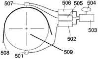
图1示出在基于卷的系统中测试电子印刷的一组代表性组件。基于板的实施例将使用类似的组件,这些组件被部署成测试各个印刷板上而非连续卷上的电子组件。如图1所示,印刷卷3被携带在传输辊5上(也称为传送辊)。如箭头17所指示的,在该图中辊5以及卷3由此逆时针旋转。Figure 1 shows a representative set of components for testing electronic printing in a roll-based system. A board-based embodiment would use similar assemblies deployed to test electronic assemblies on individual printed boards rather than on a continuous roll. As shown in FIG. 1 , the
除用于向用户显示图像的电路(出于清楚的目的在图1中未示出)外,在卷3上印刷各种测试和控制组件。测试和控制组件之间是对准标记7、对准网格线9和测试电路11,该测试电路11包括为测试电路提供电能的第一部分13和生成指示测试电路的至少一个电学性质并由此指示测试电路附近的卷上印刷的电子组件的电学性质的可检测光学信号的第二部分。第一部分13例如可以是印刷光学传感器,诸如光电二极管,而第二部分15例如可以是诸如LED之类的印刷能量发射器。Various test and control components are printed on
在辊5附近安排用于与卷3上印刷的测试和控制组件交互的各种组件。因此,对准传感器19与对准标记7对齐,且对准传感器21与对准网格线9对齐。为了对测试电路11供电,外部能量源23(例如,LED)与第一部分对齐,并且为了读取测试电路生成的测试信息,外部传感器25(例如,光电二极管)与第二部分15对齐。如下所述,在某些实施例中,测试电路在内部生成其自身的功率,从而不使用外部能量源。而且,并非在第二部分15处发射光能,测试电路可产生该部分的光学性质(例如颜色)的变化。在这一情形下,第二部分15通常不会产生光能,因此除外部传感器外,可能期望使光源与第二部分15对齐以帮助检测光学性质,例如用于产生由外部传感器25检测的反射光。Arranged near the
除上述组件外,图1还示出分别通过导线29至35连接至对准传感器19、外部能量源23、外部传感器25、对准传感器21的计算机和信号处理器27的使用。计算机和信号处理器控制这些组件的操作,并接收和分析指示电子印刷工艺的状态的数据。In addition to the components described above, Figure 1 also shows the use of a computer and a
一般而言,如图1所示,测试电路包括利用来自外部光源的光生成电能以运行测试电路的第一区(例如,光伏部分)和测试电路产生由检测器读取的可检测光信号的第二区(读出部分)。尽管已经示出各种可印刷的有机光伏系统且可将其结合本公开使用,但在某些实施例中,可能期望使用常见的材料集和装置结构以产生光伏电源和发射光信号。Generally, as shown in FIG. 1 , a test circuit includes a first region (e.g., a photovoltaic portion) that utilizes light from an external light source to generate electrical energy to operate the test circuit and a test circuit that generates a detectable light signal that is read by a detector. The second area (reading part). Although various printable organic photovoltaic systems have been shown and can be used in conjunction with the present disclosure, in certain embodiments it may be desirable to use common material sets and device structures to generate photovoltaic power and emit light signals.
例如,已经示出包含诸如m-MTDATA和TBADN之类的组合的电荷输运/发射层的装置作为有机发光二极管(OLED)在偏压下发射光,但也作为有机光伏电压(OPV)表现出对UV光的光伏响应。参见Hanzhi Wei、Wenlian Li、Mingtao Li、Wenming Su、Qi Xin、Jinghua Niu、Zhiqiang Zhang、Zhizhi Hu的White organic electroluminescent device with photovoltaic performances(具有光伏性能的白色有机电致发光装置),应用表面科学、第252卷、第6期,2006年1月15日,第2204-2208页。在文献中已经描述了具有类似性能的其它系统。利用这些类型的系统,可构造例如ePaper显示器之类的电子组件以及用于该组件的一个或多个测试电路,而无需引入昂贵的附加工艺步骤或附加材料层。For example, devices containing combined charge transport/emission layers such as m-MTDATA and TBADN have been shown to emit light under bias as organic light-emitting diodes (OLEDs), but also exhibit as organic photovoltaic (OPV) Photovoltaic response to UV light. See Hanzhi Wei, Wenlian Li, Mingtao Li, Wenming Su, Qi Xin, Jinghua Niu, Zhiqiang Zhang, Zhizhi Hu, White organic electroluminescent device with photovoltaic performances, Applied Surface Science, pp. Volume 252, Issue 6, January 15, 2006, Pages 2204-2208. Other systems with similar performance have been described in the literature. With these types of systems, an electronic component such as an ePaper display and one or more test circuits for the component can be constructed without introducing costly additional process steps or additional material layers.
如上所指出的,并非使用发射读出,在一些实施例中,读出的可以是测试电路的区域的光学性质的变化。例如,读出可基于电致变色显示器的颜色。对于发射读出,有可能使基于测试电路的光学性质的变化的读出对附加工艺步骤或附加材料层的需求最小化。例如,在染料敏化太阳能电池装置和电致变色显示器装置中已经采用常见的装置结构,其中装置之间的主要差别是用于光伏吸收或电致变色特性的染料选择。将这种常见的结构连同单个附加印刷步骤(即,用于光伏染料的附加印刷步骤)一起使用能够形成具有光伏电池的印刷基板,该光伏电池可用于制造诊断并且用于为最终装置供电。As noted above, rather than using emission readout, in some embodiments, what is read out may be a change in an optical property of an area of the test circuit. For example, the readout can be based on the color of an electrochromic display. For emission readout, it is possible to minimize the need for additional process steps or additional material layers for readout based on changes in the optical properties of the test circuit. For example, common device structures have been employed in dye-sensitized solar cell devices and electrochromic display devices, where the main difference between devices is the choice of dye for photovoltaic absorption or electrochromic properties. Using this common structure with a single additional printing step (ie, for photovoltaic dyes) enables the formation of printed substrates with photovoltaic cells that can be used to manufacture diagnostics and to power final devices.
为了操作图1的测试电路,沿卷在一个点处将能量注入电路,且在卷的第二点处检测电路对该输入能量的响应。取决于测试电路的结构,可执行各种测试,包括但不限于:(1)确保测试电路正在工作的校准测试;(2)确保电极未开路或短路的连续性测试;(3)测量电极的有效导电能力的线电阻测试;和/或(4)测量电路中的电介质的有效性的电容测试。To operate the test circuit of Figure 1, energy is injected into the circuit at one point along the roll, and the response of the circuit to this input energy is detected at a second point along the roll. Depending on the configuration of the test circuit, various tests can be performed, including but not limited to: (1) a calibration test to ensure that the test circuit is working; (2) a continuity test to ensure that the electrodes are not open or shorted; A wire resistance test for effective electrical conductivity; and/or (4) a capacitance test to measure the effectiveness of the dielectric in the circuit.
具体地,可独立于要测试的电子组件执行校准测试以确保对测试电路的测量的供电和读取是令人满意的。因为通常期望测试电路仅占据基板表面的一小部分,所以接收和发送功能通常需要彼此相邻,且它们之间的实际间隔最小。In particular, calibration testing may be performed independently of the electronic components to be tested to ensure that the powering and reading of measurements of the test circuit is satisfactory. Because the test circuitry is generally expected to occupy only a small portion of the substrate surface, the receive and transmit functions typically need to be adjacent to each other with minimal physical separation between them.
因此,在利用外部光源和发射读出的实施例中,光将被发送至基板上的印刷接收器区(第一部分),且读出区(第二部分)被印刷在附近。当被激活时,接收区将产生操作读出区所必需的能量。如果读出区是OLED装置,则测试通常能够非常快速地完成。如果读出区是电致变色,则输出可能不会完全形成,但是可能存在可被检测到的颜色变化的开始。Thus, in embodiments utilizing an external light source and emission readout, the light will be sent to the printed receiver area (first part) on the substrate, and the readout area (second part) is printed nearby. When activated, the receiving area will generate the energy necessary to operate the reading area. If the readout region is an OLED device, the test can usually be done very quickly. If the readout region is electrochromic, the output may not be fully developed, but there may be the onset of a detectable color change.
供电和读取头的位置和大小一般根据所使用的读出系统的类型而不同。对于OLED系统,读出和供电可同时完成。对于电致变色系统,可能需要更长时间地施加输入功率,需要照明基板上的光电检测器部分一段时间,然后进一步沿卷在读出区轮询数据,以允许电致变色材料改变颜色的时间。在任一情况下,如果OLED装置照明或电致变色装置变色,则校准成功。The location and size of the power supply and readhead generally vary according to the type of readout system used. For OLED systems, reading and powering can be done simultaneously. For electrochromic systems, input power may need to be applied for a longer period of time, requiring illumination of the photodetector portion on the substrate for a period of time, followed by polling data in the readout zone further down the roll to allow time for the electrochromic material to change color . In either case, if the OLED device illuminates or the electrochromic device changes color, the calibration is successful.
连续测试用于确保在典型的印刷线上没有开路。对于该测试,光电检测器供电部分和OLED读出或电致变色读出可与以上关于校准描述的相同,例外是它们现在将由导体的跨度分离。如果导体中有开路,则读出失败。如果响应与校准期间产生的响应相同或基本相同,则导体连续性是可接受的。可沿不同方向放置用于测试连续性的测试电路,且这些测试电路可测试不同的线。所测试的线可以是电子组件的一部分,但通常将是表示电子组件的测试线,而非电子组件的实际部分。Continuity testing is used to ensure there are no opens on a typical printed line. For this test, the photodetector supply section and OLED readout or electrochromic readout can be the same as described above for calibration, with the exception that they will now be separated by a span of conductor. If there is an open circuit in the conductor, the readout will fail. Conductor continuity is acceptable if the response is the same or substantially the same as that produced during calibration. Test circuits for testing continuity can be placed in different directions and can test different lines. The wires being tested may be part of the electronic assembly, but generally will be test wires representing the electronic assembly, not actual parts of the electronic assembly.
通常完成线电阻测试,以确保透明导体电阻不太大。在这种情况下,测试电路包括与连续线串联印刷的电容器。利用光电检测器部分对电路供电,且随后对OLED或电致变色装置供电所需的时间量提供线中电阻量的测量。由于OLED的快速响应时间(其允许系统的激活和去激活被用作与电容器串联的电阻的估计),该测试对于OLED读出是最有效的。A wire resistance test is usually done to ensure that the transparent conductor is not too resistive. In this case, the test circuit includes a capacitor printed in series with the continuous line. Powering the circuit with the photodetector portion and then the amount of time required to power the OLED or electrochromic device provides a measure of the amount of resistance in the line. This test is most efficient for OLED readout due to the fast response time of OLEDs, which allows activation and deactivation of the system to be used as an estimate of the resistance in series with the capacitor.
可通过确定对基板上印刷的电容器的充电和/或放电所需的时间来执行电容测试。如以上的连续性测试那样执行该测试,例外是存在增加的印刷电容器。为了确定电容,可将两种不同长度的导体连接到电容器。OLED的闪烁(充电和放电)频率(或者更精确地,关于闪烁频率)提供对测试电路产品的电阻和电容的估计。确定两种不同线长度的闪烁频率允许获得电容的值。可通过例如在基板上印刷两个光电检测器(一个用于供电一根线而另一个用于供电另一根线)可单独激活两种线长度。Capacitance testing may be performed by determining the time required to charge and/or discharge a capacitor printed on a substrate. This test is performed as the continuity test above, with the exception that there is an added printed capacitor. To determine capacitance, two conductors of different lengths are connected to the capacitor. The blinking (charging and discharging) frequency of the OLED (or, more precisely, about the blinking frequency) provides an estimate of the resistance and capacitance of the test circuit product. Determining the flashing frequency for two different wire lengths allows obtaining the value of the capacitance. Both wire lengths can be activated independently, for example by printing two photodetectors on a substrate, one for powering one wire and the other for powering the other wire.
一旦已知电容,有可能利用等式K=Cd/A确定电容器的电介质材料的介电常数K的值,其中C是电容,d是电介质的厚度,且A是电容器板之一的面积。可利用例如X射线荧光传感器或假设材料的折射率已知则通过光学厚度测量,来确定电介质的厚度。可在不接触基板的情况下利用商业上可购买到的设备执行两种厚度测量。电容测量还可提供有关电介质完整性的信息,即测量可反映电介质中是否存在诸如短路或其它损失源之类的缺陷。Once the capacitance is known, it is possible to determine the value of the dielectric constant K of the capacitor's dielectric material using the equation K=Cd/A, where C is the capacitance, d is the thickness of the dielectric, and A is the area of one of the capacitor plates. The thickness of the dielectric can be determined using, for example, an X-ray fluorescence sensor or by optical thickness measurement assuming the refractive index of the material is known. Both thickness measurements can be performed with commercially available equipment without contacting the substrate. Capacitance measurements also provide information about the integrity of the dielectric, i.e. the measurement reveals the presence of imperfections in the dielectric such as short circuits or other sources of loss.
在图1中,外部LED用于向印刷电路提供激活能量,且内部印刷LED(例如OLED)用于将能量发射回连接到计算机27的外部光电二极管。取代LED,外部能量源可以是半导体激光器。然而,LED通常将是更适合的,因为它们一般比半导体激光器更稳健且更廉价。作为另一替换,可用低能光源替换外部能量源,且将化学能转换成电能的板上电池可被印刷在基板上并用于在测试电路被来自低能源的光激活时对测试电路供电。或者,可构造电池,以便或者在延迟之后或者在被印刷到基板上之后立即自启动。关于外部感测器件,系统的该组件可以是如图1所示的光电二极管、行扫描CCD相机(参见以下)或能够检测光能的另一个电子组件。In FIG. 1 , an external LED is used to provide activation energy to the printed circuit, and an internal printed LED (eg OLED) is used to emit energy back to an external photodiode connected to the
因为非接触测试需要以印刷速度执行且因为一般每个测试需要大量数据,所以系统的检测器部分需要相当快的响应时间。而且,成本总是一个问题,因此在某些实施例中,检测器和信号处理器采用商业上可购买的而非定制的设备。Because non-contact testing needs to be performed at printing speeds and because each test typically requires a large amount of data, the detector portion of the system needs a fairly fast response time. Also, cost is always an issue, so in some embodiments the detectors and signal processors are commercially available rather than custom made.
可用于读取来自测试电路的光响应的检测器(传感器)的类型取决于电路的RC特性。输入到测试电路的能量可具有各种时间波形,其示例包括脉冲函数、一系列定时的开/关脉冲(脉冲串)和正弦波。作为另一替换,可通过输入印刷电路的自然谐振频率的脉冲串并检测谐振输出的幅度来确定电路质量。在这种情况下,外部传感器和相关联的电路可简单地对低幅响应输出0,对可接受的响应输出1。The type of detector (sensor) that can be used to read the light response from the test circuit depends on the RC characteristic of the circuit. The energy input to the test circuit can have various temporal waveforms, examples of which include a pulse function, a timed series of on/off pulses (burst train), and a sine wave. As another alternative, the circuit quality can be determined by inputting a pulse train at the natural resonant frequency of the printed circuit and detecting the magnitude of the resonant output. In this case, the external sensor and associated circuitry can simply output a 0 for a low magnitude response and a 1 for an acceptable response.
外部感测电路测量电路对前述类型输入的响应。具体地,为了提供对印刷电路能力的有效测量,外部传感器必须响应于测试电路的输出发射器的AC组件。一些印刷电路可具有千赫范围的自然谐振,而其它为兆赫范围。为了利用A/D转换器有效地表征这种响应频率,应以高于信号频率两倍的速率量化信号。External sensing circuits measure the circuit's response to the aforementioned types of inputs. Specifically, in order to provide a valid measure of the printed circuit's capabilities, the external sensor must respond to the AC component of the test circuit's output transmitter. Some printed circuits may have a natural resonance in the kilohertz range, while others are in the megahertz range. In order to effectively characterize this response frequency with an A/D converter, the signal should be quantized at a rate higher than twice the signal frequency.
例如,如果电路具有1KHz的自然频率,则约4KHz的数字化速率将适用于精确描绘电路的能力。附连到A/D转换器的光电传感器可利用廉价电子器件容易地在此速率下提供数据。如果使用具有一千个元件的诸如行扫描CCD或接触传感器之类的扫描装置,则设备需要每秒扫描4000次,这将产生总共4MHz的数字化速率。尽管这可利用可获得的设备容易地实现,但将更昂贵。然而,当测试电路的密度高时,这种行扫描是有优势的。For example, if a circuit has a natural frequency of 1KHz, a digitization rate of about 4KHz would be suitable for the ability to accurately describe the circuit. A photosensor attached to an A/D converter can easily provide data at this rate with inexpensive electronics. If a scanning device such as a line scan CCD or contact sensor is used with a thousand elements, the device would need to scan 4000 times per second, which would result in a total digitization rate of 4MHz. While this can be easily accomplished with available equipment, it will be more expensive. However, such line scanning is advantageous when the density of the test circuit is high.
如果测试电路的频率响应约为1MHz而非1KHz,且使用连接至A/D转换器的单个传感器,则可利用商业上可购买的设备再次处理数据。然而,对于一千个元件CCD或接触传感器,数字化速率上升到4GHz,尽管这可实现,但需要昂贵的设备。为了避免这种成本,可使用具有10至50个元件的传感器,以将数据率降低到10至50MHz。利用当前可用的成像系统可容易地管理这种数据率。If the frequency response of the test circuit is around 1 MHz instead of 1 KHz, and a single sensor connected to an A/D converter is used, the data can be reprocessed with commercially available equipment. However, for a thousand element CCD or touch sensor, the digitization rate goes up to 4 GHz, and while this is achievable, it requires expensive equipment. To avoid this cost, sensors with 10 to 50 elements can be used to reduce the data rate to 10 to 50 MHz. Such data rates are readily manageable with currently available imaging systems.
因为测试电路的能量发射器在移动的卷上,所以存在发射器可与外部传感器通信的短的时间窗,并且该窗的长度与移动卷的速度成反比。该时间通信窗指示电路的RC时间测量的另一个极限。Because the energy transmitter of the test circuit is on the moving roll, there is a short window of time during which the transmitter can communicate with the external sensor, and the length of this window is inversely proportional to the speed of the moving roll. This time communication window indicates another limit of the circuit's RC time measurement.
考虑发射器与距离为1mm的外部传感器通信且卷以75mm/秒(3英寸/秒)移动的情况。在这些条件下的通信窗是13毫秒。如果利用1毫秒开和1毫秒关的输入脉冲串激发受测试的电路且这碰巧是电路测量的最优频率,则时间测量窗将仅允许对约6个脉冲的响应的测量。然而,如果利用0.5MHz速率的输入脉冲串激活受测试的电路并且这再次碰巧是电路测试的最优频率,则通信窗将允许来自6000个脉冲的响应的测量。因此能够得出结论:对可进行的测量存在一个较低的频率极限。Consider the case where the transmitter communicates with an external sensor at a distance of 1mm and the roll is moving at 75mm/sec (3 inches/sec). The communication window under these conditions is 13 milliseconds. If the circuit under test is excited with an input pulse train of 1 millisecond on and 1 millisecond off and this happens to be the optimal frequency for circuit measurements, the time measurement window will only allow measurement of the response to about 6 pulses. However, if the circuit under test is activated with an input pulse train at a rate of 0.5 MHz and this again happens to be the optimal frequency for circuit testing, the communication window will allow measurement of the response from 6000 pulses. It can therefore be concluded that there is a lower frequency limit to the measurements that can be made.
这对于低速移动的卷不成问题,因为RC时间常数相对较低,且测试电路的自然谐振频率将大大高于KHz速率。然而,当卷速率增加时,时间通信窗减小,因此需要考虑该限制来设计测试电路。This is not a problem for coils moving at low speeds since the RC time constant is relatively low and the natural resonant frequency of the test circuit will be much higher than the KHz rate. However, when the volume rate increases, the time communication window decreases, so the test circuit needs to be designed considering this limitation.
图2示出其中可采用本文公开的测试方法和装置的典型多站印刷工艺。在该图中,箭头201指示被印刷的卷203的传送方向,且附图标记205、207和209分别表示第一、第二和第三印刷站,其中的每一个包括电子墨盘211、印刷圆柱213、刮墨刀215和压印辊217和干燥器219。Figure 2 illustrates a typical multi-station printing process in which the testing methods and apparatus disclosed herein may be employed. In this figure, an arrow 201 indicates the transport direction of a printed roll 203, and reference numerals 205, 207 and 209 denote first, second and third printing stations, respectively, each of which includes an electronic ink tray 211, printing Cylinder 213, doctor blade 215, embossing roller 217 and dryer 219.
图2的装置可按各种方式操作,包括例如如下。在第一(主)印刷站205中,分立的对准标记(例如,图1中的附图标记7)在印刷圆柱213的每次旋转时被印刷在卷的边缘上一次。该标记充当用于精确检测卷上的第一印刷图案的刻度。在随后的印刷站上的对准传感器(未示出)可检测该标记并向压力控制系统提供第一印刷图案的位置的信息。压力控制系统可使用该信息来相对于第一(主)印刷圆柱调节随后的印刷圆柱的旋转相角。由此,每个随后印刷的层可与第一(主)印刷层精确对准。还可针对每个后续层印刷对准标记(再次参见例如图1中的附图标记)。如果例如层与层对准比与第一(主)层的对准更关键,则这些附加的标记可用于相对于彼此调节后续印刷层。The device of Figure 2 may operate in various ways, including, for example, as follows. In the first (main) printing station 205 discrete alignment marks (eg
除分立的对准标记外,连续的对准网格图案(例如,图1中的附图标记9)也可在第一(主)印刷站处被印刷在卷上。这种网格图案例如可在测试位置处用于检测每个印刷的测试电路的开始。对准传感器(例如,图1中的附图标记21)可向计算机和信号处理器(例如图1中的附图标记27)提供信号,以在印刷的传感器(例如图1中的附图标记13)在其下通过时使外部能量源(例如图1中的附图标记23)通电,由此向测试电路(例如图1中的附图标记11)提供电能。连续的对准网格还可向计算机和信号处理器提供第二信号,以指示它何时利用外部传感器(例如图1中的附图标记25)查找来自印刷能量发射器(例如图1中的附图标记15)的输出信号。此外,该网格图案可用于标记每个测试图案的位置,使得由计算机收集和分析的数据可与沿卷的测试电路的位置相关联。因此可生成“好”和“坏”结果的图,使得与“坏”结果相关联的印刷电子器件随后被丢弃。In addition to discrete alignment marks, a continuous alignment grid pattern (eg
除图1所示的电子测试外,还可针对几何印刷缺陷测试印刷电子电路。例如,可以适当的分辨率光学扫描电子组件,且一系列图像分析规则应用于扫描图像,以查看是否在规定的容限内印刷组件的方位特征,且不包含开路和短路。图3示出利用照明源301和一个或多个相机303(例如,一个或多个CCD相机)进行这种检查的系统,其中当卷305横向穿过传输辊307时所述一个或多个相机303聚焦在卷的一部分上。相机必须通过透镜聚焦在卷的表面上,该透镜的工作距离一般在从6英寸至2或3英尺的范围内,以便从6”至12”视场内收集数据。对于一些应用,在传输(或印刷)辊附近,这种工作距离可能难以适应。In addition to the electronic testing shown in Figure 1, printed electronic circuits can also be tested for geometric printing defects. For example, an electronic component can be optically scanned at an appropriate resolution and a series of image analysis rules applied to the scanned image to see if the orientation characteristics of the printed component are within specified tolerances and free of opens and shorts. FIG. 3 illustrates a system for performing such inspections using an
图4示出解决传输(或印刷)辊附近有限可用空间的问题的系统。该系统使用接触光学传感器401,如图所示其定位成在传输辊403上与卷405邻近。(尽管在商业生产中,该传感器被称为“接触”传感器,如本文所使用的,然而该传感器实际上不接触传输(或印刷)辊。)接触传感器广泛用于桌上扫描仪和传真机,且因此易于以低成本获取。而且它们具有小的覆盖面积,使其能够直接置于辊之上无需消耗大量空间。Figure 4 shows a system that addresses the problem of limited space available near the transfer (or printing) rollers. The system uses a contact optical sensor 401 positioned adjacent to a roll 405 on a transport roller 403 as shown. (Although in commercial production, the sensor is referred to as a "contact" sensor, as used herein, the sensor does not actually touch the transport (or printing) roller.) Contact sensors are widely used in desktop scanners and fax machines , and are therefore readily available at low cost. And they have a small footprint, allowing them to be placed directly on top of the roll without consuming a lot of space.
接触传感器401可由以下构成:(i)传感器线和(ii)将卷的表面聚焦到传感器线上的小梯度指数透镜(GIL)线。接触传感器还可包含光源,例如,一行LED,以照明卷的表面。在尺寸方面,接触传感器可具有小于1英寸×1英寸的横截面,且可放置成距离卷的表面约0.05”。商业上可购买到的装置具有4英寸至10英寸的扫描宽度,且定制设备可覆盖高达20英寸。商业的接触传感器具有200像素/英寸至2400像素/英寸的分辨率。The touch sensor 401 may consist of (i) a sensor wire and (ii) a small gradient index lens (GIL) wire that focuses the surface of the roll onto the sensor wire. The touch sensor may also contain a light source, such as a row of LEDs, to illuminate the surface of the roll. In terms of size, contact sensors can have a cross-section of less than 1 inch by 1 inch and can be placed about 0.05" from the surface of the roll. Commercially available units have scan widths from 4 inches to 10 inches, and custom devices Can cover up to 20". Commercial touch sensors have resolutions from 200 pixels/inch to 2400 pixels/inch.
图5示出集成系统的框图,用于执行(i)用于检测几何印刷缺陷的图像分析和(ii)用于检测电缺陷的测试电路分析。通过使用编码器501、编码器接口502和计算机503,系统首先确定卷速和印刷电路位置。利用该信息、传感器控制器505和照明控制器506来控制接触传感器507的扫描速率,进而控制接触传感器所提供的照明,以维持卷508在传输辊509上的恒定曝光。以此方式产生的卷图像由计算机503处理并解释,且结果被存储在存储介质504中。Figure 5 shows a block diagram of an integrated system for performing (i) image analysis for detecting geometric printing defects and (ii) test circuit analysis for detecting electrical defects. Using the
为了执行电测试,当卷508上的印刷传感器在照明器下通过时,计算机激活接触传感器的照明器。然后在接触传感器的光电二极管处读取来自卷的发射输出,且所得的数据被发送至计算机503用于分析。应注意到,在该实施例和其它实施例中,可通过将不同波长用于外部激发源(例如接触传感器的LED)和印刷测试电路的能量发射器来实现信噪比的大量增加。具体地,可通过将滤波器置于外部传感器之前实现S/N比的这种增加,该滤波器透射具有由测试电路的能量发射器生成的波长的光并阻挡由外部激发源生成的光。To perform the electrical test, the computer activates the illuminators that contact the sensors as the printed sensors on the
表1概括可用于从物理完整性和电学观点上测试印刷电路的各种检测方法。该表按照测试ePaper显示器,应理解,可在用于其它目的的卷和板上印刷的电路上进行本文描述的测试。类似地,表1中列出的传感器、能量源和发射器表示示例性、非限制实施例。Table 1 summarizes various inspection methods that can be used to test printed circuits from a physical integrity and electrical point of view. This table is in accordance with testing ePaper displays, it being understood that the tests described herein can be performed on reels and printed circuits on board for other purposes. Similarly, the sensors, energy sources, and transmitters listed in Table 1 represent exemplary, non-limiting embodiments.
更一般地,本领域的技术人员根据上述公开将清楚不背离本发明的范围和精神的各种修改。以下的权利要求旨在覆盖本文阐述的特定实施例以及这些实施例的修改、变型和等价方案。More generally, various modifications that do not depart from the scope and spirit of the invention will be apparent to those skilled in the art from the above disclosure. The following claims are intended to cover the specific embodiments set forth herein as well as modifications, variations, and equivalents of those embodiments.
表1Table 1

注意:词“外部”指示在ePaper外部的任何装置。Note: the word "external" indicates any device external to ePaper.
词“内部”指示可在ePaper上印刷的任何装置。The word "internal" designates any device that can print on ePaper.
Claims (20)
Applications Claiming Priority (3)
| Application Number | Priority Date | Filing Date | Title |
|---|---|---|---|
| US12/437,779 | 2009-05-08 | ||
| US12/437,779US8378702B2 (en) | 2009-05-08 | 2009-05-08 | Non-contact testing of printed electronics |
| PCT/US2010/033650WO2010129627A2 (en) | 2009-05-08 | 2010-05-05 | Non-contact testing of printed electronics |
Publications (2)
| Publication Number | Publication Date |
|---|---|
| CN102422172Atrue CN102422172A (en) | 2012-04-18 |
| CN102422172B CN102422172B (en) | 2015-11-25 |
Family
ID=43050834
Family Applications (1)
| Application Number | Title | Priority Date | Filing Date |
|---|---|---|---|
| CN201080020891.7AExpired - Fee RelatedCN102422172B (en) | 2009-05-08 | 2010-05-05 | Non-contact testing of printed electronic devices |
Country Status (6)
| Country | Link |
|---|---|
| US (2) | US8378702B2 (en) |
| JP (1) | JP5374639B2 (en) |
| KR (1) | KR101579640B1 (en) |
| CN (1) | CN102422172B (en) |
| TW (1) | TWI428619B (en) |
| WO (1) | WO2010129627A2 (en) |
Cited By (5)
| Publication number | Priority date | Publication date | Assignee | Title |
|---|---|---|---|---|
| CN106707051A (en)* | 2015-11-18 | 2017-05-24 | 四川理工学院 | Electrical property testing device for flexible material |
| CN106796263A (en)* | 2014-10-08 | 2017-05-31 | 伊斯曼柯达公司 | Electrical test system with vision guide alignment |
| CN109375085A (en)* | 2018-09-03 | 2019-02-22 | 中国电子产品可靠性与环境试验研究所((工业和信息化部电子第五研究所)(中国赛宝实验室)) | System and method for health monitoring and early warning of power devices in non-contact board-level circuits |
| CN111337079A (en)* | 2020-03-20 | 2020-06-26 | 深圳市同创鑫电子有限公司 | Test inspection method for printed circuit board production |
| CN115683571A (en)* | 2022-10-31 | 2023-02-03 | 苏州工业园区精泰达自动化有限公司 | Smart watch bright screen factory detection tool |
Families Citing this family (4)
| Publication number | Priority date | Publication date | Assignee | Title |
|---|---|---|---|---|
| AT507322B1 (en)* | 2008-10-07 | 2011-07-15 | Nanoident Technologies Ag | SWITCHING DEVICE FOR ELECTRICAL CONTACT TESTING |
| US8742782B2 (en)* | 2011-07-27 | 2014-06-03 | International Business Machines Corporation | Noncontact electrical testing with optical techniques |
| US10579161B2 (en) | 2014-07-31 | 2020-03-03 | Hewlett-Packard Development Company, L.P. | ION writing calibration |
| US9806828B2 (en) | 2016-02-24 | 2017-10-31 | Frontier Engineering, Llc | Radio frequency generator automated test system |
Citations (7)
| Publication number | Priority date | Publication date | Assignee | Title |
|---|---|---|---|---|
| US6147662A (en)* | 1999-09-10 | 2000-11-14 | Moore North America, Inc. | Radio frequency identification tags and labels |
| US6771807B2 (en)* | 2000-01-18 | 2004-08-03 | Solvision Inc. | Method and system for detecting defects on a printed circuit board |
| US6815973B1 (en)* | 2003-06-13 | 2004-11-09 | Xilinx, Inc. | Optical testing port and wafer level testing without probe cards |
| US6855378B1 (en)* | 1998-08-21 | 2005-02-15 | Sri International | Printing of electronic circuits and components |
| US20070048948A1 (en)* | 2005-08-25 | 2007-03-01 | Accent Optical Technologies, Inc. | Apparatus and method for non-contact assessment of a constituent in semiconductor substrates |
| US20070234918A1 (en)* | 2006-03-31 | 2007-10-11 | Edward Hirahara | System and method for making printed electronic circuits using electrophotography |
| US7301458B2 (en)* | 2005-05-11 | 2007-11-27 | Alien Technology Corporation | Method and apparatus for testing RFID devices |
Family Cites Families (25)
| Publication number | Priority date | Publication date | Assignee | Title |
|---|---|---|---|---|
| US3956698A (en)* | 1974-02-12 | 1976-05-11 | Westinghouse Electric Corporation | Contactless test method for integrated circuits |
| US4820916A (en)* | 1987-05-05 | 1989-04-11 | Simmonds Precision Products | Optically powered sensor system |
| JP2588565B2 (en)* | 1988-02-16 | 1997-03-05 | 富士通株式会社 | Continuity inspection device for printed wiring boards |
| JPH02262071A (en)* | 1989-03-31 | 1990-10-24 | Sekisui Chem Co Ltd | Conduction inspecting method |
| US6156450A (en)* | 1997-07-24 | 2000-12-05 | Eveready Battery Company, Inc. | Battery tester having printed electronic components |
| US6300785B1 (en)* | 1998-10-20 | 2001-10-09 | International Business Machines Corporation | Contact-less probe of semiconductor wafers |
| US6448802B1 (en) | 1998-12-21 | 2002-09-10 | Intel Corporation | Photosensors for testing an integrated circuit |
| TW501293B (en)* | 2001-01-06 | 2002-09-01 | Acer Inc | Method and device to raise the battery efficiency of portable electronic device |
| US6603302B2 (en)* | 2001-08-01 | 2003-08-05 | Frank Joseph Prineppi | Circuit testers |
| US6859031B2 (en)* | 2002-02-01 | 2005-02-22 | Credence Systems Corporation | Apparatus and method for dynamic diagnostic testing of integrated circuits |
| JP2004341216A (en)* | 2003-05-15 | 2004-12-02 | Seiko Epson Corp | ELECTRO-OPTICAL DEVICE SUBSTRATE AND MANUFACTURING METHOD THEREOF, ELECTRO-OPTICAL DEVICE AND ELECTRONIC EQUIPMENT HAVING THE ELECTRO-OPTICAL DEVICE SUBSTRATE |
| US7057409B2 (en) | 2003-12-16 | 2006-06-06 | Texas Instruments Incorporated | Method and apparatus for non-invasively testing integrated circuits |
| US7215133B2 (en) | 2004-01-30 | 2007-05-08 | International Business Machines Corporation | Contactless circuit testing for adaptive wafer processing |
| ES2555309T3 (en)* | 2004-07-06 | 2015-12-30 | Maricare Oy | Sensor product for electric field detection |
| US20060139041A1 (en) | 2004-12-23 | 2006-06-29 | Nystrom Michael J | System and method of testing and utilizing a fluid stream |
| US7202691B2 (en) | 2005-05-31 | 2007-04-10 | Semiconductor Diagnostics, Inc. | Non-contact method for acquiring charge-voltage data on miniature test areas of semiconductor product wafers |
| US20060279297A1 (en) | 2005-06-10 | 2006-12-14 | Nystrom Michael J | Contactless area testing apparatus and method utilizing device switching |
| US20070130490A1 (en)* | 2005-12-02 | 2007-06-07 | Shmuel Silverman | Information protection using properties of a printed electronic circuit |
| DE102006033713A1 (en) | 2006-05-30 | 2007-12-06 | Osram Opto Semiconductors Gmbh | Organic light-emitting component, device with an organic light-emitting component and illumination device, and method for producing an organic light-emitting component |
| KR100844861B1 (en)* | 2006-08-03 | 2008-07-09 | (주) 파루 | A composition for preparing electronic ink and a preparation method thereof |
| JP2008052168A (en)* | 2006-08-28 | 2008-03-06 | Toppan Printing Co Ltd | Manufacturing method of liquid crystal display device |
| US20080084678A1 (en)* | 2006-10-10 | 2008-04-10 | Motorola, Inc. | Printed circuit board and a method for imbedding a battery in a printed circuit board |
| JP2008149311A (en)* | 2006-11-21 | 2008-07-03 | Ricoh Co Ltd | Electronic component manufacturing apparatus, pattern wiring sheet, electronic device sheet and sheet |
| JP2010506196A (en) | 2007-04-17 | 2010-02-25 | オーキンス エレクトロニクス カンパニー,リミテッド | Electro-optic detector |
| JP2009080262A (en)* | 2007-09-26 | 2009-04-16 | Toppan Printing Co Ltd | Electrophoretic display type recording medium and its recorder |
- 2009
- 2009-05-08USUS12/437,779patent/US8378702B2/ennot_activeExpired - Fee Related
- 2010
- 2010-05-05KRKR1020117029382Apatent/KR101579640B1/ennot_activeExpired - Fee Related
- 2010-05-05JPJP2012509934Apatent/JP5374639B2/ennot_activeExpired - Fee Related
- 2010-05-05CNCN201080020891.7Apatent/CN102422172B/ennot_activeExpired - Fee Related
- 2010-05-05WOPCT/US2010/033650patent/WO2010129627A2/enactiveApplication Filing
- 2010-05-07TWTW099114679Apatent/TWI428619B/ennot_activeIP Right Cessation
- 2013
- 2013-01-18USUS13/744,841patent/US9360519B2/ennot_activeExpired - Fee Related
Patent Citations (7)
| Publication number | Priority date | Publication date | Assignee | Title |
|---|---|---|---|---|
| US6855378B1 (en)* | 1998-08-21 | 2005-02-15 | Sri International | Printing of electronic circuits and components |
| US6147662A (en)* | 1999-09-10 | 2000-11-14 | Moore North America, Inc. | Radio frequency identification tags and labels |
| US6771807B2 (en)* | 2000-01-18 | 2004-08-03 | Solvision Inc. | Method and system for detecting defects on a printed circuit board |
| US6815973B1 (en)* | 2003-06-13 | 2004-11-09 | Xilinx, Inc. | Optical testing port and wafer level testing without probe cards |
| US7301458B2 (en)* | 2005-05-11 | 2007-11-27 | Alien Technology Corporation | Method and apparatus for testing RFID devices |
| US20070048948A1 (en)* | 2005-08-25 | 2007-03-01 | Accent Optical Technologies, Inc. | Apparatus and method for non-contact assessment of a constituent in semiconductor substrates |
| US20070234918A1 (en)* | 2006-03-31 | 2007-10-11 | Edward Hirahara | System and method for making printed electronic circuits using electrophotography |
Cited By (6)
| Publication number | Priority date | Publication date | Assignee | Title |
|---|---|---|---|---|
| CN106796263A (en)* | 2014-10-08 | 2017-05-31 | 伊斯曼柯达公司 | Electrical test system with vision guide alignment |
| CN106796263B (en)* | 2014-10-08 | 2019-06-21 | 伊斯曼柯达公司 | Electrical Test System with Vision Guided Alignment |
| CN106707051A (en)* | 2015-11-18 | 2017-05-24 | 四川理工学院 | Electrical property testing device for flexible material |
| CN109375085A (en)* | 2018-09-03 | 2019-02-22 | 中国电子产品可靠性与环境试验研究所((工业和信息化部电子第五研究所)(中国赛宝实验室)) | System and method for health monitoring and early warning of power devices in non-contact board-level circuits |
| CN111337079A (en)* | 2020-03-20 | 2020-06-26 | 深圳市同创鑫电子有限公司 | Test inspection method for printed circuit board production |
| CN115683571A (en)* | 2022-10-31 | 2023-02-03 | 苏州工业园区精泰达自动化有限公司 | Smart watch bright screen factory detection tool |
Also Published As
| Publication number | Publication date |
|---|---|
| US8378702B2 (en) | 2013-02-19 |
| US9360519B2 (en) | 2016-06-07 |
| TW201042274A (en) | 2010-12-01 |
| JP5374639B2 (en) | 2013-12-25 |
| WO2010129627A2 (en) | 2010-11-11 |
| WO2010129627A3 (en) | 2011-02-24 |
| CN102422172B (en) | 2015-11-25 |
| TWI428619B (en) | 2014-03-01 |
| JP2012526284A (en) | 2012-10-25 |
| KR101579640B1 (en) | 2015-12-22 |
| US20100283499A1 (en) | 2010-11-11 |
| KR20120027319A (en) | 2012-03-21 |
| US20130127487A1 (en) | 2013-05-23 |
Similar Documents
| Publication | Publication Date | Title |
|---|---|---|
| CN102422172B (en) | Non-contact testing of printed electronic devices | |
| US9550185B2 (en) | Titer plate with thin-film-light sensor | |
| JP2012083362A (en) | Web inspection module with touch image sensor | |
| JP2004025861A (en) | Medium detecting method for imaging apparatus and system therefor | |
| EP1601599B1 (en) | Optical double feed detection | |
| JP2006078473A5 (en) | ||
| CN103929562B (en) | Imaging sensor, image scanning and thickness detecting method | |
| JP3177347U (en) | Paper quality judgment device | |
| US9927230B2 (en) | Method and apparatus for detecting the fitness for circulation of a value document | |
| SE511822C2 (en) | Device and method for marking defects on a transparent strip | |
| TWI556980B (en) | Systems and methods for detecting substrate alignment during a printing process | |
| WO2015058795A1 (en) | Edge detector | |
| KR101121680B1 (en) | Method and apparatus for providing precise printing using linear encoder | |
| CN103196837A (en) | Image-type device and method for quantitative determination of infrared reflectivity and transmissivity | |
| KR101232890B1 (en) | Method and apparatus for providing precise printing using linear encoder | |
| KR101294358B1 (en) | Method and apparatus for providing precise printing using linear encoder | |
| KR102418949B1 (en) | Apparatus for measuring register and printing system having the same | |
| CN115372249B (en) | A conductive nano polymer film internal damage detection unit and device | |
| KR100853861B1 (en) | Defect Inspection Device and Method of Inkjet PCC Circuit Pattern | |
| CN107690578B (en) | Apparatus and method for sensing | |
| KR20140034571A (en) | Apparatus for inspection of dielectric substance and method for inspection of dielectric substance | |
| TWM434205U (en) | Optical image inspection device |
Legal Events
| Date | Code | Title | Description |
|---|---|---|---|
| C06 | Publication | ||
| PB01 | Publication | ||
| C10 | Entry into substantive examination | ||
| SE01 | Entry into force of request for substantive examination | ||
| C14 | Grant of patent or utility model | ||
| GR01 | Patent grant | ||
| CF01 | Termination of patent right due to non-payment of annual fee | ||
| CF01 | Termination of patent right due to non-payment of annual fee | Granted publication date:20151125 Termination date:20170505 |