CN102420245A - Low voltage trigger silicon controlled rectifier for ESD protection and manufacturing method thereof - Google Patents
Low voltage trigger silicon controlled rectifier for ESD protection and manufacturing method thereofDownload PDFInfo
- Publication number
- CN102420245A CN102420245ACN2010102948829ACN201010294882ACN102420245ACN 102420245 ACN102420245 ACN 102420245ACN 2010102948829 ACN2010102948829 ACN 2010102948829ACN 201010294882 ACN201010294882 ACN 201010294882ACN 102420245 ACN102420245 ACN 102420245A
- Authority
- CN
- China
- Prior art keywords
- doped region
- conductivity type
- type
- esd protection
- low
- Prior art date
- Legal status (The legal status is an assumption and is not a legal conclusion. Google has not performed a legal analysis and makes no representation as to the accuracy of the status listed.)
- Pending
Links
Images


Classifications
- H—ELECTRICITY
- H10—SEMICONDUCTOR DEVICES; ELECTRIC SOLID-STATE DEVICES NOT OTHERWISE PROVIDED FOR
- H10D—INORGANIC ELECTRIC SEMICONDUCTOR DEVICES
- H10D8/00—Diodes
- H10D8/80—PNPN diodes, e.g. Shockley diodes or break-over diodes
Landscapes
- Thyristors (AREA)
- Semiconductor Integrated Circuits (AREA)
Abstract
Description
Translated fromChinese技术领域technical field
本发明属于ESD(Electro-Static discharge,静电释放)防护整流器领域,尤其涉及一种用于ESD防护的低电压触发硅控整流器(low voltage triggering silicon controlled rectifier,LVTSCR)。The invention belongs to the field of ESD (Electro-Static discharge, electrostatic discharge) protection rectifier, in particular to a low voltage triggering silicon controlled rectifier (LVTSCR) for ESD protection.
背景技术Background technique
在先进的CMOS制程中,MOS元件都做有LDD(Lightly Doped Drain,轻掺杂漏区)结构,此LDD结构用来减低MOS之漏极在通道下的电场强度分布,以克服因热载流子效应所造成的I-V特性因长时间漂移的问题。这等效在漏极与源极的两端形成了两个“尖端”,MOS元件很容易因LDD结构做 “尖端放电”而被破坏。从而降低了ESD的防护能力。In the advanced CMOS process, MOS elements are made with LDD (Lightly Doped Drain, lightly doped drain) structure. This LDD structure is used to reduce the electric field intensity distribution of the MOS drain under the channel to overcome the heat-carrying current. The I-V characteristics caused by sub-effects drift for a long time. This is equivalent to forming two "points" at both ends of the drain and source, and the MOS element is easily damaged by the "point discharge" of the LDD structure. Thereby reducing the protection ability of ESD.
在0.35um及以下工艺的CMOS制程中,金属硅化物扩散(silicided diffusion)技术属标准配备。金属硅化物扩散的主要目的是降低MOS元件在漏极与源极的串联杂散电阻,使MOS元件的速度可以有效地提升,因而使CMOS技术可以做到更高频率的应用。但用来做输出级的元件时,由于其串联杂散电阻很小,ESD电流瞬间就因LDD做“尖端放电”而把MOS元件破坏掉了,其ESD防护能力大幅度下滑。In the CMOS process of 0.35um and below, the metal silicide diffusion (silicided diffusion) technology is a standard equipment. The main purpose of the metal silicide diffusion is to reduce the series stray resistance of the MOS element between the drain and the source, so that the speed of the MOS element can be effectively increased, so that the CMOS technology can be applied at a higher frequency. However, when it is used as an output stage component, because the stray resistance in series is very small, the ESD current will instantly destroy the MOS component due to the "point discharge" of the LDD, and its ESD protection ability will drop significantly.
为了克服ESD防护能力下降的问题,发展出了二种制程技术以应用于量产制程中。In order to overcome the problem of decreased ESD protection capability, two process technologies have been developed for mass production.
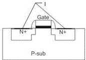
其中一种制程为ESD注入制程 (ESD Implant Process)。如图1所示,为次微米制程下的标准NMOS元件结构,拥有LDD的源极和漏极。在同一CMOS制程中,做出两种不同的NMOS元件,一种具有LDD结构,给内部电路用;另一种不具有LDD结构,如图2所示,给I/O(输入/输出)使用。要把这两种元件结合在同一制程中,便需要在原先的制程中在加入一层ESD注入制程用的光罩(Mask),利用此ESD注入制程光罩(ESD Implant Process Mask)再加上一些额外的制程处理步骤,便可做出不具有LDD结构的NMOS元件。由于用ESD注入制程光罩做出的元件不具有LDD的结构,其结构就像传统的长沟道(Long channel)制程所做出的元件,故其像早期的NMOS元件一样,能拥有较高的ESD防护能力。ESD注入制程的结构图如图2所示,利用ESD注入制程做出来的NMOS元件拥有较深的接面深度,故其有较严重的横向扩散作用,这导致利用ESD注入制程做出的NMOS元件不能用太短的沟道长度。而且用ESD注入制程做的NMOS元件与LDD结构的NMOS元件不同,故需要额外的处理及设计来抽取这种ESD注入制程 NMOS元件的SPICE参数。这种技术无疑增加了制造成本。One of the processes is the ESD implant process (ESD Implant Process). As shown in Figure 1, it is a standard NMOS element structure under the sub-micron process, with the source and drain of LDD. In the same CMOS process, two different NMOS components are made, one has an LDD structure for internal circuits; the other does not have an LDD structure, as shown in Figure 2, for I/O (input/output) use . To combine these two components in the same process, it is necessary to add a layer of mask (Mask) for ESD implantation process in the original process, and use this ESD implantation process mask (ESD Implant Process Mask) plus With some additional process steps, NMOS devices without LDD structure can be made. Since the components made by the ESD injection process mask do not have the LDD structure, its structure is just like the components made by the traditional long channel (Long channel) process, so it can have a higher ESD protection capability. The structural diagram of the ESD implantation process is shown in Figure 2. The NMOS device made by the ESD implantation process has a deeper junction depth, so it has a more serious lateral diffusion effect, which leads to the NMOS device made by the ESD implantation process. Too short a channel length cannot be used. Moreover, the NMOS components made by the ESD injection process are different from the NMOS components of the LDD structure, so additional processing and design are required to extract the SPICE parameters of the NMOS components of the ESD injection process. This technique undoubtedly increases the manufacturing cost.
ESD注入制程是在同一CMOS制程中,做出两种不同的NMOS元件,一种具有LDD结构的NMOS元件,给内部电路用;另一种是不具有LDD结构的NMOS元件,给I/O(输入/输出)用。要把这两种元件结构合并在同一制程中,便需要在原来的制程中加入一层ESD注入制程用的光罩。由于用ESD注入制程光罩做出的元件不具有LDD的结构,故能拥有较高的ESD防护能力。The ESD injection process is to make two different NMOS elements in the same CMOS process, one is an NMOS element with an LDD structure for internal circuits; the other is an NMOS element without an LDD structure for I/O ( input/output) for use. To combine these two device structures in the same process, it is necessary to add a layer of photomask for ESD injection process in the original process. Since the components made by the ESD injection process mask do not have the LDD structure, they can have a higher ESD protection capability.
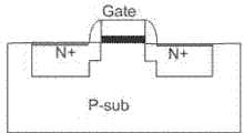
另一种制程为金属硅化物扩散层分隔制程(Silicided —Diffusion Blocking),金属硅化物扩散(silicided diffusion)结构图如图3所示。在金属硅化物扩散层分隔的CMOS制程下,N+扩散(diffusion)的阻值约30—40欧姆/方,但在金属硅化物扩散的先进制程下,其阻值下降到约1—3欧姆/方,当金属硅化物扩散制程的MOS元件被用做输出级的元件时,由于串联杂散电阻都很小,ESD电流很容易便经由焊盘(PAD)传导到MOS元件的LDD结构,一下子就因LDD做“尖端放电”而把MOS元件破坏掉。由于串联杂散电阻可以有效的提升MOS元件对ESD的防护能力,制程上发展出了金属硅化物扩散层分隔制程,其结构有一组实验数据显示,沟道宽度(channel width) W为300um、含LDD结构的NMOS元件在金属硅化物扩散制程下,其HBM(ESD人体模型)的ESD耐压度低于1000V,但若使用金属硅化物扩散层分隔制程技术,在相同的沟道宽度下,其ESD耐压度可提升到约4000V,这显示了金属硅化物扩散层分隔制程用在I/O元件上对ESD防护能力的提升作用。利用金属硅化物扩散层分隔制程消除LDD结构的NMOS元件结构如图4所示,标号1为金属硅化物扩散层分隔区。虽然金属硅化物扩散层分隔制程技术对ESD防护能力有所提升,但除了增加制程复杂度之外,亦会因金属硅化物扩散层的分割处理过程而容易造成污染,这会造NMOS元件低良率的问题。Another process is the metal silicide diffusion layer separation process (Silicided-Diffusion Blocking), and the structure diagram of the metal silicide diffusion (silicided diffusion) is shown in Figure 3. Under the CMOS process separated by the metal silicide diffusion layer, the resistance of N+ diffusion (diffusion) is about 30-40 ohms/square, but under the advanced process of metal silicide diffusion, its resistance drops to about 1-3 ohms/square On the one hand, when the MOS element of the metal silicide diffusion process is used as the element of the output stage, since the series stray resistance is very small, the ESD current is easily conducted to the LDD structure of the MOS element through the pad (PAD), and the The MOS element is destroyed because of the "point discharge" of the LDD. Since the stray resistance in series can effectively improve the ESD protection ability of MOS components, a metal silicide diffusion layer separation process has been developed in the process. A set of experimental data shows that the channel width (channel width) W is 300um, including Under the metal silicide diffusion process, the ESD withstand voltage of the HBM (ESD human body model) of the LDD structure NMOS element is lower than 1000V, but if the metal silicide diffusion layer is used to separate the process technology, under the same channel width, its The ESD withstand voltage can be increased to about 4000V, which shows that the use of the metal silicide diffusion layer separation process on the I/O components can improve the ESD protection capability. The structure of the NMOS element that eliminates the LDD structure by using the metal silicide diffusion layer separation process is shown in FIG. 4 , and the number 1 is the metal silicide diffusion layer separation region. Although the metal silicide diffusion layer separation process technology has improved the ESD protection capability, in addition to increasing the process complexity, it is also easy to cause pollution due to the separation process of the metal silicide diffusion layer, which will cause low yield of NMOS devices. rate problem.
由于较大的串联杂散电阻可以有效的提升MOS元件对ESD的防护能力,金属硅化物扩散层分隔制程为了去除输出极用的NMOS元件中的金属硅化物扩散,使其漏极与源极的串联杂散电阻恢复到30—40欧姆/方的阻值,在制程上需要多用一层光罩来定义出金属硅化物扩散层分隔的区域。Since the larger stray resistance in series can effectively improve the protection ability of MOS elements against ESD, the metal silicide diffusion layer separation process is to remove the metal silicide diffusion in the NMOS element for the output pole, so that the drain and source The series stray resistance is restored to a resistance value of 30-40 ohms/square, and an additional layer of photomask is required in the manufacturing process to define the area separated by the metal silicide diffusion layer.
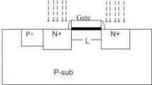
现有技术还提供了一种LVTSCR(Low Voltage Triggering redients Silicon Controlled Rectifier,低电压触发硅控整流器)元件,具有好的ESD防护特性。如图5所示,为SCR(Silicon Controlled Rectifier,硅控整流器)结构。具有P型衬底P-sub、N型阱Nwell、及N+型掺杂半导体区、P+型掺杂半导体区。如图6所示为LVTSCR元件结构,LVTSCR元件是在SCR元件结构中结合了一个浅沟道(short-channel)的NMOS元件构成的,利用一个NMOS的漏极横跨做在N型阱Nwell与P型衬底P-sub的接面上。这可以使SCR元件的起始导通电压下降到等效于浅沟道NMOS元件的聚回崩溃电压,这使得LVTSCR元件不需要额外的第二级ESD防护电路便可以有效的保护内部电路。LVTSCR元件的导通乃是利用其内嵌的浅沟道NMOS元件发生聚回崩溃时,引发电流自其漏极流向P型衬底P-sub,这会引起电流自N型阱N-well流向P型衬底P-sub,因而触发SCR元件的导通,提高了ESD的防护能力。但同时引入了LDD结构,LDD结构做在MOS元件通道的两端,LDD的深度只有约0.02um,这等效在漏极与源极的两端形成了两个“尖端”,“尖端放电”的现象便容易发生在LDD这个尖端结构上,NMOS元件很容易便被ESD所破坏,而降低了ESD的防护能力。The prior art also provides a LVTSCR (Low Voltage Triggering redients Silicon Controlled Rectifier, Low Voltage Triggering Silicon Controlled Rectifier) component, which has good ESD protection characteristics. As shown in Figure 5, it is a SCR (Silicon Controlled Rectifier, silicon-controlled rectifier) structure. It has a P-type substrate P-sub, an N-type well Nwell, an N+ type doped semiconductor region, and a P+ type doped semiconductor region. Figure 6 shows the LVTSCR element structure. The LVTSCR element is composed of a short-channel NMOS element in the SCR element structure. An NMOS drain is used to span the N-type well Nwell and On the junction of the P-substrate P-sub. This can reduce the initial turn-on voltage of the SCR element to the collapse voltage equivalent to that of the shallow channel NMOS element, which makes the LVTSCR element effectively protect the internal circuit without an additional second-level ESD protection circuit. The conduction of the LVTSCR element is based on the collapse of the built-in shallow channel NMOS element, causing the current to flow from the drain to the P-substrate P-sub, which will cause the current to flow from the N-well N-well to the The P-type substrate P-sub triggers the conduction of the SCR element and improves the ESD protection capability. But at the same time, the LDD structure is introduced. The LDD structure is made at both ends of the MOS element channel. The depth of the LDD is only about 0.02um, which is equivalent to forming two "tips" at both ends of the drain and source, "tip discharge" The phenomenon is easy to occur on the cutting-edge structure of LDD, and the NMOS element is easily destroyed by ESD, which reduces the protection ability of ESD.
发明内容Contents of the invention
本发明为解决现有LVTSCR的LDD结构“尖端放电”而导致的ESD防护能力下降的技术问题,在不需要额外增加工艺步骤的情况下,提供一种具有较好ESD防护效果的低电压触发硅控整流器及其制造方法。The present invention solves the technical problem of the decrease of ESD protection capability caused by the "point discharge" of the LDD structure of the existing LVTSCR, and provides a low-voltage trigger silicon with better ESD protection effect without additional process steps. Controlled rectifier and its manufacturing method.
一种用于ESD防护的低电压触发硅控整流器,包括:A low voltage trigger silicon controlled rectifier for ESD protection, comprising:
第一导电型半导体衬底;在所述第一导电型半导体衬底上面设置的第二导电型掺杂阱;在所述第二导电型掺杂阱上设置的第二导电型第一掺杂区和第一导电型第二掺杂区;在所述第一导电型半导体衬底和第二导电型掺杂阱交界处设置的第二导电型第三掺杂区;在第一导电型半导体衬底上还设置了第二导电型第四掺杂区和第一导电型第五掺杂区;第二导电型第三掺杂区和第二导电型第四掺杂区之间设有栅氧化层,栅氧化层上设有多晶硅层;在第二导电型第三掺杂区和栅氧化层之间设有第一场氧结构,在第一导电型半导体衬底和第二导电型掺杂阱上设置将掺杂区隔离开的第二场氧结构;The first conductivity type semiconductor substrate; the second conductivity type doped well arranged on the first conductivity type semiconductor substrate; the second conductivity type first doped well arranged on the second conductivity type doped well region and the second doped region of the first conductivity type; the third doped region of the second conductivity type provided at the junction of the semiconductor substrate of the first conductivity type and the doped well of the second conductivity type; The fourth doped region of the second conductivity type and the fifth doped region of the first conductivity type are also arranged on the substrate; a gate is arranged between the third doped region of the second conductivity type and the fourth doped region of the second conductivity type. An oxide layer, a polysilicon layer is provided on the gate oxide layer; a first field oxygen structure is provided between the third doped region of the second conductivity type and the gate oxide layer, and the semiconductor substrate of the first conductivity type and the doped region of the second conductivity type A second field oxygen structure is set on the heterogeneous well to isolate the doped region;
其中所述第二导电型第一掺杂区和第一导电型第二掺杂区并联于阳极,所述多晶硅层、第二导电型第四掺杂区和第一导电型第五掺杂区并联于阴极。Wherein the first doped region of the second conductivity type and the second doped region of the first conductivity type are connected in parallel to the anode, the polysilicon layer, the fourth doped region of the second conductivity type and the fifth doped region of the first conductivity type connected in parallel to the cathode.
另外,本发明还提供了一种用于ESD防护的低电压触发硅控整流器的制造方法。该方法包括如下步骤:In addition, the invention also provides a manufacturing method of a low-voltage trigger silicon-controlled rectifier for ESD protection. The method comprises the steps of:
A、在第一导电型半导体衬底上注入第二导电型掺杂阱;A. Implanting a second conductivity type doped well on the first conductivity type semiconductor substrate;
B、在所述第二导电型掺杂阱上确定第二导电型第一掺杂区和第一导电型第二掺杂区的位置;在所述第一导电型半导体衬底和第二导电型掺杂阱交界处确定第二导电型第三掺杂区的位置;在所述第一导电型半导体衬底上确定第二导电型第四掺杂区和第一导电型第五掺杂区的位置;确定所述第二导电型第三掺杂区和第二导电型第四掺杂区之间的第一场氧结构区的位置;在所述第一导电型半导体衬底和第二导电型掺杂阱上确定将掺杂区隔离开的第二场氧结构区的位置;B. Determine the positions of the first doped region of the second conductivity type and the second doped region of the first conductivity type on the doped well of the second conductivity type; The position of the third doped region of the second conductivity type is determined at the junction of the type doped well; the fourth doped region of the second conductivity type and the fifth doped region of the first conductivity type are determined on the semiconductor substrate of the first conductivity type position; determine the position of the first field oxygen structure region between the third doped region of the second conductivity type and the fourth doped region of the second conductivity type; between the semiconductor substrate of the first conductivity type and the second Determining the position of the second field oxygen structure region isolating the doped region on the conductive doped well;
C、在第一场氧结构区的位置和第二导电型第四掺杂区的位置之间的第一导电型掺杂半导体衬底上生长栅氧化层,再在栅氧化层上淀积多晶硅;C. Grow a gate oxide layer on the doped semiconductor substrate of the first conductivity type between the position of the first field oxygen structure region and the position of the fourth doped region of the second conductivity type, and then deposit polysilicon on the gate oxide layer ;
D、在第二半导体型第三掺杂区、第二半导体型第四掺杂区的位置上进行轻掺杂漏注入工艺;D. Performing a lightly doped drain implantation process at the positions of the third doped region of the second semiconductor type and the fourth doped region of the second semiconductor type;
E、对第二半导体型第四掺杂区的位置进行侧墙的形成; E. Forming side walls at the position of the fourth doped region of the second semiconductor type;
F、对第二半导体型第一掺杂区、第一半导体型第二掺杂区、第二半导体型第三掺杂区、第二半导体型第四掺杂区、第一半导体型第五掺杂区的位置实施源漏注入工艺。F. For the first doped region of the second semiconductor type, the second doped region of the first semiconductor type, the third doped region of the second semiconductor type, the fourth doped region of the second semiconductor type, and the fifth doped region of the first semiconductor type A source-drain implantation process is implemented at the position of the impurity region.
本发明在低电压触发硅控整流器的第二导电型第三掺杂区与栅氧化层之间加入了第一场氧结构,消除了低电压触发硅控整流器漏极的LDD结构,从而降低了雪崩击穿电压,提高了ESD防护能力。制造该低电压触发硅控整流器时,只需要在确定场氧结构时在N型第三掺杂区和N型第四掺杂区之间加入一个第一场氧结构,不需要额外增加工艺步骤,制成的低电压触发硅控整流器ESD防护能力较强。本发明的低电压触发硅控整流器ESD防护能力强,制造工艺简单,同时在ESD防护过程中功耗较低、发热量小。The present invention adds a first field oxygen structure between the third doped region of the second conductivity type and the gate oxide layer of the low voltage trigger silicon controlled rectifier, eliminating the LDD structure of the drain of the low voltage trigger silicon controlled rectifier, thereby reducing the Avalanche breakdown voltage improves ESD protection. When manufacturing the low-voltage trigger silicon controlled rectifier, it is only necessary to add a first field oxygen structure between the N-type third doped region and the N-type fourth doped region when determining the field oxygen structure, without additional process steps , the manufactured low-voltage trigger silicon controlled rectifier has strong ESD protection capability. The low-voltage trigger silicon-controlled rectifier of the present invention has strong ESD protection capability, simple manufacturing process, low power consumption and low calorific value during the ESD protection process.
附图说明Description of drawings
图1是现有技术提供的带LDD结构的NMOS元件结构图。FIG. 1 is a structural diagram of an NMOS element with an LDD structure provided in the prior art.
图2是现有技术提供的利用ESD注入制程光罩消除LDD结构的NMOS元件结构图。FIG. 2 is a structure diagram of an NMOS element provided in the prior art by using an ESD injection process mask to eliminate an LDD structure.
图3是现有技术提供的在金属硅化物扩散制程下制造的带LDD结构的NMOS元件结构图。FIG. 3 is a structural diagram of an NMOS element with an LDD structure manufactured under a metal silicide diffusion process provided in the prior art.
图4是现有技术提供的在金属硅化物扩散分割制程下消除LDD结构的NMOS元件结构图。FIG. 4 is a structure diagram of an NMOS element in which the LDD structure is eliminated under the metal silicide diffusion division process provided in the prior art.
图5是现有技术提供的硅控整流器结构示意图。Fig. 5 is a schematic structural diagram of a silicon controlled rectifier provided in the prior art.
图6是现有技术提供的低电压触发硅控整流器结构示意图。FIG. 6 is a schematic structural diagram of a low voltage trigger silicon controlled rectifier provided in the prior art.
图7是本发明实施例提供的用于ESD防护的低电压触发硅控整流器结构示意图。FIG. 7 is a schematic structural diagram of a low-voltage trigger silicon-controlled rectifier for ESD protection provided by an embodiment of the present invention.
具体实施方式Detailed ways
为了使本发明所解决的技术问题、技术方案及有益效果更加清楚明白,以下结合附图及实施例,对本发明进行进一步详细说明。应当理解,此处所描述的具体实施例仅仅用以解释本发明,并不用于限定本发明。In order to make the technical problems, technical solutions and beneficial effects solved by the present invention clearer, the present invention will be further described in detail below in conjunction with the accompanying drawings and embodiments. It should be understood that the specific embodiments described here are only used to explain the present invention, not to limit the present invention.
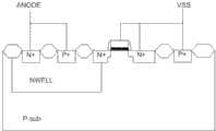
为了解决现有LVTSCR的LDD结构“尖端放电”而导致的ESD防护能力下降的技术问题,本发明提供了一种用于ESD防护的低电压触发硅控整流器。如图7所示,该低电压触发硅控整流器包括:P型掺杂半导体衬底70;在所述P型掺杂半导体衬底70上面设置的N型掺杂阱71;在所述N型掺杂阱71上设置的N型第一掺杂区72和P型第二掺杂区73;在所述P型掺杂半导体衬底70和N型掺杂阱71交界处设置的N型第三掺杂区74;在P型掺杂半导体衬底70上还设置了N型第四掺杂区75和P型第五掺杂区76;N型第三掺杂区74和N型第四掺杂区75之间设有栅氧化层771,栅氧化层上设有多晶硅层772;在N型第三掺杂区74和栅氧化层77之间设有第一场氧结构78,在第一导电型半导体衬底70和第二导电型掺杂阱71上设置将掺杂区隔离开的第二场氧结构79;其中所述N型第一掺杂区72和P型第二掺杂区73并联于阳极,所述多晶硅层772、第四掺杂区75和P型第五掺杂区76并联于阴极。应用时,将阳极接于待被保护电路,阴极接地。In order to solve the technical problem of the decline of ESD protection capability caused by the "point discharge" of the LDD structure of the existing LVTSCR, the present invention provides a low-voltage trigger silicon-controlled rectifier for ESD protection. As shown in FIG. 7 , the low-voltage trigger silicon controlled rectifier includes: a P-type doped semiconductor substrate 70; an N-type doped well 71 arranged on the P-type doped semiconductor substrate 70; The N-type first doped region 72 and the P-type second doped region 73 arranged on the doped well 71; Three doped regions 74; N-type fourth doped regions 75 and P-type fifth doped regions 76 are also set on the P-type doped semiconductor substrate 70; N-type third doped regions 74 and N-type fourth doped regions A gate oxide layer 771 is provided between the doped regions 75, and a polysilicon layer 772 is provided on the gate oxide layer; a first field oxygen structure 78 is provided between the N-type third doped region 74 and the gate oxide layer 77, and in the A second conductive type semiconductor substrate 70 and a second conductive type doped well 71 are provided with a second field oxygen structure 79 isolating the doped regions; wherein the N-type first doped region 72 and the P-type second doped region The region 73 is connected in parallel to the anode, and the polysilicon layer 772 , the fourth doped region 75 and the fifth P-type doped region 76 are connected in parallel to the cathode. In application, connect the anode to the circuit to be protected and the cathode to ground.
上述P型第二掺杂区73的阻值可通过改变制程中的离子掺杂浓度来调整,离子掺杂浓度越低,其阻值越大。其阻值还和P型第二掺杂区73的几何形状相关,例如所述第二掺杂区的掺杂深度D、宽度W或长度L。所述P型第二掺杂区73的长度L和宽度W在设计时即可确定,而等效宽度W’是指接触点A到P型第二掺杂区73边缘的距离。所述等效宽度W’可在硅控整流管的CMOS制程完成后再进行调整。The resistance value of the above-mentioned P-type second doped
本发明在低电压触发硅控整流器的N型第三掺杂区与栅氧化层之间加入了第一场氧结构区,消除了低电压触发硅控整流器漏极的LDD结构,从而降低了雪崩击穿电压,提高了ESD防护能力。The present invention adds a first field oxygen structure region between the N-type third doped region and the gate oxide layer of the low-voltage trigger silicon-controlled rectifier, eliminating the LDD structure of the drain of the low-voltage trigger silicon-controlled rectifier, thereby reducing avalanche breakdown voltage and improved ESD protection.
另外,本发明还提供了一种用于ESD防护的低电压触发硅控整流器的制造方法,包括如下步骤:In addition, the present invention also provides a method for manufacturing a low-voltage trigger silicon-controlled rectifier for ESD protection, including the following steps:
A、在第一导电型半导体衬底上注入第二导电型掺杂阱;A. Implanting a second conductivity type doped well on the first conductivity type semiconductor substrate;
B、在所述第二导电型掺杂阱上确定第二导电型第一掺杂区和第一导电型第二掺杂区的位置;在所述第一导电型半导体衬底和第二导电型掺杂阱交界处确定第二导电型第三掺杂区的位置;在所述第一导电型半导体衬底上确定第二导电型第四掺杂区和第一导电型第五掺杂区的位置;确定所述第二导电型第三掺杂区和第二导电型第四掺杂区之间的第一场氧结构区的位置;在所述第一导电型半导体衬底和第二导电型掺杂阱上确定将掺杂区隔离开的第二场氧结构区的位置;B. Determine the positions of the first doped region of the second conductivity type and the second doped region of the first conductivity type on the doped well of the second conductivity type; The position of the third doped region of the second conductivity type is determined at the junction of the type doped well; the fourth doped region of the second conductivity type and the fifth doped region of the first conductivity type are determined on the semiconductor substrate of the first conductivity type position; determine the position of the first field oxygen structure region between the third doped region of the second conductivity type and the fourth doped region of the second conductivity type; between the semiconductor substrate of the first conductivity type and the second Determining the position of the second field oxygen structure region isolating the doped region on the conductive doped well;
C、在第一场氧结构区的位置和第二导电型第四掺杂区的位置之间的第一导电型掺杂半导体衬底上生长栅氧化层,再在栅氧化层上淀积多晶硅;C. Grow a gate oxide layer on the doped semiconductor substrate of the first conductivity type between the position of the first field oxygen structure region and the position of the fourth doped region of the second conductivity type, and then deposit polysilicon on the gate oxide layer ;
D、在第二半导体型第三掺杂区、第二半导体型第四掺杂区的位置上进行轻掺杂漏注入工艺;D. Performing a lightly doped drain implantation process at the positions of the third doped region of the second semiconductor type and the fourth doped region of the second semiconductor type;
E、对第二半导体型第四掺杂区的位置进行侧墙的形成; E. Forming side walls at the position of the fourth doped region of the second semiconductor type;
F、对第二半导体型第一掺杂区、第一半导体型第二掺杂区、第二半导体型第三掺杂区、第二半导体型第四掺杂区、第一半导体型第五掺杂区的位置实施源漏注入工艺。F. For the first doped region of the second semiconductor type, the second doped region of the first semiconductor type, the third doped region of the second semiconductor type, the fourth doped region of the second semiconductor type, and the fifth doped region of the first semiconductor type A source-drain implantation process is implemented at the position of the impurity region.
进一步的,上述第一导电型为P型,第二导电型为N型。对应的,第一导电型半导体衬底为P型掺杂半导体衬底。第二导电型掺杂阱为N型掺杂阱,第二导电型第一掺杂区、第二导电型第三掺杂区、第二导电型第四掺杂区均为N型掺杂区;第一导电型第二掺杂区、第一导电型第五掺杂区均为P型掺杂区。Further, the above-mentioned first conductivity type is P type, and the second conductivity type is N type. Correspondingly, the semiconductor substrate of the first conductivity type is a P-type doped semiconductor substrate. The doped well of the second conductivity type is an N-type doped well, and the first doped region of the second conductivity type, the third doped region of the second conductivity type, and the fourth doped region of the second conductivity type are all N-type doped regions ; The second doped region of the first conductivity type and the fifth doped region of the first conductivity type are all P-type doped regions.
上述方法在的每个步骤前,均需要涂光刻胶、光刻、清洗,得到所需要的图形。然后进行相应的处理。Before each step of the above method, it is necessary to apply photoresist, photolithography, and cleaning to obtain the required pattern. Then proceed accordingly.
上述步骤D中的轻掺杂注入要比步骤F中的源漏注入时的离子计量少,能量低。注入深度浅,形成低电压触发硅控整流器源极的LDD结构。The light dopant implantation in the above-mentioned step D has less ion metering and lower energy than the source-drain implantation in the step F. The implantation depth is shallow to form the LDD structure of the source of the silicon controlled rectifier triggered by low voltage.
步骤E中对N型第四掺杂区进行侧墙的形成;侧墙用来环绕多晶硅栅,防止更大剂量的源漏注入过于接近沟道以致可能发生源漏穿通。In step E, sidewalls are formed on the N-type fourth doped region; the sidewalls are used to surround the polysilicon gate to prevent source-drain implantation of a larger dose from being too close to the channel so that source-drain punch-through may occur.
该方法在确定场氧结构时在N型第三掺杂区和N型第四掺杂区之间加入一个第一场氧结构,不需要额外增加工艺步骤,但制造出的低电压触发硅控整流器的没有LDD结构,从而提高了低电压触发硅控整流器的ESD防护能力。In this method, a first field oxygen structure is added between the N-type third doped region and the N-type fourth doped region when determining the field oxygen structure, which does not require additional process steps, but the manufactured low-voltage trigger silicon control The rectifier does not have an LDD structure, thereby improving the ESD protection capability of the low voltage triggered silicon controlled rectifier.
以上所述仅为本发明的较佳实施例而已,并不用以限制本发明,凡在本发明的精神和原则之内所作的任何修改、等同替换和改进等,均应包含在本发明的保护范围之内。 The above descriptions are only preferred embodiments of the present invention, and are not intended to limit the present invention. Any modifications, equivalent replacements and improvements made within the spirit and principles of the present invention should be included in the protection of the present invention. within range. the
Claims (8)
Priority Applications (1)
| Application Number | Priority Date | Filing Date | Title |
|---|---|---|---|
| CN2010102948829ACN102420245A (en) | 2010-09-28 | 2010-09-28 | Low voltage trigger silicon controlled rectifier for ESD protection and manufacturing method thereof |
Applications Claiming Priority (1)
| Application Number | Priority Date | Filing Date | Title |
|---|---|---|---|
| CN2010102948829ACN102420245A (en) | 2010-09-28 | 2010-09-28 | Low voltage trigger silicon controlled rectifier for ESD protection and manufacturing method thereof |
Publications (1)
| Publication Number | Publication Date |
|---|---|
| CN102420245Atrue CN102420245A (en) | 2012-04-18 |
Family
ID=45944556
Family Applications (1)
| Application Number | Title | Priority Date | Filing Date |
|---|---|---|---|
| CN2010102948829APendingCN102420245A (en) | 2010-09-28 | 2010-09-28 | Low voltage trigger silicon controlled rectifier for ESD protection and manufacturing method thereof |
Country Status (1)
| Country | Link |
|---|---|
| CN (1) | CN102420245A (en) |
Cited By (4)
| Publication number | Priority date | Publication date | Assignee | Title |
|---|---|---|---|---|
| CN102856323A (en)* | 2012-09-14 | 2013-01-02 | 浙江大学 | Transient voltage suppressor and application thereof |
| CN103378087A (en)* | 2012-04-28 | 2013-10-30 | 无锡华润上华半导体有限公司 | Electrostatic discharge protection structure and manufacturing method thereof |
| CN114927574A (en)* | 2022-05-24 | 2022-08-19 | 上海晶岳电子有限公司 | Structure of vertical structure VDMOS (vertical double-diffused metal oxide semiconductor) process LVTSCR (Low Voltage thyristor controlled rectifier) device and manufacturing method thereof |
| CN117096153A (en)* | 2023-10-18 | 2023-11-21 | 荣湃半导体(上海)有限公司 | ESD integrated MOSFET device and preparation method thereof |
Citations (5)
| Publication number | Priority date | Publication date | Assignee | Title |
|---|---|---|---|---|
| US5225702A (en)* | 1991-12-05 | 1993-07-06 | Texas Instruments Incorporated | Silicon controlled rectifier structure for electrostatic discharge protection |
| CN1354516A (en)* | 2000-11-16 | 2002-06-19 | 世界先进积体电路股份有限公司 | Electrostatic discharge protection components and related circuits |
| CN1437258A (en)* | 2002-02-09 | 2003-08-20 | 台湾积体电路制造股份有限公司 | Antistatic assembly and antistatic circuit for electrostatic discharge protection assembly |
| CN1913174A (en)* | 2005-08-09 | 2007-02-14 | 台湾积体电路制造股份有限公司 | Semiconductor device and high voltage P-type metal oxide semiconductor device |
| CN101740392A (en)* | 2008-11-27 | 2010-06-16 | 中芯国际集成电路制造(上海)有限公司 | LDMOS (Laterally Diffused Metal Oxide Semiconductor) transistor, semiconductor device and manufacture method thereof |
- 2010
- 2010-09-28CNCN2010102948829Apatent/CN102420245A/enactivePending
Patent Citations (5)
| Publication number | Priority date | Publication date | Assignee | Title |
|---|---|---|---|---|
| US5225702A (en)* | 1991-12-05 | 1993-07-06 | Texas Instruments Incorporated | Silicon controlled rectifier structure for electrostatic discharge protection |
| CN1354516A (en)* | 2000-11-16 | 2002-06-19 | 世界先进积体电路股份有限公司 | Electrostatic discharge protection components and related circuits |
| CN1437258A (en)* | 2002-02-09 | 2003-08-20 | 台湾积体电路制造股份有限公司 | Antistatic assembly and antistatic circuit for electrostatic discharge protection assembly |
| CN1913174A (en)* | 2005-08-09 | 2007-02-14 | 台湾积体电路制造股份有限公司 | Semiconductor device and high voltage P-type metal oxide semiconductor device |
| CN101740392A (en)* | 2008-11-27 | 2010-06-16 | 中芯国际集成电路制造(上海)有限公司 | LDMOS (Laterally Diffused Metal Oxide Semiconductor) transistor, semiconductor device and manufacture method thereof |
Non-Patent Citations (1)
| Title |
|---|
| 伍国珏: "《半导体器件完全指南》", 31 July 2009* |
Cited By (8)
| Publication number | Priority date | Publication date | Assignee | Title |
|---|---|---|---|---|
| CN103378087A (en)* | 2012-04-28 | 2013-10-30 | 无锡华润上华半导体有限公司 | Electrostatic discharge protection structure and manufacturing method thereof |
| WO2013159746A1 (en)* | 2012-04-28 | 2013-10-31 | 无锡华润上华半导体有限公司 | Electrostatic discharge protection structure and fabrication method therefor |
| EP2717317A4 (en)* | 2012-04-28 | 2014-12-03 | Csmc Technologies Fab1 Co Ltd | ELECTROSTATIC DISCHARGE PROTECTION STRUCTURE AND METHOD OF MANUFACTURING THE SAME |
| CN103378087B (en)* | 2012-04-28 | 2016-02-24 | 无锡华润上华半导体有限公司 | Electrostatic discharge protection structure and manufacture method thereof |
| CN102856323A (en)* | 2012-09-14 | 2013-01-02 | 浙江大学 | Transient voltage suppressor and application thereof |
| CN114927574A (en)* | 2022-05-24 | 2022-08-19 | 上海晶岳电子有限公司 | Structure of vertical structure VDMOS (vertical double-diffused metal oxide semiconductor) process LVTSCR (Low Voltage thyristor controlled rectifier) device and manufacturing method thereof |
| CN117096153A (en)* | 2023-10-18 | 2023-11-21 | 荣湃半导体(上海)有限公司 | ESD integrated MOSFET device and preparation method thereof |
| CN117096153B (en)* | 2023-10-18 | 2024-01-19 | 荣湃半导体(上海)有限公司 | ESD-integrated MOSFET device and preparation method thereof |
Similar Documents
| Publication | Publication Date | Title |
|---|---|---|
| CN104752417B (en) | Controllable silicon electrostatic protection device and forming method thereof | |
| CN102969312B (en) | High-voltage ESD (electro-static discharge) protective device triggered by bidirectional substrate | |
| CN101630683B (en) | Integrated electrostatic discharge device | |
| CN107437563B (en) | LDMOS transistor and forming method thereof, and ESD device and forming method thereof | |
| CN100583429C (en) | PMOS pipe built-in bidirectional thyristor electrostatic protection device | |
| CN110649016B (en) | Silicon controlled rectifier type ESD (electro-static discharge) protection structure without hysteresis effect and implementation method thereof | |
| CN104716132B (en) | The thyristor and its circuit of a kind of low trigger voltage and high maintenance voltage | |
| US20210358903A1 (en) | TVS Device And Manufacturing Method Therefor | |
| CN203071072U (en) | High-voltage ESD (electro-static discharge) protective device triggered by bidirectional substrate | |
| CN106653856A (en) | VDMOS device capable of resisting single event burnout and manufacturing method of VDMOS device | |
| CN115274652A (en) | An enhanced high robustness thyristor electrostatic protection device and its manufacturing method | |
| JP7642100B2 (en) | GGNMOS TRANSISTOR STRUCTURE, ESD PROTECTION DEVICE AND CIRCUIT | |
| CN108321188A (en) | Insulated gate bipolar transistor and forming method thereof | |
| CN102420245A (en) | Low voltage trigger silicon controlled rectifier for ESD protection and manufacturing method thereof | |
| CN107346786B (en) | GGNMOS transistors, multi-finger GGNMOS devices and circuits | |
| CN113764401A (en) | A kind of asymmetric band gate triac electrostatic protection device and manufacturing method thereof | |
| CN108389857B (en) | Polysilicon dummy gate electrostatic discharge device for improving holding voltage and manufacturing method thereof | |
| CN101697355A (en) | A uniform trigger semiconductor silicon controlled rectifier controller for ESD | |
| CN104124275A (en) | Square-concentric multi-fork field effect transistor and manufacturing method thereof | |
| CN106711209A (en) | A Novel VSCR Device for ESD Protection | |
| CN102280382A (en) | Electrostatic discharge protecting structure integrated in insulated gate bipolar transistor (IGBT) apparatus and manufacturing method of electrostatic discharge protecting structure | |
| CN112928113B (en) | A tunneling current triggered SCR device | |
| CN106298777B (en) | A GGNMOS device used as ESD protection and its manufacturing method | |
| WO2023098174A1 (en) | Electrostatic discharge protection structure | |
| CN103794650B (en) | Depletion type power MOS device integrating ESD protection and manufacturing method thereof |
Legal Events
| Date | Code | Title | Description |
|---|---|---|---|
| C06 | Publication | ||
| PB01 | Publication | ||
| C10 | Entry into substantive examination | ||
| SE01 | Entry into force of request for substantive examination | ||
| C12 | Rejection of a patent application after its publication | ||
| RJ01 | Rejection of invention patent application after publication | Application publication date:20120418 |