CN102414957A - Wireless power transmission system - Google Patents
Wireless power transmission systemDownload PDFInfo
- Publication number
- CN102414957A CN102414957ACN201180001906XACN201180001906ACN102414957ACN 102414957 ACN102414957 ACN 102414957ACN 201180001906X ACN201180001906X ACN 201180001906XACN 201180001906 ACN201180001906 ACN 201180001906ACN 102414957 ACN102414957 ACN 102414957A
- Authority
- CN
- China
- Prior art keywords
- wiring
- transmission system
- power transmission
- wireless power
- lead
- Prior art date
- Legal status (The legal status is an assumption and is not a legal conclusion. Google has not performed a legal analysis and makes no representation as to the accuracy of the status listed.)
- Granted
Links
Images


Classifications
- H—ELECTRICITY
- H01—ELECTRIC ELEMENTS
- H01F—MAGNETS; INDUCTANCES; TRANSFORMERS; SELECTION OF MATERIALS FOR THEIR MAGNETIC PROPERTIES
- H01F38/00—Adaptations of transformers or inductances for specific applications or functions
- H01F38/14—Inductive couplings
- H—ELECTRICITY
- H01—ELECTRIC ELEMENTS
- H01F—MAGNETS; INDUCTANCES; TRANSFORMERS; SELECTION OF MATERIALS FOR THEIR MAGNETIC PROPERTIES
- H01F21/00—Variable inductances or transformers of the signal type
- H—ELECTRICITY
- H02—GENERATION; CONVERSION OR DISTRIBUTION OF ELECTRIC POWER
- H02J—CIRCUIT ARRANGEMENTS OR SYSTEMS FOR SUPPLYING OR DISTRIBUTING ELECTRIC POWER; SYSTEMS FOR STORING ELECTRIC ENERGY
- H02J50/00—Circuit arrangements or systems for wireless supply or distribution of electric power
- H02J50/10—Circuit arrangements or systems for wireless supply or distribution of electric power using inductive coupling
- H02J50/12—Circuit arrangements or systems for wireless supply or distribution of electric power using inductive coupling of the resonant type
- H—ELECTRICITY
- H01—ELECTRIC ELEMENTS
- H01F—MAGNETS; INDUCTANCES; TRANSFORMERS; SELECTION OF MATERIALS FOR THEIR MAGNETIC PROPERTIES
- H01F21/00—Variable inductances or transformers of the signal type
- H01F21/12—Variable inductances or transformers of the signal type discontinuously variable, e.g. tapped
- H—ELECTRICITY
- H02—GENERATION; CONVERSION OR DISTRIBUTION OF ELECTRIC POWER
- H02M—APPARATUS FOR CONVERSION BETWEEN AC AND AC, BETWEEN AC AND DC, OR BETWEEN DC AND DC, AND FOR USE WITH MAINS OR SIMILAR POWER SUPPLY SYSTEMS; CONVERSION OF DC OR AC INPUT POWER INTO SURGE OUTPUT POWER; CONTROL OR REGULATION THEREOF
- H02M7/00—Conversion of AC power input into DC power output; Conversion of DC power input into AC power output
- H02M7/42—Conversion of DC power input into AC power output without possibility of reversal
- H02M7/44—Conversion of DC power input into AC power output without possibility of reversal by static converters
- H02M7/48—Conversion of DC power input into AC power output without possibility of reversal by static converters using discharge tubes with control electrode or semiconductor devices with control electrode
- H02M7/4815—Resonant converters
- H02M7/4818—Resonant converters with means for adaptation of resonance frequency, e.g. by modification of capacitance or inductance of resonance circuits
- Y—GENERAL TAGGING OF NEW TECHNOLOGICAL DEVELOPMENTS; GENERAL TAGGING OF CROSS-SECTIONAL TECHNOLOGIES SPANNING OVER SEVERAL SECTIONS OF THE IPC; TECHNICAL SUBJECTS COVERED BY FORMER USPC CROSS-REFERENCE ART COLLECTIONS [XRACs] AND DIGESTS
- Y02—TECHNOLOGIES OR APPLICATIONS FOR MITIGATION OR ADAPTATION AGAINST CLIMATE CHANGE
- Y02B—CLIMATE CHANGE MITIGATION TECHNOLOGIES RELATED TO BUILDINGS, e.g. HOUSING, HOUSE APPLIANCES OR RELATED END-USER APPLICATIONS
- Y02B70/00—Technologies for an efficient end-user side electric power management and consumption
- Y02B70/10—Technologies improving the efficiency by using switched-mode power supplies [SMPS], i.e. efficient power electronics conversion e.g. power factor correction or reduction of losses in power supplies or efficient standby modes
Landscapes
- Engineering & Computer Science (AREA)
- Power Engineering (AREA)
- Computer Networks & Wireless Communication (AREA)
- Charge And Discharge Circuits For Batteries Or The Like (AREA)
Abstract
Translated fromChinese
Description
Translated fromChinese技术领域technical field
本发明涉及以非接触的方式进行充电供电或电力收集的无线电力传输系统以及用于该系统中的无线电力传输装置。The present invention relates to a wireless power transmission system for performing charging and power supply or power collection in a non-contact manner, and a wireless power transmission device used in the system.
背景技术Background technique
在电子设备的移动性确保对策/电子设备的防水对策、壁挂式电视机的无布线化、简便地向电动汽车等大型设备充电供电方面,高度关注无接点/非接触方式的能量充电供电技术。In terms of measures to ensure the mobility of electronic equipment, waterproof measures for electronic equipment, wiring-free wall-mounted TVs, and easy charging and power supply of large-scale equipment such as electric vehicles, attention is paid to non-contact/non-contact energy charging and power supply technologies.
作为非接触的电力传输方式,不仅仅是以往一直研究的电磁感应方式,还提出专利文献1所记载的磁谐振方式。认为这种磁谐振利用谐振天线间的谐振模式间耦合,能够实现距离比以往的电磁感应方式更长、效率更高的电力传输,尤其是若利用谐振磁场,则与利用谐振电场的情形相比,可以回避对周边生物体带来的影响。As a non-contact power transmission method, not only the electromagnetic induction method that has been studied conventionally, but also the magnetic resonance method described in Patent Document 1 has been proposed. It is believed that this type of magnetic resonance utilizes the inter-resonance mode coupling between resonant antennas, and it is possible to realize power transmission over a longer distance and with higher efficiency than conventional electromagnetic induction methods. , can avoid the impact on surrounding organisms.
若对磁谐振方式进一步描述详细内容,则如专利文献1的说明书中的段落【0033】所记载的,谐振器也可以利用两端开放的环状线圈固有的自谐振现象。再有,如段落【0038】所记载的,也可以是装载了电容的线圈。磁谐振方式的电力传输系统可以看作是通过采用耦合系数不为1的高Q电路而提高了传输效率的电磁感应系统。其中,因为耦合系数低(k≠1),所以与被设定为k≈1的电磁感应相比,产生以下限制:仅在保证了送电器与送电谐振器、受电器与受电谐振器间的阻抗匹配的状态下才能产生高效率传输。If the details of the magnetic resonance method are further described, as described in paragraph [0033] in the specification of Patent Document 1, the resonator can also utilize the inherent self-resonance phenomenon of a loop coil with both ends open. In addition, as described in the paragraph [0038], it may be a coil loaded with a capacitor. The power transmission system of the magnetic resonance method can be regarded as an electromagnetic induction system in which the transmission efficiency is improved by using a high-Q circuit whose coupling coefficient is not 1. Among them, since the coupling coefficient is low (k≠1), compared with the electromagnetic induction set to k≈1, the following limitation occurs: Only when the power transmitter and the power transmitting resonator, the power receiver and the power receiving resonator High-efficiency transmission can only be produced under the state of impedance matching between them.
另一方面,除了以恒流模式工作的光器件等一部分器件以外,大多是被恒压驱动的电子器件、电子设备。再有,家庭用插座等或太阳能电池、燃料电池等成为电源的电路也大多提供接近于恒定的电压。因此,若磁谐振方式的能量传输系统可以实现向阻抗变动的对应,则能够在更多的电源或更多的负载中采用本系统。因此,虽然送电模块或受电模块也优选发现阻抗变动对应功能,但尤其是构成为至少包含谐振器对的无线部需要发现可变功能。作为可变功能,需要兼顾向阻抗变动的对应和高效率传输特性的维持。On the other hand, except for some devices such as optical devices that operate in a constant current mode, most of them are electronic devices and electronic equipment that are driven by a constant voltage. Furthermore, circuits that serve as power sources such as household sockets, solar cells, fuel cells, etc. also provide a nearly constant voltage in many cases. Therefore, if the energy transmission system of the magnetic resonance system can respond to impedance fluctuations, this system can be used for more power sources or more loads. Therefore, although it is preferable for the power transmitting module or the power receiving module to find a function corresponding to impedance variation, it is particularly necessary for a wireless unit configured to include at least a pair of resonators to find a variable function. As a variable function, it is necessary to balance the response to impedance fluctuations and the maintenance of high-efficiency transmission characteristics.
专利文献2中公开了可变电感器的构成例。Patent Document 2 discloses a configuration example of a variable inductor.
再有,专利文献3中公开了可变谐振器的构成,即:从并联配置的不同容量的电容器组中选择与电感器连接的电容器,以获得可变谐振频率特性。Furthermore, Patent Document 3 discloses a configuration of a variable resonator in which a capacitor connected to an inductor is selected from capacitor banks of different capacities arranged in parallel to obtain a variable resonance frequency characteristic.
(先行技术文献)(Prior Art Literature)
专利文献1:美国申请公开2008/0278264-A1公报(图6、图31)Patent Document 1: U.S. Application Publication No. 2008/0278264-A1 (FIG. 6, FIG. 31)
专利文献2:JP特开2007-142418号公报(图3)Patent Document 2: JP Unexamined Publication No. 2007-142418 (FIG. 3)
专利文献3:JP特开2001-344574号公报(图3)Patent Document 3: JP Unexamined Publication No. 2001-344574 (FIG. 3)
发明内容Contents of the invention
(发明想要解决的课题)(The problem that the invention wants to solve)
在本发明中解决以下课题:向磁谐振方式的无线电力传输系统导入在构成内包含可变电感器电路的可变谐振器来实现与多个动作条件对应之际所产生的将传输效率继续维持较高值的难度、为了回避该困难而需要增大布线总量。The present invention solves the problem of introducing a variable resonator including a variable inductor circuit into a magnetic resonance type wireless power transmission system to achieve continuous transmission efficiency that occurs when responding to a plurality of operating conditions. It is difficult to maintain a high value, and in order to avoid this difficulty, it is necessary to increase the total amount of wiring.
(用于解决课题的手段)(means to solve the problem)
本发明是为了解决上述现有的课题而完成的,其目的在于提供一种不会使布线总量无故增大、且即使在多个切换状态下也能维持高的传输效率的无线电力传输系统。The present invention was made to solve the above-mentioned conventional problems, and an object of the present invention is to provide a wireless power transmission system that can maintain high transmission efficiency even in a plurality of switching states without increasing the total amount of wiring unnecessarily. .
本发明的无线电力传输系统具备送电谐振器及受电谐振器,且经由谐振磁场而以非接触的方式传输电力,其中,所述送电谐振器及所述受电谐振器的至少一方是串联谐振电路,所述串联谐振电路包括:电感器,其包括螺线布线、用于将所述螺线布线的第一连接点连接到供电结构的第一引线、用于将所述螺线布线的不同于所述第一连接点的第二连接点连接到所述供电结构的第二引线、和用于将所述螺线布线的比所述第二连接点更远离所述第一连接点的第三连接点连接到所述供电结构的第三引线;分别与所述第二引线及第三引线连接的多个开关;以及多个电容,经由所述多个开关中的对应的开关而分别与所述第二引线及第三引线串联连接;所述串联谐振电路能够随着通过所述多个开关中的选择性导通的开关所选择的电流路径而具有不同的电感值,所述多个电容的电容值被设定为:不依赖于选择性导通的开关,所述串联谐振电路的谐振频率表示恒定的值;所述螺线布线在从所述第二连接点到所述第一连接点为止的范围内,具有所述谐振频率下的每单位长度的布线电阻被设定得比所述螺线布线的其他范围的至少一部分还低的低电阻部分。The wireless power transmission system of the present invention includes a power transmitting resonator and a power receiving resonator, and transmits electric power in a non-contact manner via a resonant magnetic field, wherein at least one of the power transmitting resonator and the power receiving resonator is a series resonant circuit comprising: an inductor comprising a spiral wiring, a first lead for connecting a first connection point of the spiral wiring to a power supply structure, a first lead for connecting the spiral wiring A second connection point different from the first connection point is connected to a second lead of the power supply structure, and a second connection point for routing the spiral is farther from the first connection point than the second connection point The third connection point of the power supply structure is connected to the third lead of the power supply structure; a plurality of switches respectively connected to the second lead and the third lead; and a plurality of capacitors are connected via corresponding switches in the plurality of switches. respectively connected in series with the second lead and the third lead; the series resonant circuit can have different inductance values according to the current path selected by the selectively conductive switch among the plurality of switches, the Capacitance values of the plurality of capacitors are set such that the resonant frequency of the series resonant circuit represents a constant value regardless of the selectively conductive switches; In the range up to the first connection point, there is a low-resistance portion in which the wiring resistance per unit length at the resonance frequency is set lower than at least a part of other ranges of the spiral wiring.
在优选的实施方式中,所述低电阻部分在所述谐振频率下的每单位长度的布线电阻比其他部分在所述谐振频率下的每单位长度的布线电阻还低。In a preferred embodiment, the wiring resistance per unit length of the low-resistance portion at the resonance frequency is lower than the wiring resistance per unit length of the other portions at the resonance frequency.
在优选的实施方式中,所述谐振频率下的所述螺线布线的布线电阻的、从所述第二连接点到所述第一连接点为止的整个范围的平均值比所述谐振频率下的所述螺线布线的布线电阻在所述范围外的平均值还低。In a preferred embodiment, the average value of the wiring resistance of the spiral wiring at the resonance frequency over the entire range from the second connection point to the first connection point is lower than the resonance frequency. The average value of the wiring resistance of the spiral wiring outside the range is low.
在优选的实施方式中,所述螺线布线的所述低电阻部分具有根数比其他部分还多的多根布线并列配置的结构。In a preferred embodiment, the low-resistance portion of the spiral wiring has a structure in which a larger number of wirings are arranged in parallel than other portions.
在优选的实施方式中,所述螺线布线的所述低电阻部分包含直径比其他部分还大的至少1根布线。In a preferred embodiment, the low-resistance portion of the spiral wiring includes at least one wiring having a larger diameter than other portions.
在优选的实施方式中,所述螺线布线的所述低电阻部分包含厚度比其他部分还小的至少1根布线。In a preferred embodiment, the low-resistance portion of the spiral wiring includes at least one wiring whose thickness is smaller than that of other portions.
在优选的实施方式中,所述螺线布线的所述低电阻部分包含宽度比其他部分还宽的至少1根布线。In a preferred embodiment, the low-resistance portion of the spiral wiring includes at least one wiring wider than other portions.
在优选的实施方式中,所述电感器包含第四引线,其用于将所述螺线布线的比所述第一连接点更远离所述第二连接点的第四连接点连接到所述供电结构,所述第一引线及所述第四引线分别通过与所述多个开关不同的多个开关被选择性地连接到所述供电结构。In a preferred embodiment, the inductor comprises a fourth lead for connecting a fourth connection point of the spiral wiring farther from the second connection point than the first connection point to the A power supply structure, the first lead and the fourth lead are selectively connected to the power supply structure through a plurality of switches different from the plurality of switches, respectively.
在优选的实施方式中,具有所述串联谐振电路所能具备的多个电感值中的最低电感值时成为所述螺线布线的电流路径的部分位于螺线结构的最内周侧。In a preferred embodiment, when the series resonant circuit has the lowest inductance value among a plurality of inductance values that the series resonant circuit can have, the portion that becomes the current path of the spiral wiring is located on the innermost peripheral side of the spiral structure.
在优选的实施方式中,所述多个开关的额定值或构成开关的晶体管的栅极宽度随着在导通时流经开关的电流而具有不同的值。In a preferred embodiment, the ratings of the plurality of switches or the gate widths of transistors constituting the switches have different values depending on the current flowing through the switches when they are turned on.
在优选的实施方式中,所述多个开关中,导通时流过的电流更多的开关的额定值或构成开关的晶体管的栅极宽度比导通时流经的电流更少的开关的额定值或构成开关的晶体管的栅极宽度还大。In a preferred embodiment, among the plurality of switches, the rated value of the switch whose current flows when turned on or the gate width of the transistor constituting the switch is smaller than that of the switch whose current flows when turned on. The rating or the gate width of the transistors that make up the switch is also larger.
在优选的实施方式中,在所述串联谐振电路不参与电力传输时,通过控制所述多个开关,从而使所述谐振频率变化为不同的值。In a preferred embodiment, when the series resonant circuit does not participate in power transmission, the resonant frequency is changed to different values by controlling the plurality of switches.
在优选的实施方式中,通过使所述多个开关全部导通,从而设置为使所述串联谐振电路不参与电力传输的状态。In a preferred embodiment, by turning on all of the plurality of switches, it is set to a state where the series resonant circuit does not participate in power transmission.
在优选的实施方式中,通过使所述多个开关全部打开,从而设置为使所述串联谐振电路不参与电力传输的状态。In a preferred embodiment, by turning on all of the plurality of switches, a state is set in which the series resonance circuit does not participate in power transmission.
在优选的实施方式中,该无线电力传输系统具备经由所述供电结构而向所述送电谐振器提供电力的送电器,使所述送电谐振器与所述受电谐振器之间的传输效率最大化的所述送电谐振器的最佳输入阻抗和所述送电器的输出阻抗一致。In a preferred embodiment, the wireless power transmission system includes a power transmitter for supplying power to the power transmitting resonator via the power feeding structure, so that transmission between the power transmitting resonator and the power receiving resonator The optimum input impedance of the power transmitting resonator for maximizing efficiency matches the output impedance of the power transmitting device.
在优选的实施方式中,该无线电力传输系统具备经由所述供电结构而从所述受电谐振器接收电力的受电器,使所述送电谐振器与所述受电谐振器之间的传输效率最大化的所述受电谐振器的最佳输入阻抗和所述受电器的输出阻抗一致。In a preferred embodiment, the wireless power transmission system includes a power receiver that receives power from the power receiving resonator via the power feeding structure, and transmits power between the power transmitting resonator and the power receiving resonator. The optimum input impedance of the power receiving resonator for maximizing efficiency matches the output impedance of the power receiver.
在优选的实施方式中,该无线电力传输系统具备经由所述供电结构而从所述受电谐振器接收电力的受电器,使所述送电谐振器与所述受电谐振器之间的传输效率最大化的所述受电谐振器的最佳输出阻抗和所述受电器的输入阻抗一致。In a preferred embodiment, the wireless power transmission system includes a power receiver that receives power from the power receiving resonator via the power feeding structure, and transmits power between the power transmitting resonator and the power receiving resonator. An optimum output impedance of the power receiving resonator for maximizing efficiency matches an input impedance of the power receiver.
在优选的实施方式中,所述受电器的输出阻抗和负载阻抗一致。In a preferred embodiment, the output impedance of the receiver is consistent with the load impedance.
在优选的实施方式中,该无线电力传输系统还包括从所述多个开关中选择能导通的1个开关的引线选择部。In a preferred embodiment, the wireless power transmission system further includes a lead selection unit that selects one switch that can be turned on from among the plurality of switches.
在优选的实施方式中,该无线电力传输系统还包括:经由所述供电结构向所述送电谐振器提供电力的送电器;和经由所述供电结构从所述受电谐振器接收电力的受电器,所述引线选择部基于所述送电器的输出阻抗、所述受电器的输入阻抗以及负载阻抗中的至少一个,从所述多个开关中选择能导通的1个开关。In a preferred embodiment, the wireless power transmission system further includes: a transmitter that supplies power to the power transmitting resonator via the power supply structure; and a receiver that receives power from the power receiving resonator via the power supply structure. In an electric device, the lead selection unit selects one switch that can be turned on from among the plurality of switches based on at least one of the output impedance of the power transmitter, the input impedance of the receiver, and the load impedance.
本发明的无线电力传输装置,其具备送电谐振器及受电谐振器的一方,且在与所述送电谐振器及所述受电谐振器的另一方之间经由谐振磁场以非接触方式传输电力,其中,该无线电力传输装置具备作为所述送电谐振器或所述受电谐振器发挥功能的串联谐振电路,所述串联谐振电路包括:电感器,其包括螺线布线、用于将所述螺线布线的第一连接点连接到供电结构的第一引线、用于将所述螺线布线的不同于所述第一连接点的第二连接点连接到所述供电结构的第二引线、和用于将所述螺线布线的比所述第二连接点更远离所述第一连接点的第三连接点连接到所述供电结构的第三引线;分别与所述第二引线及第三引线连接的多个开关;以及多个电容,经由所述多个开关中的对应的开关而分别与所述第二引线及第三引线串联连接;所述串联谐振电路能够随着通过所述多个开关中选择性导通的开关所选择的电流路径而具有不同的电感值,所述多个电容的电容值被设定为:不依赖于选择性导通的开关,所述串联谐振电路的谐振频率表示恒定的值;所述螺线布线在从所述第二连接点到所述第一连接点为止的范围内,具有所述谐振频率下的每单位长度的布线电阻被设定得比所述螺线布线的其他范围的至少一部分还低的低电阻部分。The wireless power transmission device of the present invention includes one of a power transmitting resonator and a power receiving resonator, and communicates with the other of the power transmitting resonator and the power receiving resonator in a non-contact manner via a resonant magnetic field. To transmit electric power, the wireless power transmission device includes a series resonant circuit functioning as the power transmitting resonator or the power receiving resonator, and the series resonant circuit includes: an inductor including a spiral wiring for connecting a first connection point of the spiral wiring to a first lead of a power supply structure, for connecting a second connection point of the spiral wiring different from the first connection point to a first lead of the power supply structure Two leads, and a third lead for connecting a third connection point of the spiral wiring farther from the first connection point than the second connection point to the power supply structure; A plurality of switches connected to the lead wire and the third lead wire; and a plurality of capacitors are respectively connected in series with the second lead wire and the third lead wire through corresponding switches in the plurality of switches; the series resonant circuit can be connected with the The current paths selected by the selectively conductive switches among the plurality of switches have different inductance values, and the capacitance values of the plurality of capacitors are set so as not to depend on the selectively conductive switches, the The resonant frequency of the series resonant circuit represents a constant value; the spiral wiring has a wiring resistance per unit length at the resonant frequency in the range from the second connection point to the first connection point by A low-resistance portion set lower than at least a portion of other ranges of the spiral wiring.
(发明效果)(invention effect)
根据本发明的无线电力传输系统,可以回避布线总量的增大的问题,同时即使在包含低阻抗传输时的任一状态下都可以回避无线传输效率的劣化。According to the wireless power transmission system of the present invention, while avoiding the problem of an increase in the total amount of wiring, it is possible to avoid deterioration of wireless transmission efficiency even in any state including low-impedance transmission.
附图说明Description of drawings
图1是本发明实施方式1中的无线电力传输系统的框图。FIG. 1 is a block diagram of a wireless power transmission system in Embodiment 1 of the present invention.
图2是表示本发明实施方式1中的送电谐振器及受电谐振器的图。2 is a diagram showing a power transmitting resonator and a power receiving resonator in Embodiment 1 of the present invention.
图3是表示本发明实施方式1中的串联谐振电路的立体示意图。3 is a schematic perspective view showing a series resonant circuit in Embodiment 1 of the present invention.
图4是示意地表示图3的串联谐振电路结构的图。FIG. 4 is a diagram schematically showing the configuration of the series resonant circuit shown in FIG. 3 .
图5是本发明实施方式1中的无线电力传输系统的立体示意图。FIG. 5 is a schematic perspective view of the wireless power transmission system in Embodiment 1 of the present invention.
图6是本发明实施方式1中的无线电力传输系统的立体示意图。FIG. 6 is a schematic perspective view of the wireless power transmission system in Embodiment 1 of the present invention.
图7是用于说明本发明的无线电力传输系统中的阻抗匹配的图。FIG. 7 is a diagram for explaining impedance matching in the wireless power transmission system of the present invention.
图8是本发明实施方式2中的无线电力传输系统的立体示意图。FIG. 8 is a schematic perspective view of a wireless power transmission system in Embodiment 2 of the present invention.
图9是本发明实施方式3中的无线电力传输系统的立体示意图。FIG. 9 is a schematic perspective view of a wireless power transmission system in Embodiment 3 of the present invention.
图10是表示针对本发明的其他实施方式假设将螺线布线笔直延伸的状态的图。FIG. 10 is a diagram showing a state in which spiral wiring is assumed to extend straight in another embodiment of the present invention.
图11是表示针对本发明的另一实施方式假设将螺线布线笔直延伸的状态的图。FIG. 11 is a diagram showing a state in which spiral wiring is assumed to extend straight in another embodiment of the present invention.
图12(a)、(b)及(c)是表示并联布线结构的一例的与长轴方向垂直的剖视图。12( a ), ( b ) and ( c ) are cross-sectional views perpendicular to the long-axis direction showing an example of a parallel wiring structure.
图13(a)、(b)及(c)是表示并联布线结构的另一例的与长轴方向垂直的剖视图。13( a ), ( b ) and ( c ) are cross-sectional views perpendicular to the long-axis direction showing another example of the parallel wiring structure.
具体实施方式Detailed ways
以下,参照附图说明本发明的无线电力传输系统的实施方式。在图中所示的XYZ坐标中,将可变谐振器的构成要素、即电感器的配置面设为XY平面,将电感器的高度方向设为Z方向。图中,对相同或对应的构成要素赋予相同的参考序号。Hereinafter, embodiments of the wireless power transmission system of the present invention will be described with reference to the drawings. In the XYZ coordinates shown in the figure, the arrangement plane of the inductor, which is a component of the variable resonator, is defined as the XY plane, and the height direction of the inductor is defined as the Z direction. In the drawings, the same reference numerals are given to the same or corresponding components.
(实施方式1)(Embodiment 1)
图1是表示本发明实施方式1中的无线电力传输系统的构成的框图。FIG. 1 is a block diagram showing the configuration of a wireless power transmission system according to Embodiment 1 of the present invention.
如图1所示,本实施方式的无线电力传输系统包括送电谐振器105及受电谐振器107,在送电谐振器105与受电谐振器107之间经由谐振磁场以非接触方式传输电力。在该无线电力传输系统中,设计成送电谐振器105及受电谐振器107以频率f0进行谐振。As shown in FIG. 1 , the wireless power transmission system according to this embodiment includes a
送电谐振器105上连接着送电器103。送电器103从未图示的电源接收直流或交流的能量(电能),并将其变换为频率f0的RF能量。从送电器103输出的RF能量被提供给送电谐振器105。构成为以相同的频率进行谐振的送电谐振器105及受电谐振器107通过谐振磁场(谐振频率f0)耦合。因此,受电谐振器107可以有效地接受由送电谐振器105送出的RF能量。在本说明书中,因为以在谐振频率f0下振动的谐振磁场进行无线电力传输,所以有时将谐振频率f0称为传输频率。The
接着,参照图2。Next, refer to FIG. 2 .
图2是表示送电谐振器105及受电谐振器107的等效电路的图。在图2所示的例子中,送电谐振器105是电感器105a及电容元件105b串联连接的串联谐振电路。另外,受电谐振器107是电感器107a及电容元件107b并联连接的并联谐振电路。此外,送电谐振器105的串联谐振电路具有电阻成分R1,受电谐振器107的并联谐振电路具有电阻成分R2。FIG. 2 is a diagram showing equivalent circuits of the
在图2的例子中,送电谐振器105由串联谐振电路构成,受电谐振器107由并联谐振电路构成,但是本发明并不限于该例子。既可以是送电谐振器105及受电谐振器107的一方由串联谐振电路构成,还可以是两者都由串联谐振电路构成。In the example of FIG. 2 , the
图2所示的送电谐振器105是电感器105a的电感值L1及电容元件105b的电容值C1可变的串联谐振电路。本实施方式中的串联谐振电路具备如下结构:在将谐振频率f0维持恒定的状态下,可以将电感值L1及电容值C1切换为不同大小的值。将在后面详细叙述该结构。The
这样,在本实施方式的无线电力传输系统中,因为串联谐振电路的电感值可变,所以能够与电源及负载中的阻抗的变动对应。其结果,也可以将本系统适用于更多的电源或更多的负载。不光是送电模块,对于受电模块而言,在赋予与阻抗变动对应的功能时,只要受电谐振器107也与送电谐振器105同样地由阻抗可变的串联谐振电路构成即可。In this way, in the wireless power transmission system according to the present embodiment, since the inductance value of the series resonance circuit is variable, it can cope with changes in the impedance of the power source and the load. As a result, this system can also be applied to more power sources or more loads. In addition to the power transmission module, the
以下,参照图3对本实施方式中的阻抗可变的串联谐振电路(以下,称为“可变谐振电路”)的构成进行详细的说明。图3是表示本实施方式中的可变谐振电路的构成例的立体图。Hereinafter, the configuration of the variable impedance series resonant circuit (hereinafter referred to as "variable resonant circuit") in this embodiment will be described in detail with reference to FIG. 3 . FIG. 3 is a perspective view showing a configuration example of a variable resonance circuit in this embodiment.
图3的可变谐振电路包括:具有多条引线的电感器;将多条引线选择性地连接到外部的供电结构来切换电感值的开关组;和构成为根据切换后的电感值将谐振频率维持为恒定值的电容组。在该可变谐振电路中,在传输电力时,从多个开关中选出的1个开关导通(ON),其他开关被设定为非导通(OFF)。因为根据选择性导通的开关而使连接电感器的信号侧与接地侧的电流路径变化,所以可以实现具有不同电感值及阻抗的谐振电路。The variable resonance circuit of FIG. 3 includes: an inductor having a plurality of lead wires; a switch group for selectively connecting the plurality of lead wires to an external power supply structure to switch the inductance value; A capacitor bank maintained at a constant value. In this variable resonance circuit, when power is transmitted, one switch selected from a plurality of switches is turned on (ON), and the other switches are set to be non-conductive (OFF). Since the current path connecting the signal side and the ground side of the inductor is changed according to the switch selectively turned on, it is possible to realize a resonance circuit having different inductance values and impedances.
为了从多个开关中选择最佳的1个开关,本实施方式中的无线电力传输系统还包括与各开关连接在一起的引线选择部220。引线选择部220基于电源和/或负载中的阻抗值,选择可以导通的开关。例如,引线选择部220与电源、送电器103、受电器109及负载中的至少一个连接,基于这些部件的阻抗值来选择可以导通的1个开关。In order to select an optimum switch from a plurality of switches, the wireless power transmission system in this embodiment further includes a
以下,更加详细地说明图3的构成例。Hereinafter, the configuration example of FIG. 3 will be described in more detail.
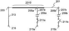
图3所示的电感器包括:具有矩形的螺线形状的布线(以下称为“螺线布线”)201;以及分别与螺线布线201的不同位置连接的多条引线213、207a、207b、207c。虽然图3所示的螺线布线201的整体的圈数为6,但该数只要是2以上即可。The inductor shown in FIG. 3 includes: a wiring having a rectangular spiral shape (hereinafter referred to as "spiral wiring") 201; and a plurality of
本实施方式中的螺线布线201由3个布线部分201a、201b、201c构成。图4为了明确地示出构成螺线布线201的布线部分201a、201b、201c和引线213、207a、207b、207c的关系,表示了假设将螺线布线201笔直延伸的状态的图。The
如图4中最清楚地所表示的,由螺线布线201的点203到点205a为止的范围由布线部分201a构成。再有,螺线布线201的点205a到点205b为止的范围由布线部分201b构成,点205b到点205c为止的范围由布线部分201c构成。其中,在螺线布线201上,连接引线的“点”并非一定是严格意义上的“点”,也可以是接触部具有有限面积的“面”。这些“点”表示各引线与螺线布线的连接部的“位置”。As shown most clearly in FIG. 4, the range from
在图中,比表示其他布线部分的线更粗地描绘了表示布线部分201a的线的一部分。在表示布线部分201a的线中相对粗的线的部分是在谐振频率f0下每单位长度的布线电阻比其他布线部分还低的低电阻部分2010。布线电阻依存于信号的频率。本发明中重要的“布线电阻”是谐振频率f0下的布线电阻的值。因此,在以下的说明中,“布线电阻”表示“谐振频率下的布线电阻”。In the drawing, a part of the line indicating the
为了使螺线布线上的特定部分中的每单位长度的布线电阻比其他部分更低,在该特定部分的布线材料中采用导电率高的材料或采用使布线数比其他部分有所增加的并联布线结构是非常有效的。在采用并联布线结构的情况下,更优选捻转并联配置的多条布线彼此来进行配置。图12是表示并联布线结构的一例的与长轴方向垂直的剖视图。图12(a)表示布线部分201b的剖面的一例,图12(b)表示布线部分201a中的低电阻部分2010的剖面的一例。在低电阻部分2010中,与布线部分201b等其他的布线部分相比,并联配置了更多根数的线材20。在低电阻部分2010中,如图12(c)所示,也可以不改变并联配置的线材20的根数,而是使线材20的直径比其他部分中的线材20的直径更大。In order to make the wiring resistance per unit length in a specific part of the spiral wiring lower than other parts, use a material with high conductivity in the wiring material of the specific part or use a parallel connection that increases the number of wirings compared to other parts. The wiring structure is very efficient. In the case of employing a parallel wiring structure, it is more preferable to twist and arrange a plurality of wirings arranged in parallel. 12 is a cross-sectional view perpendicular to the long-axis direction showing an example of a parallel wiring structure. FIG. 12(a) shows an example of a cross section of the
再有,图13表示布线部分201b的剖面的另一例。图13(a)表示布线部分201b的剖面的一例,图13(b)及图13(c)分别表示布线部分201a中的低电阻部分2010的剖面的例子。在图13(b)所示的低电阻部分2010中,没有改变并联配置的线材20的根数,而是使线材20的厚度比其他部分中的线材20的厚度更大。另外,在图13(c)所示的低电阻部分2010中,没有改变并联配置的线材20的根数,而是使线材20的宽度比其他部分中的线材20的宽度更大。在低电阻部分2010中,只要直径、厚度和/或宽度比其他部分中的值更大的线材的根数至少为1根即可。13 shows another example of the cross section of the
在螺线布线201中的布线部分201a的低电阻部分(粗实线部分)2010以外的部分中,每单位长度的电阻值既可以基本恒定,也可以是变化的。重要的是:在选择了电感值最低的状态时,与选择其他电感值的状态时相比,能实现以更低的阻抗高效率地工作的谐振器。In parts other than the low-resistance part (thick solid line part) 2010 of the
在本实施方式中,信号侧的引线213是1根,但接地侧的引线207a、207b、207c为多根。如后面的详细说明,通过从接地侧的引线207a、207b、207c中选择1根引线,从而能够切换电感值。在本实施方式中,虽然信号侧及接地侧的引线的总数为4根,但该总数只要为3根以上即可。In this embodiment, there is one
在图3的例子中,信号侧的引线、即第一引线213与成为螺线布线201的内侧终端的点203直接连接。另一方面,接地侧的引线组、即第二~第四引线207a、207b、207c分别与螺线布线的不同点205a、205b、205c连接。点203或点205c无需兼作螺线布线201的终端点。但是,因为没有必要使螺线布线201无谓地延伸,所以优选螺线布线201的两端与引线连接。In the example of FIG. 3 , the lead wire on the signal side, that is, the
第一引线213经由端子216与外部电路(图1的送电器103或图1的受电器109或者配置于送电器、受电器周边的匹配电路或滤波器电路等)连接,接受来自外部设备输出的能量供电或者向外部设备的能量供给。另一方面,第二引线207a与电容209a、导通路径选择开关211a及端子215a串联连接。第三引线207b与电容209b、导通路径选择开关211b及端子215b串联连接。第四引线207c与电容209c、导通路径选择开关211c及端子215c串联连接。The
引线207a、207b、207c中的一根经由从导通选择开关211a、211b、211c中选择并导通的一个开关,与端子215a、215b、215c中的一个连接。端子215a、215b、215c也与端子216成对地连接于外部电路的输入输出端子。One of the
电容209a、209b、209c的电容值被设定为:不依赖于选择性导通的开关,串联谐振电路的谐振频率表示恒定的值。在此,将分别选择了引线组207a、207b、207c时的电感值分别设为La、Lb、Lc。另外,将电容209a、209b、209c的电容值分别设为Ca、Cb、Cc。此时,预先调整Ca、Cb、Cc,以便即使从(La、Ca)、(Lb、Cb)、(Lc、Cc)这三组中选择任意一组,也可以以频率f0构成谐振电路。Capacitance values of the
根据上述构成,可以在将谐振频率保持f0不变的状态下从电感值与电容值的平衡不同的多个状态中选择一个状态。According to the above configuration, one state can be selected from a plurality of states in which the balance between the inductance value and the capacitance value is different while keeping the resonance frequency f0 constant.
谐振频率f0被设定为与进行无线电力传输的电磁能量的频率f0相同。更严谨的是,因为谐振器的制造偏差等主要原因,虽然能够在系统中利用以与传输频率不同的值进行谐振的谐振器,但不能有意地产生该差。通过在电感器与电容的平衡不同的多个状态间进行切换,从而在磁谐振方式的无线电力传输系统中实现具有可变阻抗特性的无线传输模块。The resonance frequency f0 is set to be the same as the frequency f0 of electromagnetic energy for wireless power transmission. More precisely, although a resonator resonating at a value different from the transmission frequency can be used in the system due to factors such as manufacturing variation of the resonator, the difference cannot be intentionally generated. A wireless transmission module having variable impedance characteristics is realized in a magnetic resonance system wireless power transmission system by switching between a plurality of states in which the balance between the inductor and the capacitor is different.
另外,例如在引线207a与端子215a之间电容209a及导通路径选择开关211a的配置顺序是任意的。也可以逆转电容209a及导通路径选择开关211a的配置顺序。即,也可以将电容209a连接到端子215a,将导通路径选择开关211a连接到引线207a。这对于其他引线、电容、开关、端子而言也是同样的。In addition, for example, the arrangement order of the
在本实施方式中,不是在布线部分201a的整条路径上配置了低电阻部分2010,而是仅在其一部分路径上配置了低电阻部分2010,但是本发明不限于这种例子。即,也可以由低电阻部分2010形成布线部分201a的整条路径。这样,若在布线部分201a的至少一部分路径上形成低电阻部分2010,则可以使布线电阻在整个布线部分201a上的平均值设得比整个其他布线部分201b、201c的平均值更小。In this embodiment, the low-
也可以在螺线布线201中的布线部分201a以外的部分、即布线部分201b、201c的一部分路径上与布线部分201a的低电阻部分2010同样地设置布线电阻低的部分。在这种情况下,也优选使布线电阻在整个布线部分201a上的平均值比整个其他布线部分201b、201c上的平均值更小。Similar to the low-
根据以上事实可知:本实施方式中的螺线布线201在从点203到点205a为止的范围(布线部分201a)内,具有将谐振频率下的每单位长度的布线电阻设置得比螺线布线201的其他范围的至少一部分还低的低电阻部分2010。其结果,螺线布线201的布线电阻在点203到点205a为止的整个范围内的平均值要比该范围外的平均值低。另外,最优选:设置在点203到点205a为止的范围内的低电阻部分2010在谐振频率下的每单位长度的布线电阻比其他任意部分在谐振频率下的每单位长度的布线电阻更低。From the above facts, it can be seen that the
通过采用上述构成,从而在本实施方式的可变谐振电路中,在选择了电感值最低的状态时,与选择了其他电感值的状态时相比,可以实现更低阻抗的谐振器。By adopting the above configuration, in the variable resonant circuit according to this embodiment, when the state with the lowest inductance value is selected, a resonator with lower impedance can be realized than when other inductance values are selected.
一般,在驱动恒压电路的情况下,在向负载提供更多电力时会流过更多的电流,成为低阻抗条件。另一方面,在以串联谐振电路进行磁谐振方式的无线电力传输的情况下,为了降低使传输效率最大化的输入输出端子中的最佳阻抗Zopt,优选实现谐振器的电感值小且电容值大的组合。Generally, when driving a constant-voltage circuit, more current flows when more power is supplied to the load, and this becomes a low-impedance condition. On the other hand, in the case of magnetic resonance wireless power transmission using a series resonant circuit, in order to reduce the optimum impedance Zopt in the input and output terminals for maximizing the transmission efficiency, it is preferable to achieve a resonator with a small inductance value and a small capacitance value. Great combination.
在图3的例子中,与使开关211b或开关211c导通的方式相比,使开关211a导通的方式会更缩短与谐振动作相关的螺线布线长度,因此串联谐振电路的电感值降低。在选择了电感值变为最小的状态时的螺线布线201的路径中包含布线电阻比其他部分更低的部分。结果,工作时可以成为阻抗更低且传输效率高的谐振器。In the example of FIG. 3 , turning on the
传输效率的阻抗依存性表示峰值时的最大传输效率由谐振器的Q值来决定。谐振器的Q值依存于构成谐振器的电感器的Q值和电容器的Q值。电感器的Q值具有随着电感器的圈数降低而降低的倾向。即,在越是低阻抗传输时越选择低电感值的状态的可变谐振器中,会导致谐振器的Q值降低、无线电力传输部的效率降低。为了改善电感器的Q值,降低电感器布线的每单位长度的电阻值是非常有效的。按照在布线的整条路径中实现低的电阻值的方式来设计电感器结构在实用上是不现实的。即,将全部布线置换为高导电率的布线的方法、或利用并联数高的并联布线结构来实现全部布线的方法会导致布线量增大引起的重量化、成本增大、占有容积的增大。The impedance dependence of transmission efficiency means that the maximum transmission efficiency at peak time is determined by the Q value of the resonator. The Q value of a resonator depends on the Q value of an inductor and the Q value of a capacitor constituting the resonator. The Q value of an inductor tends to decrease as the number of turns of the inductor decreases. That is, in a variable resonator in which a low inductance value is selected for transmission with lower impedance, the Q value of the resonator decreases and the efficiency of the wireless power transmission unit decreases. In order to improve the Q value of the inductor, it is very effective to reduce the resistance value per unit length of the inductor wiring. It is practically unrealistic to design the inductor structure so as to realize a low resistance value throughout the wiring path. That is, the method of replacing all the wiring with high-conductivity wiring, or the method of realizing all the wiring by using a parallel wiring structure with a high number of parallel connections, will result in increased weight, cost, and occupied volume due to the increase in the number of wiring. .
本实施方式中,选择低电感值时的谐振器中的布线路径是点203与点205a之间的路径。另一方面,选择高电感值时的谐振器中的布线路径是包含点205a到点205b为止的布线部分或者点205a到205c为止的布线部分的、更长的路径。虽然从点205a到点205b为止的布线部分在开关211b或开关211c导通时能够构成螺线布线的路径,但从点205b到点205c为止的布线部分仅在开关211c导通时才构成螺线布线的路径。In this embodiment, when a low inductance value is selected, the wiring path in the resonator is the path between the
在本实施方式中设定为:构成选择低电感值时的路径的布线部分的至少一部分路径在无线电力传输频率f0下的每单位长度的电阻值要比仅在选择高电感值时构成路径的布线部分(点205a与点205b之间的布线部分以及点205b与点205c之间的布线部分)在无线电力传输频率f0下的每单位长度的电阻值还要低。In this embodiment, it is set so that the resistance value per unit length at the wireless power transmission frequency f0 of at least a part of the wiring portion constituting the path when the low inductance value is selected is higher than that of the path that constitutes the path only when the high inductance value is selected. The wiring portion (the wiring portion between the
通过采用上述构成,从而可以以在低阻抗传输时选择的状态回避可变谐振器的Q值降低。在本实施方式中设计为越是电力传输量增多且要求高传输效率的条件就越能改善传输效率的劣化,且能回避布线量的增大。By adopting the above-mentioned configuration, it is possible to avoid a reduction in the Q value of the variable resonator in a state selected at the time of low-impedance transmission. In the present embodiment, it is designed that the deterioration of the transmission efficiency can be improved and the increase in the amount of wiring can be avoided as the power transmission amount increases and high transmission efficiency is required.
其中,流经开关211a、211b、211c的每一个开关的电流的大小互不相同。因此,优选根据假设成流经每个开关的电流的大小来适当地选择开关的尺寸或特性。例如,作为流过更大电流的开关,优选采用与流过更少电流的开关相比额定电流大的开关。再有,作为流过更大电流的开关,优选采用与流过更小电流的开关相比其栅极宽度相对较大的半导体元件。Wherein, the magnitude of the current flowing through each of the
(可变谐振器的动作停止控制)(Operation stop control of variable resonator)
在本发明的无线电力传输系统中想要停止充电供电动作的情况下,可通过将可变谐振器的谐振频率fr改变成与传输电磁能量的频率f0不同的值来应对。作为实现上述状态的方法,如图5所示,将导通路径选择开关全部选择为开放。再有,如图6所示,可以采用通过导通控制多个导通路径选择开关来使谐振频率不同于f0的方法等。In the wireless power transmission system of the present invention, when it is desired to stop the charging and feeding operation, it can be dealt with by changing the resonance frequency fr of the variable resonator to a value different from the frequency f0 of the electromagnetic energy transmitted. As a method of realizing the above state, as shown in FIG. 5 , all the conduction path selection switches are selected to be open. Furthermore, as shown in FIG. 6, a method of making the resonance frequency different from f0 by conducting conduction control of a plurality of conduction path selection switches, etc. may be employed.
图7是用于说明本发明的无线电力传输系统中的阻抗匹配的图。在图7中,省略了进行反馈控制的功能模块等。根据需要可以追加实现这些功能的未图示的模块。FIG. 7 is a diagram for explaining impedance matching in the wireless power transmission system of the present invention. In FIG. 7 , functional blocks performing feedback control and the like are omitted. Modules (not shown) that realize these functions can be added as needed.
匹配条件1:设计为使送电器103的输出阻抗ZTo与送电谐振器的最佳输入阻抗ZTx0一致。由此,能够降低送电器103与送电谐振器105之间的阻抗不匹配引起的能量反射。Matching condition 1: Design is such that the output impedance ZTo of the
匹配条件2:设计为使受电谐振器107的最佳输出阻抗ZRx0与受电器109的输入阻抗ZRi一致。由此,能够降低受电谐振器107与受电器109之间的阻抗不匹配引起的能量反射。Matching condition 2: Design is such that the optimum output impedance ZRx0 of the
匹配条件3:设计为使输入阻抗ZRi下的受电器109工作时的输出阻抗ZRo与负载阻抗RL一致。由此,能够降低受电器109与负载11之间的阻抗不匹配引起的能量反射。Matching condition 3: It is designed so that the output impedance ZRo of the
通过同时满足上述三个匹配条件,从而可以使传输效率最大化。另外,并非一定要同时满足上述三个匹配条件。By simultaneously satisfying the above three matching conditions, the transmission efficiency can be maximized. In addition, it is not necessary to satisfy the above three matching conditions at the same time.
(送电谐振器与受电谐振器的个数)(Number of power transmitting resonators and power receiving resonators)
传输系统内包含的送电谐振器与受电谐振器的台数并未分别限定于1。The number of power transmitting resonators and power receiving resonators included in the transmission system is not limited to one.
(电路元件的具体结构)(Specific structure of circuit components)
在送电谐振器与受电谐振器中,电容电路209a、209b、209c也可以利用芯片电容元件或陶瓷电容器、钽电解电容器、铝电解电容器、云母电容器、双电层电容器、真空电容器、在半导体工艺上形成的MIM结构等的集中常数电路元件来实现。再有,也可以考虑分布布线而产生的寄生电容的值来决定上述集中常数电路元件的电容值。In the power transmitting resonator and the power receiving resonator, the
构成送电谐振器105、受电谐振器107的电感器电路的螺线布线的形状并不限于矩形。既可以是椭圆形状,也可以是任意的非对称形状。在采用矩形螺线的形状的情况下,优选在角部具有一定以上的曲率。不包含角度急剧变化的部分的布线形状可以回避高频电流的集中、周边空间的磁场密度集中,可以提高传输效率。The shape of the spiral wiring constituting the inductor circuits of the
构成本发明的可变谐振器的螺线布线并不限于具有平面单层结构的布线。螺线布线也可以具有层叠结构。The spiral wiring constituting the variable resonator of the present invention is not limited to wiring having a planar single-layer structure. Spiral wiring may also have a stacked structure.
(实施方式2)(Embodiment 2)
接着,参照图8来说明本发明涉及的无线电力传输系统的第二实施方式。本实施方式与上述实施方式不同之处仅在于阻抗可变的串联谐振器的构成。因此,在此说明该串联谐振器的结构,对于其他结构不再重复相同的说明。Next, a second embodiment of the wireless power transmission system according to the present invention will be described with reference to FIG. 8 . This embodiment differs from the above-described embodiments only in the configuration of the series resonator with variable impedance. Therefore, the structure of the series resonator will be described here, and the same description will not be repeated for other structures.
在图3所示的实施方式中,将与外部端子216直接连接的信号侧的引线213连接到位于螺线布线201的螺线内侧的部分。相对于此,在本实施方式中,如图8所示,将信号侧的引线213连接到位于螺线布线201的螺线外侧的部分。In the embodiment shown in FIG. 3 , the
在本实施方式中,在选择开关211a时,成为电感值变为最低的状态。因此,在点203~点205a的布线部分201a的至少一部分中,与其他部分(点205a~点205b的布线部分201b或点205b~点205c的布线部分201c)相比,降低了传输频率f0下的每单位长度的电阻值。即使采用本实施方式的构成,也能实现与实施方式1中的串联谐振电路同样的效果。In the present embodiment, when the
然而,通过改善电感器的Q值,电流密度及磁场密度集中的螺线内部的布线电阻的降低能够取得相对更大的效果。因此,与图8的结构相比,更优选采用图3的构成。再有,在采用图3的结构的情况下,根据同样的理由,在实用问题上优选低电阻部分2010配置于螺线结构的最内周侧。However, by improving the Q value of the inductor, the reduction of the wiring resistance inside the spiral where the current density and the magnetic field density are concentrated can achieve a relatively greater effect. Therefore, it is more preferable to adopt the configuration of FIG. 3 than the configuration of FIG. 8 . Furthermore, when the structure of FIG. 3 is adopted, it is preferable to arrange the low-
(实施方式3)(Embodiment 3)
接着,参照图9对本发明涉及的无线电力传输系统的第三实施方式进行说明。本实施方式与上述实施方式的不同之处仅在于阻抗可变的串联谐振器的结构。因此,在此说明该串联谐振器的结构,对于其他结构不再重复相同的说明。Next, a third embodiment of the wireless power transmission system according to the present invention will be described with reference to FIG. 9 . The present embodiment differs from the above-described embodiments only in the structure of the impedance-variable series resonator. Therefore, the structure of the series resonator will be described here, and the same description will not be repeated for other structures.
在图3或图8所示的可变谐振器中,能选择电流路径的结构(开关电路)均仅针对接地侧的引线而存在。相对于此,在本实施方式中,如图9所示,对信号侧的引线也设置开关电路。具体是,选择性地连接2个信号输入侧端子216a、216b与2个引出点203a、203b。即,与引出点203a连接的引线213a经由开关212a与端子216a连接。另一方面,与引出点203b连接的引线213b经由开关212b与端子216b连接。选择性地导通多个开关212a、212b中的1个。In the variable resonator shown in FIG. 3 or FIG. 8 , the structure (switching circuit) capable of selecting the current path exists only for the lead wire on the ground side. On the other hand, in the present embodiment, as shown in FIG. 9 , a switch circuit is also provided on the lead wire on the signal side. Specifically, two signal
若将输入信号一侧的引线213a、213b、…的根数设为M,将接地侧的引线207a、207b、...的根数设为N,则最大能够得到M×N个电感值可变状态。If the number of
也可以在从引出点203a、203b到外部端子216a、216b为止的路径中插入电容元件。其中,此时,在谐振器工作中成为导通状态的开关的个数为2。另一方面,如图3的结构所示,在输入侧的引线213为1根的情况下,可以将工作中在谐振器内被选择控制为导通状态的导通路径选择开关的个数削减为1。即,在图3的结构中,与图9的结构相比,能够将谐振器中的开关导通损耗减半,由此提高传输效率。Capacitive elements may also be inserted in the paths from the
在上述各实施方式中,在阻抗变为最低的状态(假设了恒压动作时流过最大的电流的状态)下选择的路径包含着布线电阻比其他部分更低的部分。然而,本发明并不限于这种情况。例如,也可以在使用频度最高的布线部分或使用时间最长的布线部分的至少一部分路径中设置布线电阻比其他部分的至少一部分还低的部分(低电阻部分2010)。In each of the above-described embodiments, the path selected in the state where the impedance is the lowest (assuming a state where the largest current flows during constant voltage operation) includes a portion whose wiring resistance is lower than other portions. However, the present invention is not limited to this case. For example, a portion (low resistance portion 2010 ) having a wiring resistance lower than at least a part of other portions may be provided in at least a part of the route of the most frequently used wiring portion or the longest used wiring portion.
另外,图10及图11分别是表示针对其他实施方式而言假设将螺线布线201笔直延伸的状态的图。图10所示的螺线布线201也在从点203b到点205a为止的范围内具有低电阻部分2010,该低电阻部分2010设定为谐振频率下的每单位长度的布线电阻要比螺线布线201的其他范围内的至少一部分更低。其中,在该例子中,也可以在点203a到点203b为止的范围的一部分设置低电阻部分2010。In addition, FIGS. 10 and 11 are diagrams each showing a state in which the
图11所示的螺线布线201也在从点203到点205a为止的范围内具有低电阻部分2010,该低电阻部分设定为谐振频率下的每单位长度的布线电阻要比螺线布线201的其他范围内的至少一部分更低。其中,在该例子中,也可以在点205a到点205b为止的范围的一部分设置低电阻部分2010。The
(实施例)(Example)
为了实际验证本发明的有利效果,制作了具有图3所示的结构的可变谐振器。具体是,制作了以下的表1所示的实施例及比较例。制作的顺序如下所述。In order to actually verify the advantageous effects of the present invention, a variable resonator having the structure shown in FIG. 3 was fabricated. Specifically, Examples and Comparative Examples shown in Table 1 below were prepared. The sequence of making is described below.
首先,以长方形状中长边a=30cm、短边b=16cm、相邻布线间隔1cm、最大圈数为6的条件制作了螺线布线(电感器布线)。为了降低谐振器的导体损耗,由并列排列多根直径120微米的铜布线而成的绞合线(Litzwire)形成螺线布线。螺线布线的每单位长度的布线电阻随着构成绞合线的并列铜布线的根数而变化。在实施例1中,由并列根数为60根的布线部分、150根布线部分、250根的布线部分构成螺线布线。在比较例1a中,由并列根数为60根的布线构成螺线布线整体。在比较例1b中,由并列根数为250根的布线构成螺线布线整体。First, spiral wiring (inductor wiring) was produced under the conditions of long side a = 30 cm, short side b = 16 cm, interval between adjacent wirings 1 cm, and maximum number of turns 6 in a rectangular shape. In order to reduce the conductor loss of the resonator, a twisted wire (Litzwire) formed by arranging a plurality of copper wires with a diameter of 120 microns in parallel forms a spiral wire. The wiring resistance per unit length of the spiral wiring varies with the number of parallel copper wirings constituting the twisted wire. In Example 1, the spiral wiring is composed of 60 wiring sections, 150 wiring sections, and 250 wiring sections. In Comparative Example 1a, the entire spiral wiring is composed of 60 parallel wirings. In Comparative Example 1b, the entire spiral wiring is composed of 250 parallel wirings.
无论在哪个可变谐振器中,都将螺线最内部的终端点设为点203,并经由引线213而连接到外部电路的信号线。再有,在从螺线最内部的一端开始数起,在圈数为2的位置设置分支点205a,在圈数为4的位置设置分支点205b,将最外部的终端点(圈数为6的位置)设为点205c。在点205a、205b、205c上分别连接引线207a、207b、207c。引线207a、207b、207c分别经由电容209a、209b、209c而连接到负载开关211a、211b、211c。In any variable resonator, the innermost terminal point of the spiral is set at
在实施例1中,螺线布线的从终端点203到分支点205a为止的部分由并列根数为250根的布线部分构成,该部分的布线电阻最低。螺线布线的从分支点205a到分支点205b为止的部分由并列根数为150根的布线部分构成。螺线布线的从分支点205b到终端点205c为止的部分由并列根数为60根的布线部分构成,该部分的布线电阻最高。In Example 1, the part of the spiral wiring from the
另一方面,在比较例1a中,螺线布线的从一个终端点203到另一个终端点205a为止的整体都由并列根数为60根的布线构成。在比较例1b中,螺线布线的从一个终端点203到另一个终端点205a为止的整体都由并列根数为250根的布线构成。On the other hand, in Comparative Example 1a, the spiral wiring from one
负载开关211a、211b、211c均为具有30mΩ的导通(ON)电阻的MOSFET。负载开关211a、211b、211c连接到外部电路的输入输出端子的GND。通过使负载开关211a、211b、211c中的1个导通,从而选择螺线布线201的从点203到点215a、215b、215c的任一个点为止的路径,可以使电感值可变。Each of the
在负载开关211a、211b、211c的任意一个被选择性导通的情况下,即使选择哪一个负载开关,都能按照串联谐振电路的谐振频率为1.8MHz的方式设定电容209a、209b、209c的电容值。具体是,将电容209a、209b、209c的电容值分别设定为3640pF(皮法)、1070pF、500pF。When any one of the
在进行低阻抗传输时选择开关211a,使用圈数为2的电感器有助于谐振。再有,在进行高阻抗传输时选择开关211c,使用圈数为6的电感器有助于谐振。在进行中阻抗传输时选择开关211b,使用圈数为4的电感器有助于谐振。
对于实施例1、比较例1a、比较例1b的每一个而言,各制作2个绞合线的并列布线根数如表1所示那样不同的谐振器,作为谐振器的低损耗性的指标,测量了Q值。For each of Example 1, Comparative Example 1a, and Comparative Example 1b, two resonators having different numbers of twisted wires wired in parallel as shown in Table 1 were produced, and used as an index of low-loss properties of the resonators. , the Q value was measured.
再有,将同一条件的谐振器作为送电及受电谐振器的对,将电感器的形成面平行地离开20cm进行配置。将两天线的输入输出端子连接到网络分析仪,以小信号输入条件测量了通过/反射特性。这样,测量了将天线间传输效率最大化的最佳阻抗值及最大传输效率。接着,向送电侧的天线提供50W的能量,在利用受电天线进行受电的情况下,测量了送电及受电天线(送受電アンテナ)中产生的热量。In addition, resonators under the same conditions were used as a pair of power transmission and power reception resonators, and the formation planes of the inductors were arranged parallel to each other at a distance of 20 cm. The input and output terminals of the two antennas were connected to a network analyzer, and the pass/reflection characteristics were measured under a small-signal input condition. In this way, the optimum impedance value for maximizing the transmission efficiency between the antennas and the maximum transmission efficiency were measured. Next, 50 W of energy was supplied to the antenna on the power transmitting side, and when power was received by the power receiving antenna, the heat generated in the power transmitting and receiving antenna (power transmitting and receiving antenna) was measured.
表1中示出实施例1及比较例1a、1b的结构、传输特性、以50W传输时产生的热量。再有,也在表1中示出将用于比较例1a中的布线量设为100时的实施例与比较例的总布线量。Table 1 shows the structure, transmission characteristics, and heat generated at the time of transmission at 50W of Example 1 and Comparative Examples 1a and 1b. In addition, Table 1 also shows the total wiring quantity of the Example and the comparative example when the wiring quantity used in the comparative example 1a was set to 100.
[表1][Table 1]


如表1所示,比较例1a的低阻抗传输时(选择开关211a且使用圈数为2)的发生损耗与高阻抗传输时(选择开关211c且使用圈数为6)相比达到63倍,在实用方面进行改善是有必要的。As shown in Table 1, the loss during low-impedance transmission (
另一方面,在实施例1中,尤其是在低阻抗传输时,与比较例1a相比传输效率得到了大幅度的改善。低阻抗传输时的发生损耗与比较例1a相比降低87%,在实用方面得到了非常有用的效果(高阻抗传输时降低59%)。On the other hand, in Example 1, especially in low-impedance transmission, the transmission efficiency was greatly improved compared with Comparative Example 1a. The generation loss during low-impedance transmission was reduced by 87% compared with Comparative Example 1a, and a very useful effect was obtained practically (59% reduction during high-impedance transmission).
在比较例1b中,达成三例中最高的传输效率。然而,与比较例1a相比,必须使用3.3倍的布线。而且,比较例1b与实施例1相比,尽管布线量也增加了64%,但低阻抗传输时的发生损耗只能够削减25%。还有,可知:虽然高阻抗传输时的发生损耗削减了40%,但比较例1b的效率与实施例1或比较例1a的效率之差极小。In Comparative Example 1b, the highest transfer efficiency among the three examples was achieved. However, compared with Comparative Example 1a, 3.3 times the wiring had to be used. Furthermore, in Comparative Example 1b, compared with Example 1, although the amount of wiring was increased by 64%, the loss generated during low-impedance transmission could only be reduced by 25%. In addition, it can be seen that the difference between the efficiency of Comparative Example 1b and the efficiency of Example 1 or Comparative Example 1a is extremely small, although the loss occurring during high-impedance transmission is reduced by 40%.
如上所述,实际验证了能以较少的布线使用量有效地改善大电力传输时的效率这样的本发明特有的效果。As described above, it has actually been verified that the unique effect of the present invention is that the efficiency at the time of large power transmission can be effectively improved with a small amount of wiring used.
另外,在实施例1中,虽然将固定引线设置在螺线的内侧终端点,但制作了将固定引线设定到螺线的外侧终端点侧的实施例2。在实施例2中,与实施例1相反,从螺线布线外侧开始按照每2圈将绞合线的并列根数设为100、60、30。在实施例2中,在使用圈数2中得到了861的Q值,在使用圈数6中得到了1811的Q值。实施例2与比较例1a相比为2.19倍的布线使用量。实施例2虽然在布线使用效率及Q值的特性上都比实施例1差一些,但是还是验证了本发明的有用效果。In addition, in Example 1, although the fixed lead was provided at the inner end point of the spiral, Example 2 was produced in which the fixed lead was set at the outer end point of the spiral. In Example 2, contrary to Example 1, the number of parallel twisted wires was set to 100, 60, and 30 every two turns from the outside of the spiral wiring. In Example 2, a Q value of 861 was obtained when the number of turns 2 was used, and a Q value of 1811 was obtained when the number of turns 6 was used. In Example 2, the wiring usage was 2.19 times that of Comparative Example 1a. Although Embodiment 2 is inferior to Embodiment 1 in terms of wiring efficiency and Q value characteristics, it still demonstrates the useful effect of the present invention.
其中,本发明的无线电力传输系统的利用范围并非一定要限于恒压驱动系统。Wherein, the scope of application of the wireless power transmission system of the present invention is not necessarily limited to the constant voltage drive system.
(工业上的可利用性)(industrial availability)
本发明涉及的无线电力传输系统可以应用于个人计算机、笔记本型个人计算机等办公设备或壁挂式电视机、移动AV设备等AV设备。该无线电力传输系统不仅可以应用于对助听器、医疗保健(health care)设备的充电供电中,还可以应用于电动汽车、电动自行车、移动机器人的行驶中充电系统、停车中充电系统等。进而,也可以应用于与来自太阳电池或燃料电池的集电系统、直流供电系统中的设备的连接场所、交流插座替代品等比较广泛的领域。The wireless power transmission system of the present invention can be applied to office equipment such as personal computers and notebook personal computers, or AV equipment such as wall-mounted TV sets and mobile AV equipment. The wireless power transmission system can not only be applied to charging and supplying hearing aids and healthcare (health care) equipment, but also can be applied to driving charging systems of electric vehicles, electric bicycles, mobile robots, parking charging systems, etc. Furthermore, it can also be applied to a relatively wide range of fields such as a power collection system from a solar cell or a fuel cell, a connection place of equipment in a DC power supply system, and a substitute for an AC outlet.
符号说明Symbol Description
20构成螺线布线的线材20 wires that make up the helical wiring
101 电源101 power supply
103 送电器103 Transmitter
105 送电谐振器105 power transmission resonator
105a 电感器105a inductor
105b 电容元件105b capacitive element
107 受电谐振器107 powered resonator
107a 电感器107a Inductor
107b 电容元件107b capacitive element
109 受电器109 Receiver
111 负载111 load
201 螺线布线201 spiral wiring
201a、201b、201c 布线部分201a, 201b, 201c wiring part
203 螺线布线的终端点203 Terminal point of spiral wiring
205a、205b、205c、203a、203b 螺线布线上的任意点205a, 205b, 205c, 203a, 203b Any point on the spiral wiring
207a、207b、207c 接地侧的引线组207a, 207b, 207c Lead wire set on ground side
209a、209b、209c 电容209a, 209b, 209c capacitor
211a、211b、211c 导通路径选择开关211a, 211b, 211c conduction path selection switch
212a、212b 导通路径选择开关212a, 212b conduction path selection switch
213、213a、213b 信号输入侧的引线213, 213a, 213b Lead wires on the signal input side
215a、215b、215c 端子215a, 215b, 215c terminals
216、216a、216b 端子216, 216a, 216b terminals
220 引线选择部220 Lead Selection Section
2010 螺线布线的低电阻部分2010 Low Resistance Section of Spiral Wiring
Claims (20)
Applications Claiming Priority (3)
| Application Number | Priority Date | Filing Date | Title |
|---|---|---|---|
| US31880710P | 2010-03-30 | 2010-03-30 | |
| US61/318,807 | 2010-03-30 | ||
| PCT/JP2011/001867WO2011122003A1 (en) | 2010-03-30 | 2011-03-29 | Wireless power transmission system |
Publications (2)
| Publication Number | Publication Date |
|---|---|
| CN102414957Atrue CN102414957A (en) | 2012-04-11 |
| CN102414957B CN102414957B (en) | 2014-12-10 |
Family
ID=44708774
Family Applications (1)
| Application Number | Title | Priority Date | Filing Date |
|---|---|---|---|
| CN201180001906.XAActiveCN102414957B (en) | 2010-03-30 | 2011-03-29 | Wireless power transmission system |
Country Status (5)
| Country | Link |
|---|---|
| US (1) | US8716900B2 (en) |
| EP (1) | EP2555376B1 (en) |
| JP (1) | JP5810291B2 (en) |
| CN (1) | CN102414957B (en) |
| WO (1) | WO2011122003A1 (en) |
Cited By (13)
| Publication number | Priority date | Publication date | Assignee | Title |
|---|---|---|---|---|
| CN103346626A (en)* | 2013-07-31 | 2013-10-09 | 哈尔滨工业大学 | Multi-load wireless energy transmission device with auxiliary terminal inductance frequency selection |
| CN103346627A (en)* | 2013-07-31 | 2013-10-09 | 哈尔滨工业大学 | Multi-load wireless energy transmission device with primary end inductance frequency selection |
| CN103779973A (en)* | 2010-04-07 | 2014-05-07 | 松下电器产业株式会社 | Wireless power transmission system, and inductor used in wireless power transmission system |
| TWI558056B (en)* | 2015-12-04 | 2016-11-11 | 財團法人工業技術研究院 | Solar battery structure with wireless charging |
| CN106663967A (en)* | 2014-09-10 | 2017-05-10 | 罗伯特·博世有限公司 | Transmission coil for inductive energy transfer |
| CN108401472A (en)* | 2015-12-22 | 2018-08-14 | 英特尔公司 | Uniform wireless charging device |
| CN108429356A (en)* | 2017-02-15 | 2018-08-21 | 三星电机株式会社 | wireless power transmitter |
| CN110073572A (en)* | 2016-09-16 | 2019-07-30 | Tdk电子股份有限公司 | Wireless power transmitter, Wireless power transmission system and the method for driving Wireless power transmission system |
| CN110112835A (en)* | 2019-05-16 | 2019-08-09 | 中南大学 | Four loop construction magnet coupled resonant type wireless energy transmission system of frequency reconfigurable |
| CN110800211A (en)* | 2017-06-28 | 2020-02-14 | 株式会社村田制作所 | High-frequency filter, multiplexer, high-frequency front-end circuit, and communication device |
| CN111681847A (en)* | 2015-08-07 | 2020-09-18 | 纽卡润特有限公司 | Device with a multi-mode antenna with variable conductor width |
| US11469598B2 (en) | 2015-08-07 | 2022-10-11 | Nucurrent, Inc. | Device having a multimode antenna with variable width of conductive wire |
| US11955809B2 (en) | 2015-08-07 | 2024-04-09 | Nucurrent, Inc. | Single structure multi mode antenna for wireless power transmission incorporating a selection circuit |
Families Citing this family (72)
| Publication number | Priority date | Publication date | Assignee | Title |
|---|---|---|---|---|
| US8855554B2 (en) | 2008-03-05 | 2014-10-07 | Qualcomm Incorporated | Packaging and details of a wireless power device |
| EP2277252A4 (en) | 2008-04-21 | 2017-04-26 | Qualcomm Incorporated | Short range efficient wireless power transfer |
| US8497658B2 (en)* | 2009-01-22 | 2013-07-30 | Qualcomm Incorporated | Adaptive power control for wireless charging of devices |
| US11476566B2 (en) | 2009-03-09 | 2022-10-18 | Nucurrent, Inc. | Multi-layer-multi-turn structure for high efficiency wireless communication |
| US9479225B2 (en) | 2010-05-13 | 2016-10-25 | Qualcomm Incorporated | Resonance detection and control within a wireless power system |
| JP2011259534A (en)* | 2010-06-05 | 2011-12-22 | Sanyo Electric Co Ltd | Battery-integrated apparatus and charging stand |
| JP5674013B2 (en)* | 2010-10-08 | 2015-02-18 | ソニー株式会社 | Power supply device and power supply system |
| US9094055B2 (en) | 2011-04-19 | 2015-07-28 | Qualcomm Incorporated | Wireless power transmitter tuning |
| US9071284B2 (en) | 2011-10-21 | 2015-06-30 | Qualcomm Incorporated | Load impedance detection for static or dynamic adjustment of passive loads |
| KR101851590B1 (en)* | 2011-11-28 | 2018-04-25 | 삼성전자주식회사 | Wireless power transmission system and multi mode resonator in wireless power transmission system |
| US9196419B2 (en)* | 2011-11-29 | 2015-11-24 | Panasonic Intellectual Property Management Co., Ltd. | Wireless electric power transmission apparatus |
| JP6029278B2 (en) | 2011-12-21 | 2016-11-24 | ソニー株式会社 | Power receiving device and non-contact power transmission system |
| US10352970B2 (en) | 2011-12-21 | 2019-07-16 | Sony Corporation | Detection apparatus, power receiving apparatus, non-contact power transmission system and detection method |
| US9431856B2 (en) | 2012-01-09 | 2016-08-30 | Pabellon, Inc. | Power transmission |
| KR101697418B1 (en)* | 2012-05-09 | 2017-01-17 | 도요타지도샤가부시키가이샤 | Vehicle |
| KR101601352B1 (en)* | 2012-09-26 | 2016-03-08 | 엘지이노텍 주식회사 | Apparatus for transmitting wireless power and method for controlling power thereof |
| KR101984811B1 (en) | 2012-10-23 | 2019-06-03 | 삼성전자주식회사 | Field controllable 3d flexible resonator for wireless power transfer system |
| KR102166686B1 (en)* | 2012-10-26 | 2020-10-16 | 엘지전자 주식회사 | Wireless power transmitting apparatus |
| JP6282398B2 (en)* | 2013-02-19 | 2018-02-21 | 矢崎総業株式会社 | Electromagnetic induction coil |
| KR102042685B1 (en) | 2013-03-14 | 2019-11-11 | 삼성전자주식회사 | Wireless power transmission apparatus and wireless power reception apparatus |
| KR102125917B1 (en) | 2013-08-07 | 2020-07-08 | 엘지이노텍 주식회사 | Wireless power transmitting device |
| KR102109764B1 (en)* | 2013-09-13 | 2020-05-29 | 삼성전자주식회사 | Method of determining location of power receiving unit in power transmitting unit and the power transmitting unit |
| JP6258816B2 (en) | 2013-10-29 | 2018-01-10 | パナソニック株式会社 | Wireless power transmission apparatus and wireless power transmission system |
| TWI513135B (en)* | 2013-11-18 | 2015-12-11 | Richtek Technology Corp | Power management unit and wireless power system thereof |
| US10164472B2 (en) | 2013-12-03 | 2018-12-25 | Massachusetts Institute Of Technology | Method and apparatus for wirelessly charging portable electronic devices |
| WO2015097813A1 (en)* | 2013-12-26 | 2015-07-02 | 三菱電機エンジニアリング株式会社 | Resonant power-transfer device |
| US9379555B2 (en)* | 2014-04-30 | 2016-06-28 | Active-Semi, Inc. | Adaptive power source for wireless power transmitter |
| KR102134430B1 (en) | 2014-05-21 | 2020-07-15 | 삼성전자주식회사 | Wireless power receiving device and method to receive power wirelessly based on switching |
| WO2016072707A1 (en)* | 2014-11-03 | 2016-05-12 | 주식회사 한림포스텍 | Wireless power transmission and charging system |
| WO2016099032A1 (en) | 2014-12-16 | 2016-06-23 | 주식회사 한림포스텍 | Apparatus and method for controlling power transmission coverage of wireless power transmission network |
| KR20160051497A (en) | 2014-11-03 | 2016-05-11 | 주식회사 한림포스텍 | Method and apparutus for controlling a power transmission coverage of wireless power transmission network |
| GB2533695B (en)* | 2014-12-23 | 2018-02-21 | Intel Corp | Coil topology for wireless charging |
| US10498160B2 (en) | 2015-08-03 | 2019-12-03 | Massachusetts Institute Of Technology | Efficiency maximization for device-to-device wireless charging |
| US10636563B2 (en) | 2015-08-07 | 2020-04-28 | Nucurrent, Inc. | Method of fabricating a single structure multi mode antenna for wireless power transmission using magnetic field coupling |
| US11205848B2 (en) | 2015-08-07 | 2021-12-21 | Nucurrent, Inc. | Method of providing a single structure multi mode antenna having a unitary body construction for wireless power transmission using magnetic field coupling |
| US9941590B2 (en)* | 2015-08-07 | 2018-04-10 | Nucurrent, Inc. | Single structure multi mode antenna for wireless power transmission using magnetic field coupling having magnetic shielding |
| US9948129B2 (en)* | 2015-08-07 | 2018-04-17 | Nucurrent, Inc. | Single structure multi mode antenna for wireless power transmission using magnetic field coupling having an internal switch circuit |
| US9941743B2 (en)* | 2015-08-07 | 2018-04-10 | Nucurrent, Inc. | Single structure multi mode antenna having a unitary body construction for wireless power transmission using magnetic field coupling |
| US9941729B2 (en)* | 2015-08-07 | 2018-04-10 | Nucurrent, Inc. | Single layer multi mode antenna for wireless power transmission using magnetic field coupling |
| US9960629B2 (en)* | 2015-08-07 | 2018-05-01 | Nucurrent, Inc. | Method of operating a single structure multi mode antenna for wireless power transmission using magnetic field coupling |
| US9960628B2 (en) | 2015-08-07 | 2018-05-01 | Nucurrent, Inc. | Single structure multi mode antenna having a single layer structure with coils on opposing sides for wireless power transmission using magnetic field coupling |
| US10985465B2 (en)* | 2015-08-19 | 2021-04-20 | Nucurrent, Inc. | Multi-mode wireless antenna configurations |
| US20170085115A1 (en)* | 2015-09-23 | 2017-03-23 | Intel Corporation | Method, system and apparatus for alternative power wireless charging |
| US20170085130A1 (en)* | 2015-09-23 | 2017-03-23 | Qualcomm Incorporated | Multifilament transmitter coupler with current sharing |
| GB2543343A (en)* | 2015-10-16 | 2017-04-19 | Bombardier Transp Gmbh | Receiving device for receiving an electromagnetic field and for producing an alternating electric current by magnetic induction, method of operating the recei |
| JP6868841B2 (en)* | 2016-02-19 | 2021-05-12 | パナソニックIpマネジメント株式会社 | Electric device |
| US20180062434A1 (en) | 2016-08-26 | 2018-03-01 | Nucurrent, Inc. | Wireless Connector Receiver Module Circuit |
| US10432031B2 (en) | 2016-12-09 | 2019-10-01 | Nucurrent, Inc. | Antenna having a substrate configured to facilitate through-metal energy transfer via near field magnetic coupling |
| US11502547B2 (en) | 2017-02-13 | 2022-11-15 | Nucurrent, Inc. | Wireless electrical energy transmission system with transmitting antenna having magnetic field shielding panes |
| KR102268987B1 (en) | 2017-04-07 | 2021-06-24 | 광동 오포 모바일 텔레커뮤니케이션즈 코포레이션 리미티드 | Wireless charging device, wireless charging method and charging standby equipment |
| US11283295B2 (en) | 2017-05-26 | 2022-03-22 | Nucurrent, Inc. | Device orientation independent wireless transmission system |
| GB201721863D0 (en)* | 2017-12-24 | 2018-02-07 | Vivoplex Group Ltd | Monitoring system |
| US10651687B2 (en) | 2018-02-08 | 2020-05-12 | Massachusetts Institute Of Technology | Detuning for a resonant wireless power transfer system including cryptography |
| US11018526B2 (en) | 2018-02-08 | 2021-05-25 | Massachusetts Institute Of Technology | Detuning for a resonant wireless power transfer system including cooperative power sharing |
| DE102018118572A1 (en)* | 2018-07-31 | 2020-02-06 | Zollner Elektronik Ag | Inductive charging arrangement with split wire |
| US12249847B2 (en) | 2018-12-31 | 2025-03-11 | 3M Innovative Properties Company | Wireless power transfer |
| KR20210001160A (en)* | 2019-06-27 | 2021-01-06 | 세메스 주식회사 | Wireless power transfering apparatus |
| US11271430B2 (en) | 2019-07-19 | 2022-03-08 | Nucurrent, Inc. | Wireless power transfer system with extended wireless charging range |
| US11227712B2 (en) | 2019-07-19 | 2022-01-18 | Nucurrent, Inc. | Preemptive thermal mitigation for wireless power systems |
| KR102261860B1 (en)* | 2019-09-09 | 2021-06-07 | 엘지전자 주식회사 | Multi-level power compatible wireless power receiving apparatus |
| US11056922B1 (en) | 2020-01-03 | 2021-07-06 | Nucurrent, Inc. | Wireless power transfer system for simultaneous transfer to multiple devices |
| WO2022005526A1 (en)* | 2020-06-30 | 2022-01-06 | Google Llc | Multi-gauge stranded coil for wireless charging |
| US11283303B2 (en) | 2020-07-24 | 2022-03-22 | Nucurrent, Inc. | Area-apportioned wireless power antenna for maximized charging volume |
| US11876386B2 (en) | 2020-12-22 | 2024-01-16 | Nucurrent, Inc. | Detection of foreign objects in large charging volume applications |
| US11881716B2 (en) | 2020-12-22 | 2024-01-23 | Nucurrent, Inc. | Ruggedized communication for wireless power systems in multi-device environments |
| US11695302B2 (en) | 2021-02-01 | 2023-07-04 | Nucurrent, Inc. | Segmented shielding for wide area wireless power transmitter |
| EP4313668A1 (en)* | 2021-04-01 | 2024-02-07 | Veturex Inc. | A plug-in module for wireless charging |
| KR20220169152A (en) | 2021-06-18 | 2022-12-27 | 삼성전자주식회사 | Semiconductor device |
| JP7550806B2 (en) | 2022-02-10 | 2024-09-13 | 大井電気株式会社 | Coil for non-contact power supply and variable diameter coil for non-contact power supply |
| US11831174B2 (en) | 2022-03-01 | 2023-11-28 | Nucurrent, Inc. | Cross talk and interference mitigation in dual wireless power transmitter |
| US12003116B2 (en) | 2022-03-01 | 2024-06-04 | Nucurrent, Inc. | Wireless power transfer system for simultaneous transfer to multiple devices with cross talk and interference mitigation |
| TWI819902B (en)* | 2022-11-21 | 2023-10-21 | 國立成功大學 | Wireless power transfer device and system |
Citations (4)
| Publication number | Priority date | Publication date | Assignee | Title |
|---|---|---|---|---|
| CN101438480A (en)* | 2007-07-13 | 2009-05-20 | 翰林Postech株式会社 | Non-contact charger system for wireless power transmission of battery and control method thereof |
| CN101447684A (en)* | 2007-11-30 | 2009-06-03 | 郑春吉 | Wireless power charging system |
| JP2009125097A (en)* | 2007-11-19 | 2009-06-11 | Olympus Corp | Radio feed system |
| JP2009268181A (en)* | 2008-04-22 | 2009-11-12 | Olympus Corp | Energy supply apparatus |
Family Cites Families (9)
| Publication number | Priority date | Publication date | Assignee | Title |
|---|---|---|---|---|
| JPH08175232A (en) | 1994-12-22 | 1996-07-09 | Toyota Autom Loom Works Ltd | Noncontact power feeding system |
| US6649842B1 (en) | 1999-02-10 | 2003-11-18 | Daifuku Co., Ltd. | Power feeding facility and its cable for high-frequency current |
| US7212414B2 (en) | 1999-06-21 | 2007-05-01 | Access Business Group International, Llc | Adaptive inductive power supply |
| JP2001344574A (en) | 2000-05-30 | 2001-12-14 | Mitsubishi Materials Corp | Antenna device for interrogator |
| US7825543B2 (en) | 2005-07-12 | 2010-11-02 | Massachusetts Institute Of Technology | Wireless energy transfer |
| EP1788626B1 (en) | 2005-11-17 | 2009-04-29 | Seiko Epson Corporation | Multilayer circuit with variable inductor, and method of manufacturing it |
| JP4930093B2 (en) | 2007-02-21 | 2012-05-09 | セイコーエプソン株式会社 | Power transmission control device, power reception control device, non-contact power transmission system, power transmission device, power reception device, and electronic equipment |
| US8610312B2 (en)* | 2007-09-17 | 2013-12-17 | Hideo Kikuchi | Induced power transmission circuit |
| WO2010036279A1 (en)* | 2007-11-28 | 2010-04-01 | Qualcomm Incorporated | Wireless power range increase using parasitic antennas |
- 2011
- 2011-03-29WOPCT/JP2011/001867patent/WO2011122003A1/enactiveApplication Filing
- 2011-03-29USUS13/075,096patent/US8716900B2/enactiveActive
- 2011-03-29JPJP2011536219Apatent/JP5810291B2/enactiveActive
- 2011-03-29CNCN201180001906.XApatent/CN102414957B/enactiveActive
- 2011-03-29EPEP11762250.6Apatent/EP2555376B1/enactiveActive
Patent Citations (4)
| Publication number | Priority date | Publication date | Assignee | Title |
|---|---|---|---|---|
| CN101438480A (en)* | 2007-07-13 | 2009-05-20 | 翰林Postech株式会社 | Non-contact charger system for wireless power transmission of battery and control method thereof |
| JP2009125097A (en)* | 2007-11-19 | 2009-06-11 | Olympus Corp | Radio feed system |
| CN101447684A (en)* | 2007-11-30 | 2009-06-03 | 郑春吉 | Wireless power charging system |
| JP2009268181A (en)* | 2008-04-22 | 2009-11-12 | Olympus Corp | Energy supply apparatus |
Cited By (22)
| Publication number | Priority date | Publication date | Assignee | Title |
|---|---|---|---|---|
| CN103779973A (en)* | 2010-04-07 | 2014-05-07 | 松下电器产业株式会社 | Wireless power transmission system, and inductor used in wireless power transmission system |
| CN103779973B (en)* | 2010-04-07 | 2016-03-16 | 松下知识产权经营株式会社 | Wireless power transmission system and for the inductor in this Wireless power transmission system |
| CN103346627A (en)* | 2013-07-31 | 2013-10-09 | 哈尔滨工业大学 | Multi-load wireless energy transmission device with primary end inductance frequency selection |
| CN103346627B (en)* | 2013-07-31 | 2015-09-16 | 哈尔滨工业大学 | The multi-load wireless energy transform device of former end inductance frequency-selecting |
| CN103346626A (en)* | 2013-07-31 | 2013-10-09 | 哈尔滨工业大学 | Multi-load wireless energy transmission device with auxiliary terminal inductance frequency selection |
| CN106663967A (en)* | 2014-09-10 | 2017-05-10 | 罗伯特·博世有限公司 | Transmission coil for inductive energy transfer |
| CN111681847A (en)* | 2015-08-07 | 2020-09-18 | 纽卡润特有限公司 | Device with a multi-mode antenna with variable conductor width |
| US12136514B2 (en) | 2015-08-07 | 2024-11-05 | Nucurrent, Inc. | Device having a multimode antenna with variable width of conductive wire |
| US11955809B2 (en) | 2015-08-07 | 2024-04-09 | Nucurrent, Inc. | Single structure multi mode antenna for wireless power transmission incorporating a selection circuit |
| US11769629B2 (en) | 2015-08-07 | 2023-09-26 | Nucurrent, Inc. | Device having a multimode antenna with variable width of conductive wire |
| US11469598B2 (en) | 2015-08-07 | 2022-10-11 | Nucurrent, Inc. | Device having a multimode antenna with variable width of conductive wire |
| TWI558056B (en)* | 2015-12-04 | 2016-11-11 | 財團法人工業技術研究院 | Solar battery structure with wireless charging |
| CN106847979B (en)* | 2015-12-04 | 2019-06-07 | 财团法人工业技术研究院 | Solar cell structure with wireless charging function |
| US10249778B2 (en) | 2015-12-04 | 2019-04-02 | Industrial Technology Research Institute | Solar cell structure for wireless charging |
| CN106847979A (en)* | 2015-12-04 | 2017-06-13 | 财团法人工业技术研究院 | Solar cell structure with wireless charging function |
| CN108401472B (en)* | 2015-12-22 | 2022-06-17 | 英特尔公司 | Uniform wireless charging device |
| CN108401472A (en)* | 2015-12-22 | 2018-08-14 | 英特尔公司 | Uniform wireless charging device |
| CN110073572A (en)* | 2016-09-16 | 2019-07-30 | Tdk电子股份有限公司 | Wireless power transmitter, Wireless power transmission system and the method for driving Wireless power transmission system |
| CN108429356A (en)* | 2017-02-15 | 2018-08-21 | 三星电机株式会社 | wireless power transmitter |
| CN110800211A (en)* | 2017-06-28 | 2020-02-14 | 株式会社村田制作所 | High-frequency filter, multiplexer, high-frequency front-end circuit, and communication device |
| CN110800211B (en)* | 2017-06-28 | 2023-06-13 | 株式会社村田制作所 | High-frequency filter, multiplexer, high-frequency front-end circuit, and communication device |
| CN110112835A (en)* | 2019-05-16 | 2019-08-09 | 中南大学 | Four loop construction magnet coupled resonant type wireless energy transmission system of frequency reconfigurable |
Also Published As
| Publication number | Publication date |
|---|---|
| WO2011122003A1 (en) | 2011-10-06 |
| JP5810291B2 (en) | 2015-11-11 |
| US20110241437A1 (en) | 2011-10-06 |
| US8716900B2 (en) | 2014-05-06 |
| EP2555376A4 (en) | 2017-11-08 |
| EP2555376A1 (en) | 2013-02-06 |
| JPWO2011122003A1 (en) | 2013-07-04 |
| EP2555376B1 (en) | 2019-08-07 |
| CN102414957B (en) | 2014-12-10 |
Similar Documents
| Publication | Publication Date | Title |
|---|---|---|
| CN102414957B (en) | Wireless power transmission system | |
| CN102473512B (en) | wireless power transfer system | |
| CN102918748B (en) | Contactless power transmission device | |
| CN103299512B (en) | Wireless power conveyer device | |
| CN103797685A (en) | Feed unit, electronic unit and feed system | |
| CN204408198U (en) | Transformer and potential device | |
| JP6094820B2 (en) | Wireless power transmission device | |
| CN103354970B (en) | Contactless power transmission device, electric supply installation, current-collecting device and control device | |
| CN106653318A (en) | Inductive device and interleaved parallel direct current converter | |
| CN107346918A (en) | A wireless power transmission device | |
| CN112259349B (en) | Self-resonance coil of wireless power transmission system | |
| JP2014023324A (en) | Power carrier | |
| KR101244137B1 (en) | Piezoelectric power supply converter | |
| JP6044865B2 (en) | Inductive power transmission system | |
| CN119765677A (en) | Single capacitor coupled wireless power transfer system for mobile receiving devices | |
| CN114050660A (en) | A multi-strand wireless charging coil and its capacitance equalization compensation device |
Legal Events
| Date | Code | Title | Description |
|---|---|---|---|
| C06 | Publication | ||
| PB01 | Publication | ||
| C10 | Entry into substantive examination | ||
| SE01 | Entry into force of request for substantive examination | ||
| C14 | Grant of patent or utility model | ||
| GR01 | Patent grant |