CN102414684A - Method and apparatus for placing transistors adjacent to silicon vias - Google Patents
Method and apparatus for placing transistors adjacent to silicon viasDownload PDFInfo
- Publication number
- CN102414684A CN102414684ACN2010800179859ACN201080017985ACN102414684ACN 102414684 ACN102414684 ACN 102414684ACN 2010800179859 ACN2010800179859 ACN 2010800179859ACN 201080017985 ACN201080017985 ACN 201080017985ACN 102414684 ACN102414684 ACN 102414684A
- Authority
- CN
- China
- Prior art keywords
- transistor
- tsv
- computer system
- circuit
- transistors
- Prior art date
- Legal status (The legal status is an assumption and is not a legal conclusion. Google has not performed a legal analysis and makes no representation as to the accuracy of the status listed.)
- Granted
Links
Images


Classifications
- G—PHYSICS
- G06—COMPUTING OR CALCULATING; COUNTING
- G06F—ELECTRIC DIGITAL DATA PROCESSING
- G06F30/00—Computer-aided design [CAD]
- G06F30/20—Design optimisation, verification or simulation
- G—PHYSICS
- G06—COMPUTING OR CALCULATING; COUNTING
- G06F—ELECTRIC DIGITAL DATA PROCESSING
- G06F30/00—Computer-aided design [CAD]
- G06F30/30—Circuit design
- G06F30/36—Circuit design at the analogue level
- G06F30/367—Design verification, e.g. using simulation, simulation program with integrated circuit emphasis [SPICE], direct methods or relaxation methods
- G—PHYSICS
- G06—COMPUTING OR CALCULATING; COUNTING
- G06F—ELECTRIC DIGITAL DATA PROCESSING
- G06F30/00—Computer-aided design [CAD]
- G06F30/30—Circuit design
- G06F30/39—Circuit design at the physical level
- G—PHYSICS
- G06—COMPUTING OR CALCULATING; COUNTING
- G06F—ELECTRIC DIGITAL DATA PROCESSING
- G06F30/00—Computer-aided design [CAD]
- G06F30/30—Circuit design
- G06F30/39—Circuit design at the physical level
- G06F30/392—Floor-planning or layout, e.g. partitioning or placement
- G—PHYSICS
- G06—COMPUTING OR CALCULATING; COUNTING
- G06F—ELECTRIC DIGITAL DATA PROCESSING
- G06F30/00—Computer-aided design [CAD]
- G06F30/30—Circuit design
- G06F30/39—Circuit design at the physical level
- G06F30/398—Design verification or optimisation, e.g. using design rule check [DRC], layout versus schematics [LVS] or finite element methods [FEM]
- H—ELECTRICITY
- H01—ELECTRIC ELEMENTS
- H01L—SEMICONDUCTOR DEVICES NOT COVERED BY CLASS H10
- H01L21/00—Processes or apparatus adapted for the manufacture or treatment of semiconductor or solid state devices or of parts thereof
- H01L21/70—Manufacture or treatment of devices consisting of a plurality of solid state components formed in or on a common substrate or of parts thereof; Manufacture of integrated circuit devices or of parts thereof
- H01L21/71—Manufacture of specific parts of devices defined in group H01L21/70
- H01L21/768—Applying interconnections to be used for carrying current between separate components within a device comprising conductors and dielectrics
- H01L21/76898—Applying interconnections to be used for carrying current between separate components within a device comprising conductors and dielectrics formed through a semiconductor substrate
- H—ELECTRICITY
- H10—SEMICONDUCTOR DEVICES; ELECTRIC SOLID-STATE DEVICES NOT OTHERWISE PROVIDED FOR
- H10D—INORGANIC ELECTRIC SEMICONDUCTOR DEVICES
- H10D30/00—Field-effect transistors [FET]
- H10D30/60—Insulated-gate field-effect transistors [IGFET]
- H10D30/791—Arrangements for exerting mechanical stress on the crystal lattice of the channel regions
- H10D30/794—Arrangements for exerting mechanical stress on the crystal lattice of the channel regions comprising conductive materials, e.g. silicided source, drain or gate electrodes
- H—ELECTRICITY
- H10—SEMICONDUCTOR DEVICES; ELECTRIC SOLID-STATE DEVICES NOT OTHERWISE PROVIDED FOR
- H10D—INORGANIC ELECTRIC SEMICONDUCTOR DEVICES
- H10D89/00—Aspects of integrated devices not covered by groups H10D84/00 - H10D88/00
- H10D89/10—Integrated device layouts
- G—PHYSICS
- G06—COMPUTING OR CALCULATING; COUNTING
- G06F—ELECTRIC DIGITAL DATA PROCESSING
- G06F2119/00—Details relating to the type or aim of the analysis or the optimisation
- G06F2119/10—Noise analysis or noise optimisation
- G—PHYSICS
- G06—COMPUTING OR CALCULATING; COUNTING
- G06F—ELECTRIC DIGITAL DATA PROCESSING
- G06F2119/00—Details relating to the type or aim of the analysis or the optimisation
- G06F2119/18—Manufacturability analysis or optimisation for manufacturability
- H—ELECTRICITY
- H01—ELECTRIC ELEMENTS
- H01L—SEMICONDUCTOR DEVICES NOT COVERED BY CLASS H10
- H01L2924/00—Indexing scheme for arrangements or methods for connecting or disconnecting semiconductor or solid-state bodies as covered by H01L24/00
- H01L2924/0001—Technical content checked by a classifier
- H01L2924/0002—Not covered by any one of groups H01L24/00, H01L24/00 and H01L2224/00
- H—ELECTRICITY
- H10—SEMICONDUCTOR DEVICES; ELECTRIC SOLID-STATE DEVICES NOT OTHERWISE PROVIDED FOR
- H10D—INORGANIC ELECTRIC SEMICONDUCTOR DEVICES
- H10D84/00—Integrated devices formed in or on semiconductor substrates that comprise only semiconducting layers, e.g. on Si wafers or on GaAs-on-Si wafers
- H10D84/01—Manufacture or treatment
- H10D84/0123—Integrating together multiple components covered by H10D12/00 or H10D30/00, e.g. integrating multiple IGBTs
- H10D84/0126—Integrating together multiple components covered by H10D12/00 or H10D30/00, e.g. integrating multiple IGBTs the components including insulated gates, e.g. IGFETs
- H10D84/0165—Integrating together multiple components covered by H10D12/00 or H10D30/00, e.g. integrating multiple IGBTs the components including insulated gates, e.g. IGFETs the components including complementary IGFETs, e.g. CMOS devices
- H10D84/0167—Manufacturing their channels
- H—ELECTRICITY
- H10—SEMICONDUCTOR DEVICES; ELECTRIC SOLID-STATE DEVICES NOT OTHERWISE PROVIDED FOR
- H10D—INORGANIC ELECTRIC SEMICONDUCTOR DEVICES
- H10D84/00—Integrated devices formed in or on semiconductor substrates that comprise only semiconducting layers, e.g. on Si wafers or on GaAs-on-Si wafers
- H10D84/01—Manufacture or treatment
- H10D84/02—Manufacture or treatment characterised by using material-based technologies
- H10D84/03—Manufacture or treatment characterised by using material-based technologies using Group IV technology, e.g. silicon technology or silicon-carbide [SiC] technology
- H10D84/038—Manufacture or treatment characterised by using material-based technologies using Group IV technology, e.g. silicon technology or silicon-carbide [SiC] technology using silicon technology, e.g. SiGe
- Y—GENERAL TAGGING OF NEW TECHNOLOGICAL DEVELOPMENTS; GENERAL TAGGING OF CROSS-SECTIONAL TECHNOLOGIES SPANNING OVER SEVERAL SECTIONS OF THE IPC; TECHNICAL SUBJECTS COVERED BY FORMER USPC CROSS-REFERENCE ART COLLECTIONS [XRACs] AND DIGESTS
- Y02—TECHNOLOGIES OR APPLICATIONS FOR MITIGATION OR ADAPTATION AGAINST CLIMATE CHANGE
- Y02P—CLIMATE CHANGE MITIGATION TECHNOLOGIES IN THE PRODUCTION OR PROCESSING OF GOODS
- Y02P90/00—Enabling technologies with a potential contribution to greenhouse gas [GHG] emissions mitigation
- Y02P90/02—Total factory control, e.g. smart factories, flexible manufacturing systems [FMS] or integrated manufacturing systems [IMS]
Landscapes
- Engineering & Computer Science (AREA)
- Computer Hardware Design (AREA)
- Physics & Mathematics (AREA)
- Theoretical Computer Science (AREA)
- General Physics & Mathematics (AREA)
- General Engineering & Computer Science (AREA)
- Evolutionary Computation (AREA)
- Geometry (AREA)
- Microelectronics & Electronic Packaging (AREA)
- Condensed Matter Physics & Semiconductors (AREA)
- Manufacturing & Machinery (AREA)
- Power Engineering (AREA)
- Architecture (AREA)
- Design And Manufacture Of Integrated Circuits (AREA)
- Metal-Oxide And Bipolar Metal-Oxide Semiconductor Integrated Circuits (AREA)
- Chemical & Material Sciences (AREA)
- Materials Engineering (AREA)
Abstract
Description
Translated fromChinese技术领域technical field
本发明涉及用于通过对版图的相对于硅过孔的应力工程来提高集成电路性能的方法及系统,以及据此制造的制品。The present invention relates to methods and systems for enhancing integrated circuit performance through stress engineering of layout relative to silicon vias, and articles made therefrom.
背景技术Background technique
长久以来就已知诸如硅和锗之类的半导体材料表现出压电电阻效应(由机械应力引起的电阻变化)。举例而言,可参考通过引用并入于此的由C.S.Smith所著的“Piezoresistance effect in germaniumand silicon”(Phys.Rev.vol.94,pp.42-49(1954))。压电电阻效应已经构成某些种类的压力传感器以及应变仪的基础,但直到最近其才在集成电路的制造中受到关注。It has long been known that semiconductor materials such as silicon and germanium exhibit piezoresistance effects (changes in electrical resistance caused by mechanical stress). For example, reference may be made to "Piezoresistance effect in germanium and silicon" by C.S. Smith (Phys. Rev. vol. 94, pp. 42-49 (1954)), which is incorporated herein by reference. The piezoresistive effect has formed the basis of certain kinds of pressure sensors and strain gauges, but until recently it has received attention in the fabrication of integrated circuits.
已经开发出用于在单个晶体管级上对应力对集成电路器件的表现的影响进行建模的方法。这些方法例如包括利用技术型计算机辅助设计(TCAD)系统进行的全尺度分析;以及在通过引用并入于此的于2005年12月1日提交的美国专利申请号11/291,294(案卷号SYNP 0693-1)中所描述的方法。Methods have been developed for modeling the effects of stress on the performance of integrated circuit devices at the level of individual transistors. These methods include, for example, full-scale analysis using a technical computer-aided design (TCAD) system; and in U.S. Patent Application No. 11/291,294 (Docket No. - the method described in 1).
可以使用由用于在单个晶体管级上分析应力影响的各种方法所表征的行为来推导器件的电路级参数(例如,SPICE参数),以供在宏观级上对电路进行后续分析。此类分析可以帮助预测电路是否将按预期工作,以及有多大裕量,或者设计或者版图是否需要修改。对于受到由靠近晶体管沟道区域的浅沟槽隔离(STI)区域所造成的应力影响的晶体管而言,往往可以通过应用某些一般的经验法则,比如将根据应力分析被证明弱于预期的任何晶体管的宽度增大,从而作出修改。还可以使用其他技术来减轻已知的不期望的应力、引入已知的期望应力或者仅仅是提高整个版图的一致性。见通过引用并入于此的美国专利公布号2007-0202663(案卷号SYNP 0858-1)。The behavior characterized by various methods for analyzing stress effects at the individual transistor level can be used to derive circuit-level parameters (eg, SPICE parameters) of the device for subsequent analysis of the circuit at the macroscopic level. This type of analysis can help predict whether the circuit will work as expected, and by how much margin, or whether the design or layout needs to be modified. Transistors subject to stresses caused by shallow trench isolation (STI) regions close to the transistor channel region can often be resolved by applying certain general rules of thumb, such as any The width of the transistor increases, thereby making the modification. Other techniques can also be used to mitigate known undesired stresses, introduce known desired stresses, or simply improve overall layout uniformity. See U.S. Patent Publication No. 2007-0202663 (Docket No. SYNP 0858-1 ), which is hereby incorporated by reference.
由于集成电路尺度缩减在每个技术节点上都变得日益困难,所以三维(3D)集成技术已成为用以实现必要集成密度的可行替代选择。3D集成提高了系统性能并且允许电路块的异构集成。许多3D集成技术包括使用硅过孔(TSV)的垂直互连。这些结构是包含具有不同机械性质的多种材料的复杂几何结构。在制造工艺中,这些几何结构经受会在周围的硅中引起热-机械应力的热循环。TSV还在有源硅中引起热失配应力并且影响载流子迁移率。对于这些应力的典型反应是在它们周围限定禁区,并且避免在禁区内放置晶体管。然而,在特定版图中可能有众多的TSV,而规避它们周围的区域可能大幅减少可用于集成电路的空间量。As integrated circuit scaling becomes increasingly difficult at each technology node, three-dimensional (3D) integration techniques have emerged as a viable alternative to achieve the necessary integration density. 3D integration improves system performance and allows heterogeneous integration of circuit blocks. Many 3D integration techniques include vertical interconnects using through-silicon vias (TSVs). These structures are complex geometries comprising multiple materials with different mechanical properties. During the fabrication process, these geometries are subjected to thermal cycling that induces thermo-mechanical stresses in the surrounding silicon. TSVs also cause thermal mismatch stress in the active silicon and affect carrier mobility. A typical response to these stresses is to define exclusion zones around them and avoid placing transistors within the exclusion zones. However, there may be numerous TSVs in a particular layout, and circumventing the area around them can drastically reduce the amount of space available for an integrated circuit.
发明内容Contents of the invention
出现了在集成电路设计的版图中考虑上述应力的稳健设计的机会。可以产生更好、更密集和更强大的电路、组件和系统。Opportunities arise for robust designs that account for the above-mentioned stresses in the layout of integrated circuit designs. Better, denser and more powerful circuits, components and systems can be produced.
大体而言,本发明涉及用以表征、考虑或利用由于晶体管靠近TSV而引起的应力的途径。在一方面中,当对电路进行表征时,将晶体管相对于TSV的距离、角位移和/或取向考虑在内。在另一方面中,将未考虑到晶体管与附近的TSV之间的物理关系的电路版图如此修改。在又一方面中,宏单元包括TSV和附近电路的晶体管这两者,并且针对该宏单元提供将晶体管与TSV之间的物理关系考虑在内的仿真模型。在另一方面中,宏单元包括TSV和附近电路的晶体管这两者,并且将晶体管中的至少一个晶体管相对于其他晶体管旋转。在又一方面中,IC包括与TSV靠近到使沟道中的载流子迁移率改变为超过先前所认为的用于限定禁区的限度的晶体管。在另一方面中,IC包括与TSV靠近到使晶体管的开关速度改变为高于开关速度设计裕量的晶体管。In general, the present invention relates to approaches to characterize, account for, or exploit stress due to the proximity of transistors to TSVs. In one aspect, the distance, angular displacement and/or orientation of the transistors relative to the TSVs are taken into account when characterizing the circuit. In another aspect, the circuit layout is so modified without taking into account the physical relationship between the transistor and nearby TSVs. In yet another aspect, a macrocell includes both the TSV and transistors of nearby circuitry, and a simulation model is provided for the macrocell that takes into account the physical relationship between the transistor and the TSV. In another aspect, the macrocell includes both the TSV and transistors of nearby circuitry, and at least one of the transistors is rotated relative to the other transistors. In yet another aspect, the IC includes transistors in close proximity to the TSVs to alter carrier mobility in the channel beyond limits previously thought to define exclusion zones. In another aspect, the IC includes transistors that are in close proximity to the TSV such that the switching speed of the transistor is changed above the switching speed design margin.
对本发明的上述摘要是为了提供对本发明一些方面的基本理解而提供的。该摘要并不旨在标识本发明的关键或根本要素,或者旨在划定本发明的范围。其全部用途在于作为在稍后介绍的更详细描述的序言,以简化形式介绍本发明的一些概念。在权利要求书、说明书以及附图中描述了本发明的一些具体方面。The above summary of the invention is presented to provide a basic understanding of some aspects of the invention. This abstract is not intended to identify key or essential elements of the invention, or to delineate the scope of the invention. Its entire purpose is to introduce some concepts of the invention in a simplified form as a prelude to the more detailed description that is presented later. Some specific aspects of the invention are described in the claims, specification and drawings.
附图说明Description of drawings
将要参考本发明的特定实施方式来对本发明进行描述,并且将会对附图作出参考,其中:The invention will be described with reference to specific embodiments thereof, and reference will be made to the accompanying drawings, in which:
图1示出了包含本发明特征的说明性数字集成电路设计流程的简化表示。Figure 1 shows a simplified representation of an illustrative digital integrated circuit design flow incorporating features of the present invention.
图2A为包含4个TSV的硅衬底区域的简化结构的平面图。Figure 2A is a plan view of a simplified structure of a silicon substrate region containing four TSVs.
图2B为图2A中的箱体220下方的三维空间的透视图。FIG. 2B is a perspective view of the three-dimensional space below the
图2C为如图2B中的虚线224所指示的、图2A的空间中xy平面的平面图。FIG. 2C is a plan view of the xy plane in the space of FIG. 2A as indicated by
图3A为沿图2C中的线226的载流子迁移率变化的标绘图。Figure 3A is a plot of carrier mobility change along
图3B为沿图2C中的线228的载流子迁移率变化的标绘图。Figure 3B is a plot of the change in carrier mobility along
图4和图5为硅衬底的示例区域的平面图。4 and 5 are plan views of example regions of a silicon substrate.
图6为图5的硅衬底的区域的视图,其中2个晶体管已被旋转。Figure 6 is a view of the region of the silicon substrate of Figure 5 where 2 transistors have been rotated.
图7为图示出图1的步骤100和112-124的部分的流程图。FIG. 7 is a flowchart illustrating portions of
图8是图7中TSV认知(TSV-aware)电路仿真步骤的细节。FIG. 8 is the details of the simulation steps of the TSV-aware circuit in FIG. 7 .
图9是图8中针对特定晶体管确定TSV认知器件实例参数值的步骤的示例细节。FIG. 9 is an example detail of the steps in FIG. 8 to determine an example parameter value for a TSV-aware device for a particular transistor.
图10A图示了示例宏单元的电路符号。Figure 10A illustrates a circuit symbol for an example macrocell.
图10B为图10A的宏单元的晶体管级示图。Figure 10B is a transistor level diagram of the macrocell of Figure 10A.
图10C、图11、图12和图13图示了图10A的宏单元的各种版图。10C, 11, 12 and 13 illustrate various layouts of the macrocell of FIG. 10A.
图14为可以用于实现包含本发明各方面的软件的计算机系统的简化框图。Figure 14 is a simplified block diagram of a computer system that can be used to implement software incorporating aspects of the invention.
具体实施方式Detailed ways
以下描述被呈现用于使任何本领域中技术人员能够制作和使用本发明,并且在特定应用及其要求的背景下提供以下描述。对所公开的实施方式的各种修改对于本领域中技术人员将会是显而易见的,并且在此定义的一般原理可以应用到其他一些实施方式及应用而不偏离本发明的精神及范围。因此,本发明并不旨在限于所示出的实施方式,而是应被给予符合在此公开的原理及特征的最宽范围。The following description is presented to enable any person skilled in the art to make and use the invention, and is presented in the context of a particular application and its requirements. Various modifications to the disclosed embodiments will be readily apparent to those skilled in the art, and the general principles defined herein may be applied to other embodiments and applications without departing from the spirit and scope of the invention. Thus, the present invention is not intended to be limited to the embodiments shown, but is to be accorded the widest scope consistent with the principles and features disclosed herein.
图1示出了说明性数字集成电路设计流程的简化表示。在高层次上而言,该过程以产品构思(步骤100)开始并且在EDA(电子设计自动化)软件设计过程(步骤110)中实现。当设计定型时,可对其进行流片(步骤127)。在流片后,发生生产过程(步骤150)以及封装及组装过程(步骤160),从而最终产生制成的集成电路芯片(结果170)。Figure 1 shows a simplified representation of an illustrative digital integrated circuit design flow. At a high level, the process starts with a product idea (step 100) and is implemented in the EDA (Electronic Design Automation) software design process (step 110). When the design is finalized, it may be tape-out (step 127). After tape-out, the production process (step 150) and the packaging and assembly process (step 160) occur, resulting finally in the finished integrated circuit chip (result 170).
EDA软件设计过程(步骤110)实际上包括若干个步骤112-130,为简单起见而以线性方式示出。在实际的集成电路设计过程中,特定设计可能需要回到先前步骤,直到通过某些测试。类似地,在任何实际设计过程中,这些步骤可能以不同的顺序及组合发生。因此,本描述是以背景及总体说明的方式而非作为针对特定集成电路的具体的或者建议的设计流程来提供的。The EDA software design process (step 110) actually includes several steps 112-130, shown in a linear fashion for simplicity. In the actual IC design process, a particular design may require going back to previous steps until certain tests are passed. Similarly, in any actual design process, these steps may occur in different orders and combinations. Accordingly, this description is provided by way of background and general illustration rather than as a specific or suggested design flow for a particular integrated circuit.
现在将要提供对EDA软件设计过程(步骤110)的组成步骤的简要描述。A brief description of the constituent steps of the EDA software design process (step 110) will now be provided.
系统设计(步骤112):设计者描述他们想要实现的功能,他们可以进行假定推测规划以完善功能、检查成本等。在该阶段可以产生硬件-软件架构划分。来自Synopsys,Inc.的可以在该步骤中使用的示例EDA软件产品包括Model Architect、Saber、System Studio和DesignWare
逻辑设计与功能验证(步骤114):在该阶段,编写针对系统中模块的VHDL或Verilog代码,并且针对功能精确性对设计进行检查。更具体而言,对设计进行检查以确保其响应于特定输入激励而产生正确输出。来自Synopsys,Inc.的可在该步骤中使用的示例EDA软件产品包括VCS、VERA、DesignWare、Magellan、Formality、ESP和LEDA产品。Logic Design and Functional Verification (step 114): In this phase, the VHDL or Verilog code for the modules in the system is written and the design is checked for functional accuracy. More specifically, a design is checked to ensure that it produces the correct output in response to a specific input stimulus. Example EDA software products from Synopsys, Inc. that can be used in this step include VCS, VERA, DesignWare , Magellan, Formality, ESP and LEDA products.
针对测试的综合及设计(步骤116):在此,将VHDL/Verilog转换成网表。可以针对目标技术对该网表进行优化。此外,进行对测试的设计及实现,以允许对制成的芯片进行检查。来自Synopsys,Inc.的可在该步骤中使用的示例EDA软件产品包括DesignComplier
网表验证(步骤118):在该步骤中,针对与时序约束的符合性以及针对与VHDL/Verilog源代码的对应性对网表进行检查。来自Synopsys,Inc.的可在该步骤中使用的示例EDA软件产品包括Formality、PrimeTime和VCS产品。Netlist Verification (step 118 ): In this step, the netlist is checked for compliance with timing constraints and for correspondence with VHDL/Verilog source code. Example EDA software products from Synopsys, Inc. that can be used in this step include Formality, PrimeTime and VCS products.
设计规划(步骤120):在此,针对时序和顶层布线构建和分析芯片的整体平面布置。来自Synopsys,Inc.的可在该步骤中使用的示例EDA软件产品包括Astro和IC Compiler产品。Design Planning (step 120): Here, the overall floor plan of the chip is constructed and analyzed for timing and top-level routing. Example EDA software products from Synopsys, Inc. that can be used in this step include the Astro and IC Compiler products.
物理实现(步骤122):在该步骤进行放置(电路元件的定位)和布线(电路元件的连接)。来自Synopsys,Inc.的可在该步骤中使用的示例EDA软件产品包括Astro和IC Compiler产品。Physical Implementation (step 122): Placement (positioning of circuit elements) and routing (connection of circuit elements) are performed at this step. Example EDA software products from Synopsys, Inc. that can be used in this step include the Astro and IC Compiler products.
分析及提取(步骤124):在该步骤中,在晶体管级上对电路功能进行验证,这继而允许假定推测修正。来自Synopsys,Inc.的可在该步骤中使用的示例EDA软件产品包括AstroRail、PrimeRail、PrimeTime和Star-RCXT产品。Analysis and Extraction (step 124): In this step, the circuit functionality is verified at the transistor level, which in turn allows assumptions to be corrected. Example EDA software products from Synopsys, Inc. that can be used in this step include the AstroRail, PrimeRail, PrimeTime and Star-RCXT products.
物理验证(步骤126):在该步骤中执行各种检查功能以确保针对制造、电气问题、光刻问题以及电路的正确性。来自Synopsys,Inc.的可在该步骤中使用的示例EDA软件产品包括Hercules产品。Physical Verification (step 126): Various inspection functions are performed in this step to ensure correctness for manufacturing, electrical issues, lithographic issues, and circuitry. Example EDA software products from Synopsys, Inc. that can be used in this step include Hercules products.
流片(步骤127):该步骤提供用于生产用于光刻用途的掩模的“流片”数据,以生产定型的芯片。来自Synopsys,Inc.的可在该步骤中使用的示例EDA软件产品包括CATS(R)系列产品。Tape-out (step 127): This step provides "tape-out" data for producing masks for lithographic use to produce finalized chips. Example EDA software products from Synopsys, Inc. that can be used in this step include the CATS(R) series of products.
分辨率增强(步骤128):该步骤涉及对版图的几何操纵以提高设计的可制造性。来自Synopsys,Inc.的可在该步骤中使用的示例EDA软件产品包括Proteus、ProteusAF和PSMGen产品。Resolution Enhancement (step 128): This step involves geometric manipulation of the layout to improve the manufacturability of the design. Example EDA software products from Synopsys, Inc. that can be used in this step include the Proteus, ProteusAF, and PSMGen products.
掩模数据准备(步骤130):该步骤提供用于生产用于光刻用途的掩模的“流片”数据,以生产定型的芯片。来自Synopsys,Inc.的可在该步骤中使用的示例EDA软件产品包括CATS(R)系列产品。Mask data preparation (step 130): This step provides "tape-out" data for producing masks for lithographic use to produce finalized chips. Example EDA software products from Synopsys, Inc. that can be used in this step include the CATS(R) series of products.
TSV的应力影响Stress effect of TSV
TSV的应力影响可以根据相对于晶片材料的晶向的晶片及光刻取向而改变。本文所使用的“晶片取向”由其法线方向所定义,并且当前在半导体制造中{100}方向族是标准方向。由于晶体对称,{100}族中的所有特定方向都具有相同的压电电阻性质。虽然在此以花括号表示晶片取向方向族,但是如果在此参考特定方向,则该特定方向被包含在圆括号中,比如(100)。在此所使用的“晶片”还具有“主平面”方向。一直以来,晶片一般为碟形,除了沿圆周的一个扁平部分以外。晶片的“主平面”方向在此限定为与该扁平部分平行的方向。大多数现代晶片不再具有扁平部分,而是使用某些其他特征(比如凹口)来限定“主平面”方向;尽管已经不再有扁平部分,但由该特征所限定的方向在此仍然称为“主平面方向”。另外,大多数现代光刻工艺将所有的晶体管定向成使得它们的纵向方向处于晶体方向的<110>族中。这些方向通常平行于晶片的主平面方向。定向在<110>方向上的晶体管有时在此本称为具有“标准取向”。再一次,如本文中所使用的,虽然以尖括号表示光刻取向方向族,但是如果在此参考特定方向,则该特定方向被包含在方括号中,比如[110]。所有<110>族中的特定方向均具有相同的压电电阻性质。The stress effects of TSVs can vary depending on the wafer and lithographic orientation relative to the wafer material's crystallographic orientation. As used herein, "wafer orientation" is defined by its normal direction, and the {100} family of directions is currently the standard direction in semiconductor manufacturing. Due to crystal symmetry, all specific orientations in the {100} family have the same piezoresistive properties. Although families of wafer orientation directions are denoted herein in curly brackets, if reference is made herein to a specific direction, that specific direction is enclosed in parentheses, such as (100). "Wafer" as used herein also has a "principal plane" orientation. Historically, wafers have generally been disk-shaped, except for a flattened portion along the circumference. The direction of the "principal plane" of the wafer is defined herein as the direction parallel to the flat portion. Most modern wafers no longer have a flat section, but instead use some other feature (such as a notch) to define the "principal plane" orientation; although there is no longer a flat section, the orientation defined by this feature is still referred to here as is the "Principal Plane Direction". Additionally, most modern photolithographic processes orient all transistors such that their longitudinal orientation is in the <110> family of crystallographic orientations. These directions are generally parallel to the main plane directions of the wafer. Transistors oriented in the <110> direction are sometimes referred to herein as having a "standard orientation." Again, as used herein, although a family of lithographic orientation directions is indicated in angle brackets, if a reference is made here to a specific direction, that specific direction is enclosed in square brackets, such as [110]. All specific directions in the <110> family have the same piezoresistance properties.
图2A、图2B和图2C(统称图2)图示了包含4个TSV 212、214、216和218的硅衬底210的区域的简化结构。图2A是该区域的平面图。在该实施方式中,晶片定向于(001)晶向上,并且主平面定向为与[110]方向平行,该方向与如图中所示的x轴相同。每个TSV在平面图中由被SiO2绝缘阻挡层包围的环形铜过孔所表示,但是在其他一些实施方式中可以针对导体及绝缘阻挡层二者使用其他材料。在制造具有TSV的硅晶片的过程中,结构经受从比如250摄氏度降至室温(~25摄氏度)的冷却。随着结构冷却,硅材料和铜材料二者均会收缩,但是铜比硅收缩的更多。这导致硅中在与TSV圆周垂直的方向上(即,径向)的拉伸应力,而该拉伸应力继而导致硅中在与TSV圆周相切的方向上的压缩应力。应力的大小随着离TSV边缘的距离的增大而减小。2A, 2B, and 2C (collectively, FIG. 2 ) illustrate a simplified structure of a region of
为了理解这些应力对载流子迁移率(以及因此对晶体管性能)的影响,可以使用基于有限元方法(FEM)的3D仿真器对应力进行建模和分析。在本文所描述的一些仿真中TSV是铜,而在其他一些仿真中TSV则是钨。在一种简化中,如箱体220所表示,假设了反射边界条件,该条件允许对一个TSV 212的仅四分之一的应力影响进行仿真。在箱体220的线上标识了x和y方向。图2B是箱体220下方三维空间的透视图。该视图标识了x、y和z方向。在箱体220上方是顶部部分222,该顶部部分222是仿真的涂抹材料,用于对晶片顶上的互连结构的机械效应进行近似,其中机械性质根据其成分的机械性质得出。如果TSV节距例如为15微米,则TSV直径可以是3微米,并且阻挡层厚度可以是0.18微米。图2C为图2B的结构中z法线平面的平面图,如图2B中的虚线224所指示,该z垂直平面位于顶部硅表面220下方2nm处。To understand the impact of these stresses on carrier mobility (and thus on transistor performance), the stresses can be modeled and analyzed using a 3D simulator based on the finite element method (FEM). In some of the simulations described here the TSVs are copper and in others the TSVs are tungsten. In a simplification, as represented by
在仿真中,针对[001]晶片取向和
图3A为沿图2C中的线226的载流子迁移率变化的标绘图,该线226位于图2C的z法线平面之中并且平行于x轴并距xy平面10nm(即,y=10nm)。图3B为图2C中的线228的载流子迁移率变化的标绘图,该线228位于图2C的z法线平面之中并且平行于y轴并距yz平面10nm(即,x=10nm)。在每个图中示出了4个标绘图:每个针对n型硅或p型硅晶片材料以及铜TSV材料或钨TSV材料的每种组合。在两幅图中均将载流子迁移率变化标绘为取决于从阻挡层边缘到距阻挡层边缘约10微米处的距离。Figure 3A is a plot of the change in carrier mobility along
可以看出,载流子迁移率中由于机械应力而造成的变化取决于位置。越接近TSV的位置的载流子迁移率影响越高,而距离TSV的位置越远则载流子迁移率影响越低。另外,载流子迁移率影响在n型硅和p型硅中不同,根据自TSV的方向而不同,并且根据TSV的材料性质而不同。在n型硅中,在自TSV的任何方向和距离中仅稍微影响载流子迁移率。最为显著的是铜TSV在p型硅中的载流子迁移率上所具有的影响。p型硅中沿x方向的载流子迁移率在从紧邻TSV之处大约25%的减小到距TSV约5微米的距离处仅5%的减小的范围内变动。另一方面,沿y方向的载流子迁移率在从紧邻TSV之处大约25%的增大到距TSV约5微米处仅5%的增大的范围内变动。尽管在图3A或图3B中未示出,但是仿真还揭示了载流子迁移率中的改变沿着以TSV的中心为中心的固定半径弧逐渐地从x轴上的负值过渡到y轴上的正值。It can be seen that the change in carrier mobility due to mechanical stress is position dependent. The closer the position to the TSV, the higher the influence of the carrier mobility, and the farther the position from the TSV, the lower the influence of the carrier mobility. In addition, the carrier mobility influence differs between n-type silicon and p-type silicon, differs depending on the direction from the TSV, and differs depending on the material properties of the TSV. In n-type silicon, the carrier mobility is only slightly affected in any direction and distance from the TSV. Most notable is the effect copper TSVs have on carrier mobility in p-type silicon. The carrier mobility in the x-direction in p-type silicon ranges from about a 25% decrease immediately adjacent to the TSV to only a 5% decrease at a distance of about 5 microns from the TSV. On the other hand, carrier mobility along the y-direction ranges from about a 25% increase immediately adjacent to the TSV to only a 5% increase at about 5 microns from the TSV. Although not shown in Figure 3A or Figure 3B, the simulations also reveal that the change in carrier mobility gradually transitions from negative values on the x-axis to the y-axis along a fixed radius arc centered at the center of the TSV positive value on .
图4为硅衬底的示例区域的平面图,其同时示出了TSV和晶体管。如在本文中所使用的,并不意欲在布置于衬底主体本身中或者布置在上覆层中的集成电路的实质之间加以区分。例如,集成电路的所有特征,包括阱、扩散、栅导体和互连全都在此等同地被描述为在衬底“上”或者在衬底“中”,并且并不意欲在这两个词语之间加以区分。4 is a plan view of an example region of a silicon substrate showing both TSVs and transistors. As used herein, no distinction is intended between the essence of an integrated circuit disposed in the substrate body itself or in an overlying layer. For example, all features of an integrated circuit, including wells, diffusions, gate conductors, and interconnects, are all equally described herein as being "on" or "in" a substrate, and no distinction between these terms is intended. differentiate between.
参照图4,每个TSV由诸如410之类的圆圈表示,而每个晶体管(比如412)由分隔第一扩散区416与第二扩散区418的栅极层叠414所表示。根据晶体管通往电路中的互连,扩散区中的一个充当晶体管的源极,而另一个充当漏极。晶体管沟道位于栅极层叠下方。图4和图5的绘图在此用于讨论n型沟道晶体管和p型沟道晶体管这两者,因此图4和图5中晶体管的类型在对它们做出参考的本文每个讨论的上下文内标识。在图4中,版图在x维度和y维度二者中在每对TSV之间仅设一个晶体管。图5为硅衬底的另一示例区域的平面图,其中许多晶体管位于TSV之间。在两个示例附图中,TSV和晶体管这两者都放置在规则的网格中。这种规则性对于像存储器阵列之类的高度重复电路可能是典型的,但对于在其中晶体管放置将显得随机得多的逻辑电路则是非典型的。并且,在两个示例中所有的扩散区具有相同宽度并且每对扩散区仅用于单个晶体管。在许多版图中,扩散区往往被共享于不止一个晶体管之间,并且可以具有不同宽度。然而,图4和图5的规则版图将服务于本讨论。Referring to FIG. 4 , each TSV is represented by a circle such as 410 , and each transistor (such as 412 ) is represented by a gate stack 414 separating a first diffusion region 416 and a second diffusion region 418 . Depending on the interconnection of the transistors into the circuit, one of the diffusion regions acts as the source and the other acts as the drain of the transistor. A transistor channel is located below the gate stack. The plots of Figures 4 and 5 are used here to discuss both n-channel and p-channel transistors, so the types of transistors in Figures 4 and 5 are used in the context of each discussion herein to which reference is made Inner ID. In FIG. 4, the layout places only one transistor between each pair of TSVs in both the x- and y-dimensions. 5 is a plan view of another example region of a silicon substrate with many transistors located between TSVs. In both example figures, both TSVs and transistors are placed in a regular grid. Such regularity might be typical for highly repetitive circuits like memory arrays, but is atypical for logic circuits where transistor placement would appear much more random. Also, all diffusion regions have the same width in both examples and each pair of diffusion regions is only used for a single transistor. In many layouts, diffusion regions are often shared between more than one transistor and may have different widths. However, the regular layouts of Figures 4 and 5 will serve this discussion.
在图4和图5二者的版图示例中,所有晶体管都定向在标准方向上。这与现代集成电路光刻相符,至少对于数字电路而言是如此。具体而言,晶体管全都定向成使得它们的纵向方向与衬底的x维度一致。如本文中所使用的,晶体管的取向被认为是其“纵向”方向的取向,而其纵向方向在此继而被认为是当晶体管接通时从源极到漏极的电流的方向。“横向”方向垂直于纵向方向,并且垂直于电流的方向。晶体管的纵向方向和横向方向二者在此均被认为是“侧向”方向,意思是平行于衬底表面的方向。其他“侧向”方向包括那些平行于所述表面但以一定角度与横向方向和纵向方向相交的方向(未示出)。“垂直”方向与沟道的表面正交,并且因此而垂直于所有可能的侧向方向。如本文中所使用,版图中结构的“长度”是其在纵向方向上的长度,而其“宽度”是其在横向方向上的宽度。从晶体管412的版图可以看出,其沟道的长度明显小于其宽度,这对于逻辑电路中所使用的晶体管是典型的。在图4和图5中还示出了x坐标轴和y坐标轴。In the layout examples of both Figures 4 and 5, all transistors are oriented in a standard direction. This is consistent with modern integrated circuit lithography, at least for digital circuits. Specifically, the transistors are all oriented such that their longitudinal direction coincides with the x-dimension of the substrate. As used herein, the orientation of a transistor is considered to be the orientation of its "longitudinal" direction, which in turn is considered herein to be the direction of current flow from source to drain when the transistor is turned on. A "transverse" direction is perpendicular to the longitudinal direction, and perpendicular to the direction of current flow. Both the longitudinal direction and the lateral direction of the transistor are considered herein as "lateral" directions, meaning directions parallel to the substrate surface. Other "lateral" directions include those parallel to the surface but intersecting the transverse and longitudinal directions at an angle (not shown). The "vertical" direction is normal to the surface of the channel, and thus perpendicular to all possible lateral directions. As used herein, the "length" of a structure in a layout is its length in the longitudinal direction, and its "width" is its width in the transverse direction. As can be seen from the layout of transistor 412, the length of its channel is significantly smaller than its width, which is typical for transistors used in logic circuits. An x-coordinate axis and a y-coordinate axis are also shown in FIGS. 4 and 5 .
在图4和图5的版图中可以看到,不同晶体管将根据它们与附近TSV的距离以及它们在以TSV的中心为中心的极坐标系中的角位置而受到不同的影响。由于在非常靠近TSV之处对迁移率的影响可能很显著,因此现有技术一般会规定“远离区”或“禁区”,在其中要避免放置晶体管。例如,在通过引用并入于此的由Vandevelde等人所著的“Thermo-mechanics of 3D-Wafer Level and 3D Stacked ICPackaging Technologies”(9th Int.Conf.on Therm.,Mech.andMulti-Physics Simulations and Exper.in Microelec.and Micro-Systems,(EuroSimE),2008,pp.1-7)中,单独地针对p型沟道晶体管和n型沟道晶体管以及单独地针对与[110]晶向平行及横切的晶体管电流方向位置规定远离区。远离区看上去是被限定成与TSV的中心为中心的圆圈,并且半径等于(在所有角度位置中)从TSV的中心到使迁移率改变幅度超过5%的最大距离。对于Vandevelde等人所研究的特定材料,发现针对p型沟道晶体管的远离区在从针对1.5微米半径铜TSV的约2微米到针对4微米半径铜TSV的约9微米的范围中变动。对于n型沟道晶体管,发现远离区在从针对3微米半径铜TSV的约4微米到针对5微米铜TSV的约6.5微米的范围中变动。对于具有2.5微米半径或者更小半径的铜TSV,Vandevelde会允许紧邻TSV放置n型沟道晶体管。在图5中,以虚线528说明性地示出了按现有技术针对TSV 518限定的远离区。As can be seen in the layouts of Figures 4 and 5, different transistors will be affected differently depending on their distance from nearby TSVs and their angular position in a polar coordinate system centered on the center of the TSV. Since the impact on mobility can be significant very close to the TSVs, prior art generally dictates "keep out regions" or "no-go regions" in which to avoid placing transistors. For example, in "Thermo-mechanics of 3D-Wafer Level and 3D Stacked ICPackaging Technologies" by Vandevelde et al. (9th Int. Conf. on Therm., Mech. and Multi-Physics Simulations and Expert .in Microelec.and Micro-Systems, (EuroSimE), 2008, pp.1-7), separately for p-channel transistors and n-channel transistors and separately for [110] crystal direction parallel and lateral Cut transistor current direction position specified away from the region. The away zone appears to be defined as a circle centered on the center of the TSV and having a radius equal to (in all angular positions) the maximum distance from the center of the TSV that changes the mobility by more than 5%. For the particular material studied by Vandevelde et al., the away region for p-channel transistors was found to range from about 2 microns for 1.5 micron radius copper TSVs to about 9 microns for 4 micron radius copper TSVs. For n-channel transistors, the away region was found to range from about 4 microns for 3 micron radius copper TSVs to about 6.5 microns for 5 micron copper TSVs. For copper TSVs with a radius of 2.5 microns or less, Vandevelde would allow n-channel transistors to be placed immediately adjacent to the TSV. In FIG. 5 , the stand-off zone defined for TSV 518 according to the prior art is illustratively shown by dotted
然而,如从图3A和图3B中可见,虽然对于沿相对于TSV的x轴并靠近该TSV存在的标准取向p型沟道晶体管而言载流子迁移率显著降低,但是如果p型沟道晶体管沿相对于TSV的y轴存在则迁移率显著增强。因此,假设图5中的晶体管是p型沟道晶体管,则晶体管510和晶体管514显著增强,而晶体管512和晶体管516则显著降低。晶体管520、522、524和526不受到TSV所导致的应力的显著影响,这是因为它们相对于TSV 518在与x轴成45度、135度、225度和315度的角位置处,在其中由TSV所引起的迁移率的改变接近于零。事实上,即使在刚刚超出TSV的边缘的半径上,对于距x轴超过大约45度(根据TSV的材料和尺寸,大约相差±8度)的角位置,迁移率变化为正值或者不大于5%的负值。因此如果p型沟道晶体管位于距x轴足够远的角位置,则没有理由从按现有技术限定的“远离”半径排除该p型沟道晶体管。并且实际上如果p型沟道晶体管位于y轴上或者靠近y轴之处,则将它们放置在该半径内可能是有利的。因此,在本发明的一个方面,在比从TSV的中心起使迁移率改变幅度超过5%的最大距离(在所有角位置上)更加靠近TSV的距离上,以距x轴偏离超过53度(45度+8度)的角位置来放置标准取向p型沟道晶体管。在图5中,这些晶体管包括被放置在位置510、514、520、522、524和526处的p型沟道晶体管。如本文中所使用的,晶体管的用于确定其与TSV的距离或者其与轴的角位移的目的的位置被认为是晶体管的沟道区域的中心的位置。However, as can be seen from Figures 3A and 3B, although the carrier mobility is significantly reduced for standard orientation p-channel transistors that exist along the x-axis with respect to the TSV and close to the TSV, if the p-channel Mobility is significantly enhanced by the presence of transistors along the y-axis relative to the TSV. Thus, assuming that the transistors in FIG. 5 are p-channel transistors, transistors 510 and 514 are significantly enhanced, while transistors 512 and 516 are significantly decreased. Transistors 520, 522, 524, and 526 are not significantly affected by TSV-induced stress because they are at angular positions relative to TSV 518 at 45 degrees, 135 degrees, 225 degrees, and 315 degrees from the x-axis, where The change in mobility caused by TSVs is close to zero. In fact, even on radii just beyond the edge of the TSV, the mobility change is positive or no greater than 5 % negative value. There is therefore no reason to exclude a p-channel transistor from the "away" radius as defined in the prior art if it is located at an angular position sufficiently far from the x-axis. And indeed if p-channel transistors are located on or near the y-axis, it may be advantageous to place them within this radius. Thus, in one aspect of the invention, at a distance closer to the TSV (at all angular positions) than the maximum distance (at all angular positions) from the center of the TSV that results in a change in mobility of more than 5% by more than 53 degrees from the x-axis ( 45 degrees + 8 degrees) angular position to place standard orientation p-channel transistors. In FIG. 5 , these transistors include p-channel transistors placed at locations 510 , 514 , 520 , 522 , 524 , and 526 . As used herein, the position of a transistor for purposes of determining its distance from a TSV or its angular displacement from an axis is considered to be the position of the center of the channel region of the transistor.
对于n型沟道晶体管而言,对迁移率的影响较小,但是如前所述,现有技术仍然针对一些材料和材料尺寸规定远离区。同样地,远离区是半径与(在所有角位置上)从TSV的中心起使迁移率改变幅度超过5%的最大距离相等的圆圈。因此,与针对p型沟道晶体管类似,在本发明的另一方面,在比从TSV的中心起使迁移率改变幅度超过5%的最大距离(在所有角位置上)更加靠近TSC的距离上,以距y轴偏离超过53度(45度+8度)的角位置来放置标准取向n型沟道晶体管。在图5中,这些晶体管包括被放置在位置512、516、520、522、524和526处的n型晶体管。For n-channel transistors, the impact on mobility is less, but as mentioned earlier, the prior art still specifies a keep-away region for some materials and material dimensions. Likewise, the remote zone is a circle with a radius equal to the maximum distance (at all angular positions) from the center of the TSV that changes the mobility by more than 5%. Thus, similarly to p-channel transistors, in another aspect of the invention, at a distance closer to the TSC than the maximum distance (at all angular positions) from the center of the TSV that causes a mobility change of more than 5% , placing standard orientation n-channel transistors at angular positions offset by more than 53 degrees (45 degrees + 8 degrees) from the y-axis. In FIG. 5 , these transistors include n-type transistors placed at locations 512 , 516 , 520 , 522 , 524 , and 526 .
另外,虽然如果应力的取向与晶体管沟道相切则该压缩应力会降低p型沟道晶体管中的载流子迁移率,但是如果该应力的取向与晶体管沟道成纵向则压缩应力会增强载流子迁移率。因此,由于TSV所引起的径向应力分量是拉伸性的并且TSV所引起的切向应力分量是压缩性的,所以在本发明的一个方面中,在xy平面中旋转靠近TSV的p型沟道晶体管从而使得它们的纵向方向与TSV的切向方向一致。作为一种特定情况,将相对于TSV沿x轴放置的p型沟道晶体管旋转90度,以便使其定向为与径向应力分量相切。这可以在图6中看到,其中晶体管512和516已被旋转90度。可以对在极坐标系上位于315度与45度之间或者位于135度与225度之间的p型沟道晶体管做出相同的90度旋转,并且将会获得一些性能增强。通过旋转得到的性能增强对于位于上文限定的所谓远离区内的晶体管是最大的,但在该区之外仍然具有一些益处。Additionally, while compressive stress reduces carrier mobility in p-channel transistors if the stress is oriented tangential to the transistor channel, compressive stress enhances current carrying if the stress is oriented longitudinally to the transistor channel child mobility. Therefore, since the radial stress component induced by the TSV is tensile and the tangential stress component induced by the TSV is compressive, in one aspect of the invention, rotating the p-type trench near the TSV in the xy plane channel transistors such that their longitudinal direction coincides with the tangential direction of the TSV. As a specific case, a p-channel transistor placed along the x-axis relative to the TSV is rotated 90 degrees so that it is oriented tangentially to the radial stress component. This can be seen in Figure 6, where transistors 512 and 516 have been rotated 90 degrees. The same 90 degree rotation can be made for p-channel transistors located between 315 and 45 degrees or between 135 and 225 degrees on the polar coordinate system and some performance enhancement will be obtained. The performance enhancement obtained by rotation is greatest for transistors located in the so-called remote region defined above, but there is still some benefit outside this region.
注意,与标准取向的晶体管相切的晶体管取向并不是在所有的现代CAD软件工具中都得到支持,而与标准取向成±45度的晶体管取向在更少的CAD软件工具中得到支持。甚至更少的CAD软件工具支持不是与标准取向的±45度的整数倍的晶体管取向。因此,如本文中所使用的,如果晶体管定向在最接近软件所支持的切向方向的角度上,则该晶体管相对于TSV“基本上切向地”定向。Note that transistor orientations tangential to standard oriented transistors are not supported in all modern CAD software tools, and transistor orientations ±45 degrees from standard orientation are supported in even fewer CAD software tools. Even fewer CAD software tools support transistor orientations that are not multiples of ±45 degrees from the standard orientation. Thus, as used herein, a transistor is oriented "substantially tangentially" relative to a TSV if it is oriented at an angle that is closest to the tangential direction supported by the software.
此外,即使对于迁移率降低的那些晶体管,也不需要规避TSV周围的区域。对于给定的应力分布和晶体取向,对晶体管性能的影响是可表征的。只要迁移率变化可被表征,则仍然可以成功地将此类晶体管包含到设计中。因此,本发明的又一方面为在TSV附近即使在n型沟道晶体管和p型沟道晶体管的迁移率降低的距离、取向和角位置处仍然包括n型沟道晶体管和p型沟道晶体管两者。Furthermore, even for those transistors with reduced mobility, there is no need to circumvent the area around the TSV. For a given stress profile and crystal orientation, the effect on transistor performance is characterizable. Such transistors can still be successfully incorporated into a design as long as mobility changes can be characterized. Thus, a further aspect of the present invention is to include n-channel transistors and p-channel transistors near the TSV even at distances, orientations, and angular positions where the mobility of the n-channel transistors and p-channel transistors is reduced. both.
通常,电路设计者以针对开关速度的预定裕量来设计逻辑电路,并且以针对检索速度的预定裕量来设计存储器电路。这些裕量转化为迁移率中根据标称量的具体百分比偏离,并且因此基于禁区区域理念,将会建议不将晶体管放置在其中迁移率变化大于这些具体百分比偏离的充分靠近TSV之处。但是由于迁移率变化可被表征,因此本发明的另一方面为在迁移率变化超过这些具体百分比偏离的充分靠近TSV之处包括n型沟道晶体管和p型沟道晶体管。以另一种方式来讲,本发明的一个方面为在充分靠近TSV之处包括如下n型沟道晶体管和p型沟道晶体管,即在晶体管沟道中由TSV所引起的应力会将晶体管的开关速度改变超过开关速度设计裕量或者检索速度设计裕量(视情况而定)。Typically, circuit designers design logic circuits with a predetermined margin for switching speed, and design memory circuits with a predetermined margin for retrieval speed. These margins translate into specific percentage deviations in mobility from nominal amounts, and therefore based on the exclusion zone concept, it would be advisable not to place transistors close enough to the TSVs where the mobility changes by more than these specific percentage deviations. But since mobility changes can be characterized, another aspect of the invention is to include n-channel transistors and p-channel transistors sufficiently close to TSVs where mobility changes exceed these specified percentage deviations. Stated another way, an aspect of the invention includes n-channel transistors and p-channel transistors in sufficient proximity to the TSVs that stresses induced by the TSVs in the transistor channels cause switching of the transistors to The speed change exceeds the switching speed design margin or the retrieval speed design margin (as the case may be).
对TSV附近晶体管的表征Characterization of Transistors Near TSVs
由于原型集成电路设计的制造是昂贵和耗时的,因此对于电路设计者而言典型的是首先使用计算机仿真工具来对他们的设计进行仿真。以这种方式,可以在招致原型制造的时间和费用之前做出更正。对于模拟性能验证以及行为预测特别有用的电路仿真器的一种流行系列被统称为SPICE(重点为集成电路的仿真程序)。该系列包括原始的SPICE程序、该程序的众多后续版本以及可从其他来源获得的众多分支。电路仿真器经常用于但不限于预测及验证电路的稳态模拟行为、电路的瞬态模拟行为以及电路的RF行为。Because the manufacture of prototype integrated circuit designs is expensive and time consuming, it is typical for circuit designers to first simulate their designs using computer simulation tools. In this way, corrections can be made before incurring the time and expense of prototyping. A popular family of circuit simulators that are particularly useful for analog performance verification and behavior prediction are collectively known as SPICE (Simulation Programs with Emphasis on Integrated Circuits). The series includes the original SPICE program, numerous subsequent versions of the program, and numerous branches available from other sources. Circuit simulators are often used, but not limited to, to predict and verify the steady-state analog behavior of a circuit, the transient analog behavior of a circuit, and the RF behavior of a circuit.
一般而言,模拟电路仿真器通过在节点及器件方面描述电路来进行工作。器件的每个端子构成电路的节点。不同的节点可以连接在一起。每个器件由器件“模型”来描述,该器件“模型”根据公式或者算法来定义性能度量,比如器件对其端子施加的电流/电压关系。对特定种类的器件的性能度量进行定义往往有若干种不同的模型可供使用。例如,有大量模型可用于描述金属氧化物半导体场效应晶体管(MOSFET),有些是针对快速计算而设计的而其他一些则是针对更好的精确性以及针对将特定的半导体效应考虑在内而设计的。通常,模型要求用户指定应用于该模型所表示的所有晶体管的若干个全局参数的取值,并且可选地还允许用户设定将应用于仅一个特定晶体管实例的若干个实例参数的取值。一些模型基于要由用户明确输入的参数值,比如VTO和ION,但是大多数都基于诸如沟道长度和宽度之类的晶体管版图特性。In general, an analog circuit simulator works by describing a circuit in terms of nodes and devices. Each terminal of the device constitutes a node of the circuit. Different nodes can be connected together. Each device is described by a device "model" that defines performance metrics, such as the current/voltage relationship that the device applies to its terminals, in terms of formulas or algorithms. There are often several different models available for defining performance metrics for a particular class of device. For example, there are a large number of models available to describe metal-oxide-semiconductor field-effect transistors (MOSFETs), some designed for fast calculations and others for better accuracy and to take specific semiconductor effects into account of. Typically, models require the user to specify values for several global parameters that apply to all transistors represented by the model, and optionally also allow the user to set values for several instance parameters that will apply to only one particular transistor instance. Some models are based on parameter values that are explicitly entered by the user, such as VTO and ION, but most are based on transistor layout properties such as channel length and width.
SPICE电路仿真器可以执行若干类型的电路分析。每种类型的电路分析在给定来自一个或多个电路器件(比如时变电压或电流源)的电激励的情况下对一个或多个节点处电路的电特性进行计算。分析类型包括但不限于:SPICE circuit simulators can perform several types of circuit analysis. Each type of circuit analysis computes the electrical properties of the circuit at one or more nodes given electrical stimuli from one or more circuit devices, such as time-varying voltage or current sources. Analysis types include, but are not limited to:
非线性DC分析:计算DC转移曲线。Nonlinear DC Analysis: Calculates DC transfer curves.
非线性瞬态分析:计算当施加大信号时根据时间的电压及电流。Nonlinear Transient Analysis: Calculate voltage and current as a function of time when large signals are applied.
线性AC分析:计算根据频率的输出。生成波特图(bodeplot)。Linear AC Analysis: Calculates the output according to the frequency. Generate a Bode plot (bodeplot).
噪声分析:计算噪声特性。Noise Analysis: Computes noise characteristics.
敏感性分析:计算一个或多个电特性对一个或多个输入中变化的敏感性。Sensitivity Analysis: Computes the sensitivity of one or more electrical characteristics to changes in one or more inputs.
失真分析:计算一个或多个节点处相对于一个或多个输入处信号的失真特性。Distortion Analysis: Computes the distortion characteristics at one or more nodes relative to the signal at one or more inputs.
傅里叶分析:计算并标绘一个或多个节点处的频谱。Fourier Analysis: Calculate and plot the frequency spectrum at one or more nodes.
技术型计算机辅助设计(TCAD)模型经常用于在单个的晶体管级上对集成电路器件的行为进行建模。在该级上表征的行为可被反馈用于改进电路版图或者制造工艺,或者它们可以用于推导器件的电路级参数(例如,SPICE参数)以供在宏观级上进行后续分析。TCAD分析早已能够将应力效应考虑在内,但仅仅是通过执行单个晶体管或者芯片的很小分段的3维有限元分析。然而,获得精确结果所需的计算时间将对此类分析的利用限于仅包含若干个晶体管的芯片版图的小区域。例如,执行TCAD分析以获得针对大于约12个晶体管或者大约2-3个扩散区的版图区域的合理精确的电路级参数尚不切实际。即使如此,获得合理准确的结果仍需要平均每个晶体管高达数小时的巨量CPU时间。即使计算能力会提高,但所需的计算时间仍会继续使这种方法对于芯片版图的任何大分段而言过度昂贵。Technical computer-aided design (TCAD) models are often used to model the behavior of integrated circuit devices at the level of individual transistors. Behavior characterized at this level can be fed back for improving the circuit layout or fabrication process, or they can be used to derive circuit-level parameters (eg, SPICE parameters) of the device for subsequent analysis at the macroscopic level. TCAD analysis has long been able to take stress effects into account, but only by performing 3D finite element analysis of individual transistors or very small segments of the chip. However, the computation time required to obtain accurate results limits the utilization of such analyzes to small areas of the chip layout containing only a few transistors. For example, it is not practical to perform TCAD analysis to obtain reasonably accurate circuit-level parameters for layout areas larger than about 12 transistors, or about 2-3 diffusions. Even so, getting reasonably accurate results requires a huge amount of CPU time averaging up to several hours per transistor. Even with increased computational power, the computational time required will continue to make this approach prohibitively expensive for any large segment of the chip layout.
SPICE中经简化的晶体管模型被提供用于针对在其中完整有限元分析的精确性并不关键的情况大幅降低对电路进行仿真所必需的计算能力。简化模型正不断经历改进,所作的努力通常是在继续避免完整的有限元分析的同时改善仿真精确性。在R.A.Bianchi等人所著的“Accurate Modeling of Trench Isolation Induced Mechanical StressEffects on MOSFET Electrical Performance”(IEEE IEDM Tech.Digest,pp.117 120(Dec.2002))和美国专利公布号2002/0173588(2003)中描述了一种已开发出的用于将对电子和空穴迁移率的应力效应考虑在内的简化模型,上述文献全都通过引用并入于此。该模型的具有一些附加拟合项以及参数的变体被包含在BerkeleyBSIM标准模型修改版4.3.0中。参见通过引用并入于此的、可从http://www.device.eecs.berkeley.edu/~bsim3/BSIM4/BSIM430/doc/BSIM430_Enhancement.pdf(the Length of Diffusion(LOD)model)获得的、由Xuemei(Jane)Xi等人所著的“BSIM4.3.0 Model,Enhancementsand Improvements Relative to BSIM4.2.1”(University of California atBerkeley(2003))。还提出了其他的简化模型,比如在通过引用并入于此的于2005年12月1日提交的标题为“Analysis Of Stress ImpactOn Transistor Performance”的美国专利申请号为11/291,294律师案号为SYNP 0693-1中所描述的模型。Simplified transistor models in SPICE are provided to substantially reduce the computational power necessary to simulate circuits for cases where the accuracy of a full finite element analysis is not critical. Simplified models are constantly undergoing improvements, often in an effort to improve simulation accuracy while continuing to avoid full finite element analysis. In "Accurate Modeling of Trench Isolation Induced Mechanical Stress Effects on MOSFET Electrical Performance" by R.A.Bianchi et al. (IEEE IEDM Tech.Digest, pp.117 120 (Dec.2002)) and U.S. Patent Publication No. 2002/0173588 (2003) A simplified model that has been developed to take into account stress effects on electron and hole mobility is described in , which is hereby incorporated by reference in its entirety. A variant of this model with some additional fitted terms and parameters is included in Berkeley BSIM Standard Model Modification 4.3.0. See, available from http://www.device.eecs.berkeley.edu/~bsim3/BSIM4/BSIM430/doc/BSIM430_Enhancement.pdf (the Length of Diffusion (LOD) model), incorporated herein by reference, "BSIM4.3.0 Model, Enhancements and Improvements Relative to BSIM4.2.1" by Xuemei (Jane) Xi et al. (University of California at Berkeley (2003)). Other simplified models have also been proposed, such as in U.S. Patent Application No. 11/291,294, Attorney Docket No. SYNP, filed December 1, 2005, entitled "Analysis Of Stress Impact On Transistor Performance," which is hereby incorporated by reference The model described in 0693-1.
伴随SPICE的各种实现方式而原生地提供了大量的晶体管模型。此外,大多数半导体制造承包商,比如TSMC,为它们的客户提供包含用于在不同情况下使用的数百种或者数千种不同的SPICE晶体管模型的“技术文件”。像SPICE程序本身那样,该技术文件存储在计算机可读介质中,以供以该形式交付给客户。备选地或者附加地,该技术文件可以以电子方式传输给客户,客户继而将其存储在它们自己的计算机可读介质上。如本文中所使用的,计算机可读介质是在其上可以存储信息并由计算机系统读取的介质。示例包括软盘、硬盘驱动器、RAM、CD、DVD、闪存、USB驱动器等。计算机可读介质可以以编码格式存储信息,其被解码用于在特定数据处理系统中的实际使用。在本文中所使用的术语“单个计算机可读介质”还可以包括不止一个物理项,诸如多个CD-ROM或者RAM的多个区段,或者若干种不同种类介质的组合。A large number of transistor models are provided natively with various implementations of SPICE. Furthermore, most semiconductor manufacturing contractors, such as TSMC, provide their customers with "technical files" that contain hundreds or thousands of different SPICE transistor models for use in different situations. Like the SPICE program itself, this technical file is stored on computer readable media for delivery to customers in that form. Alternatively or additionally, the technical file may be transmitted electronically to the customers, who in turn store it on their own computer-readable media. As used herein, a computer readable medium is a medium on which information can be stored and read by a computer system. Examples include floppy disks, hard drives, RAM, CDs, DVDs, flash memory, USB drives, etc. A computer-readable medium can store information in an encoded format that is decoded for actual use in a particular data processing system. The term "single computer-readable medium" as used herein may also include more than one physical item, such as multiple CD-ROMs or multiple sectors of RAM, or a combination of several different kinds of media.
现有SPICE晶体管模型并未明确地将源自TSV的应力考虑在内。然而,有可能使用TVS未认知(TVS-unaware)晶体管模型,其器件实例参数中的一个或多个基于特定晶体管中由TSV引起的应力而被适当地修改。许多晶体管模型将它们的输入参数分成:“全局”参数,适用于所调用的模型所针对的所有晶体管;以及“实例”参数,仅适用于一个或几个特定的指定晶体管。对于一些种类的模型,实例参数可以完全地凌驾于对应的全局参数之上。亦即,如果针对特定晶体管指定了实例参数值,则模式使用该实例参数值代替对应的全局参数的值来执行其计算。对于其他一些种类的模型,实例参数可能仅仅调整对应的全局参数。亦即,如果针对特定晶体管指定了实例调整参数值,则模型使用由针对实例参数指定的值进行调整的对应全局参数值来执行其计算。对于各种模型中的各种参数而言,调整可以是加法性的、乘法性的或者以某种其他形式施加。例如,实例调整参数DELVTO是加法性的(添加至全局参数VTO(零偏置阈值电压)),而实例调整参数MULU0则是乘法性的(全局参数U0(零偏置表面迁移率系数)的倍数)。Existing SPICE transistor models do not explicitly take stresses from TSVs into account. However, it is possible to use a TVS-unaware transistor model with one or more of the device instance parameters appropriately modified based on the TSV-induced stress in a particular transistor. Many transistor models split their input parameters into "global" parameters, which apply to all transistors for which the model is invoked, and "instance" parameters, which apply only to one or a few specifically named transistors. For some kinds of models, instance parameters can completely override the corresponding global parameters. That is, if an instance parameter value is specified for a particular transistor, the mode performs its calculations using that instance parameter value instead of the value of the corresponding global parameter. For some other kinds of models, instance parameters may only adjust the corresponding global parameters. That is, if an instance tuning parameter value is specified for a particular transistor, the model performs its calculations using the corresponding global parameter value adjusted by the value specified for the instance parameter. For various parameters in various models, adjustments may be additive, multiplicative, or applied in some other form. For example, the instance tuning parameter DELVTO is additive (added to the global parameter VTO (zero-bias threshold voltage)), while the instance tuning parameter MULU0 is multiplicative (a multiple of the global parameter U0 (zero-bias surface mobility coefficient) ).
因此,在本发明的一个方面中,创建估算TSV周围的三维应力分布的资源。可以使用制造工艺流程的TCAD仿真来估算每个点处的应力。该资源在机器可读介质上以表格形式或者公式形式存储应力分布。可以随后查询该资源以确定在靠近TSV的每个晶体管的沟道中由TSV引起的应力,并且继而可以使用公知的压电电阻公式将应力转换成针对该晶体管的所需器件实例参数。例如,如果资源在TSV附近的每个特定点处指定三个应力分量σxx、σyy和σzz,则可以随后根据以下公式计算针对位于该特定点处的特定晶体管的器件实例参数μstressed/μunstressed:Thus, in one aspect of the invention, a resource is created that estimates the three-dimensional stress distribution around TSVs. The stress at each point can be estimated using TCAD simulation of the manufacturing process flow. This resource stores stress distributions in tabular or formula form on a machine-readable medium. This resource can then be queried to determine the stress induced by the TSV in the channel of each transistor close to the TSV, and the stress can then be converted to the desired device instance parameters for that transistor using well known piezoelectric resistance formulas. For example, if a resource specifies three stress components σxx , σyy , and σzz at each specific point near the TSV, the device instance parameter μstressed / μunstressed :
μstressed/μunstressed=1+pxσxx+pyσyy+pzσzz,μstressed / μunstressed = 1 + px σxx + py σyy + pz σzz ,
其中μstressed是半导体中的在应力(σxx、σyy和σzz)下的载流子迁移率,μunstressed是在无应力半导体中的载流子迁移率,并且px、py和pz是针对特定半导体类型、特定晶体管的载流子类型(空穴或电子)以及特定晶体管的沟道表面的晶体取向和电流方向的压电系数。where μstressed is the carrier mobility in the semiconductor under stress (σxx , σyy and σzz ), μunstressed is the carrier mobility in the unstressed semiconductor, and px ,py and pz is the piezoelectric coefficient for the particular semiconductor type, the carrier type (holes or electrons) of the particular transistor, and the crystallographic orientation and current direction of the channel surface of the particular transistor.
备选地,一旦估算了TSV周围的应力分布,则可以先行计算对器件实例参数值的转换并将其存储在资源中。在这种情况下,该资源应当不仅根据晶体管相对于TSV的位置而是还根据晶体管类型(p型沟道或n型沟道)、相对于TSV的取向以及任何其他所期望的参数(诸如特定晶体管的沟道表面的晶体取向以及电流方向)来报告器件实例参数值。Alternatively, once the stress distribution around the TSV has been estimated, transformations to device instance parameter values can be computed ahead of time and stored in the resource. In this case, the resource should be based not only on the location of the transistor relative to the TSV but also on the type of transistor (p-channel or n-channel), orientation relative to the TSV, and any other desired parameters such as specific The crystal orientation of the channel surface of the transistor and the direction of current flow) to report device instance parameter values.
在又一备选中,使用制造工艺来制造实际的测试结构,并且对它们的电性质进行测量。在统计归约后,使用曲线拟合或者其他数值建模技术来表达针对位于TSV附近每个点处的晶体管的所需器件实例参数值。再一次,资源根据晶体管相对于TSV的位置、晶体管类型(p型沟道或n型沟道)、相对于TSV的取向等等来报告器件实例参数值,并将关系存储在数据库中或者以公式形式存储在机器可读介质上。In yet another alternative, a fabrication process is used to fabricate actual test structures and their electrical properties are measured. After statistical reduction, curve fitting or other numerical modeling techniques are used to express the desired device instance parameter values for transistors located at each point near the TSV. Again, the resource reports device instance parameter values based on transistor location relative to the TSV, transistor type (p-channel or n-channel), orientation relative to the TSV, etc., and stores the relationship in a database or in the form of the formula stored on a machine-readable medium.
考虑TSV接近性的版图的修改Layout modification to account for TSV proximity
可以迭代地修改包括靠近TSV的晶体管的电路或者版图,以便更好地实现所设计的特性。图7为图示在实现本发明的一些方面中涉及的步骤100和112-124(图1)的各部分的流程图。这些步骤中的大多数步骤可以在软件的控制下由计算机系统执行。像在此的所有流程图的情况那样,应当理解图7中的许多步骤可以结合起来,并行地执行或者以不同顺序执行,而不影响所实现的功能。在大致与图1中的步骤100和112-120对应的步骤710中,设计者指定电路设计。如本文中所使用的,“集成电路设计”是在从VHDL综合之后以及在版图之前的晶体管级设计。设计者可以通过在晶体管级上指定集成电路设计,或者通过在更高的级上指定集成电路设计并且通过一个或多个子步骤将其手动地或自动地(例如,通过计算机)转换成晶体管级,来“指定”集成电路设计。此外,本文中所使用的术语“电路”无需为“完整”电路;电路部分就足以构成本文所使用的术语“电路”。A circuit or layout including transistors close to TSVs may be iteratively modified to better achieve designed characteristics. FIG. 7 is a flowchart illustrating portions of
出于本发明一些方面的目的,在步骤710中的集成电路设计中,设计者已经(明确地或者隐含地)指定了针对每个晶体管所期望的沟道长度/宽度(L/W)比率。由于在典型的集成电路技术中大多数晶体管沟道长度都相同,因此实际上对L/W的指定还是对每个晶体管的沟道宽度对于每个其他晶体管的沟道宽度所具有的比率的指定。在L/W比率的选择中考虑到许多因素,其中之一是处于导通状态中的晶体管的最低要求的运载电流的能力Ion。特别是,已知在不考虑应力时,晶体管的Ion大致与其沟道宽度成比例。亦即,一个晶体管的Ion对第二晶体管的Ion的比率大致等于它们的沟道宽度的比率。因此如果要求一个晶体管向下游电路供应的电流是要求第二晶体管供应的电流的2倍,则第一晶体管将被指定2倍于第二晶体管的沟道宽度。基于该原理,可以根据指定给集成电路设计中不同晶体管的相对沟道宽度确定设计者针对这些晶体管所想要的Ion比率。通常,设计在文件或数据库中表示,并且存储在计算机系统可以访问的计算机可读介质上。数据库包括“网表”,其为电路设计中所用的所有器件以及它们之间的互连的列表。对于许多晶体管而言,该网表还指定要在SPICE仿真中使用的晶体管模型,以及针对每个晶体管的任何器件实例参数值。器件实例参数值伴随其他事项指示出L/W,但是不指示任何由TSV引起的晶体管性能变化。For the purposes of some aspects of the invention, in the integrated circuit design in
在步骤712中,电路设计经历“放置”以及可选地还经历“布线”,从而产生“版图”。步骤712大致对应于步骤122(图1)的部分,并且在软件控制下由计算机系统执行。如本文中所使用的,“版图”限定了一组掩模,当这组掩模在制造工艺中应用时,一同限定集成电路器件的物理特征。这些特征可以包括但不限于晶体管源极、漏极以及沟道区域、扩散区域、STI区域、TSV等,并且这些特征一同限定电路结构,比如在集成电路设计中所指定的晶体管。如在本文中所使用的那样,由“版图”限定的术语掩模可以(并且通常会)在它们被定型用于生产之前经历一个或多个后处理步骤,比如步骤126-130(图1)。虽然版图通常针对所有制造工艺步骤限定掩模,但是应当明白,对于本发明的一些方面,仅需将集成电路设计编译到版图限定比所有这些掩模更少的掩模的地步。例如,对于一些方面而言,版图尚不需要限定针对所谓“后端”制造步骤(比如布线层和过孔层的形成)的掩模。版图通常在另一标准格式文件或数据库中表示,例如使用标准GDSII格式,并且存储在计算机可读介质上。版图文件指定芯片设计的各层上的各个元件(包括晶体管特征和TSV)的几何结构(2维形状、尺寸、位置和取向),但不限于此。In
在步骤714中,以下文所描述的方式由计算机系统执行TSV-认知电路仿真。计算电路的期望电特性,并且在步骤718中计算机系统确定电路或电路分段的电特性是否匹配目标值。如果不匹配,则可以修改版图(步骤720)或者可以修改电路设计本身(步骤721)。如果要在步骤720中修改版图,则有若干种不同的技术可用于此,以处置性能参数的应力修改。在一种实施方式中,这些修改可以由设计者手动地进行,而在另一实施方式中,它们可以在软件控制下由计算机自动地完成。即使是在手动完成的情况中,通常设计者使用计算机来执行修改。在一方面,可以将晶体管移动到相对于TSV的不同位置。例如,其可以被移动到距TSV更大或更小的距离,或者移动到相对于TSV的不同角位置。在另一方面,可以旋转晶体管以使其纵向维度被定向为与TSV相切,或者其可以如图6所示被简单地旋转90度。在又一示例中,可以调整晶体管沟道宽度,以更好地匹配设计者想要的强度比率。例如,如果在版图中第一晶体管的沟道宽度大约为第二晶体管的沟道宽度的3倍,则可以假设设计者想要使第一晶体管的Ion是第二晶体管的Ion的3倍。这种3∶1的强度比率在此称为目标比率,并且在将应力效应考虑在内之前,在版图上造成3∶1的沟道宽度比率。然而,一旦考虑到由TSV引起的应力效应,则在步骤714中的分析可能指示出实际的强度比率显著不同于3∶1。因此,在步骤720中,设计者或者计算机系统可以增大晶体管中一个的沟道宽度(即,扩散宽度),或者减小另一个的沟道宽度,或者二者相结合,以实现3∶1的目标强度比率。In
注意,在最后提到的版图修改技术中,仅仅修改所讨论的特定晶体管的沟道宽度往往是不够的。增大的沟道宽度还导致增大的电容,这往往要求增强上游驱动电路以作出适应。另一方面,减小的沟道宽度减弱了晶体管的驱动能力,这可能要求对下游电路的调整。因此,在做出版图修改后,建议针对受影响的晶体管计算新的SPICE模型参数并且重新运行电路仿真,以确保电路仍将按预期工作。Note that in the last-mentioned layout modification technique, it is often not sufficient to modify only the channel width of the particular transistor in question. Increased channel width also results in increased capacitance, which often requires enhancements to the upstream drive circuitry to accommodate. On the other hand, reduced channel width reduces the drive capability of the transistor, which may require adjustments to downstream circuitry. Therefore, after making layout modifications, it is recommended to calculate new SPICE model parameters for the affected transistors and re-run the circuit simulation to ensure that the circuit will still work as expected.
如果修改了版图(步骤720),则过程返回到步骤714以进行经修改版图的新的TSV认知仿真。如果修改了电路设计本身(步骤721),则过程返回到步骤721以对电路设计或者其经修改的部分再次构图。另一方面,如果在步骤718中确定电路行为可以接受,则在一种实施方式中,可以考虑该确定以构成整个过程的输出。该输出优选地用于批准根据该版图的掩模组以及随后的实际器件的制造(步骤728),并且过程的输出是掩模组或者实际器件。制造步骤728包括图1中EDA过程的后续步骤,比如分析及提取步骤124等。如本文中所使用的,针对由TSV引起的应力效应而修改的版图有时在此被称为是“根据”单独的步骤712、714、718、720和721中的每一个而形成的。If the layout was modified (step 720), the process returns to step 714 for a new TSV cognitive simulation of the modified layout. If the circuit design itself was modified (step 721), the process returns to step 721 to re-pattern the circuit design or a modified portion thereof. On the other hand, if it is determined in
图8为图7中TSV认知仿真步骤714的细节。在步骤810中,通过电路中或者电路的分段中的所有晶体管执行循环。这可以是全面得多的循环的一部分,除用于TSV建模之外还用于出于许多其他目的对网表进行反向标注。在步骤812中,确定晶体管是否位于到TSV的阈值距离内。如果不是,则循环进行到电路中的下一晶体管(或者进行到循环中对于理解本发明而言并不重要的其他步骤)。步骤812中的阈值距离可以预定义,比如10微米或20微米,并且针对p型沟道晶体管的阈值距离可以大于针对n型沟道晶体管的阈值距离。阈值距离还可以根据诸如相对于TSV的角位置之类的其他特征而定。步骤812在图8中以虚线示出,这是因为在一种实施方式中不执行距离测试并且所有晶体管经历随后的步骤。FIG. 8 shows details of the TSV
如果当前晶体管位于到TSV的阈值距离内,则在步骤814中确定针对当前晶体管的TSV认知器件实例参数值。这些参数可以包括如上所述的MULU0和/或DELVTO,但不限于此。注意,在该步骤中还可将对器件实例参数值的除因TSV的接近性而造成的应力以外的其他影响考虑在内。如本文中所使用的,“认知”也不排除其他一些影响。在步骤816中,用刚确定的TSV认知器件实例参数值来反向标注针对当前晶体管的网表条目,并且过程返回到循环步骤810以考虑下一晶体管。If the current transistor is within the threshold distance to the TSV, then in step 814 a TSV aware device instance parameter value for the current transistor is determined. These parameters may include, but are not limited to, MULU0 and/or DELVTO as described above. Note that other effects on device instance parameter values besides stress due to the proximity of TSVs can also be taken into account in this step. As used herein, "cognition" does not exclude some other influences. In step 816, the netlist entry for the current transistor is back annotated with the just determined TSV-aware device instance parameter value, and the process loops back to step 810 to consider the next transistor.
在循环完成并且已考虑电路或电路的期望分段中的所有晶体管并根据需要反向标注之后,继而在步骤818中使用经反向标注的网表以及某版本的SPICE或其他电路仿真器对电路进行仿真。After the loop is complete and all transistors in the circuit or desired segment of the circuit have been considered and back-annotated as necessary, the circuit is then simulated in step 818 using the back-annotated netlist and some version of SPICE or other circuit simulator Simulation.
根据何种TSV引发应力资源在特定实施方式中可用而不同地执行对针对特定晶体管的TSV认知器件实例参数值进行确定的步骤814。在其中资源根据晶体管相对于TSV的位置(以及可选的其他选择因素)报告器件实例参数值的实施方式中,该步骤814只涉及查找针对当前晶体管的选择因素,将它们提供给资源,以及接收由资源所报告的器件实例参数。备选地,在其中资源仅报告晶体管相对于TSV的每个位置上的二维或三维应力向量的实施方式中,可以使用图9的过程来确定针对特定晶体管的TSV认知器件实例参数值。Step 814 of determining TSV-aware device instance parameter values for a particular transistor is performed differently depending on what TSV-inducing stress resources are available in a particular embodiment. In embodiments where the resource reports device instance parameter values based on the transistor's position relative to the TSV (and optionally other selection factors), this step 814 simply involves looking up the selection factors for the current transistor, providing them to the resource, and receiving The device instance parameters reported by the resource. Alternatively, in embodiments where the resource reports only the 2D or 3D stress vectors at each location of the transistor relative to the TSV, the process of FIG. 9 may be used to determine TSV aware device instance parameter values for a particular transistor.
参照图9,在步骤910中,首先确定在当前晶体管的沟道中的应力向量是什么。这当然取决于晶体管和TSV的位置、取向和其他几何特征。这些因素从版图文件912获得。继而对TSV引发应力资源做出参考,以确定在晶体管沟道中或者在沟道内的多点处的TSV引发的应力向量。Referring to FIG. 9, in step 910, it is first determined what the stress vector is in the channel of the current transistor. This of course depends on the location, orientation and other geometric features of the transistors and TSVs. These factors are obtained from the layout file 912 . Reference is then made to the TSV induced stress resource to determine the TSV induced stress vectors in the transistor channel or at multiple points within the channel.
在步骤914中,将沟道中的应力转换成器件实例参数。优选地但并非必要地,使用通过引用并入于此的于2005年12月1日提交的标题为“Analysis of Stress Impact on Transistor Performance”的美国专利申请号11/291,294(案卷号SYNP 0693-1)中所描述的技术来完成转换。这些技术成为优选是因为可以使它们在多版图修改迭代中以足够的速度并且以足够的精确性对大版图区域中的晶体管进行分析。大体而言,该技术涉及首先针对要分析的每个晶体管在该晶体管的沟道中选择若干个采样点。继而对每个采样点处的应力向量进行近似(或者其已从步骤910中获知)。这些应力向量不仅可以将由TSV引起的应力考虑在内,而且还可以将来自其他来源的应力考虑在内。根据应力向量确定对所关注的晶体管特性的影响,比如在特定采样点处的迁移率由应力引起的变化。继而在沟道中所有采样点处对这些特性的值取平均以对整个沟道的平均应力调整值做出近似,并继而变换成用作器件实例参数所需的任何形式。In step 914, the stress in the channel is converted to device instance parameters. Preferably, but not necessarily, U.S. Patent Application No. 11/291,294, filed December 1, 2005, entitled "Analysis of Stress Impact on Transistor Performance" (Docket No. SYNP 0693-1 ) to accomplish the conversion. These techniques are preferred because they allow them to analyze transistors in large layout areas with sufficient speed and with sufficient accuracy in multiple layout modification iterations. In general, the technique involves first selecting, for each transistor to be analyzed, a number of sampling points in that transistor's channel. The stress vector at each sample point is then approximated (or it is already known from step 910). These stress vectors can take into account not only stresses induced by TSVs, but also stresses from other sources. The effect on the transistor property of interest, such as the stress-induced change in mobility at a particular sampling point, is determined from the stress vector. The values of these properties are then averaged at all sample points in the channel to approximate the average stress adjustment value for the entire channel, and then transformed into whatever form is needed for use as device instance parameters.
TSV宏单元TSV macrocell
还可以预先设计包含与TSV靠近的晶体管的电路或版图并将其作为宏单元(如本文中所使用的,可以是标准单元)提供给设计者。集成电路设计者对已针对特定种类电路(诸如,逻辑门、较大的逻辑功能、存储器以及甚至整个处理器或系统)设计的宏单元加以利用是很常见的。这些宏单元被提供在库中,该库可以获得自诸如代工厂、ASIC公司、半导体公司、第三方IP提供商以及甚至EDA公司之类的多种来源,并且由设计者在设计更大的电路时使用。每个宏单元通常包含下列信息,诸如:用于示意图的图形符号;用于如Verilog之类硬件描述语言的文本;对所包含的电路中的器件、它们之间的互连以及输入及输出节点做出描述的网表;以诸如GDSII之类的一种或多种几何描述语言的电路的版图(物理表示);供放置及布线系统使用的所包含的几何结构的摘要;设计规则检查组;供逻辑仿真器和电路仿真器使用的仿真模型;等等。一些库可以包括针对每个宏单元的较少信息,而其他一些库则可以包含较多信息。在一些库中,在单独的文件中提供条目,而在其他一些库中条目则被结合在单个文件中,或者被结合进包含针对多个不同宏单元的条目的一个文件中。在所有情况中,文件存储并分布在计算机可读介质上,或者以电子形式送达用户并由用户存储在计算机可读介质上。宏单元库往往包含同一逻辑功能在面积、速度和/或功耗上有所不同的多个版本,以便允许设计者或者自动化工具具有在这些特性之间进行折衷的选项。宏单元库还可以被认为是宏单元的数据库。本文中所使用的术语“数据库”并不一定意味着任何单一结构。例如,2个或更多个单独的数据库在被一并考虑时仍然构成“数据库”,如该术语在本文中所使用的那样。就此而言,定义每个单个宏单元的条目也可以被认为是“数据库”。Circuits or layouts containing transistors in close proximity to TSVs may also be pre-designed and provided to the designer as macrocells (as used herein, standard cells). It is common for integrated circuit designers to take advantage of macrocells that have been designed for specific kinds of circuits, such as logic gates, larger logic functions, memories, and even entire processors or systems. These macrocells are provided in libraries, which can be obtained from various sources such as foundries, ASIC companies, semiconductor companies, third-party IP providers, and even EDA companies, and are used by designers when designing larger circuits. used when. Each macrocell usually contains the following information, such as: graphical symbols for schematic diagrams; text for hardware description languages such as Verilog; information about the devices in the included circuit, their interconnections, and input and output nodes A netlist to make the description; a layout (physical representation) of the circuit in one or more geometric description languages such as GDSII; a summary of the included geometry for use by the place and route system; a design rule checking group; Simulation models for logic simulators and circuit simulators; and more. Some libraries may include less information for each macrocell, while others may include more information. In some libraries, entries are provided in separate files, while in other libraries entries are combined in a single file, or in one file containing entries for several different macrounits. In all cases, the files are stored and distributed on computer-readable media, or are delivered electronically to and stored by users on computer-readable media. Macrocell libraries often contain multiple versions of the same logic function that differ in area, speed, and/or power consumption, in order to allow the designer or automation tool the option to trade off these characteristics. A macrocell library can also be thought of as a database of macrocells. The term "database" as used herein does not necessarily imply any single structure. For example, 2 or more separate databases, when considered together, still constitute a "database," as that term is used herein. The entries defining each individual macrocell can also be considered a "database" in this regard.
在集成电路的设计期间,设计者通常根据宏单元包含系统的多大部分而在图1的步骤112、114或116中并入宏单元。其继而顺流而沿着设计流程的剩余部分执行并且在步骤118-126中的每个步骤中被引用。During the design of an integrated circuit, the designer typically incorporates macrocells in
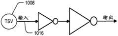
由于在给定晶体管相对于TSV的位置、类型和取向的情况下,可以预先针对特定制造工艺表征由TSV引起的应力对靠近TSV放置的晶体管的影响,因此本发明的一个方面为在单个宏单元中一同包括晶体管和TSV。图10A、图10B和图10C(统称图10)图示了2x输入缓冲器的示例中的某些信息,该2x输入缓冲器可以用于缓冲来自TSV 1008的、用于驱动3D集成器件的特定晶片级上的电路的输入信号。通常许多此类缓冲器并联连接,但是为描述简洁起见而仅在此示出了2x缓冲器。Since the effect of TSV-induced stress on transistors placed close to a TSV can be characterized in advance for a particular fabrication process, given the location, type, and orientation of the transistor relative to the TSV, it is an aspect of the present invention to Include transistors and TSVs together. Figures 10A, 10B, and 10C (collectively, Figure 10) illustrate some of the information in an example of a 2x input buffer that can be used to buffer specific signals from the
图10A图示了宏单元的电路符号,而图10B是宏单元的晶体管级示图。如在图10B中可见,宏单元包括三个P型沟道晶体管T1010P、T1012P和T1014P以及三个N型沟道晶体管T1010N、T1012N和T1014N。TSV 1008连接至晶体管T1010P和T1010N二者的栅极。晶体管T1010P和T1010N的漏极连接在一起并且连接至晶体管T1012P、T1012N、T1014P和T1014N的栅极。晶体管T1012P、T1012N、T1014P和T1014N的漏极全都连接在一起并且形成2x缓冲器宏单元的输出端。三个P型沟道晶体管T1010P、T1012P和T1014P的源极全都连接至POWER导体1024,并且三个N型沟道晶体管T1010N、T1012N和T1014N的源极全都连接至GROUND导体1026。FIG. 10A illustrates a circuit symbol for a macrocell, while FIG. 10B is a transistor-level diagram of a macrocell. As can be seen in FIG. 10B , the macrocell includes three P-channel transistors T1010P, T1012P, and T1014P and three N-channel transistors T1010N, T1012N, and T1014N.
图10C图示了宏单元的版图。(在此的所有版图示图均应被认为是图示在使用版图制成的掩模组上以及在使用版图制成的集成电路器件上存在的特征。)所有的P型沟道晶体管T1010P、T1012P和T1014P都位于P型扩散区1020中,而所有的N型沟道晶体管T1010N、T1012N和T1014N都位于N型扩散1022中。晶体管全都定向成与图中所示的x轴平行,其在图10的实施方式中处于距TSV1008的<110>方向(标准方向)上。然而,如先前所说明,如果2x缓冲器的晶体管过于靠近TSV 1008,则在晶体管的沟道中所引起的应力可能显著改变迁移率。尽管如此,在图10的宏单元中晶体管位于使晶体管沟道载流子迁移率改变5%以上的充分靠近TSV 1008之处。因为还向宏单元提供以将每个晶体管到TSV的距离考虑在内的方式限定电路参数的仿真模型的事实而可能做到这一点。优选地,其还将每个晶体管距x轴的角位移考虑在内,并且优选地还将每个晶体管相对于x轴的取向考虑在内。通过这样的表征,即使2x缓冲器的晶体管位于远比先前被认为是明智的情况更加靠近TSV 1008之处,仍然能够将宏单元用在更大的电路设计中。Figure 10C illustrates the layout of a macrocell. (All layout diagrams herein should be considered to illustrate the features that exist on the mask set made using the layout and on the integrated circuit device made using the layout.) All P-channel transistors T1010P All N-channel transistors T1010N, T1012N and T1014N are located in N-
在图10C中,所有的P型沟道晶体管T1010P、T1012P和T1014P都沿x轴放置并且与x轴纵向地定向。如先前所说明的,可以通过将P型沟道晶体管移动到y轴来提高它们的性能。这在图11的宏单元版图中示出。在图11的实施方式中,所有的P型沟道晶体管现在都定向成与TSV 1008相切,并且被放置在使耦合到沟道中的由TSV引起的压缩应力为最大值的对x轴的角位移处。可以看到,N型沟道晶体管T1010N、T1012N和T1014N也已经被移动到不是最佳的位置和取向,但是如前所述,N型沟道晶体管对由附近TSV所引起的应力的敏感性要小得多。In FIG. 1OC, all of the P-channel transistors T1010P, T1012P, and T1014P are placed along and oriented longitudinally to the x-axis. As previously explained, the performance of P-channel transistors can be improved by moving them to the y-axis. This is shown in the macrocell layout of FIG. 11 . In the embodiment of Figure 11, all P-channel transistors are now oriented tangent to the
还如先前所说明的,可以备选地通过就地旋转P型沟道晶体管以使它们定向成与TSV 1008相切而提高它们的性能。这在图12的宏单元版图中示出。另外如图13的宏单元版图中所示,缓冲器电路可以被放置在距x轴的任何角位移处,并且优选地被定向成相切(或者“基本上”相切)。Also as previously explained, the performance of the P-channel transistors can alternatively be increased by rotating them in situ so that they are oriented tangentially to the
计算机系统computer system
图14是可以用于实现包含本发明各方面的软件的计算机系统1410的简化框图。计算机系统1410通常包括处理器子系统1414,该处理器子系统1414经由总线子系统1412与若干个外围设备进行通信。这些外围设备可以包括存储子系统1424(包括存储器子系统1426和文件存储子系统1428)、用户接口输入设备1422、用户接口输出设备1420以及网络接口子系统1416。输入设备和输出设备允许用户与计算机系统1410进行交互。网络接口子系统1416提供通往外部网络的接口,其包括通往通信网络1418的接口,并且网络接口子系统1416经由通信网络1418耦合至其他计算机系统中相应接口设备。通信网络1418可以包括许多互连的计算机系统以及通信链路。这些通信链路可以是有线链路、光链路、无线链路或者用于信息通信的任何其他机制。虽然在一种实施方式中通信网络1418是因特网,但在其他一些实施方式中通信网络1418可以是任何合适的计算机网络。Figure 14 is a simplified block diagram of a
网络接口的物理硬件组件有时被称为网络接口卡(NIC),但是它们并不必须具有卡的形式:例如,它们可以是直接安装在母板上的集成电路(IC)和连接器的形式,或者在单个集成电路上伴随计算机系统的其他组件一同制造的宏单元的形式。The physical hardware components of a network interface are sometimes referred to as network interface cards (NICs), but they don't have to be in the form of cards: for example, they can be in the form of integrated circuits (ICs) and connectors mounted directly on the motherboard, Or in the form of macrocells fabricated along with other components of a computer system on a single integrated circuit.
用户接口输入设备1422可以包括键盘、诸如鼠标、轨迹球、触摸板或者绘图板之类的指点设备、扫描仪、集成在显示器中的触摸屏、诸如语音识别系统、麦克风之类的音频输入设备以及其他类型的输入设备。总体而言,对术语“输入设备”的使用旨在包括用以向计算机系统1410中或者向计算机网络1418上输入信息的所有可能的设备类型和方式。User
用户接口输出设备1420可以包括显示器子系统、打印机、传真机或者非可视化显示器,比如音频输出设备。显示器子系统可以包括阴极射线管(CRT)、诸如液晶显示器(LCD)之类的平板设备、投影设备或者用于创建可视图像的一些其他机制。显示器子系统还可以比如经由音频输出设备提供非可视化显示。总体而言,对“输出设备”的使用旨在包括从计算机系统1410向用户或向另一机器或计算机系统输出信息的所有可能的设备类型和方式。User
存储子系统1424存储提供本发明某些方面的功能性的基本编程及数据架构。例如,实现图1以及图7至图9中电路仿真器和计算机实现步骤的功能的各种模块可以存储在存储系统1424中。这些软件模块一般由处理器子系统1414所执行。存储在存储子系统1424中的数据架构可以包括任何技术文件、宏单元库、版图文件以及本文所提及的任何其他数据库。注意,在一些实施方式中,这些中的一个或多个可以存储在其他位置但是可由计算机系统1410例如经由通信网络1418进行访问。
存储器子系统1426通常包括若干个存储器,其包括用于在程序执行期间存储指令及数据的主随机访问存储器(RAM)1430,以及在其中存储固化指令的只读存储器(ROM)1432。文件存储子系统1428为程序及数据文件提供持久性存储,并且可以包括硬盘驱动器、软盘驱动器连同相关联的可移动介质、CD ROM驱动器、光驱动器或者可移动介质盒。实现本发明某些实施方式的功能的数据库和模块可能已被提供在诸如一个或多个CD-ROM之类的计算机可读介质上(或者可能已经由通信网络1418被传输至计算机系统1410),并且可能由文件存储子系统1428所存储。主机存储器1426包含但不限于当由处理器子系统1414执行时使计算机系统如本文所描述那样工作或执行功能的计算机指令。如本文中所使用,被称为在“主机”或“计算机”中或“主机”或“计算机”上运行的过程和软件响应于主机存储器子系统1426中的计算机指令和数据而在处理器子系统1414上执行,该主机存储器子系统1426包括用于此类指令和数据的任何其他本地或远程存储。
总线子系统1412提供用于让计算机系统1410的各种组件及子系统按照预期彼此进行通信的机制。虽然总线子系统1412被示意性地示为单一总线,但是总线子系统的备选实施方式可以使用多个总线。
计算机系统1410本身可以是包括个人计算机、便携式计算机、工作站、计算机终端、网络计算机、电视机、大型机或者任何其他数据处理系统或用户设备在内的不同类型。由于计算机和网络的不断变化的性质,因此对图14中所描绘的计算机系统1410的描述旨在仅作为用于说明本发明优选实施方式目的的特定示例。计算机系统1410的比图14中所描绘的计算机系统具有更多或更少组件的许多其他配置都是可能的。
如本文中所使用的,对信息项的“标识”并不一定要求对该信息项的直接指定。信息可以在字段中通过简单地经过一个或多个层次的间接迂回来引用实际信息,或者通过对一起足以用于确定实际信息项的不同信息的一个或多个项进行标识而“被标识”。此外,在此所使用的术语“指示”的意思与“标识”相同。As used herein, "identification" of an item of information does not necessarily require direct designation of the item of information. Information may be "identified" in a field by simply referencing the actual information through one or more levels of indirection, or by identifying one or more items of distinct information that together are sufficient to determine the actual item of information. In addition, the term "indicate" used herein has the same meaning as "identify".
并且如本文中所使用的,如果前驱值影响到给定值,则该给定值“响应”于该前驱值。如果存在中间处理元素、步骤或时段,则该给定值仍然可以“响应”于前驱值。如果中间处理元素或步骤结合了不止一个值,则处理元素或步骤的输出被认为是“响应”于每个值输入。如果给定值与前驱值相同,则这仅仅是一种简并情况,在其中给定值仍被认为是“响应”于前驱值。给定值对于另一值的“依赖性”以类似方式定义。And as used herein, a given value is "responsive" to a precursor value if the precursor value affects the given value. If there are intermediate processing elements, steps or periods, the given value can still "respond" to the predecessor value. If an intermediate processing element or step incorporates more than one value, the output of the processing element or step is said to be "responsive" to each value input. If the given value is the same as the predecessor value, this is only a degenerate case in which the given value is still considered to be "responsive" to the predecessor value. The "dependence" of a given value on another value is defined in a similar manner.
已经出于说明及描述的目的而提供了本发明优选实施方式的前文描述。其并不旨在称为穷尽性或者将本发明限于所公开的精确形式。明显地,许多修改和变形对于本领域中从业人员都将是显而易见的。具体地但非限制性地而言,在本专利申请的背景技术部分中所描述、建议或者通过引用并入其中的任何及全部变形均明确地通过引用而并入本发明实施方式在此的描述之中。在此所描述的实施方式被选择及描述用以最好地解释本发明的原理及其实际应用,从而使本领域中技术人员能够针对各种实施方式并且伴随适合于所设想的特定用途的各种修改而理解本发明。本发明的范围旨在由以下权利要求及其等同条款所限定。The foregoing description of the preferred embodiment of the invention has been presented for purposes of illustration and description. It is not intended to be exhaustive or to limit the invention to the precise forms disclosed. Obviously, many modifications and variations will be apparent to those skilled in the art. In particular, but not limitation, any and all variations described, suggested, or incorporated by reference in the Background section of this patent application are expressly incorporated by reference into the description herein of the embodiments of the invention among. The embodiments described herein were chosen and described in order to best explain the principles of the invention and its practical application, thereby enabling others skilled in the art to ascertain the various embodiments and accompany the various embodiments as are suited to the particular use contemplated. modifications to understand the invention. It is intended that the scope of the invention be defined by the following claims and their equivalents.
Claims (25)
Applications Claiming Priority (3)
| Application Number | Priority Date | Filing Date | Title |
|---|---|---|---|
| US12/430,008 | 2009-04-24 | ||
| US12/430,008US8362622B2 (en) | 2009-04-24 | 2009-04-24 | Method and apparatus for placing transistors in proximity to through-silicon vias |
| PCT/US2010/029326WO2010123659A2 (en) | 2009-04-24 | 2010-03-31 | Method and apparatus for placing transistors in proximity to through-silicon vias |
Publications (2)
| Publication Number | Publication Date |
|---|---|
| CN102414684Atrue CN102414684A (en) | 2012-04-11 |
| CN102414684B CN102414684B (en) | 2014-02-12 |
Family
ID=42991345
Family Applications (1)
| Application Number | Title | Priority Date | Filing Date |
|---|---|---|---|
| CN201080017985.9AActiveCN102414684B (en) | 2009-04-24 | 2010-03-31 | Method and apparatus for placing transistors adjacent to silicon vias |
Country Status (5)
| Country | Link |
|---|---|
| US (4) | US8362622B2 (en) |
| EP (1) | EP2422287B8 (en) |
| CN (1) | CN102414684B (en) |
| TW (1) | TWI423059B (en) |
| WO (1) | WO2010123659A2 (en) |
Cited By (8)
| Publication number | Priority date | Publication date | Assignee | Title |
|---|---|---|---|---|
| CN102663204A (en)* | 2012-04-25 | 2012-09-12 | 北京工业大学 | Distance optimizing method of through silicon via (TSV) positions in three-dimensional (3D) integrated circuit automatic layout |
| CN104471714A (en)* | 2012-06-13 | 2015-03-25 | 美商新思科技有限公司 | N-channel and P-channel end-to-end FinFET cell architecture |
| CN104600076A (en)* | 2013-10-31 | 2015-05-06 | 骆志炯 | Connecting storage grid storing unit, operation and manufacturing method thereof |
| CN106556790A (en)* | 2015-09-24 | 2017-04-05 | 中芯国际集成电路制造(上海)有限公司 | A kind of silicon hole sensor and detection method, electronic installation |
| CN107483150A (en)* | 2017-08-10 | 2017-12-15 | 北京信息科技大学 | Channel concatenated code encoding method and signal transmission method and device based on TSV transmission |
| CN108027845A (en)* | 2015-08-03 | 2018-05-11 | 美商新思科技有限公司 | Design rule is assessed before silicon |
| CN110196984A (en)* | 2018-12-06 | 2019-09-03 | 西安电子科技大学 | A kind of high-speed broadband band modeling method, system, device and storage medium |
| CN111967216A (en)* | 2020-08-25 | 2020-11-20 | 上海华力集成电路制造有限公司 | Method for on-line monitoring transistor size |
Families Citing this family (44)
| Publication number | Priority date | Publication date | Assignee | Title |
|---|---|---|---|---|
| US8082537B1 (en)* | 2009-01-28 | 2011-12-20 | Xilinx, Inc. | Method and apparatus for implementing spatially programmable through die vias in an integrated circuit |
| US7989959B1 (en) | 2009-01-29 | 2011-08-02 | Xilinx, Inc. | Method of forming stacked-die integrated circuit |
| US8987868B1 (en) | 2009-02-24 | 2015-03-24 | Xilinx, Inc. | Method and apparatus for programmable heterogeneous integration of stacked semiconductor die |
| US8362622B2 (en)* | 2009-04-24 | 2013-01-29 | Synopsys, Inc. | Method and apparatus for placing transistors in proximity to through-silicon vias |
| US8264065B2 (en)* | 2009-10-23 | 2012-09-11 | Synopsys, Inc. | ESD/antenna diodes for through-silicon vias |
| US9015023B2 (en) | 2010-05-05 | 2015-04-21 | Xilinx, Inc. | Device specific configuration of operating voltage |
| WO2012077280A1 (en)* | 2010-12-09 | 2012-06-14 | パナソニック株式会社 | Design support device and design support method for three-dimensional integrated circuit |
| US8753981B2 (en) | 2011-04-22 | 2014-06-17 | Micron Technology, Inc. | Microelectronic devices with through-silicon vias and associated methods of manufacturing |
| KR101828063B1 (en)* | 2011-05-17 | 2018-02-09 | 삼성전자주식회사 | Semiconductor device and method of forming the same |
| US8779553B2 (en)* | 2011-06-16 | 2014-07-15 | Xilinx, Inc. | Stress-aware design for integrated circuits comprising a stress inducing structure and keep out zone |
| US8560982B2 (en) | 2011-06-27 | 2013-10-15 | Xilinx, Inc. | Integrated circuit design using through silicon vias |
| US8990760B2 (en)* | 2011-08-26 | 2015-03-24 | Mentor Graphics Corporation | Cell-aware fault model generation for delay faults |
| US8448124B2 (en) | 2011-09-20 | 2013-05-21 | International Business Machines Corporation | Post timing layout modification for performance |
| CN103094252B (en)* | 2011-10-31 | 2015-04-29 | 中芯国际集成电路制造(上海)有限公司 | Through-silicon via (TSV) testing structure and TSV testing method |
| US8887106B2 (en) | 2011-12-28 | 2014-11-11 | Taiwan Semiconductor Manufacturing Company, Ltd. | Method of generating a bias-adjusted layout design of a conductive feature and method of generating a simulation model of a predefined fabrication process |
| US8903698B2 (en)* | 2012-05-15 | 2014-12-02 | Fujitsu Limited | Generating behavioral models for analog circuits |
| US20140003632A1 (en)* | 2012-06-28 | 2014-01-02 | Ams Ag | Microphone arrangement |
| US8555225B1 (en)* | 2012-08-08 | 2013-10-08 | Apple Inc. | Hierarchical stress parameter annotation |
| US8776005B1 (en) | 2013-01-18 | 2014-07-08 | Synopsys, Inc. | Modeling mechanical behavior with layout-dependent material properties |
| US9653615B2 (en)* | 2013-03-13 | 2017-05-16 | International Business Machines Corporation | Hybrid ETSOI structure to minimize noise coupling from TSV |
| US9030025B2 (en) | 2013-03-15 | 2015-05-12 | IPEnval Consultant Inc. | Integrated circuit layout |
| US8957504B2 (en) | 2013-03-15 | 2015-02-17 | IP Enval Consultant Inc. | Integrated structure with a silicon-through via |
| US8952500B2 (en) | 2013-03-15 | 2015-02-10 | IPEnval Consultant Inc. | Semiconductor device |
| FR3003973A1 (en)* | 2013-03-26 | 2014-10-03 | Commissariat Energie Atomique | METHOD FOR GENERATING MODELING FILES OF INTEGRATED CIRCUIT DESIGN FLOT, COMPUTER PROGRAM AND CORRESPONDING SYSTEM |
| US9000490B2 (en) | 2013-04-19 | 2015-04-07 | Xilinx, Inc. | Semiconductor package having IC dice and voltage tuners |
| TWI538174B (en)* | 2013-09-25 | 2016-06-11 | 晶相光電股份有限公司 | Semiconductor device manufacturing method |
| US9891261B2 (en) | 2014-06-30 | 2018-02-13 | International Business Machines Corporation | Electromigration monitor |
| US9501603B2 (en) | 2014-09-05 | 2016-11-22 | International Business Machines Corporation | Integrated circuit design changes using through-silicon vias |
| US9553054B2 (en) | 2014-10-23 | 2017-01-24 | Globalfoundries Inc. | Strain detection structures for bonded wafers and chips |
| US9859192B2 (en)* | 2015-03-12 | 2018-01-02 | Mediatek Inc. | Semiconductor structure with through-silicon via |
| JP2017041529A (en)* | 2015-08-19 | 2017-02-23 | 富士通株式会社 | Semiconductor device and manufacturing method thereof |
| KR102400557B1 (en)* | 2015-10-13 | 2022-05-20 | 삼성전자주식회사 | Circuit Design Method and Simulation Method considering random telegraph signal noise |
| US9959380B2 (en)* | 2016-03-28 | 2018-05-01 | Motivo, Inc. | Integrated circuit design systems and methods |
| US10936778B2 (en) | 2016-03-28 | 2021-03-02 | Motivo, Inc. | And optimization of physical cell placement |
| US10572615B2 (en)* | 2017-04-28 | 2020-02-25 | Synopsys, Inc. | Placement and routing of cells using cell-level layout-dependent stress effects |
| KR102337647B1 (en) | 2017-05-17 | 2021-12-08 | 삼성전자주식회사 | Semiconductor package and method for fabricating the same |
| KR102374111B1 (en) | 2017-08-21 | 2022-03-14 | 삼성전자주식회사 | System and method of manufacturing image sensor |
| US10298420B1 (en) | 2018-03-20 | 2019-05-21 | Dell Products, Lp | System and method to enhance feed-forward equalization in a high-speed serial interface |
| JP2020197667A (en) | 2019-06-04 | 2020-12-10 | キオクシア株式会社 | Pattern generator, pattern generation method and manufacturing method of semiconductor device |
| US11080460B2 (en) | 2019-10-14 | 2021-08-03 | Samsung Electronics Co., Ltd. | Method of modeling high speed channel in semiconductor package, method of designing semiconductor package using the same and method of manufacturing semiconductor package using the same |
| CN111062145B (en)* | 2019-12-30 | 2022-03-11 | 浙江大学 | An Equivalent Method for Electromagnetic Transient Simulation Based on Three-layer Partitioning and Electrical Distance |
| US11080455B1 (en)* | 2020-07-09 | 2021-08-03 | Taiwan Semiconductor Manufacturing Company, Ltd. | Layout design of integrated circuit with through-substrate via |
| KR102819717B1 (en) | 2020-07-31 | 2025-06-12 | 삼성전자주식회사 | Semiconductor device and method of designing semiconductor device |
| US12382724B2 (en)* | 2021-05-28 | 2025-08-05 | Taiwan Semiconductor Manufacturing Company Ltd. | Layout design for header cell in 3D integrated circuits |
Citations (3)
| Publication number | Priority date | Publication date | Assignee | Title |
|---|---|---|---|---|
| CN101295693A (en)* | 2007-04-24 | 2008-10-29 | 恩益禧电子股份有限公司 | Semiconductor device |
| CN101322241A (en)* | 2005-11-29 | 2008-12-10 | 富士通株式会社 | Semiconductor device and method for manufacturing the same |
| US20090102021A1 (en)* | 2007-10-17 | 2009-04-23 | Chih-Hua Chen | Through-Silicon Vias and Methods for Forming the Same |
Family Cites Families (32)
| Publication number | Priority date | Publication date | Assignee | Title |
|---|---|---|---|---|
| US6557150B1 (en)* | 1997-08-20 | 2003-04-29 | Hitachi, Ltd. | Method of extracting timing characteristics of transistor circuits, storage medium storing timing characteristic library, LSI designing method, and gate extraction method |
| US6826517B2 (en) | 2000-12-21 | 2004-11-30 | Kabushiki Kaisha Toshiba | Method and apparatus for simulating manufacturing, electrical and physical characteristics of a semiconductor device |
| US6492224B1 (en) | 2001-07-16 | 2002-12-10 | Taiwan Semiconductor Manufacturing Company | Buried PIP capacitor for mixed-mode process |
| JP4408613B2 (en)* | 2002-09-25 | 2010-02-03 | Necエレクトロニクス株式会社 | Circuit simulation apparatus incorporating transistor diffusion layer length dependency and transistor model creation method |
| US7032194B1 (en) | 2003-02-19 | 2006-04-18 | Xilinx, Inc. | Layout correction algorithms for removing stress and other physical effect induced process deviation |
| US6845034B2 (en) | 2003-03-11 | 2005-01-18 | Micron Technology, Inc. | Electronic systems, constructions for detecting properties of objects, and assemblies for identifying persons |
| JPWO2004112139A1 (en) | 2003-06-10 | 2006-09-28 | 富士通株式会社 | Semiconductor device and manufacturing method thereof |
| US7495296B2 (en) | 2004-06-01 | 2009-02-24 | Panasonic Corporation | Semiconductor integrated circuit device |
| US7190036B2 (en) | 2004-12-03 | 2007-03-13 | Taiwan Semiconductor Manufacturing Company, Ltd. | Transistor mobility improvement by adjusting stress in shallow trench isolation |
| US7266787B2 (en) | 2005-02-24 | 2007-09-04 | Icera, Inc. | Method for optimising transistor performance in integrated circuits |
| JP4515951B2 (en) | 2005-03-31 | 2010-08-04 | 富士通セミコンダクター株式会社 | Semiconductor device and manufacturing method thereof |
| CN102610606B (en)* | 2005-04-26 | 2016-01-27 | 瑞萨电子株式会社 | Semiconductor device and manufacture method, optical proximity processing method |
| US7476938B2 (en) | 2005-11-21 | 2009-01-13 | International Business Machines Corporation | Transistor having dielectric stressor elements at different depths from a semiconductor surface for applying shear stress |
| US7767515B2 (en) | 2006-02-27 | 2010-08-03 | Synopsys, Inc. | Managing integrated circuit stress using stress adjustment trenches |
| US7600207B2 (en) | 2006-02-27 | 2009-10-06 | Synopsys, Inc. | Stress-managed revision of integrated circuit layouts |
| US7484198B2 (en) | 2006-02-27 | 2009-01-27 | Synopsys, Inc. | Managing integrated circuit stress using dummy diffusion regions |
| US7776726B2 (en)* | 2006-05-04 | 2010-08-17 | Infineon Technologies Ag | Semiconductor devices and methods of manufacture thereof |
| US7671421B2 (en)* | 2006-05-31 | 2010-03-02 | International Business Machines Corporation | CMOS structure and method for fabrication thereof using multiple crystallographic orientations and gate materials |
| US7542891B2 (en)* | 2006-09-07 | 2009-06-02 | Synopsys, Inc. | Method of correlating silicon stress to device instance parameters for circuit simulation |
| WO2008085926A1 (en)* | 2007-01-04 | 2008-07-17 | Supresta Llc | Phosphoramide ester flame retardant and resins containing same |
| US7494846B2 (en) | 2007-03-09 | 2009-02-24 | Taiwan Semiconductor Manufacturing Company, Ltd. | Design techniques for stacking identical memory dies |
| US8046727B2 (en) | 2007-09-12 | 2011-10-25 | Neal Solomon | IP cores in reconfigurable three dimensional integrated circuits |
| KR101519440B1 (en) | 2007-10-04 | 2015-05-13 | 삼성전자주식회사 | Stacked semiconductor apparatus with configurable vertical i/o and methos there-of |
| US7968460B2 (en)* | 2008-06-19 | 2011-06-28 | Micron Technology, Inc. | Semiconductor with through-substrate interconnect |
| US7888668B2 (en)* | 2008-07-17 | 2011-02-15 | United Microelectronics Corp. | Phase change memory |
| US8138036B2 (en)* | 2008-08-08 | 2012-03-20 | International Business Machines Corporation | Through silicon via and method of fabricating same |
| US20100052174A1 (en)* | 2008-08-27 | 2010-03-04 | Agere Systems Inc. | Copper pad for copper wire bonding |
| US7846837B2 (en)* | 2008-10-09 | 2010-12-07 | United Microelectronics Corp. | Through substrate via process |
| US7964502B2 (en)* | 2008-11-25 | 2011-06-21 | Freescale Semiconductor, Inc. | Multilayered through via |
| US8299583B2 (en)* | 2009-03-05 | 2012-10-30 | International Business Machines Corporation | Two-sided semiconductor structure |
| US8169055B2 (en)* | 2009-03-18 | 2012-05-01 | International Business Machines Corporation | Chip guard ring including a through-substrate via |
| US8362622B2 (en) | 2009-04-24 | 2013-01-29 | Synopsys, Inc. | Method and apparatus for placing transistors in proximity to through-silicon vias |
- 2009
- 2009-04-24USUS12/430,008patent/US8362622B2/enactiveActive
- 2010
- 2010-03-31WOPCT/US2010/029326patent/WO2010123659A2/enactiveApplication Filing
- 2010-03-31CNCN201080017985.9Apatent/CN102414684B/enactiveActive
- 2010-03-31EPEP10767488.9Apatent/EP2422287B8/enactiveActive
- 2010-04-23TWTW099112954Apatent/TWI423059B/enactive
- 2013
- 2013-01-14USUS13/740,439patent/US8661387B2/enactiveActive
- 2014
- 2014-02-24USUS14/188,532patent/US9003348B2/enactiveActive
- 2015
- 2015-03-31USUS14/674,462patent/US9275182B2/enactiveActive
Patent Citations (3)
| Publication number | Priority date | Publication date | Assignee | Title |
|---|---|---|---|---|
| CN101322241A (en)* | 2005-11-29 | 2008-12-10 | 富士通株式会社 | Semiconductor device and method for manufacturing the same |
| CN101295693A (en)* | 2007-04-24 | 2008-10-29 | 恩益禧电子股份有限公司 | Semiconductor device |
| US20090102021A1 (en)* | 2007-10-17 | 2009-04-23 | Chih-Hua Chen | Through-Silicon Vias and Methods for Forming the Same |
Non-Patent Citations (1)
| Title |
|---|
| MICHAEL W.NEWMAN ETC: "Fabrication and Electrical Characterization of 3D Vertical Interconnects", 《2006 ELECTRONIC COMPONENTS AND TECHNOLOGY CONFERENCE》, 30 December 2006 (2006-12-30)* |
Cited By (14)
| Publication number | Priority date | Publication date | Assignee | Title |
|---|---|---|---|---|
| CN102663204B (en)* | 2012-04-25 | 2014-03-26 | 北京工业大学 | Distance optimizing method of through silicon via (TSV) positions in three-dimensional (3D) integrated circuit automatic layout |
| CN102663204A (en)* | 2012-04-25 | 2012-09-12 | 北京工业大学 | Distance optimizing method of through silicon via (TSV) positions in three-dimensional (3D) integrated circuit automatic layout |
| CN104471714A (en)* | 2012-06-13 | 2015-03-25 | 美商新思科技有限公司 | N-channel and P-channel end-to-end FinFET cell architecture |
| US9646966B2 (en) | 2012-06-13 | 2017-05-09 | Synopsys, Inc. | N-channel and P-channel end-to-end finFET cell architecture |
| CN104600076A (en)* | 2013-10-31 | 2015-05-06 | 骆志炯 | Connecting storage grid storing unit, operation and manufacturing method thereof |
| CN104600076B (en)* | 2013-10-31 | 2018-05-11 | 骆志炯 | Connection storage grid storage unit and its operation and manufacture method |
| CN108027845B (en)* | 2015-08-03 | 2021-07-02 | 美商新思科技有限公司 | Pre-silicon design rule evaluation |
| CN108027845A (en)* | 2015-08-03 | 2018-05-11 | 美商新思科技有限公司 | Design rule is assessed before silicon |
| CN106556790A (en)* | 2015-09-24 | 2017-04-05 | 中芯国际集成电路制造(上海)有限公司 | A kind of silicon hole sensor and detection method, electronic installation |
| CN107483150A (en)* | 2017-08-10 | 2017-12-15 | 北京信息科技大学 | Channel concatenated code encoding method and signal transmission method and device based on TSV transmission |
| CN110196984B (en)* | 2018-12-06 | 2020-12-29 | 西安电子科技大学 | A high-speed broadband modeling method, system, device and storage medium |
| CN110196984A (en)* | 2018-12-06 | 2019-09-03 | 西安电子科技大学 | A kind of high-speed broadband band modeling method, system, device and storage medium |
| CN111967216A (en)* | 2020-08-25 | 2020-11-20 | 上海华力集成电路制造有限公司 | Method for on-line monitoring transistor size |
| CN111967216B (en)* | 2020-08-25 | 2023-11-14 | 上海华力集成电路制造有限公司 | Method for on-line monitoring transistor size |
Also Published As
| Publication number | Publication date |
|---|---|
| US8362622B2 (en) | 2013-01-29 |
| US20130132914A1 (en) | 2013-05-23 |
| EP2422287A4 (en) | 2015-07-22 |
| US8661387B2 (en) | 2014-02-25 |
| US9275182B2 (en) | 2016-03-01 |
| TW201109961A (en) | 2011-03-16 |
| WO2010123659A3 (en) | 2011-01-13 |
| TWI423059B (en) | 2014-01-11 |
| EP2422287B1 (en) | 2020-05-20 |
| US9003348B2 (en) | 2015-04-07 |
| US20150205904A1 (en) | 2015-07-23 |
| EP2422287A2 (en) | 2012-02-29 |
| WO2010123659A2 (en) | 2010-10-28 |
| CN102414684B (en) | 2014-02-12 |
| US20100270597A1 (en) | 2010-10-28 |
| EP2422287B8 (en) | 2020-07-01 |
| US20140173545A1 (en) | 2014-06-19 |
Similar Documents
| Publication | Publication Date | Title |
|---|---|---|
| US9275182B2 (en) | Placing transistors in proximity to through-silicon vias | |
| KR102396699B1 (en) | Cell placement and routing using cell level layout dependent stress effects | |
| US8086990B2 (en) | Method of correlating silicon stress to device instance parameters for circuit simulation | |
| US10606968B2 (en) | Atomic scale grid for modeling semiconductor structures and fabrication processes | |
| US10482212B2 (en) | Automated resistance and capacitance extraction and netlist generation of logic cells | |
| US7996795B2 (en) | Method and apparatus for performing stress modeling of integrated circuit material undergoing material conversion | |
| US20170161425A1 (en) | Compact modeling analysis of circuit layout shape sections | |
| US20160162625A1 (en) | Mapping Intermediate Material Properties To Target Properties To Screen Materials | |
| US20180144073A1 (en) | Modeling Deformation Due To Surface Oxidation In Integrated Circuits | |
| TW202018870A (en) | Method and system of developing statistical model | |
| US11727186B2 (en) | Automatic identification of hierarchical cells based on selected properties for layout verification | |
| Cai et al. | A transistor sizing method for standard-cell optimization considering lithography effects | |
| Acar et al. | Examination of process parameter variations | |
| Atluri | Design Automation Flow using Library Adaptation for Variation Aware Logic Synthesis | |
| Saha et al. | Improving yield in advanced technologies by modeling variability. |
Legal Events
| Date | Code | Title | Description |
|---|---|---|---|
| C06 | Publication | ||
| PB01 | Publication | ||
| C10 | Entry into substantive examination | ||
| SE01 | Entry into force of request for substantive examination | ||
| C14 | Grant of patent or utility model | ||
| GR01 | Patent grant |