CN102412242B - Light-emitting diode (LED) chipset capable of being connected to alternating current directly - Google Patents
Light-emitting diode (LED) chipset capable of being connected to alternating current directlyDownload PDFInfo
- Publication number
- CN102412242B CN102412242BCN 201110375793CN201110375793ACN102412242BCN 102412242 BCN102412242 BCN 102412242BCN 201110375793CN201110375793CN 201110375793CN 201110375793 ACN201110375793 ACN 201110375793ACN 102412242 BCN102412242 BCN 102412242B
- Authority
- CN
- China
- Prior art keywords
- layer
- light
- emitting diode
- type
- electrode
- Prior art date
- Legal status (The legal status is an assumption and is not a legal conclusion. Google has not performed a legal analysis and makes no representation as to the accuracy of the status listed.)
- Expired - Fee Related
Links
- 239000004065semiconductorSubstances0.000claimsabstractdescription74
- 239000010410layerSubstances0.000claimsdescription193
- 239000002184metalSubstances0.000claimsdescription64
- 229910052751metalInorganic materials0.000claimsdescription64
- 229920002120photoresistant polymerPolymers0.000claimsdescription57
- 230000015572biosynthetic processEffects0.000claimsdescription15
- 238000002955isolationMethods0.000claimsdescription14
- 239000000463materialSubstances0.000claimsdescription12
- 229910001092metal group alloyInorganic materials0.000claimsdescription8
- 239000000758substrateSubstances0.000claimsdescription7
- 229910002601GaNInorganic materials0.000claimsdescription3
- 238000005530etchingMethods0.000claimsdescription3
- 229910052594sapphireInorganic materials0.000claimsdescription3
- 239000010980sapphireSubstances0.000claimsdescription3
- HBMJWWWQQXIZIP-UHFFFAOYSA-Nsilicon carbideChemical compound[Si+]#[C-]HBMJWWWQQXIZIP-UHFFFAOYSA-N0.000claimsdescription3
- 229910010271silicon carbideInorganic materials0.000claimsdescription3
- 239000012790adhesive layerSubstances0.000claimsdescription2
- 230000010354integrationEffects0.000abstract7
- 238000004519manufacturing processMethods0.000description27
- 238000010586diagramMethods0.000description24
- XEEYBQQBJWHFJM-UHFFFAOYSA-NIronChemical compound[Fe]XEEYBQQBJWHFJM-UHFFFAOYSA-N0.000description10
- 239000011248coating agentSubstances0.000description8
- 238000000576coating methodMethods0.000description8
- 229910052742ironInorganic materials0.000description5
- 238000000034methodMethods0.000description3
- 238000001704evaporationMethods0.000description2
- 230000008020evaporationEffects0.000description2
- 238000004544sputter depositionMethods0.000description2
- 230000009286beneficial effectEffects0.000description1
- 239000008358core componentSubstances0.000description1
- 238000004020luminiscence typeMethods0.000description1
- 229910021421monocrystalline siliconInorganic materials0.000description1
- 230000006798recombinationEffects0.000description1
- 238000005215recombinationMethods0.000description1
Images


Landscapes
- Led Devices (AREA)
Abstract
Description
Translated fromChinese技术领域technical field
本发明涉及一种发光二极管芯片,尤其是涉及一种可直接连接在交流电上的LED芯片组。The invention relates to a light-emitting diode chip, in particular to an LED chip group which can be directly connected to an alternating current.
背景技术Background technique
发光二极管芯片,是led灯的核心组件,也就是指的P-N结。其主要功能是:把电能转化为光能,芯片的主要材料为单晶硅。半导体晶片由两部分组成,一部分是P型半导体,在它里面空穴占主导地位,另一端是N型半导体,在这边主要是电子。但这两种半导体连接起来的时候,它们之间就形成一个P-N结。当电流通过导线作用于这个晶片的时候,电子就会被推向P区,在P区里电子跟空穴复合,然后就会以光子的形式发出能量,这就是LED发光的原理。而光的波长也就是光的颜色,是由形成P-N结的材料决定的。 The light-emitting diode chip is the core component of the LED lamp, which refers to the P-N junction. Its main function is to convert electrical energy into light energy, and the main material of the chip is monocrystalline silicon. Semiconductor wafer is made up of two parts, and a part is P-type semiconductor, and hole occupies an leading position in it, and the other end is N-type semiconductor, and here mainly is electron. But time these two kinds of semiconductors couple together, between them, just form a P-N junction. When electric current acts on this chip by wire time, electron will be pushed to P district, and in P district, electron is with hole recombination, then will send energy with the form of photon, the principle of LED luminescence that Here it is. And the wavelength of light i.e. the color of light, be determined by the material forming P-N junction. the
发光二极管芯片的P-N结具有单向导电性:即正向导通,反向不导通。对红黄光发光二极管,其正向导通电压在2伏左右,而对蓝绿光二极管,正向导通电压在3.0伏左右。当二极管的正向电压高于导通电压后,流过二极管的电流将随着外加电压的增加而迅速增加;当流过二极管的电流过大时,由于二极管本身产生的热量过大而可能被烧毁。目前,一般1瓦蓝光二极管的工作电流在350毫安左右,相应的工作电压远小于4伏。显然,一般二极管由于其单向导通性和较低的工作电压限制。由此可见,所有的发光二极管芯片使用都需要额外设置的整流电路和外加电阻配合使用,因而会增加了灯具生产成本以及电路连接的复杂性。The P-N junction of the light-emitting diode chip has unidirectional conductivity: that is, it conducts in the forward direction and does not conduct in the reverse direction. For red and yellow light emitting diodes, the forward conducting voltage is about 2 volts, while for blue and green light emitting diodes, the forward conducting voltage is about 3.0 volts. When the forward voltage of the diode is higher than the conduction voltage, the current flowing through the diode will increase rapidly with the increase of the applied voltage; when the current flowing through the diode is too large, it may be burned due to the excessive heat generated by the diode itself burn. At present, the operating current of a general 1-watt blue light diode is about 350 mA, and the corresponding operating voltage is far less than 4 volts. Obviously, general diodes are limited due to their unidirectional conductivity and lower operating voltage. It can be seen that all light-emitting diode chips need an additional rectifier circuit and an external resistor to be used together, which will increase the production cost of the lamp and the complexity of the circuit connection.
此外,现有LED芯片是无法与交流电直接连接使用的,需要增加额外设施。In addition, existing LED chips cannot be directly connected to AC power, and additional facilities need to be added.
发明内容Contents of the invention
本发明设计了一种可直接连接在交流电上的LED芯片组,其解决的技术问题是(1)现有LED芯片组无法直接与交流电直接使用;(2)现有发光二极管芯片需要与专门的整流电路和外加电阻配合使用,会增加了灯具生产成本以及电路连接的复杂性。The present invention designs an LED chip set that can be directly connected to AC power, and the technical problems it solves are (1) The existing LED chip set cannot be directly used with AC power; The combined use of the rectifier circuit and the external resistor will increase the production cost of the lamp and the complexity of the circuit connection.
为了解决上述存在的技术问题,本发明采用了以下方案:In order to solve the above-mentioned technical problems, the present invention adopts the following scheme:
一种可直接连接在交流电上的LED芯片组,至少包括两枚集成电阻发光二极管芯片,所述两枚集成电阻发光二极管芯片并联在交流电正负极,每一枚集成电阻发光二极管芯片包括第一半导体电阻(R1)和第二半导体电阻(R2),在所述第一半导体电阻(R1)和所述第二半导体电阻(R2)之间串联有多个发光二极管(L1、L2、L3),所述多个发光二极管(L1、L2、L3)的PN结走向相同,根据二极管正向导通原理两枚集成电阻发光二极管芯片在交流电作用下交替发光。An LED chip set that can be directly connected to an alternating current, comprising at least two integrated resistor light emitting diode chips, the two integrated resistor light emitting diode chips are connected in parallel to the positive and negative poles of the alternating current, each integrated resistor light emitting diode chip includes a first A semiconductor resistor (R1) and a second semiconductor resistor (R2), a plurality of light-emitting diodes (L1, L2, L3) are connected in series between the first semiconductor resistor (R1) and the second semiconductor resistor (R2), The PN junctions of the plurality of light emitting diodes (L1, L2, L3) have the same direction, and the two integrated resistor light emitting diode chips alternately emit light under the action of alternating current according to the principle of diode forward conduction.
进一步,一枚集成电阻发光二极管芯片的第一半导体电阻(R1)和另一枚集成电阻发光二极管芯片的第二半导体电阻(R2)的连接端与交流电正极或负极直接连接。Further, the connecting end of the first semiconductor resistor (R1) of one integrated resistor LED chip and the second semiconductor resistor (R2) of the other integrated resistor LED chip is directly connected to the anode or cathode of the alternating current.
进一步,所述第一半导体电阻(R1)、所述第二半导体电阻(R2)以及所述多个发光二极管除了共用一衬底(1)层外分别由独立的缓冲层(2)、N型层(3)、N型分别限制层(4)、有源区结构(5)、P型分别限制层(6)、P型层(7)、P型欧姆接触层(8)以及P型金属欧姆接触层(9)由下至上组合而成;相邻两个发光二极管通过N型层(3)电极与P型金属欧姆接触层(9)电极连接实现串联;所述第一半导体电阻(R1)和所述第二半导体电阻(R2)分别都设有两个接触电极,所述第一半导体电阻(R1)或所述第二半导体电阻(R2)的一个接触电极与电源的正极或负极连接,另外一个接触电极与相邻发光二极管的N型层(3)或P型金属欧姆接触层(9)连接。Further, the first semiconductor resistor (R1), the second semiconductor resistor (R2) and the plurality of light-emitting diodes are respectively composed of an independent buffer layer (2), an N-type Layer (3), N-type respectively confinement layer (4), active region structure (5), P-type respectively confinement layer (6), P-type layer (7), P-type ohmic contact layer (8) and P-type metal The ohmic contact layer (9) is formed from bottom to top; two adjacent light-emitting diodes are connected in series through the electrodes of the N-type layer (3) and the electrodes of the P-type metal ohmic contact layer (9); the first semiconductor resistor (R1 ) and the second semiconductor resistor (R2) are respectively provided with two contact electrodes, and one contact electrode of the first semiconductor resistor (R1) or the second semiconductor resistor (R2) is connected to the positive or negative pole of the power supply , the other contact electrode is connected to the N-type layer (3) or the P-type metal ohmic contact layer (9) of the adjacent light-emitting diode.
进一步,所述第一半导体电阻(R1)、所述第二半导体电阻(R2)以及多个发光二极管的外表都包裹一层绝缘介质膜(13),但多个发光二极管的N型层(3)电极、多个发光二极管的P型金属欧姆接触层(9)电极以及所述第一半导体电阻(R1)和所述第二半导体电阻(R2)的各自两个接触电极上方的绝缘介质膜(13)都去除。Further, the first semiconductor resistor (R1), the second semiconductor resistor (R2) and the plurality of light-emitting diodes are all wrapped with a layer of insulating dielectric film (13), but the N-type layer (3) of the plurality of light-emitting diodes ) electrodes, P-type metal ohmic contact layer (9) electrodes of multiple light-emitting diodes, and the insulating dielectric film above the respective two contact electrodes of the first semiconductor resistor (R1) and the second semiconductor resistor (R2) ( 13) Both are removed.
进一步,所述第一半导体电阻(R1)的P型金属欧姆接触层(9)被P型金属欧姆接触层第一隔离缺口(17)分离成两个接触电极。Further, the P-type metal ohmic contact layer (9) of the first semiconductor resistor (R1) is separated into two contact electrodes by the first isolation gap (17) of the P-type metal ohmic contact layer.
进一步,所述第二半导体电阻(R2)P型金属欧姆接触层(9)被P型金属欧姆接触层第二隔离缺口(18)分离成两个接触电极。Further, the P-type metal ohmic contact layer (9) of the second semiconductor resistor (R2) is separated into two contact electrodes by the second isolation gap (18) of the P-type metal ohmic contact layer.
进一步,所述发光二极管为三个:第一发光二极管(L1)、第二发光二极管(L2)和第三发光二极管(L3);其中,第一发光二极管(L1)的P型金属欧姆接触层(9)电极通过PP结电极连接金属层(162)与第一半导体电阻(R1)的右侧接触电极连接,第一发光二极管(L1)的N型层(3)电极通过第一PN结电极连接金属层(163)与第二发光二极管(L2)的P型金属欧姆接触层(9)电极连接;第二发光二极管(L2)的N型层(3)电极通过第二PN结电极连接金属层(164)与第三发光二极管(L3)的P型金属欧姆接触层(9)电极连接;第三发光二极管(L3)的N型层(3)电极通过第三PN结电极连接金属层(165)与第二半导体电阻(R2)的左侧接触电极连接。Further, there are three light-emitting diodes: the first light-emitting diode (L1), the second light-emitting diode (L2) and the third light-emitting diode (L3); wherein, the P-type metal ohmic contact layer of the first light-emitting diode (L1) (9) The electrode connects the metal layer (162) to the right contact electrode of the first semiconductor resistor (R1) through the PP junction electrode, and the N-type layer (3) electrode of the first light-emitting diode (L1) passes through the first PN junction electrode The connection metal layer (163) is connected to the electrode of the P-type metal ohmic contact layer (9) of the second light-emitting diode (L2); the electrode of the N-type layer (3) of the second light-emitting diode (L2) is connected to the metal electrode through the second PN junction electrode The layer (164) is connected to the electrode of the P-type metal ohmic contact layer (9) of the third light-emitting diode (L3); the electrode of the N-type layer (3) of the third light-emitting diode (L3) is connected to the metal layer ( 165) is connected to the left contact electrode of the second semiconductor resistor (R2).
进一步,所述绝缘介质膜(13)的厚度在150nm-450nm之间。Further, the thickness of the insulating dielectric film (13) is between 150nm and 450nm.
进一步,所述衬底(1)的材质为蓝宝石、碳化硅或GaN。Further, the material of the substrate (1) is sapphire, silicon carbide or GaN.
该可直接连接在交流电上的LED芯片组与传统发光二极管芯片制作方法相比,具有以下有益效果:Compared with the traditional light-emitting diode chip manufacturing method, the LED chipset that can be directly connected to the alternating current has the following beneficial effects:
(1)本发明由于将两颗集成电阻发光二极管芯片并联连接并且使得两者的多个发光二极管PN结走向相反,一枚集成电阻发光二极管芯片在交流电的正半周工作,另一枚集成电阻发光二极管芯片在交流电的负半周工作,实现LED芯片组可以在交流电下一直工作。(1) The present invention connects two integrated resistance light-emitting diode chips in parallel and makes the multiple light-emitting diode PN junctions of the two go in opposite directions. One integrated resistance light-emitting diode chip works in the positive half cycle of the alternating current, and the other integrated resistance light-emitting diode chip The diode chip works in the negative half cycle of the alternating current, so that the LED chipset can work continuously under the alternating current.
(2)本发明方法可以将发光二极管芯片制作成多个发光二极管以及半导体电阻,该半导体电阻直接集成在发光二极管芯片中,因而不再需要与专门的整流电路和外加电阻配合使用,大大降低了照明灯具生产成本以及电路连接的复杂性。(2) The method of the present invention can make the light-emitting diode chip into a plurality of light-emitting diodes and semiconductor resistors, and the semiconductor resistors are directly integrated in the light-emitting diode chip, so it is no longer necessary to cooperate with a special rectifier circuit and an external resistor, greatly reducing the The production cost of lighting fixtures and the complexity of circuit connections.
附图说明Description of drawings
图01:本发明中发光二极管裸芯片结构示意图;Figure 01: Schematic diagram of the structure of the light-emitting diode bare chip in the present invention;
图02:本发明集成电阻发光二极管芯片制作步骤1结构示意图;Figure 02: Schematic diagram of the structure of the integrated resistance light-emitting diode
图03:本发明集成电阻发光二极管芯片制作步骤2结构示意图;Figure 03: Schematic diagram of the structure of the second step of manufacturing the integrated resistance light-emitting diode chip of the present invention;
图04:本发明集成电阻发光二极管芯片制作步骤3结构示意图;Figure 04: Schematic diagram of the structure of
图05:本发明集成电阻发光二极管芯片制作步骤4结构示意图;Figure 05: Schematic diagram of the structure of
图06:本发明集成电阻发光二极管芯片制作步骤5结构示意图;Figure 06: Schematic diagram of the structure of
图07:本发明集成电阻发光二极管芯片制作步骤6结构示意图;Figure 07: Schematic diagram of the structure of
图08:本发明集成电阻发光二极管芯片制作步骤7结构示意图;Figure 08: Schematic diagram of the structure of
图09:本发明集成电阻发光二极管芯片制作步骤8结构示意图;Figure 09: Schematic diagram of the structure of
图10:本发明集成电阻发光二极管芯片制作步骤9结构示意图;Fig. 10: Schematic diagram of the structure of
图11:本发明集成电阻发光二极管芯片制作步骤10结构示意图;Figure 11: Schematic diagram of the structure of the
图12:本发明集成电阻发光二极管芯片制作步骤11结构示意图;Fig. 12: Schematic diagram of the structure of
图13:本发明集成电阻发光二极管芯片制作步骤12结构示意图;Figure 13: Schematic diagram of the structure of
图14:本发明集成电阻发光二极管芯片制作步骤13结构示意图;Figure 14: Schematic diagram of the structure of
图15:本发明集成电阻发光二极管芯片制作步骤14结构示意图;Fig. 15: Schematic diagram of the structure of
图16:本发明集成电阻发光二极管芯片制作步骤15结构示意图;Fig. 16: Schematic diagram of the structure of
图17:本发明集成电阻发光二极管芯片制作步骤16结构示意图;Fig. 17: Schematic diagram of the structure of
图18:本发明集成电阻发光二极管芯片制作步骤17结构示意图;Fig. 18: Schematic diagram of the structure of
图19:本发明集成电阻发光二极管芯片制作步骤18结构示意图;Fig. 19: Schematic diagram of the structure of
图20:本发明集成电阻发光二极管芯片制作步骤19结构示意图;Fig. 20: Schematic diagram of the structure of step 19 of manufacturing the integrated resistance light-emitting diode chip of the present invention;
图21:本发明集成电阻发光二极管芯片制作步骤20结构示意图;Figure 21: Schematic diagram of the structure of the manufacturing step 20 of the integrated resistance light-emitting diode chip of the present invention;
图22:本发明集成电阻发光二极管芯片制作步骤21结构示意图;Fig. 22: Schematic diagram of the structure of the manufacturing step 21 of the integrated resistance light-emitting diode chip of the present invention;
图23:本发明集成电阻发光二极管芯片制作步骤22结构示意图;Figure 23: Schematic diagram of the structure of
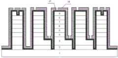
图24:本发明可直接连接在交流电上的LED芯片组结构示意图。Fig. 24: Schematic diagram of the structure of the LED chipset that can be directly connected to the alternating current according to the present invention.
附图标记说明:Explanation of reference signs:
1—衬底;2—缓冲层;3—N型层;4—N型分别限制层;5—有源区层;6—P型分别限制层;7—P型层;8—P型欧姆接触层;9—P型金属欧姆接触层;10—第一光刻胶层;11—第二光刻胶层;12—第三光刻胶层;121—刻蚀缺口;13—绝缘介质膜;14—第四光刻胶层;15—第五光刻胶层;16—金属合金层;160—输入电极金属层;161—输出电极金属层;162—PP结电极连接金属层;163—第一PN结电极连接金属层;164—第二PN结电极连接金属层;165—第三PN结电极连接金属层;17—P型金属欧姆接触层第一隔离缺口;18—P型金属欧姆接触层第二隔离缺口;R1—第一半导体电阻;R2—第二半导体电阻;L1—第一发光二极管;L2—第二发光二极管;L3—第三发光二极管。1—substrate; 2—buffer layer; 3—N-type layer; 4—N-type separate confinement layer; 5—active region layer; 6—P-type separate confinement layer; 7—P-type layer; 8—P-type ohm Contact layer; 9—P-type metal ohmic contact layer; 10—first photoresist layer; 11—second photoresist layer; 12—third photoresist layer; 121—etching gap; 13—insulating dielectric film ; 14—the fourth photoresist layer; 15—the fifth photoresist layer; 16—metal alloy layer; 160—input electrode metal layer; 161—output electrode metal layer; 162—PP junction electrode connection metal layer; 163— The first PN junction electrode is connected to the metal layer; 164—the second PN junction electrode is connected to the metal layer; 165—the third PN junction electrode is connected to the metal layer; 17—the first isolation gap of the P-type metal ohmic contact layer; 18—P-type metal ohmic The second isolation gap of the contact layer; R1—the first semiconductor resistor; R2—the second semiconductor resistor; L1—the first light emitting diode; L2—the second light emitting diode; L3—the third light emitting diode.
具体实施方式Detailed ways
下面结合图1至图24,对本发明做进一步说明:Below in conjunction with Fig. 1 to Fig. 24, the present invention will be further described:
如图1所示,普通发光二极管芯片从下至上依次为衬底1、缓冲层2、N型层3、N型分别限制层4、有源区层5、P型分别限制层6、P型层7以及P型欧姆接触层8。衬底1是载体,一般是蓝宝石、碳化硅或GaN等材料。缓冲层2是一个过度层,在此基础上生长高质量的N, P, 量子阱等其它材料。LED由pn结构成,缓冲层2、N型层3层、N型分别限制层4,P型分别限制层6以及P型层7是为了形成制作LED所需的P和N型材料。有源区层5是LED的发光区,光的颜色由有源区的结构决定。P型欧姆接触层8是材料生长的最后一层,这一层的载流子搀杂浓度较高,目的是为制作较小的欧姆接触电阻。As shown in Figure 1, the common light-emitting diode chips are
一种可直接连接在交流电上的LED芯片组制作方法如下:A manufacturing method of an LED chipset that can be directly connected to an alternating current is as follows:
1、在P型欧姆接触层8表面上方形成P型金属欧姆接触层9;1. Forming a P-type metal
2、将发光二极管芯片分割出多个独立单元,其中在发光二极管芯片两个端部的单元成为半导体电阻形成区;2. Dividing the light emitting diode chip into multiple independent units, wherein the units at both ends of the light emitting diode chip become semiconductor resistance forming regions;
3、将其余多个独立单元形成多个发光二极管形成区;3. Forming a plurality of light-emitting diode formation regions from the remaining independent units;
4、通过绝缘介质膜13将在发光二极管芯片上形成第一半导体电阻R1、第二半导体电阻R2和多个发光二极管L1、L2、L3;4. Form the first semiconductor resistor R1, the second semiconductor resistor R2 and a plurality of light-emitting diodes L1, L2, L3 on the light-emitting diode chip through the insulating
5、将第一半导体电阻R1、多个发光二极管以及第二半导体电阻R2的各个电极通过金属合金层16进行串联连接,即生成一枚集成电阻发光二极管芯片;5. Connect the electrodes of the first semiconductor resistor R1, a plurality of light-emitting diodes and the second semiconductor resistor R2 in series through the
6、使用步骤5中两枚集成电阻发光二极管芯片,将两枚集成电阻发光二极管芯片并联在交流电正负极,一枚集成电阻发光二极管芯片的第一半导体电阻R1和另一枚集成电阻发光二极管芯片的第二半导体电阻R2的连接端与交流电正极或负极直接连接,根据二极管正向导通原理两枚集成电阻发光二极管芯片在交流电作用下交替发光。6. Using the two integrated resistor LED chips in
具体详细步骤如下:The detailed steps are as follows:
如图2所示,在P型欧姆接触层8表面上方形成P型金属欧姆接触层9。通过蒸镀或溅射工艺,在P型欧姆接触层8表面形成一层或多层P型金属欧姆接触层9。P型金属欧姆接触层9不是由生长形成的,而是通过蒸镀或溅射等方法形成的,目的之一是制作器件的电极,目的之二是为了封装打线用。As shown in FIG. 2 , a P-type metal
如图3所示,在P型金属欧姆接触层9表面上方形成第一光刻胶层10。第一光刻胶层10涂布速度在2500-5000转/分,并对涂布温度控制90摄氏度-100摄氏度之间,在烘箱里或铁板表面烘烤,烘烤时间分别为30分钟和2分钟。As shown in FIG. 3 , a
如图4所示,去除部分第一光刻胶层10,保留的多块第一光刻胶层10用于制作半导体电阻形成区或发光二极管形成区。As shown in FIG. 4 , part of the
如图5所示,将暴露的P型材料、有源区以及部分N型材料进行去除。As shown in FIG. 5 , the exposed P-type material, active region and part of N-type material are removed.
如图6所示,去除剩下所有的第一光刻胶层10。As shown in FIG. 6, all remaining
如图7所示,对图6中所得到的发光二极管芯片表面上方形成第二光刻胶层11。第二光刻胶层11涂布速度在2500-5000转/分,并对涂布温度控制90摄氏度-100摄氏度之间,在烘箱里或铁板表面烘烤,烘烤时间分别为30分钟和2分钟。As shown in FIG. 7 , a
如图8所示,将半导体电阻形成区独立单元上方的第二光刻胶层11进行部分去除,形成缺口。As shown in FIG. 8 , the
如图9所示,对缺口下方的P型金属欧姆接触层9进行完整去除,形成P型金属欧姆接触层第一隔离缺口17和P型金属欧姆接触层第二隔离缺口18。As shown in FIG. 9 , the P-type metal
如图10所示,去除所有剩余的第二光刻胶层11。As shown in FIG. 10, all remaining
如图11所示,在图10中得到的发光二极管芯片表面上方形成第三光刻胶层12。第三光刻胶层12涂布速度在2500-5000转/分,并对涂布温度控制90摄氏度-100摄氏度之间,在烘箱里或铁板表面烘烤,烘烤时间分别为30分钟和2分钟。As shown in FIG. 11 , a
如图12所示,去除部分第三光刻胶层12,保留半导体电阻形成区最上方的第三光刻胶层12,保留多个发光二极管芯片形成区最上方和右侧的第三光刻胶层12,但发光二极管芯片形成区右侧的第三光刻胶层12与另外一个的发光二极管芯片形成区或第二半导体电阻形成区存在刻蚀缺口121。As shown in Figure 12, part of the
如图13所示,将未覆盖第三光刻胶层12的暴露部分进行刻蚀去除所有缓冲层2和N型层3;As shown in FIG. 13, the exposed part not covered with the
如图14所示,去除所有剩余的第三光刻胶层12。As shown in FIG. 14, all remaining
如图15所示,在图14中得到的发光二极管芯片表面上方形成绝缘介质膜13。绝缘介质膜13的厚度在150nm-450nm之间。As shown in FIG. 15 , an insulating
如图16所示,在绝缘介质膜13表面上方形成第四光刻胶层14。第四光刻胶层14涂布速度在2500-5000转/分,并对涂布温度控制90摄氏度-100摄氏度之间,在烘箱里或铁板表面烘烤,烘烤时间分别为30分钟和2分钟。As shown in FIG. 16 , a
如图17所示,去除部分第四光刻胶层14在两个半导体电阻的电极形成区和多个发光二级管的电极形成区上形成的多个缺口;As shown in FIG. 17 , removing part of the
如图18所示,将图17中多个缺口下方的绝缘介质膜13去除。As shown in FIG. 18 , the insulating
如图19所示,去除剩余所有的第四光刻胶层14。As shown in FIG. 19, all remaining
如图20所示,在图19中得到的发光二极管芯片表面上方形成第五光刻胶层15。第五光刻胶层15涂布速度在2500-5000转/分,并对涂布温度控制90摄氏度-100摄氏度之间,在烘箱里或铁板表面烘烤,烘烤时间分别为30分钟和2分钟。As shown in FIG. 20 , a
如图21所示,去除部分第五光刻胶层15,仅仅保留任何一个发光二级管P电极至N电极之间绝缘介质膜13上方的第五光刻胶层15、P型金属欧姆接触层第一隔离缺口17和P型金属欧姆接触层第二隔离缺口18中绝缘介质膜13上方的第五光刻胶层15、第一半导体电阻R1最左侧绝缘介质膜13上方的第五光刻胶以及第二半导体电阻R2最右侧绝缘介质膜13上方的第五光刻胶;As shown in FIG. 21, part of the
如图22所示,在图21中得到的发光二极管芯片表面上方形成金属合金层16。As shown in FIG. 22 , a
如图23所示,去除第五光刻胶层15及其上方的金属合金层16后,剩下的金属合金层16包括输入电极金属层160、输出电极金属层161、PP结电极连接金属层162以及多个PN结电极连接金属层163、164、165。As shown in FIG. 23, after removing the
如图24所示,使用两枚图23中制造出来的集成电阻发光二极管芯片,将两枚集成电阻发光二极管芯片并联在交流电正负极,一枚集成电阻发光二极管芯片的第一半导体电阻R1和另一枚集成电阻发光二极管芯片的第二半导体电阻R2的连接端与交流电正极或负极直接连接,根据二极管正向导通原理两枚集成电阻发光二极管芯片在交流电作用下交替发光。As shown in Figure 24, using two integrated resistance light emitting diode chips manufactured in Figure 23, the two integrated resistance light emitting diode chips are connected in parallel to the positive and negative poles of the alternating current, and the first semiconductor resistor R1 of one integrated resistance light emitting diode chip and The connection end of the second semiconductor resistor R2 of the other integrated resistance light-emitting diode chip is directly connected to the positive or negative pole of the alternating current, and the two integrated resistance light-emitting diode chips emit light alternately under the action of alternating current according to the principle of diode forward conduction.
上面结合附图对本发明进行了示例性的描述,显然本发明的实现并不受上述方式的限制,只要采用了本发明的方法构思和技术方案进行的各种改进,或未经改进将本发明的构思和技术方案直接应用于其它场合的,均在本发明的保护范围内。Above, the present invention has been exemplarily described in conjunction with the accompanying drawings. Obviously, the realization of the present invention is not limited by the above-mentioned manner, as long as various improvements of the method concept and technical solutions of the present invention are adopted, or the present invention is implemented without improvement. The ideas and technical schemes directly applied to other occasions are within the protection scope of the present invention.
Claims (3)
Translated fromChinesePriority Applications (1)
| Application Number | Priority Date | Filing Date | Title |
|---|---|---|---|
| CN 201110375793CN102412242B (en) | 2011-11-23 | 2011-11-23 | Light-emitting diode (LED) chipset capable of being connected to alternating current directly |
Applications Claiming Priority (1)
| Application Number | Priority Date | Filing Date | Title |
|---|---|---|---|
| CN 201110375793CN102412242B (en) | 2011-11-23 | 2011-11-23 | Light-emitting diode (LED) chipset capable of being connected to alternating current directly |
Publications (2)
| Publication Number | Publication Date |
|---|---|
| CN102412242A CN102412242A (en) | 2012-04-11 |
| CN102412242Btrue CN102412242B (en) | 2013-04-24 |
Family
ID=45914238
Family Applications (1)
| Application Number | Title | Priority Date | Filing Date |
|---|---|---|---|
| CN 201110375793Expired - Fee RelatedCN102412242B (en) | 2011-11-23 | 2011-11-23 | Light-emitting diode (LED) chipset capable of being connected to alternating current directly |
Country Status (1)
| Country | Link |
|---|---|
| CN (1) | CN102412242B (en) |
Families Citing this family (1)
| Publication number | Priority date | Publication date | Assignee | Title |
|---|---|---|---|---|
| CN103367386A (en)* | 2013-07-10 | 2013-10-23 | 中国科学院半导体研究所 | Alternating-current light-emitting diode (LED) |
Citations (5)
| Publication number | Priority date | Publication date | Assignee | Title |
|---|---|---|---|---|
| US5463280A (en)* | 1994-03-03 | 1995-10-31 | National Service Industries, Inc. | Light emitting diode retrofit lamp |
| US6410940B1 (en)* | 2000-06-15 | 2002-06-25 | Kansas State University Research Foundation | Micro-size LED and detector arrays for minidisplay, hyper-bright light emitting diodes, lighting, and UV detector and imaging sensor applications |
| JP3505374B2 (en)* | 1997-11-14 | 2004-03-08 | 三洋電機株式会社 | Light emitting components |
| CN1943276A (en)* | 2004-02-25 | 2007-04-04 | 迈克尔·米斯金 | AC light emitting diode and AC LED driving method and device |
| CN101072464A (en)* | 2006-10-06 | 2007-11-14 | 范朝阳 | Ac-dc light-emitting diode having integrated protection function |
- 2011
- 2011-11-23CNCN 201110375793patent/CN102412242B/ennot_activeExpired - Fee Related
Patent Citations (5)
| Publication number | Priority date | Publication date | Assignee | Title |
|---|---|---|---|---|
| US5463280A (en)* | 1994-03-03 | 1995-10-31 | National Service Industries, Inc. | Light emitting diode retrofit lamp |
| JP3505374B2 (en)* | 1997-11-14 | 2004-03-08 | 三洋電機株式会社 | Light emitting components |
| US6410940B1 (en)* | 2000-06-15 | 2002-06-25 | Kansas State University Research Foundation | Micro-size LED and detector arrays for minidisplay, hyper-bright light emitting diodes, lighting, and UV detector and imaging sensor applications |
| CN1943276A (en)* | 2004-02-25 | 2007-04-04 | 迈克尔·米斯金 | AC light emitting diode and AC LED driving method and device |
| CN101072464A (en)* | 2006-10-06 | 2007-11-14 | 范朝阳 | Ac-dc light-emitting diode having integrated protection function |
Also Published As
| Publication number | Publication date |
|---|---|
| CN102412242A (en) | 2012-04-11 |
Similar Documents
| Publication | Publication Date | Title |
|---|---|---|
| CN102637681B (en) | Vertical light-emitting device and manufacturing method thereof | |
| CN105552180B (en) | A kind of production method of novel high-pressure LED | |
| CN106981550B (en) | Easy-packaging easy-heat-dissipation inverted high-voltage LED chip | |
| CN102509731B (en) | Alternating current vertical light emitting element and manufacture method thereof | |
| WO2013044817A1 (en) | Inverted integrated led and production method thereof | |
| CN103151447B (en) | A kind of double-side diode structure and preparation method thereof | |
| CN103618042B (en) | A kind of semiconductor light-emitting diode chip | |
| WO2014048013A1 (en) | Preparation method for high-voltage led device integrated with pattern array | |
| CN102593304A (en) | A high-power LED lamp using ceramic heat dissipation | |
| WO2016011809A1 (en) | High-voltage light emitting diode chip and manufacturing method therefor | |
| CN102130241B (en) | Light emitting diode array structure and manufacturing method thereof | |
| CN101211957B (en) | Alternating current illuminating device and method for making the same | |
| CN102412242B (en) | Light-emitting diode (LED) chipset capable of being connected to alternating current directly | |
| JP2007188942A (en) | Light emitting diode device coupling rectifying circuit to sub-carrier and manufacturing method thereof | |
| CN102646694B (en) | High-voltage direct-current light-emitting diode and preparation method thereof | |
| CN202434517U (en) | Light emitting diode array | |
| CN102760746B (en) | A light-emitting diode chip with integrated resistor | |
| CN207116465U (en) | A kind of easily encapsulation easy heat radiation upside-down mounting high voltage LED chip | |
| CN103474446B (en) | Light emitting diode array structure and manufacturing method thereof | |
| CN103367386A (en) | Alternating-current light-emitting diode (LED) | |
| CN102403424B (en) | Method for manufacturing light-emitting diode chip of integrated resistor | |
| CN104269424B (en) | Light emitting diode chip for integrated resistor | |
| CN102412353B (en) | Manufacturing method for light-emitting diode (LED) chipset capable of being directly connected to alternating current | |
| TWI404230B (en) | Light emitting diodes with multi-layer stacking structure | |
| CN209183575U (en) | High power LED lamp panel |
Legal Events
| Date | Code | Title | Description |
|---|---|---|---|
| C06 | Publication | ||
| PB01 | Publication | ||
| C10 | Entry into substantive examination | ||
| SE01 | Entry into force of request for substantive examination | ||
| ASS | Succession or assignment of patent right | Owner name:NINGBO JIANGDONG KEHAI YUNTUO MACHINERY TECHNOLOGY Free format text:FORMER OWNER: YU GUOHONG Effective date:20130321 | |
| C41 | Transfer of patent application or patent right or utility model | ||
| COR | Change of bibliographic data | Free format text:CORRECT: ADDRESS; FROM: 322000 JINHUA, ZHEJIANG PROVINCE TO: 315000 NINGBO, ZHEJIANG PROVINCE | |
| TA01 | Transfer of patent application right | Effective date of registration:20130321 Address after:05, 315000, 001, 1088 (4-1) drive drive road, Jiangdong Road, Jiangdong, Zhejiang, Ningbo Applicant after:NINGBO JIANGDONG KEHAI YUNTUO MACHINERY TECHNOLOGY Co.,Ltd. Address before:3 floor 322000, E District, Yiwu International Trade City, Zhejiang, 8643 Applicant before:Yu Guohong | |
| C14 | Grant of patent or utility model | ||
| GR01 | Patent grant | ||
| ASS | Succession or assignment of patent right | Owner name:NANTONG SHIQIAO ELECTRONIC TECHBOLOGY CO., LTD. Free format text:FORMER OWNER: NINGBO JIANGDONG KEHAI YUNTUO MACHINERY TECHNOLOGY CO., LTD. Effective date:20131018 | |
| C41 | Transfer of patent application or patent right or utility model | ||
| COR | Change of bibliographic data | Free format text:CORRECT: ADDRESS; FROM: 315040 NINGBO, ZHEJIANG PROVINCE TO: 226000 NANTONG, JIANGSU PROVINCE | |
| TR01 | Transfer of patent right | Effective date of registration:20131018 Address after:226000 Jiangsu city of Nantong province Gangzha science and Technology Industrial Park District (tongNing Avenue West, Center for science and Technology Park Road North Block) Patentee after:Nantong stone bridge Electronic Technology Co.,Ltd. Address before:Jiangdong District 315040 Zhejiang city of Ningbo province was driving road No. 1088 building 001 room 05 (4-1) Patentee before:NINGBO JIANGDONG KEHAI YUNTUO MACHINERY TECHNOLOGY Co.,Ltd. | |
| TR01 | Transfer of patent right | Effective date of registration:20170622 Address after:226002 Jiangsu province Nantong Gangzha District Liu Road happy village happy village three groups Patentee after:Nantong happiness Industry Co.,Ltd. Address before:226000 Jiangsu city of Nantong province Gangzha science and Technology Industrial Park District (tongNing Avenue West, Center for science and Technology Park Road North Block) Patentee before:Nantong stone bridge Electronic Technology Co.,Ltd. | |
| TR01 | Transfer of patent right | ||
| TR01 | Transfer of patent right | Effective date of registration:20200430 Address after:226002 Building 1, No. 389, Tongliu Road, Gangzha District, Nantong City, Jiangsu Province Patentee after:JIANGSU XULI NEW ENERGY DEVELOPMENT CO.,LTD. Address before:226002 three groups of happy village, happy village, Liu Road, Gangzha District, Nantong, Jiangsu Patentee before:Nantong happiness Industry Co.,Ltd. | |
| TR01 | Transfer of patent right | ||
| TR01 | Transfer of patent right | Effective date of registration:20201125 Address after:215400 Taicang Economic Development Zone, Jiangsu, Beijing West Road, No. 6, No. Patentee after:SUZHOU ZHENRUICHANG MATERIAL TECHNOLOGY Co.,Ltd. Address before:226002 Building 1, No. 389, Tongliu Road, Gangzha District, Nantong City, Jiangsu Province Patentee before:JIANGSU XULI NEW ENERGY DEVELOPMENT Co.,Ltd. | |
| TR01 | Transfer of patent right | ||
| CF01 | Termination of patent right due to non-payment of annual fee | ||
| CF01 | Termination of patent right due to non-payment of annual fee | Granted publication date:20130424 |