CN102403363A - Double-layered oxide thin film transistor and preparation method thereof - Google Patents
Double-layered oxide thin film transistor and preparation method thereofDownload PDFInfo
- Publication number
- CN102403363A CN102403363ACN2011103302122ACN201110330212ACN102403363ACN 102403363 ACN102403363 ACN 102403363ACN 2011103302122 ACN2011103302122 ACN 2011103302122ACN 201110330212 ACN201110330212 ACN 201110330212ACN 102403363 ACN102403363 ACN 102403363A
- Authority
- CN
- China
- Prior art keywords
- coating
- layer
- oxide skin
- oxide
- preparation
- Prior art date
- Legal status (The legal status is an assumption and is not a legal conclusion. Google has not performed a legal analysis and makes no representation as to the accuracy of the status listed.)
- Pending
Links
- 239000010409thin filmSubstances0.000titleclaimsabstractdescription50
- 238000002360preparation methodMethods0.000titleclaimsabstractdescription37
- XKRFYHLGVUSROY-UHFFFAOYSA-NArgonChemical compound[Ar]XKRFYHLGVUSROY-UHFFFAOYSA-N0.000claimsabstractdescription36
- 239000000758substrateSubstances0.000claimsabstractdescription24
- 229910052786argonInorganic materials0.000claimsabstractdescription18
- 238000000034methodMethods0.000claimsabstractdescription18
- QVGXLLKOCUKJST-UHFFFAOYSA-Natomic oxygenChemical compound[O]QVGXLLKOCUKJST-UHFFFAOYSA-N0.000claimsabstractdescription12
- 239000001301oxygenSubstances0.000claimsabstractdescription12
- 229910052760oxygenInorganic materials0.000claimsabstractdescription12
- 239000000463materialSubstances0.000claimsdescription43
- PXHVJJICTQNCMI-UHFFFAOYSA-NNickelChemical compound[Ni]PXHVJJICTQNCMI-UHFFFAOYSA-N0.000claimsdescription19
- 229910052782aluminiumInorganic materials0.000claimsdescription19
- XAGFODPZIPBFFR-UHFFFAOYSA-NaluminiumChemical compound[Al]XAGFODPZIPBFFR-UHFFFAOYSA-N0.000claimsdescription18
- 229910000838Al alloyInorganic materials0.000claimsdescription15
- VYPSYNLAJGMNEJ-UHFFFAOYSA-NSilicium dioxideChemical compoundO=[Si]=OVYPSYNLAJGMNEJ-UHFFFAOYSA-N0.000claimsdescription12
- 239000007789gasSubstances0.000claimsdescription12
- 239000010408filmSubstances0.000claimsdescription11
- 229910052759nickelInorganic materials0.000claimsdescription9
- 229910052715tantalumInorganic materials0.000claimsdescription9
- GUVRBAGPIYLISA-UHFFFAOYSA-Ntantalum atomChemical compound[Ta]GUVRBAGPIYLISA-UHFFFAOYSA-N0.000claimsdescription9
- 229910052725zincInorganic materials0.000claimsdescription9
- 239000011701zincSubstances0.000claimsdescription9
- HCHKCACWOHOZIP-UHFFFAOYSA-NZincChemical compound[Zn]HCHKCACWOHOZIP-UHFFFAOYSA-N0.000claimsdescription8
- 238000005229chemical vapour depositionMethods0.000claimsdescription8
- ZOKXTWBITQBERF-UHFFFAOYSA-NMolybdenumChemical compound[Mo]ZOKXTWBITQBERF-UHFFFAOYSA-N0.000claimsdescription7
- 239000011651chromiumSubstances0.000claimsdescription7
- 239000010949copperSubstances0.000claimsdescription7
- 239000010931goldSubstances0.000claimsdescription7
- 229910052750molybdenumInorganic materials0.000claimsdescription7
- 239000011733molybdenumSubstances0.000claimsdescription7
- 239000010955niobiumSubstances0.000claimsdescription7
- 230000003647oxidationEffects0.000claimsdescription7
- 238000007254oxidation reactionMethods0.000claimsdescription7
- 239000010936titaniumSubstances0.000claimsdescription7
- VYZAMTAEIAYCRO-UHFFFAOYSA-NChromiumChemical compound[Cr]VYZAMTAEIAYCRO-UHFFFAOYSA-N0.000claimsdescription6
- RYGMFSIKBFXOCR-UHFFFAOYSA-NCopperChemical compound[Cu]RYGMFSIKBFXOCR-UHFFFAOYSA-N0.000claimsdescription6
- 229910052779NeodymiumInorganic materials0.000claimsdescription6
- BQCADISMDOOEFD-UHFFFAOYSA-NSilverChemical compound[Ag]BQCADISMDOOEFD-UHFFFAOYSA-N0.000claimsdescription6
- RTAQQCXQSZGOHL-UHFFFAOYSA-NTitaniumChemical compound[Ti]RTAQQCXQSZGOHL-UHFFFAOYSA-N0.000claimsdescription6
- 229910052804chromiumInorganic materials0.000claimsdescription6
- 229910052802copperInorganic materials0.000claimsdescription6
- PCHJSUWPFVWCPO-UHFFFAOYSA-NgoldChemical compound[Au]PCHJSUWPFVWCPO-UHFFFAOYSA-N0.000claimsdescription6
- 229910052737goldInorganic materials0.000claimsdescription6
- 229910052738indiumInorganic materials0.000claimsdescription6
- QEFYFXOXNSNQGX-UHFFFAOYSA-Nneodymium atomChemical compound[Nd]QEFYFXOXNSNQGX-UHFFFAOYSA-N0.000claimsdescription6
- 229910052758niobiumInorganic materials0.000claimsdescription6
- GUCVJGMIXFAOAE-UHFFFAOYSA-Nniobium atomChemical compound[Nb]GUCVJGMIXFAOAE-UHFFFAOYSA-N0.000claimsdescription6
- 239000000377silicon dioxideSubstances0.000claimsdescription6
- 235000012239silicon dioxideNutrition0.000claimsdescription6
- 229910052709silverInorganic materials0.000claimsdescription6
- 239000004332silverSubstances0.000claimsdescription6
- 239000000126substanceSubstances0.000claimsdescription6
- 229910052719titaniumInorganic materials0.000claimsdescription6
- WFKWXMTUELFFGS-UHFFFAOYSA-NtungstenChemical compound[W]WFKWXMTUELFFGS-UHFFFAOYSA-N0.000claimsdescription6
- 229910052721tungstenInorganic materials0.000claimsdescription6
- 239000010937tungstenSubstances0.000claimsdescription6
- 229910052581Si3N4Inorganic materials0.000claimsdescription5
- APFVFJFRJDLVQX-UHFFFAOYSA-Nindium atomChemical compound[In]APFVFJFRJDLVQX-UHFFFAOYSA-N0.000claimsdescription5
- HQVNEWCFYHHQES-UHFFFAOYSA-Nsilicon nitrideChemical compoundN12[Si]34N5[Si]62N3[Si]51N64HQVNEWCFYHHQES-UHFFFAOYSA-N0.000claimsdescription5
- ATJFFYVFTNAWJD-UHFFFAOYSA-NTinChemical compound[Sn]ATJFFYVFTNAWJD-UHFFFAOYSA-N0.000claimsdescription3
- 229910052718tinInorganic materials0.000claimsdescription3
- 239000012780transparent materialSubstances0.000claimsdescription3
- 238000007738vacuum evaporationMethods0.000claimsdescription3
- 239000011248coating agentSubstances0.000claims21
- 238000000576coating methodMethods0.000claims21
- 230000004888barrier functionEffects0.000claims10
- 238000001259photo etchingMethods0.000claims4
- MRNHPUHPBOKKQT-UHFFFAOYSA-Nindium;tin;hydrateChemical compoundO.[In].[Sn]MRNHPUHPBOKKQT-UHFFFAOYSA-N0.000claims2
- 239000004411aluminiumSubstances0.000claims1
- 238000004544sputter depositionMethods0.000abstractdescription25
- XLOMVQKBTHCTTD-UHFFFAOYSA-NZinc monoxideChemical compound[Zn]=OXLOMVQKBTHCTTD-UHFFFAOYSA-N0.000description15
- 238000000206photolithographyMethods0.000description13
- 239000011521glassSubstances0.000description12
- 238000012546transferMethods0.000description8
- 239000011787zinc oxideSubstances0.000description7
- 229910018072Al 2 O 3Inorganic materials0.000description6
- MYMOFIZGZYHOMD-UHFFFAOYSA-NDioxygenChemical compoundO=OMYMOFIZGZYHOMD-UHFFFAOYSA-N0.000description6
- 229910001882dioxygenInorganic materials0.000description6
- 239000004065semiconductorSubstances0.000description6
- 239000013077target materialSubstances0.000description6
- 229910044991metal oxideInorganic materials0.000description5
- 150000004706metal oxidesChemical class0.000description5
- AMGQUBHHOARCQH-UHFFFAOYSA-Nindium;oxotinChemical compound[In].[Sn]=OAMGQUBHHOARCQH-UHFFFAOYSA-N0.000description4
- 238000012360testing methodMethods0.000description4
- LYCAIKOWRPUZTN-UHFFFAOYSA-NEthylene glycolChemical compoundOCCOLYCAIKOWRPUZTN-UHFFFAOYSA-N0.000description3
- 229910045601alloyInorganic materials0.000description3
- 239000000956alloySubstances0.000description3
- 229910021417amorphous siliconInorganic materials0.000description3
- 239000000969carrierSubstances0.000description3
- GQPLMRYTRLFLPF-UHFFFAOYSA-NNitrous OxideChemical compound[O-][N+]#NGQPLMRYTRLFLPF-UHFFFAOYSA-N0.000description2
- 229910004298SiO 2Inorganic materials0.000description2
- 239000008151electrolyte solutionSubstances0.000description2
- 239000000203mixtureSubstances0.000description2
- 238000000059patterningMethods0.000description2
- 229910021420polycrystalline siliconInorganic materials0.000description2
- IJGRMHOSHXDMSA-UHFFFAOYSA-NAtomic nitrogenChemical compoundN#NIJGRMHOSHXDMSA-UHFFFAOYSA-N0.000description1
- GYHNNYVSQQEPJS-UHFFFAOYSA-NGalliumChemical compound[Ga]GYHNNYVSQQEPJS-UHFFFAOYSA-N0.000description1
- BLRPTPMANUNPDV-UHFFFAOYSA-NSilaneChemical compound[SiH4]BLRPTPMANUNPDV-UHFFFAOYSA-N0.000description1
- XUIMIQQOPSSXEZ-UHFFFAOYSA-NSiliconChemical compound[Si]XUIMIQQOPSSXEZ-UHFFFAOYSA-N0.000description1
- 229910007717ZnSnOInorganic materials0.000description1
- NGPGDYLVALNKEG-UHFFFAOYSA-Nazanium;azane;2,3,4-trihydroxy-4-oxobutanoateChemical compound[NH4+].[NH4+].[O-]C(=O)C(O)C(O)C([O-])=ONGPGDYLVALNKEG-UHFFFAOYSA-N0.000description1
- 230000009286beneficial effectEffects0.000description1
- 230000005540biological transmissionEffects0.000description1
- 239000004020conductorSubstances0.000description1
- 230000007423decreaseEffects0.000description1
- 230000007547defectEffects0.000description1
- 230000007812deficiencyEffects0.000description1
- 238000011161developmentMethods0.000description1
- AJNVQOSZGJRYEI-UHFFFAOYSA-Ndigallium;oxygen(2-)Chemical compound[O-2].[O-2].[O-2].[Ga+3].[Ga+3]AJNVQOSZGJRYEI-UHFFFAOYSA-N0.000description1
- 229910001873dinitrogenInorganic materials0.000description1
- 238000005516engineering processMethods0.000description1
- 229910052733galliumInorganic materials0.000description1
- 229910001195gallium oxideInorganic materials0.000description1
- 239000004973liquid crystal related substanceSubstances0.000description1
- 230000000873masking effectEffects0.000description1
- 230000008018meltingEffects0.000description1
- 238000002844meltingMethods0.000description1
- 235000013842nitrous oxideNutrition0.000description1
- KYKLWYKWCAYAJY-UHFFFAOYSA-Noxotin;zincChemical compound[Zn].[Sn]=OKYKLWYKWCAYAJY-UHFFFAOYSA-N0.000description1
- 229920005591polysiliconPolymers0.000description1
- 238000011160researchMethods0.000description1
- 230000035945sensitivityEffects0.000description1
- 229910000077silaneInorganic materials0.000description1
- 229910052710siliconInorganic materials0.000description1
- 239000010703siliconSubstances0.000description1
- 239000002210silicon-based materialSubstances0.000description1
- 239000000243solutionSubstances0.000description1
- 239000010935stainless steelSubstances0.000description1
- 229910001220stainless steelInorganic materials0.000description1
- JBQYATWDVHIOAR-UHFFFAOYSA-NtellanylidenegermaniumChemical compound[Te]=[Ge]JBQYATWDVHIOAR-UHFFFAOYSA-N0.000description1
- 230000007704transitionEffects0.000description1
Images


Landscapes
- Thin Film Transistor (AREA)
Abstract
Translated fromChinese
Description
Translated fromChinese技术领域technical field
本发明涉及一种薄膜晶体管,特别是涉及一种金属氧化物薄膜晶体管及其制备方法,该薄膜晶体管主要用于有机发光显示、液晶显示以及电子纸的有源驱动,也可以用于集成电路。The invention relates to a thin film transistor, in particular to a metal oxide thin film transistor and a preparation method thereof. The thin film transistor is mainly used for active driving of organic light emitting display, liquid crystal display and electronic paper, and can also be used for integrated circuits.
背景技术Background technique
近年来,基于金属氧化物的薄膜晶体管因为其迁移率高、透光性好、薄膜结构稳定、制备温度低以及成本低等优点受到越来越多的重视。金属氧化物薄膜晶体管的发展主要目标是用于平板显示、柔性电子器件、透明电子器件以及传感器等方面。在平板显示方面,目前主要使用氢化非晶硅(a-Si:H)或多晶硅等材料的薄膜晶体管,然而氢化非晶硅材料的局限性主要表现在对光敏感、电子迁移率低(<1cm2/Vs)以及电学参数稳定性差等方面,而多晶硅薄膜的局限性主要体现在电学性质均匀性差、制备温度高以及成本高等方面。In recent years, thin film transistors based on metal oxides have attracted more and more attention because of their advantages such as high mobility, good light transmission, stable film structure, low preparation temperature and low cost. The main goal of the development of metal oxide thin film transistors is to be used in flat panel displays, flexible electronic devices, transparent electronic devices, and sensors. In terms of flat panel display, thin-film transistors made of materials such as hydrogenated amorphous silicon (a-Si:H) or polycrystalline silicon are currently mainly used. However, the limitations of hydrogenated amorphous silicon materials are mainly reflected in their sensitivity to light and low electron mobility (<1cm2 /Vs) and poor stability of electrical parameters, while the limitations of polysilicon thin films are mainly reflected in the poor uniformity of electrical properties, high preparation temperature and high cost.
氧化物半导体材料主要包括氧化锌(ZnO)、氧化铟镓(InGaO)、氧化锌锡(ZnSnO)、氧化铟镓锌(InGaZnO)等。基于这些金属氧化物的薄膜晶体管电子迁移率较高(1~100cm2/Vs)、制备温度低(<400℃,远远低于玻璃的熔点)、成本低(只需要普通的溅射工艺即可完成)以及持续工作稳定性好。正因为如此,基于氧化物的薄膜晶体管在平板显示领域尤其是有机发光显示(OLED)领域有替代传统的硅材料工艺薄膜晶体管的趋势,受到学术界和业界的关注和广泛研究。Oxide semiconductor materials mainly include zinc oxide (ZnO), indium gallium oxide (InGaO), zinc tin oxide (ZnSnO), indium gallium zinc oxide (InGaZnO), etc. Thin film transistors based on these metal oxides have high electron mobility (1~100cm2 /Vs), low preparation temperature (<400°C, far below the melting point of glass), and low cost (only ordinary sputtering process is required. can be completed) and continuous work stability is good. Because of this, oxide-based thin-film transistors tend to replace traditional silicon-based thin-film transistors in the field of flat-panel displays, especially in the field of organic light-emitting displays (OLEDs), and have attracted attention and extensive research from academia and the industry.
通常,基于氧化物的薄膜晶体管都是只含有单层氧化物层,即只有一层氧化物半导体层,由于氧化物半导体的本征载流子浓度较大,这种器件的阈值电压为负值,关态电流较大,造成电流开关比较小。Generally, oxide-based thin film transistors contain only a single oxide layer, that is, only one oxide semiconductor layer. Due to the high intrinsic carrier concentration of oxide semiconductors, the threshold voltage of such devices is negative. , the off-state current is larger, resulting in a smaller current switch.
发明内容Contents of the invention
本发明的目的在于克服现有技术中存在的缺点与不足,提供一种双层氧化物薄膜晶体管及其制备方法,本发明提出一种既能够抑制过剩的本征载流子、提高阈值电压、降低关态电流、提高电流开关比,同时又能够改善绝缘层和氧化物半导体层的接触,提高稳定性的新型双层氧化物薄膜晶体管及其制备方法。The purpose of the present invention is to overcome the shortcomings and deficiencies in the prior art, and to provide a double-layer oxide thin film transistor and its preparation method. The present invention proposes a method that can suppress excess intrinsic carriers, increase threshold voltage, A novel double-layer oxide thin film transistor and a preparation method thereof can reduce the off-state current, increase the current switching ratio, improve the contact between the insulating layer and the oxide semiconductor layer, and improve the stability.
本发明的目的通过如下技术方案实现:The purpose of the present invention is achieved through the following technical solutions:
一种双层氧化物薄膜晶体管,包括基板、栅极、绝缘层、第一层氧化物层、第二层氧化物层、源极和漏极;从上到下依次是第二层氧化物层、第一层氧化物层、绝缘层、栅极、基板,绝缘层覆盖在栅极之上,源极和漏极分别覆盖在第二层氧化物层的两端并且相互间隔,所述的第一层氧化物层和第二层氧化物使用同一靶材,所述的靶材的材料的化学式为(Al2O3)x(In2O3)y(ZnO)1-x-y 其中0<x≤0.2、0.3≤y≤0.8。A double-layer oxide thin film transistor, including a substrate, a gate, an insulating layer, a first oxide layer, a second oxide layer, a source and a drain; from top to bottom is the second oxide layer , a first oxide layer, an insulating layer, a gate, and a substrate, the insulating layer covers the gate, the source and the drain cover the two ends of the second oxide layer and are spaced from each other, the first The first oxide layer and the second oxide layer use the same target, and the chemical formula of the target material is (Al2 O3 )x (In2 O3 )y (ZnO)1-xy where 0<x ≤0.2, 0.3≤y≤0.8.
所述第一层氧化物层的厚度为2~10nm、载流子浓度小于1016cm-3,第二层氧化物层的厚度为20~100nm、载流子浓度大于1017cm-3。The first oxide layer has a thickness of 2-10 nm and a carrier concentration of less than 1016 cm-3 , and the second oxide layer has a thickness of 20-100 nm and a carrier concentration of greater than 1017 cm-3 .
所述的靶材的材料进一步包括钽、钕、镍、锡中的一种以上元素,这些元素的原子数与铝、锌、铟三种元素的原子数之和的比例为0~0.05。所述的栅极的材料为铝或铝合金时,则所述的绝缘层为铝或铝合金的氧化物;所述的栅极的材料为钼、铬、金、银、铜、镍、锌、钛、铌、钽、钨或氧化铟锡时,则所述绝缘层材料为二氧化硅或氮化硅。The material of the target further includes more than one element among tantalum, neodymium, nickel, and tin, and the ratio of the atomic numbers of these elements to the sum of the atomic numbers of the three elements of aluminum, zinc, and indium is 0-0.05. When the material of the grid is aluminum or aluminum alloy, the insulating layer is an oxide of aluminum or aluminum alloy; the material of the grid is molybdenum, chromium, gold, silver, copper, nickel, zinc , titanium, niobium, tantalum, tungsten or indium tin oxide, the insulating layer material is silicon dioxide or silicon nitride.
所述的基板为透明材料,厚度为0.2~1mm。The substrate is a transparent material with a thickness of 0.2-1 mm.
所述的双层氧化物薄膜晶体管的制备方法,其特征在于包括如下步骤:The preparation method of the described double-layer oxide thin film transistor is characterized in that it comprises the following steps:
(1)栅极的制备(1) Preparation of gate
在基板上采用溅射的方法制备一层厚度为100~500nm的栅极材料的薄膜,并采用掩模或光刻的方法图形化得到栅极;Prepare a thin film of gate material with a thickness of 100-500nm on the substrate by sputtering, and pattern the gate by using a mask or photolithography;
(2)绝缘层的制备(2) Preparation of insulating layer
所述绝缘层采用阳极氧化或化学气相沉积的方法制备得到厚度为100~1000nm的绝缘层材料的薄膜,并采用掩模或光刻的方法图形化得到绝缘层;若所述的栅极的材料为铝或铝合金,则所述的绝缘层采用阳极氧化的方法制备得到铝或铝合金的氧化物;若所述的栅极的材料为钼、铬、金、银、铜、镍、锌、钛、铌、钽、钨或氧化铟锡时,则所述的绝缘层采用化学气相沉积的方法制备得到二氧化硅或氮化硅;The insulating layer is prepared by anodic oxidation or chemical vapor deposition to obtain a thin film of insulating layer material with a thickness of 100-1000 nm, and the insulating layer is patterned by using a mask or photolithography; if the material of the gate is aluminum or aluminum alloy, then the insulating layer is prepared by anodic oxidation method to obtain the oxide of aluminum or aluminum alloy; if the material of the grid is molybdenum, chromium, gold, silver, copper, nickel, zinc, When titanium, niobium, tantalum, tungsten or indium tin oxide are used, the insulating layer is prepared by chemical vapor deposition to obtain silicon dioxide or silicon nitride;
(3)第一层氧化物层、第二层氧化物层的制备(3) Preparation of the first oxide layer and the second oxide layer
在绝缘层上面通过连续两次溅射的方法制备得到厚度为2~10nm的第一层氧化物层、厚度为20~100nm的第二层氧化物层,所述的第一层氧化物层和第二层氧化物层采用掩模或光刻的方法同时图形化,在制备过程中使用同一个靶材,并通过控制氧气与氩气的流量来控制氧化物层中的载流子浓度; On the insulating layer, a first oxide layer with a thickness of 2-10 nm and a second oxide layer with a thickness of 20-100 nm are prepared by two consecutive sputtering methods, the first oxide layer and The second oxide layer is simultaneously patterned by mask or photolithography, using the same target in the preparation process, and controlling the carrier concentration in the oxide layer by controlling the flow of oxygen and argon;
(4)漏极和源极的制备(4) Preparation of drain and source electrodes
在所述的第二层氧化物层的两端采用真空蒸镀或溅射的方法制备得到厚度为100~1000nm的源极和漏极的薄膜材料,并采用掩模或光刻的方法图形化得到漏极和源极。Prepare source and drain thin film materials with a thickness of 100-1000 nm at both ends of the second oxide layer by vacuum evaporation or sputtering, and pattern them by mask or photolithography Get the drain and source.
所述步骤(3)中在制备第一层氧化物层时,氧气与氩气的流量比大于0.3,在制备第二层氧化物层时,氧气与氩气的流量比小于 0.2。In the step (3), when preparing the first oxide layer, the flow ratio of oxygen to argon is greater than 0.3, and when preparing the second oxide layer, the flow ratio of oxygen to argon is less than 0.2.
本发明提出的双层氧化物薄膜晶体管及其制备方法的最重要的特征是具有双层氧化物层的的结构。其中第一层氧化物层的载流子浓度较低(小于1016cm-3),主要起过渡作用;第二层氧化物层的载流子浓度较高(大于1017cm-3),主要起半导体的作用。由于第一层氧化物层的载流子浓度较低,所以器件较容易关断,并且当器件关断时,流经第一层氧化物层及其上下界面的电流也能得到减小,从而能降低关态电流,提高电子迁移率,提高电流开关比;当器件导通时,由于载流子浓度很高,而第一层氧化物层很薄,远远无法容纳高浓度的载流子,所以载流子仍然主要聚集在第二层氧化物层上,这时由于第一层氧化物和第二层氧化物层的材料成份相似,所以它们之间的界面的缺陷较少,能提高器件的稳定性。The most important feature of the double-layer oxide thin film transistor and its preparation method proposed by the present invention is the structure with double-layer oxide layers. Among them, the carrier concentration of the first oxide layer is low (less than 1016 cm-3 ), which mainly plays a transition role; the carrier concentration of the second oxide layer is higher (greater than 1017 cm-3 ), It mainly functions as a semiconductor. Due to the lower carrier concentration of the first oxide layer, the device is easier to turn off, and when the device is turned off, the current flowing through the first oxide layer and its upper and lower interfaces can also be reduced, thereby It can reduce the off-state current, increase the electron mobility, and increase the current switching ratio; when the device is turned on, because the carrier concentration is very high, and the first oxide layer is very thin, it is far from being able to accommodate the high concentration of carriers , so the carriers are still mainly gathered on the second oxide layer. At this time, since the material composition of the first oxide layer and the second oxide layer are similar, there are fewer defects in the interface between them, which can improve device stability.
相对于现有技术,本发明具有如下优点和有益特征: With respect to prior art, the present invention has following advantage and beneficial feature:
(1)本发明的双层氧化物薄膜晶体管包括双层氧化物层的的结构,能有效降低关态电流,提高电流的开关比,提高器件的电学稳定性,这种不同含氧量的双层结构不同于传统的半导体晶体管只有含氧量均一的一层金属氧化物层;(1) The double-layer oxide thin film transistor of the present invention includes a double-layer oxide layer structure, which can effectively reduce the off-state current, increase the current switching ratio, and improve the electrical stability of the device. The layer structure is different from the traditional semiconductor transistor with only one metal oxide layer with uniform oxygen content;
(2)本发明的双层氧化物薄膜晶体管的第一层氧化物层和第二层氧化物层是用同一个靶材进行连续两次溅射获得,两次溅射之间无需移动基片位置,并且这两层薄膜是一起图形化的,因此,既能改善性能,又不会增加工艺难度。(2) The first oxide layer and the second oxide layer of the double-layer oxide thin film transistor of the present invention are obtained by using the same target for two consecutive sputterings, without moving the substrate between the two sputterings position, and the two layers of film are patterned together, so performance can be improved without increasing process difficulty.
附图说明Description of drawings
图1 是本发明的双层氧化物薄膜晶体管结构示意图;Fig. 1 is the structural representation of double-layer oxide thin film transistor of the present invention;
图2是本发明的双层氧化物薄膜晶体管的沟道的俯视图;Fig. 2 is the top view of the channel of the double-layer oxide thin film transistor of the present invention;
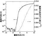
图3是实施例1中的转移特性曲线,即在源漏电极之间施加5V电压时,输出电流与栅极电压之间的关系曲线;Fig. 3 is the transfer characteristic curve in embodiment 1, namely when 5V voltage is applied between the source and drain electrodes, the relationship curve between the output current and the gate voltage;
图4是实施例2中的转移特性曲线,即在源漏电极之间施加5V电压时,输出电流与栅极电压之间的关系曲线;Fig. 4 is the transfer characteristic curve in embodiment 2, namely when 5V voltage is applied between the source and drain electrodes, the relationship curve between the output current and the gate voltage;
图5是实施例3中的转移特性曲线,即在源漏电极之间施加5V电压时,输出电流与栅极电压之间的关系曲线;Fig. 5 is the transfer characteristic curve in embodiment 3, namely when 5V voltage is applied between the source and drain electrodes, the relationship curve between the output current and the gate voltage;
图6是实施例4中的转移特性曲线,即在源漏电极之间施加5V电压时,输出电流与栅极电压之间的关系曲线。FIG. 6 is the transfer characteristic curve in Embodiment 4, that is, the relationship curve between the output current and the gate voltage when a voltage of 5V is applied between the source and drain electrodes.
具体实施方式Detailed ways
下面结合附图和实施例对本发明做进一步的说明,但本发明要求保护的范围并不局限于实施例表述的范围。The present invention will be further described below in conjunction with the accompanying drawings and examples, but the protection scope of the present invention is not limited to the range expressed in the examples.
图1显示了根据实施方式中所述的双层氧化物薄膜晶体管的结构,其包括:包括基板10、栅极11、绝缘层12、第一层氧化物层13、第二层氧化物层14、源极15a和漏极15b;从上到下依次是第二层氧化物层14、第一层氧化物层13、绝缘层12、栅极11、基板10,绝缘层12覆盖在栅极11之上,源极15a和漏极15b分别覆盖在第二层氧化物层14的两端并且相互间隔;FIG. 1 shows the structure of a double-layer oxide thin film transistor according to an embodiment, which includes: a
如图2所示:源极15a和漏极15b的间隔左右两端的距离即为沟道长度(L),源漏电极的前后端的长度即为沟道宽度(W)。As shown in FIG. 2 , the distance between the
基板10的材料为透明材料,厚度为0.2~1mm。The material of the
首先在玻璃基板上通过溅射的方法制备一层厚度为100~500nm的栅极材料的薄膜,通过掩模或光刻的方法图形化,得到栅极11。First, a thin film of gate material with a thickness of 100-500 nm is prepared on a glass substrate by sputtering, and patterned by a mask or photolithography to obtain the gate 11 .
所述的栅极的材料为铝或铝合金时,则所述的绝缘层为通过阳极氧化的方法制备得到铝或铝合金的氧化物;所述的栅极的材料为钼、铬、金、银、铜、镍、锌、钛、铌、钽、钨或氧化铟锡时,则所述绝缘层材料为通过化学气相沉积的方法制备得到二氧化硅或氮化硅。When the material of the grid is aluminum or aluminum alloy, the insulating layer is an oxide of aluminum or aluminum alloy prepared by anodic oxidation; the material of the grid is molybdenum, chromium, gold, In the case of silver, copper, nickel, zinc, titanium, niobium, tantalum, tungsten or indium tin oxide, the insulating layer material is silicon dioxide or silicon nitride prepared by chemical vapor deposition.
若栅极11的材料为铝或铝合金,则绝缘层12通过阳极氧化的方法制备。If the material of the gate 11 is aluminum or aluminum alloy, the
第一层氧化物层13和第二层氧化物层14依次通过对同一靶材经过两次溅射制备,第一层氧化物层13的厚度为2~10nm,第二层氧化物层14的厚度为20~100nm;第一层氧化物层13的载流子浓度小于1016cm-3,第二层氧化物层14的载流子浓度大于1017cm-3。第一层氧化物层13和第二层氧化物层14的载流子浓度通过溅射过程中的氧气和氩气的流量控制,在溅射制备第一层氧化物层13时,氧气与氩气的比例大于0.3,在溅射制备第二层氧化物层14时,氧气与氩气的流量比小于0.2。第一层氧化物层13和第二层氧化物层14通过掩模或光刻的方法一起图形化,得到完全重叠的图形,如图1B所示。The first layer of
第一层氧化物层13和第二层氧化物层14的制备使用同一靶材,靶材的材料的化学式为(Al2O3)x(In2O3)y(ZnO)1-x-y 其中0<x≤0.2、0.3≤y≤0.8。The same target is used for the preparation of the
所述的靶材的材料进一步包括钽、钕、镍、锡中的一种以上元素,这些元素的原子数与铝、锌、铟三种元素的原子数之和的比例为0~0.05。第二层氧化物层14两端采用真空蒸镀或溅射的方法制备所述的源极15a和漏极15b,厚度为100~1000nm,采用光刻或者掩模技术图形化。源极15a和漏极15b的材料可以是铝(Al)、钼(Mo)、铬(Cr)、金(Au)、银(Ag)、铜(Cu)、镍(Ni)、锌(Zn)、钛(Ti)、铌(Nb)、钽(Ta)、钨(W)或氧化铟锡(ITO)等导电材料。The material of the target further includes more than one element among tantalum, neodymium, nickel, and tin, and the ratio of the atomic numbers of these elements to the sum of the atomic numbers of the three elements of aluminum, zinc, and indium is 0-0.05. Both ends of the
下面通过4个具体实施例对本发明做进一步的详细描述。The present invention will be further described in detail through 4 specific examples below.
实施例1Example 1
本实施例利用铝合金(铝和钕的合金)作为栅极11材料。玻璃基板10的材料为无碱玻璃,厚度为0.4mm。In this embodiment, aluminum alloy (alloy of aluminum and neodymium) is used as the material of the grid 11 . The material of the
首先在玻璃基板10上通过溅射的方法制备一层厚度为300nm的铝合金薄膜,溅射本底真空度优于1×10⁻³Pa,氩气流量为60SCCM,功率为10W/cm2,厚度为300nm,通过光刻的方法图形化得到栅极11。 First, a layer of aluminum alloy thin film with a thickness of 300nm is prepared on the
绝缘层12为通过阳极氧化制备,阳极氧化中使用的电解质溶液可以是酒石酸铵和乙二醇的混合液,将制备好栅极11的基片和不锈钢板放入电解质溶液中分别作为阳极和阴极,先在阳极和阴极之间加恒定的电流0.1mA /cm2,阳极和阴极之间的电压将随时间线性升高,当电压达到100V,恒定100V,直至阳极和阴极之间的电流减小至约为0.001 mA/cm2时,将基片取出用氮气吹干再清洗,测得氧化膜厚度为140nm。The insulating
第一层氧化物层13和第二层氧化物层14的制备使用同一靶材,靶材的材料的化学式为(Al2O3)0.05(In2O3)0.3(ZnO)0.55,即x=0.05、y=0.3,此外,靶材中进一步包含Nd元素,Nd的原子数与Al、Zn、In三种元素的原子数之和的比例为0.005。The same target is used for the preparation of the
第一层氧化物层13的溅射的本底真空度为10-3Pa,氩气流量为50SCCM,氧气流量为15SCCM,功率为1W/cm2,所制备的膜的厚度为2nm,载流子浓度为1015cm-3;第二层氧化物层14的溅射的本底真空度为10-3Pa,氩气流量为50SCCM,氧气流量为4SCCM,功率为1W/cm2,所制备的膜的厚度为30nm,载流子浓度为2×1017cm-3;第一层氧化物层13和第二层氧化物层14通过光刻的方法同时图形化。The background vacuum degree of the sputtering of the
源极15a和漏极15b的材料为ITO,通过溅射的方法制备,溅射的本底真空度为10-3Pa,功率为0.5W/cm2,厚度为250nm,通过剥起(lift-off)的方法形成沟道的宽度和长度分别为100μm和10μm,宽长比为10:1。The material of the
所制备的薄膜晶体管器件性能在空气中测试。图3是实施例1的薄膜晶体管测得的转移特性曲线,即漏极电流与栅极电压之间的关系。曲线的测试条件为:源极电压(VS)为0V,漏极电压(VD)恒定为5V,栅极电压(VG)从-10V到10V扫描,测试漏极电流(ID)。计算得到薄膜晶体管的载流子迁移率为10.2 cm2V-1s-1,阈值电压为1.5V,器件的关态电流(Ioff)可以低至10-13~10-14A,开关比(Ion/off)高达109。The performance of the prepared thin film transistor device was tested in air. FIG. 3 is a measured transfer characteristic curve of the thin film transistor of Example 1, that is, the relationship between the drain current and the gate voltage. The test conditions of the curve are: the source voltage (VS ) is 0V, the drain voltage (VD ) is constant at 5V, the gate voltage (VG ) is swept from -10V to 10V, and the drain current (ID ) is tested. The calculated carrier mobility of the thin film transistor is 10.2 cm2 V-1 s-1 , the threshold voltage is 1.5V, the off-state current (Ioff ) of the device can be as low as 10-13 ~10-14 A, the switching ratio (Ion/off ) up to 109 .
实施例2Example 2
本实施例利用铝合金(铝和钕的合金)作为栅极11材料。玻璃基板10的材料为无碱玻璃,厚度为0.4mm。栅极11和绝缘层12的制备过程与实施例1完全相同。In this embodiment, aluminum alloy (alloy of aluminum and neodymium) is used as the material of the grid 11 . The material of the
第一层氧化物层13和第二层氧化物层14的制备使用同一靶材,靶材的材料的化学式为(Al2O3)0.2(In2O3)0.6(ZnO)0.2,即x=0.2、y=0.6。The same target is used for the preparation of the
第一层氧化物层13的溅射的本底真空度为10-3Pa,氩气流量为50SCCM,氧气流量为15SCCM,功率为1W/cm2,所制备的膜的厚度为2nm,载流子浓度为3×1015cm-3;第二层氧化物层14的溅射的本底真空度为10-3Pa,氩气流量为50SCCM,氧气流量为4SCCM,功率为1W/cm2,所制备的膜的厚度为30nm,载流子浓度为3×1017cm-3;第一层氧化物层13和第二层氧化物层14通过光刻的方法同时图形化。The background vacuum degree of the sputtering of the
源极15a和漏极15b的材料为ITO,其制备过程与实施例1完全相同。The material of the
所制备的薄膜晶体管器件性能在空气中测试。图4是实施例2的薄膜晶体管测得的转移特性曲线,即漏极电流与栅极电压之间的关系。曲线的测试条件为:源极电压(VS)为0V,漏极电压(VD)恒定为5V,栅极电压(VG)从-10V到10V扫描,测试漏极电流(ID)。计算得到薄膜晶体管的载流子迁移率为11.8 cm2V-1s-1,阈值电压为-1V,器件的关态电流(Ioff)可以低至10-13~10-14A,开关比(Ion/off)高达109。The performance of the prepared thin film transistor device was tested in air. FIG. 4 is a measured transfer characteristic curve of the thin film transistor of Example 2, that is, the relationship between the drain current and the gate voltage. The test conditions of the curve are: the source voltage (VS ) is 0V, the drain voltage (VD ) is constant at 5V, the gate voltage (VG ) is swept from -10V to 10V, and the drain current (ID ) is tested. The calculated carrier mobility of the thin film transistor is 11.8 cm2 V-1 s-1 , the threshold voltage is -1V, the off-state current (Ioff ) of the device can be as low as 10-13 ~10-14 A, and the switching ratio (Ion/off ) up to 109 .
实施例3Example 3
本实施例利用铝合金(铝和钕的合金)作为栅极11材料。玻璃基板10的材料为无碱玻璃,厚度为0.4mm。栅极11和绝缘层12的制备过程与实施例1完全相同。In this embodiment, aluminum alloy (alloy of aluminum and neodymium) is used as the material of the grid 11 . The material of the
第一层氧化物层13和第二层氧化物层14的制备使用同一靶材,靶材的材料的化学式为(Al2O3)0.1(In2O3)0.8(ZnO)0.1,即x=0.1、y=0.8。The same target is used for the preparation of the
第一层氧化物层13的溅射的本底真空度为10-3Pa,氩气流量为50SCCM,氧气流量为30SCCM,功率为1W/cm2,所制备的膜的厚度为2nm,载流子浓度为8×1015cm-3;第二层氧化物层14的溅射的本底真空度为10-3Pa,氩气流量为50SCCM,氧气流量为10SCCM,功率为1W/cm2,所制备的膜的厚度为30nm,载流子浓度为2×1018cm-3;第一层氧化物层13和第二层氧化物层14通过光刻的方法同时图形化。The background vacuum degree of the sputtering of the
源极15a和漏极15b的材料为ITO,其制备过程与实施例1完全相同。The material of the
所制备的薄膜晶体管器件性能在空气中测试。图5是实施例3的薄膜晶体管测得的转移特性曲线,即漏极电流与栅极电压之间的关系。曲线的测试条件为:源极电压(VS)为0V,漏极电压(VD)恒定为5V,栅极电压(VG)从-10V到10V扫描,测试漏极电流(ID)。测得薄膜晶体管的载流子迁移率为10.2 cm2V-1s-1,阈值电压为-5V,器件的关态电流(Ioff)10-6A,开关比(Ion/off)约为103,器件的关态电流较高主要是因为所用的(Al2O3)0.1(In2O3)0.8(ZnO)0.1材料的In含量较高,载流子浓度大,造成本征电流大。The performance of the prepared thin film transistor device was tested in air. FIG. 5 is a measured transfer characteristic curve of the thin film transistor of Example 3, that is, the relationship between the drain current and the gate voltage. The test conditions of the curve are: the source voltage (VS ) is 0V, the drain voltage (VD ) is constant at 5V, the gate voltage (VG ) is swept from -10V to 10V, and the drain current (ID ) is tested. The measured carrier mobility of the thin film transistor is 10.2 cm2 V-1 s-1 , the threshold voltage is -5V, the off-state current (Ioff ) of the device is 10-6 A, and the on/off ratio (Ion/off ) is about is 103 , the high off-state current of the device is mainly due to the high In content and high carrier concentration of the (Al2 O3 )0.1 (In2 O3 )0.8 (ZnO)0.1 material used, resulting in intrinsic The current is high.
实施例4Example 4
本实施例利用钼(Mo)作为栅极11材料。玻璃基板10的材料为无碱玻璃,厚度为0.4mm。In this embodiment, molybdenum (Mo) is used as the material of the gate 11 . The material of the
首先在玻璃基板10上通过溅射的方法制备一层厚度为300nm的Mo薄膜,溅射本底真空度优于1×10⁻³Pa,氩气流量为60SCCM,功率为10W/cm2,厚度为200nm,通过光刻的方法图形化得到栅极11。First, a Mo thin film with athickness of 300nm is prepared on the glass substrate10 by sputtering. The thickness is 200 nm, and the gate 11 is obtained by patterning by photolithography.
绝缘层12采用化学气相沉积(PECVD)的方法制备的二氧化硅(SiO2)。制备过程中使用硅烷(SiH4)和笑气(N2O),它们的流量分别为15和300SCCM,基板温度为350摄氏度,所得SiO2的厚度为200nm,通过光刻图形化。The insulating
第一层氧化物层13和第二层氧化物层14的制备使用的靶材和制备过程与实施例1完全相同。The target material and preparation process used in the preparation of the
源极15a和漏极15b的材料为ITO,其制备过程与实施例1完全相同。The material of the
所制备的薄膜晶体管器件性能在空气中测试。图6是实施例4的薄膜晶体管测得的转移特性曲线,即漏极电流与栅极电压之间的关系。曲线的测试条件为:源极电压(VS)为0V,漏极电压(VD)恒定为5V,栅极电压(VG)从-10V到10V扫描,测试漏极电流(ID)。计算得到薄膜晶体管的载流子迁移率为8.2 cm2V-1s-1,阈值电压为1V,器件的关态电流(Ioff)可以低至10-13~10-14A,开关比(Ion/off)高达108。The performance of the prepared thin film transistor device was tested in air. FIG. 6 is a measured transfer characteristic curve of the thin film transistor of Example 4, that is, the relationship between the drain current and the gate voltage. The test conditions of the curve are: the source voltage (VS ) is 0V, the drain voltage (VD ) is constant at 5V, the gate voltage (VG ) is swept from -10V to 10V, and the drain current (ID ) is tested. The calculated carrier mobility of the thin film transistor is 8.2 cm2 V-1 s-1 , the threshold voltage is 1V, the off-state current (Ioff ) of the device can be as low as 10-13 ~10-14 A, the switching ratio (Ion/off ) up to 108 .
Claims (7)
Priority Applications (1)
| Application Number | Priority Date | Filing Date | Title |
|---|---|---|---|
| CN2011103302122ACN102403363A (en) | 2011-10-27 | 2011-10-27 | Double-layered oxide thin film transistor and preparation method thereof |
Applications Claiming Priority (1)
| Application Number | Priority Date | Filing Date | Title |
|---|---|---|---|
| CN2011103302122ACN102403363A (en) | 2011-10-27 | 2011-10-27 | Double-layered oxide thin film transistor and preparation method thereof |
Publications (1)
| Publication Number | Publication Date |
|---|---|
| CN102403363Atrue CN102403363A (en) | 2012-04-04 |
Family
ID=45885379
Family Applications (1)
| Application Number | Title | Priority Date | Filing Date |
|---|---|---|---|
| CN2011103302122APendingCN102403363A (en) | 2011-10-27 | 2011-10-27 | Double-layered oxide thin film transistor and preparation method thereof |
Country Status (1)
| Country | Link |
|---|---|
| CN (1) | CN102403363A (en) |
Cited By (9)
| Publication number | Priority date | Publication date | Assignee | Title |
|---|---|---|---|---|
| CN104291792A (en)* | 2014-09-28 | 2015-01-21 | 桂林电子科技大学 | Oxide ceramic target material and preparation method thereof |
| CN104766891A (en)* | 2015-03-18 | 2015-07-08 | 华南理工大学 | A source-drain electrode of a thin film transistor and its preparation method, a thin film transistor and its preparation method |
| WO2016033836A1 (en)* | 2014-09-02 | 2016-03-10 | 深圳市华星光电技术有限公司 | Manufacturing method and structure of oxide semiconductor tft substrate |
| WO2017008345A1 (en)* | 2015-07-16 | 2017-01-19 | 深圳市华星光电技术有限公司 | Thin-film transistor, manufacturing method for thin-film transistor, and display device |
| CN106486551A (en)* | 2016-12-07 | 2017-03-08 | 电子科技大学 | A kind of indium gallium zinc oxygen thin film transistor (TFT) and preparation method thereof |
| CN109742149A (en)* | 2018-12-14 | 2019-05-10 | 华南理工大学 | A double-layer silicon-doped tin oxide-based thin film transistor and its preparation method and application |
| CN109950322A (en)* | 2019-03-25 | 2019-06-28 | 华南理工大学 | Top gate type thin film transistor and manufacturing method thereof |
| CN110120349A (en)* | 2019-05-15 | 2019-08-13 | 东南大学成贤学院 | The source-drain electrode and crystal tube preparation method of InGaZnO thin film transistor (TFT) |
| CN110190066A (en)* | 2019-05-14 | 2019-08-30 | 深圳市华星光电技术有限公司 | Array substrate and preparation method of array substrate |
Citations (11)
| Publication number | Priority date | Publication date | Assignee | Title |
|---|---|---|---|---|
| US20050039670A1 (en)* | 2001-11-05 | 2005-02-24 | Hideo Hosono | Natural-superlattice homologous single crystal thin film, method for preparation thereof, and device using said single crystal thin film |
| US20070052025A1 (en)* | 2005-09-06 | 2007-03-08 | Canon Kabushiki Kaisha | Oxide semiconductor thin film transistor and method of manufacturing the same |
| JP2007134496A (en)* | 2005-11-10 | 2007-05-31 | Fuji Electric Holdings Co Ltd | Thin film transistor |
| US20080038882A1 (en)* | 2006-08-09 | 2008-02-14 | Kazushige Takechi | Thin-film device and method of fabricating the same |
| CN101304046A (en)* | 2007-02-09 | 2008-11-12 | 三星电子株式会社 | Thin film transistor and manufacturing method thereof |
| CN101630692A (en)* | 2008-07-14 | 2010-01-20 | 三星电子株式会社 | Channel layers and semiconductor devices including the same |
| CN101681925A (en)* | 2007-06-19 | 2010-03-24 | 三星电子株式会社 | Oxide semiconductors and thin film transistors comprising the same |
| CN101872787A (en)* | 2010-05-19 | 2010-10-27 | 华南理工大学 | Metal oxide thin film transistor and preparation method thereof |
| WO2011030582A1 (en)* | 2009-09-11 | 2011-03-17 | シャープ株式会社 | Oxide semiconductor, thin film transistor, and display device |
| CN102097487A (en)* | 2009-12-15 | 2011-06-15 | 三星移动显示器株式会社 | Oxide semiconductor thin film transistor and method of manufacturing the same |
| CN102110718A (en)* | 2010-10-20 | 2011-06-29 | 华南理工大学 | Oxide semiconductor film for thin film transistor and preparation method thereof |
- 2011
- 2011-10-27CNCN2011103302122Apatent/CN102403363A/enactivePending
Patent Citations (11)
| Publication number | Priority date | Publication date | Assignee | Title |
|---|---|---|---|---|
| US20050039670A1 (en)* | 2001-11-05 | 2005-02-24 | Hideo Hosono | Natural-superlattice homologous single crystal thin film, method for preparation thereof, and device using said single crystal thin film |
| US20070052025A1 (en)* | 2005-09-06 | 2007-03-08 | Canon Kabushiki Kaisha | Oxide semiconductor thin film transistor and method of manufacturing the same |
| JP2007134496A (en)* | 2005-11-10 | 2007-05-31 | Fuji Electric Holdings Co Ltd | Thin film transistor |
| US20080038882A1 (en)* | 2006-08-09 | 2008-02-14 | Kazushige Takechi | Thin-film device and method of fabricating the same |
| CN101304046A (en)* | 2007-02-09 | 2008-11-12 | 三星电子株式会社 | Thin film transistor and manufacturing method thereof |
| CN101681925A (en)* | 2007-06-19 | 2010-03-24 | 三星电子株式会社 | Oxide semiconductors and thin film transistors comprising the same |
| CN101630692A (en)* | 2008-07-14 | 2010-01-20 | 三星电子株式会社 | Channel layers and semiconductor devices including the same |
| WO2011030582A1 (en)* | 2009-09-11 | 2011-03-17 | シャープ株式会社 | Oxide semiconductor, thin film transistor, and display device |
| CN102097487A (en)* | 2009-12-15 | 2011-06-15 | 三星移动显示器株式会社 | Oxide semiconductor thin film transistor and method of manufacturing the same |
| CN101872787A (en)* | 2010-05-19 | 2010-10-27 | 华南理工大学 | Metal oxide thin film transistor and preparation method thereof |
| CN102110718A (en)* | 2010-10-20 | 2011-06-29 | 华南理工大学 | Oxide semiconductor film for thin film transistor and preparation method thereof |
Cited By (13)
| Publication number | Priority date | Publication date | Assignee | Title |
|---|---|---|---|---|
| WO2016033836A1 (en)* | 2014-09-02 | 2016-03-10 | 深圳市华星光电技术有限公司 | Manufacturing method and structure of oxide semiconductor tft substrate |
| GB2542316B (en)* | 2014-09-02 | 2020-01-22 | Shenzhen China Star Optoelect | Manufacturing method and structure of oxide semiconductor TFT substrate |
| GB2542316A (en)* | 2014-09-02 | 2017-03-15 | Shenzhen China Star Optoelect | Manufacturing method and structure of oxide semiconductor TFT substrate |
| CN104291792A (en)* | 2014-09-28 | 2015-01-21 | 桂林电子科技大学 | Oxide ceramic target material and preparation method thereof |
| CN104766891B (en)* | 2015-03-18 | 2019-01-29 | 华南理工大学 | A kind of source-drain electrode and preparation method, thin film transistor (TFT) and preparation method of thin film transistor (TFT) |
| CN104766891A (en)* | 2015-03-18 | 2015-07-08 | 华南理工大学 | A source-drain electrode of a thin film transistor and its preparation method, a thin film transistor and its preparation method |
| WO2017008345A1 (en)* | 2015-07-16 | 2017-01-19 | 深圳市华星光电技术有限公司 | Thin-film transistor, manufacturing method for thin-film transistor, and display device |
| CN106486551A (en)* | 2016-12-07 | 2017-03-08 | 电子科技大学 | A kind of indium gallium zinc oxygen thin film transistor (TFT) and preparation method thereof |
| CN109742149A (en)* | 2018-12-14 | 2019-05-10 | 华南理工大学 | A double-layer silicon-doped tin oxide-based thin film transistor and its preparation method and application |
| CN109950322A (en)* | 2019-03-25 | 2019-06-28 | 华南理工大学 | Top gate type thin film transistor and manufacturing method thereof |
| CN110190066A (en)* | 2019-05-14 | 2019-08-30 | 深圳市华星光电技术有限公司 | Array substrate and preparation method of array substrate |
| US11037958B2 (en) | 2019-05-14 | 2021-06-15 | Tcl China Star Optoelectronics Technology Co., Ltd. | Array substrate and manufacturing method thereof |
| CN110120349A (en)* | 2019-05-15 | 2019-08-13 | 东南大学成贤学院 | The source-drain electrode and crystal tube preparation method of InGaZnO thin film transistor (TFT) |
Similar Documents
| Publication | Publication Date | Title |
|---|---|---|
| CN102403363A (en) | Double-layered oxide thin film transistor and preparation method thereof | |
| Lee et al. | 15.4: Excellent Performance of Indium‐Oxide‐Based Thin‐Film Transistors by DC Sputtering | |
| CN101872787A (en) | Metal oxide thin film transistor and preparation method thereof | |
| CN103779427B (en) | A kind of oxide thin film transistor and preparation method thereof | |
| TW201248783A (en) | Wiring structure and sputtering target | |
| CN103943683B (en) | A kind of indium tin zinc oxide homogeneity thin film transistor (TFT) and preparation method thereof | |
| JP2012104809A (en) | Semiconductor thin film, thin-film transistor, and method for manufacturing the same | |
| CN102263134B (en) | Bipolar thin film transistor and preparation method thereof | |
| US20170170029A1 (en) | Thin film transistor | |
| CN102522429A (en) | Thin film transistor on basis of metal oxide and preparation method and application thereof | |
| CN103325842B (en) | Oxide semiconductor thin-film and a kind of thin-film transistor | |
| CN105575819A (en) | Metal oxide thin film transistor with top gate structure and manufacturing method thereof | |
| CN102332404A (en) | Preparation method of thin film transistor based on anodized insulating layer | |
| CN105552114A (en) | Thin film transistor based on amorphous oxide semiconductor material and preparation method thereof | |
| CN106531782A (en) | Metal oxide thin film transistor and manufacturing method thereof | |
| CN109935637A (en) | A high voltage thin film transistor | |
| CN102683423A (en) | Metal oxide thin film transistor with top gate structure and manufacturing method thereof | |
| CN102351528B (en) | Lanthanum boride-doped oxide semiconductor material and application thereof | |
| JP2012028481A (en) | Field-effect transistor and manufacturing method of the same | |
| WO2014201816A1 (en) | Oxide thin-film transistor and preparation method therefor | |
| CN102623510A (en) | Thin film transistor based on tantalum oxide insulating layer and preparation method thereof | |
| CN102420289A (en) | Tantalum-doped oxide semiconductor material and preparation method and application thereof | |
| CN102646719B (en) | Oxide film, thin-film transistor and preparation method of thin-film transistor | |
| JP2011258804A (en) | Field effect transistor and manufacturing method therefor | |
| CN108346702A (en) | Thin film transistor (TFT) and its active layer and application |
Legal Events
| Date | Code | Title | Description |
|---|---|---|---|
| C06 | Publication | ||
| PB01 | Publication | ||
| C10 | Entry into substantive examination | ||
| SE01 | Entry into force of request for substantive examination | ||
| ASS | Succession or assignment of patent right | Owner name:GUANGZHOU NEW VISION PHOTOELECTRIC TECHNOLOGY CO., Free format text:FORMER OWNER: SOUTH CHINA UNIVERSITY OF TECHNOLOGY Effective date:20130715 Free format text:FORMER OWNER: GUANGZHOU NEW VISION PHOTOELECTRIC TECHNOLOGY CO., LTD. Effective date:20130715 | |
| C41 | Transfer of patent application or patent right or utility model | ||
| COR | Change of bibliographic data | Free format text:CORRECT: ADDRESS; FROM: 510640 GUANGZHOU, GUANGDONG PROVINCE TO: 510730 GUANGZHOU, GUANGDONG PROVINCE | |
| TA01 | Transfer of patent application right | Effective date of registration:20130715 Address after:510730, A1 building, No. 11, Kaiyuan Avenue, Science City, Guangzhou hi tech Industrial Development Zone, Guangdong, first, second Applicant after:Guangzhou New Vision Optoelectronic Co., Ltd. Address before:510640 Tianhe District, Guangdong Province, No. five, No. 381 Road, South China University of Technology, Applicant before:South China University of Technology Applicant before:Guangzhou New Vision Optoelectronic Co., Ltd. | |
| C12 | Rejection of a patent application after its publication | ||
| RJ01 | Rejection of invention patent application after publication | Application publication date:20120404 |