CN102403216B - Wet etching method for preparation of super-junction device - Google Patents
Wet etching method for preparation of super-junction deviceDownload PDFInfo
- Publication number
- CN102403216B CN102403216BCN201010276031.1ACN201010276031ACN102403216BCN 102403216 BCN102403216 BCN 102403216BCN 201010276031 ACN201010276031 ACN 201010276031ACN 102403216 BCN102403216 BCN 102403216B
- Authority
- CN
- China
- Prior art keywords
- dielectric film
- epitaxial layer
- wet
- junction device
- wet etching
- Prior art date
- Legal status (The legal status is an assumption and is not a legal conclusion. Google has not performed a legal analysis and makes no representation as to the accuracy of the status listed.)
- Active
Links
Images


Classifications
- H—ELECTRICITY
- H10—SEMICONDUCTOR DEVICES; ELECTRIC SOLID-STATE DEVICES NOT OTHERWISE PROVIDED FOR
- H10D—INORGANIC ELECTRIC SEMICONDUCTOR DEVICES
- H10D62/00—Semiconductor bodies, or regions thereof, of devices having potential barriers
- H10D62/10—Shapes, relative sizes or dispositions of the regions of the semiconductor bodies; Shapes of the semiconductor bodies
- H10D62/102—Constructional design considerations for preventing surface leakage or controlling electric field concentration
- H10D62/103—Constructional design considerations for preventing surface leakage or controlling electric field concentration for increasing or controlling the breakdown voltage of reverse-biased devices
- H10D62/105—Constructional design considerations for preventing surface leakage or controlling electric field concentration for increasing or controlling the breakdown voltage of reverse-biased devices by having particular doping profiles, shapes or arrangements of PN junctions; by having supplementary regions, e.g. junction termination extension [JTE]
- H10D62/109—Reduced surface field [RESURF] PN junction structures
- H10D62/111—Multiple RESURF structures, e.g. double RESURF or 3D-RESURF structures
- H—ELECTRICITY
- H10—SEMICONDUCTOR DEVICES; ELECTRIC SOLID-STATE DEVICES NOT OTHERWISE PROVIDED FOR
- H10D—INORGANIC ELECTRIC SEMICONDUCTOR DEVICES
- H10D30/00—Field-effect transistors [FET]
- H10D30/01—Manufacture or treatment
- H10D30/021—Manufacture or treatment of FETs having insulated gates [IGFET]
- H10D30/028—Manufacture or treatment of FETs having insulated gates [IGFET] of double-diffused metal oxide semiconductor [DMOS] FETs
- H10D30/0291—Manufacture or treatment of FETs having insulated gates [IGFET] of double-diffused metal oxide semiconductor [DMOS] FETs of vertical DMOS [VDMOS] FETs
- H—ELECTRICITY
- H10—SEMICONDUCTOR DEVICES; ELECTRIC SOLID-STATE DEVICES NOT OTHERWISE PROVIDED FOR
- H10D—INORGANIC ELECTRIC SEMICONDUCTOR DEVICES
- H10D30/00—Field-effect transistors [FET]
- H10D30/60—Insulated-gate field-effect transistors [IGFET]
- H10D30/64—Double-diffused metal-oxide semiconductor [DMOS] FETs
- H10D30/66—Vertical DMOS [VDMOS] FETs
- H—ELECTRICITY
- H10—SEMICONDUCTOR DEVICES; ELECTRIC SOLID-STATE DEVICES NOT OTHERWISE PROVIDED FOR
- H10D—INORGANIC ELECTRIC SEMICONDUCTOR DEVICES
- H10D62/00—Semiconductor bodies, or regions thereof, of devices having potential barriers
- H10D62/10—Shapes, relative sizes or dispositions of the regions of the semiconductor bodies; Shapes of the semiconductor bodies
- H10D62/17—Semiconductor regions connected to electrodes not carrying current to be rectified, amplified or switched, e.g. channel regions
- H10D62/393—Body regions of DMOS transistors or IGBTs
Landscapes
- Element Separation (AREA)
- Weting (AREA)
- Semiconductor Memories (AREA)
Abstract
Translated fromChinese
Description
Translated fromChinese技术领域technical field
本发明属于半导体集成电路制造领域,具体涉及一种使用湿法刻蚀制备超级结器件的方法。The invention belongs to the field of semiconductor integrated circuit manufacturing, and in particular relates to a method for preparing a super junction device by wet etching.
背景技术Background technique
超级结器件的特征在于形成交替排列的P型半导体薄层和N型半导体薄层,利用P型半导体薄层和N型半导体薄层耗尽,实现电荷相互补偿的原理,使P型半导体薄层和N型半导体薄层在高掺杂浓度下能实现高的击穿电压,从而同时获得低导通电阻和高击穿电压。超级结器件结构的一种形成方式是在N型外延层上开深沟槽,然后再填入P型外延,形成交替排列的P型和N型的结构。The super junction device is characterized by the formation of alternately arranged P-type semiconductor thin layers and N-type semiconductor thin layers, using the principle of depletion of P-type semiconductor thin layers and N-type semiconductor thin layers to realize mutual charge compensation, so that the P-type semiconductor thin layers And N-type semiconductor thin layer can achieve high breakdown voltage under high doping concentration, so as to obtain low on-resistance and high breakdown voltage at the same time. One way of forming the super junction device structure is to open a deep trench on the N-type epitaxial layer, and then fill it with P-type epitaxial layers to form alternately arranged P-type and N-type structures.
在目前的工艺中,深沟槽刻蚀多采用干法刻蚀,比较容易对硅基板造成损伤,而且成本也比较高。In the current process, dry etching is mostly used for deep trench etching, which is relatively easy to cause damage to the silicon substrate, and the cost is relatively high.
发明内容Contents of the invention
本发明要解决的技术问题是提供一种使用湿法刻蚀制备超级结器件的方法,该方法对硅基板损伤较小,能保证后续的外延层生长质量较好,减少PN结界面的缺陷,降低漏电流,且能保证深沟槽的垂直形貌和面内形貌的均匀性,还可降低生产成本。The technical problem to be solved by the present invention is to provide a method for preparing a super junction device by wet etching, which has less damage to the silicon substrate, can ensure better growth quality of the subsequent epitaxial layer, and reduces defects at the PN junction interface. The leakage current is reduced, and the uniformity of the vertical shape and the in-plane shape of the deep trench can be guaranteed, and the production cost can also be reduced.
为解决上述技术问题,本发明提供一种使用湿法刻蚀制备超级结器件的方法,包括如下步骤:In order to solve the above technical problems, the present invention provides a method for preparing a super junction device using wet etching, comprising the following steps:
步骤一,在硅基板上成长外延层;
步骤二,在硅片的正面和背面同时形成介质膜;Step 2, forming a dielectric film on the front and back of the silicon wafer at the same time;
步骤三,正面用光刻胶定义图形,用干法刻蚀的方法打开介质膜;
步骤四,去除光刻胶,利用介质膜作为掩膜层,使用湿法各向异性刻蚀形成垂直的深沟槽结构;Step 4, removing the photoresist, using the dielectric film as a mask layer, and using wet anisotropic etching to form a vertical deep trench structure;
步骤五,清洗后在深沟槽内填充成长与步骤一的外延层类型相反的外延层,以形成交替排列的P型和N型的结构;Step 5, after cleaning, filling and growing the epitaxial layer in the deep trench with the type of epitaxial layer opposite to that of
步骤六,使用化学机械抛光的方法进行平坦化处理,停在介质膜上;Step 6, use chemical mechanical polishing to planarize and stop on the dielectric film;
步骤七,利用湿法刻蚀去除正反面的介质膜,即可形成P型和N型交替排列的结构;Step 7, using wet etching to remove the dielectric film on the front and back sides, to form a P-type and N-type structure alternately arranged;
步骤八,后续工艺采用成熟的纵向双扩散金属氧化物半导体即可制备完整的超级结器件。In step eight, a complete super junction device can be prepared by using a mature vertical double-diffused metal oxide semiconductor in the subsequent process.
在步骤一中,所述外延层的厚度在5-80微米之间。In step one, the thickness of the epitaxial layer is between 5-80 microns.
在步骤二中,所述形成介质膜采用扩散的方法形成热氧化膜作为介质膜,其厚度在1000埃-5000埃之间;或者采用低压化学气相沉积工艺形成氧化膜或氮化膜作为介质膜,氧化膜的厚度在2000埃-10000埃之间,氮化膜的厚度在100埃-500埃之间。In step 2, the formation of the dielectric film adopts a diffusion method to form a thermal oxide film as a dielectric film, and its thickness is between 1000 angstroms and 5000 angstroms; or a low-pressure chemical vapor deposition process is used to form an oxide film or a nitride film as a dielectric film , the thickness of the oxide film is between 2000 angstroms and 10000 angstroms, and the thickness of the nitride film is between 100 angstroms and 500 angstroms.
在步骤一中所述硅基板为晶面取向110的硅基板,则在步骤三中,用光刻胶定义图形,光刻板的设计图形开口与111晶面对齐,该111晶面指晶面取向111,该111晶面是步骤四中深沟槽侧面的晶面。In
在步骤四中,所述去除光刻胶采用灰化或者硫酸双氧水混合物来去除光刻胶。In step 4, the photoresist is removed by ashing or sulfuric acid hydrogen peroxide mixture to remove the photoresist.
在步骤四中,背面的介质膜起到保护背面单晶硅的作用,正面形成垂直的深沟槽结构,该深沟槽的深度为5-50微米;湿法药液采用氢氧化钾、四甲基氢氧铵或邻苯二酚乙二胺的碱性溶液,与去离子水的重量百分比为1%-50%;或者湿法药液使用上述碱性溶液与异丙醇的混合药液,异丙醇与碱性溶液的体积百分比比例为1%-30%。In step 4, the dielectric film on the back side plays the role of protecting the single crystal silicon on the back side, and a vertical deep groove structure is formed on the front side, and the depth of the deep groove is 5-50 microns; Alkaline solution of methylammonium hydroxide or catechol ethylenediamine, with a weight percentage of 1%-50% of deionized water; or a mixed solution of the above alkaline solution and isopropanol for wet liquid , The volume percentage ratio of isopropanol to alkaline solution is 1%-30%.
如果步骤一中成长的外延层是P型外延层,那么步骤五中成长的外延层是N型外延层;如果步骤一中成长的外延层是N型外延层,那么步骤五中成长的外延层是P型外延层。If the epitaxial layer grown in
在步骤五中,所述清洗采用硫酸双氧水+稀释氢氟酸+氨水双氧水+盐酸双氧水的湿法工艺。In step five, the cleaning adopts a wet process of sulfuric acid hydrogen peroxide + diluted hydrofluoric acid + ammonia hydrogen peroxide + hydrochloric acid hydrogen peroxide.
在步骤七中,如果介质膜是氧化膜,湿法药液使用缓冲氧化膜刻蚀剂或氢氟酸;如果介质膜是氮化膜,湿法药液使用热磷酸。In step seven, if the dielectric film is an oxide film, the wet chemical solution uses a buffered oxide film etchant or hydrofluoric acid; if the dielectric film is a nitride film, the wet chemical solution uses hot phosphoric acid.
在步骤八中,后续工艺包括如下步骤:In step eight, the follow-up process includes the following steps:
A.使用离子注入的方式分别在特定图形部分形成P阱区、N+阱区和P+源区;A. Use ion implantation to form P well region, N+ well region and P+ source region in specific pattern parts respectively;
B.使用扩散方式形成栅氧,再使用低压化学气相沉积法淀积多晶硅,并进行干法刻蚀,在特定图形部分形成多晶硅栅电极;B. Use diffusion to form gate oxide, then use low-pressure chemical vapor deposition to deposit polysilicon, and perform dry etching to form polysilicon gate electrodes in specific pattern parts;
C.使用低压化学气相沉积法、常压化学气相沉积法或等离子增强化学气相沉积法形成层间介质膜,层间介质膜的种类是氧化膜,随后进行干法刻蚀,形成多晶硅和金属电极的层间隔离以及源区和金属电极的接触孔;C. Use low-pressure chemical vapor deposition, atmospheric pressure chemical vapor deposition or plasma-enhanced chemical vapor deposition to form an interlayer dielectric film. The type of interlayer dielectric film is an oxide film, followed by dry etching to form polysilicon and metal electrodes Interlayer isolation and contact holes for source regions and metal electrodes;
D.在硅片正面采用溅射物理气相沉积法形成正面源金属电极;D. Forming a front source metal electrode on the front side of the silicon wafer by sputtering physical vapor deposition;
E.在硅片背面采用蒸发物理气相沉积法形成背面漏金属电极。E. Forming the back drain metal electrode on the back of the silicon wafer by evaporative physical vapor deposition.
和现有技术相比,本发明具有以下有益效果:本发明利用在单晶硅上由于晶面不同取向的面上湿法刻蚀速率差异形成的各向异性刻蚀,利用湿法刻蚀的方法在N型外延层上开垂直的深沟槽,通常在晶面取向110的硅基板上进行各向异性的湿法刻蚀,可形成垂直的深沟槽,深沟槽侧面的晶面为111,这样做的好处如下:1.湿法刻蚀对硅基板损伤较小,能保证后续的外延层生长质量较好,减少PN结界面的缺陷,降低漏电流;2.湿法刻蚀的生产成本较低;3.湿法刻蚀是由晶面取向控制刻蚀速率的,可保证深沟槽的90度的垂直形貌和面内形貌的均匀性。Compared with the prior art, the present invention has the following beneficial effects: the present invention utilizes the anisotropic etching formed on the surface of single crystal silicon due to the difference in wet etching rate on the surface with different orientations of the crystal plane, and utilizes the wet etching The method is to open a vertical deep trench on the N-type epitaxial layer, and usually perform anisotropic wet etching on a silicon substrate with a crystal plane orientation of 110 to form a vertical deep trench. The crystal plane on the side of the deep trench is 111. The benefits of doing this are as follows: 1. Wet etching has less damage to the silicon substrate, which can ensure better quality of subsequent epitaxial layer growth, reduce defects at the PN junction interface, and reduce leakage current; 2. Wet etching The production cost is low; 3. The etching rate is controlled by the orientation of the crystal plane in wet etching, which can ensure the 90-degree vertical morphology of the deep trench and the uniformity of the in-plane morphology.
附图说明Description of drawings
图1是本发明方法的流程示意图;其中,Fig. 1 is a schematic flow sheet of the inventive method; Wherein,
图1A是本发明方法步骤(1)完成后的示意图;Fig. 1A is a schematic diagram after step (1) of the method of the present invention is completed;
图1B是本发明方法步骤(2)完成后的示意图;Fig. 1B is a schematic diagram after step (2) of the method of the present invention is completed;
图1C是本发明方法步骤(3)完成后的示意图;Fig. 1C is a schematic diagram after step (3) of the method of the present invention is completed;
图1D是本发明方法步骤(4)完成后的示意图;Figure 1D is a schematic diagram of the method step (4) of the present invention after completion;
图1E是本发明方法步骤(5)完成后的示意图;Figure 1E is a schematic diagram of the method step (5) of the present invention after completion;
图1F是本发明方法步骤(6)完成后的示意图;Figure 1F is a schematic diagram of the method step (6) of the present invention after completion;
图1G是本发明方法步骤(7)完成后的示意图;Fig. 1G is a schematic diagram after step (7) of the method of the present invention is completed;
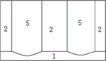
图2是采用本发明方法制备的超级结器件的结构示意图。Fig. 2 is a schematic structural view of a super junction device prepared by the method of the present invention.
其中,1.是N型硅基板(110晶面),2是N型外延层,3是介质膜,4是光刻胶,5是P型外延层,6是P阱区,7是N+阱区,8是P+源区,9是层间介质膜,10是背面漏金属电极,11是正面源金属电极,12是多晶硅,13是栅氧。Among them, 1. is the N-type silicon substrate (110 crystal plane), 2 is the N-type epitaxial layer, 3 is the dielectric film, 4 is the photoresist, 5 is the P-type epitaxial layer, 6 is the P well region, and 7 is the N+ well 8 is the P+ source region, 9 is the interlayer dielectric film, 10 is the back drain metal electrode, 11 is the front source metal electrode, 12 is polysilicon, and 13 is gate oxide.
具体实施方式Detailed ways
下面结合附图和实施例对本发明作进一步详细的说明。The present invention will be described in further detail below in conjunction with the accompanying drawings and embodiments.
如图1和图2所示,本发明使用湿法刻蚀制备超级结器件的方法的具体步骤包括如下:As shown in Figures 1 and 2, the specific steps of the method for preparing a super junction device using wet etching in the present invention include the following:
(1)在110晶面(晶面取向110)的N型硅基板1上成长N型外延层2,N型外延层2的厚度在5-80um(微米)之间,见图1A;(1) An N-type epitaxial layer 2 is grown on an N-
(2)在硅片的正面和背面同时形成介质膜3,可以使用扩散的方法形成热氧化膜作为介质膜3,其厚度在1000埃-5000埃之间,也可使用LPCVD(低压化学气相沉积工艺)形成氧化膜或氮化膜作为介质膜3,氧化膜的厚度在2000埃-10000埃之间,氮化膜的厚度可以在100埃-500埃之间,见图1B;(2)
(3)正面用光刻胶4定义图形,光刻板的设计图形开口与111晶面(晶面取向111,见图1C和图1D中深沟槽侧面的晶面)对齐,用干法刻蚀的方法打开介质膜3,见图1C;(3) The photoresist 4 is used to define the pattern on the front side, and the design pattern opening of the photoresist plate is aligned with the 111 crystal plane (crystal plane orientation 111, see the crystal plane on the side of the deep trench in Figure 1C and Figure 1D), and dry etching The method to open the
(4)去除光刻胶4,可以使用ashing(灰化)或者SPM(硫酸双氧水)混合物来去除光刻胶;利用介质膜3作为掩膜层,使用湿法各向异性刻蚀形成垂直的深沟槽结构,背面的介质膜3起到保护背面单晶硅的作用,正面形成垂直的深沟槽结构(深沟槽的深度可以为5um-50um),湿法药液可使用KOH(氢氧化钾),TMAH(四甲基氢氧铵)或EDP(邻苯二酚乙二胺)等碱性溶液,与去离子水的重量百分比为1%-50%,湿法药液也可以使用上述的碱性溶液与IPA(异丙醇)的混合药液,IPA与碱性溶液的体积百分比比例为1%-30%,见图1D;(4) To remove the photoresist 4, you can use ashing (ashing) or SPM (sulfuric acid hydrogen peroxide) mixture to remove the photoresist; use the
(5)清洗(清洗采用硫酸双氧水+稀释氢氟酸+氨水双氧水+盐酸双氧水的湿法工艺)和P型外延层5在深沟槽内填充成长形成交替排列的P型和N型的结构,见图1E;(5) Cleaning (wet process of sulfuric acid hydrogen peroxide + diluted hydrofluoric acid + ammonia hydrogen peroxide + hydrochloric acid hydrogen peroxide) and P-type epitaxial layer 5 is filled and grown in the deep trench to form alternately arranged P-type and N-type structures, See Figure 1E;
(6)使用化学机械抛光的方法进行平坦化处理,停在介质膜3上,见图1F;(6) Perform planarization by chemical mechanical polishing, and stop on the
(7)利用湿法刻蚀去除正反面的介质膜3,即可形成P型和N型交替排列的结构,如果介质膜3是氧化膜,湿法药液可使用BOE(缓冲氧化膜刻蚀剂)或HF(氢氟酸),如果介质膜3是氮化膜,湿法药液可使用热磷酸,见图1G;(7) Use wet etching to remove the
(8)后续工艺可采用成熟的纵向双扩散金属氧化物半导体即可制备完整的超级结器件,见图2。后续工艺的步骤具体如下:(8) The subsequent process can use the mature vertical double-diffused metal oxide semiconductor to prepare a complete super junction device, as shown in Figure 2. The steps of the follow-up process are as follows:
A.使用离子注入的方式分别在特定图形部分形成P阱区6(可采用硼注入),N+阱区7(可采用磷或者砷注入),P+源区8(可采用硼注入);A. Use ion implantation to form P well region 6 (boron implantation can be used), N+ well region 7 (phosphorus or arsenic implantation can be used), and P+ source region 8 (boron implantation can be used) in specific pattern parts respectively;
B.使用扩散方式形成栅氧13,再使用低压化学气相沉积法淀积多晶硅12,并进行干法刻蚀,在特定图形部分形成多晶硅栅电极;B. Form gate oxide 13 by diffusion, then deposit polysilicon 12 by low-pressure chemical vapor deposition, and perform dry etching to form polysilicon gate electrodes in specific pattern parts;
C.使用低压化学气相沉积法,常压化学气相沉积法或等离子增强化学气相沉积法形成层间介质膜9,层间介质膜9的种类是氧化膜,随后进行干法刻蚀,形成多晶硅和金属电极的层间隔离以及源区和金属电极的接触孔;C. Use low-pressure chemical vapor deposition, atmospheric pressure chemical vapor deposition or plasma-enhanced chemical vapor deposition to form interlayer dielectric film 9. The type of interlayer dielectric film 9 is an oxide film, followed by dry etching to form polysilicon and Interlayer isolation of metal electrodes and contact holes for source regions and metal electrodes;
D.在硅片正面采用溅射物理气相沉积法形成正面源金属电极11;D. Forming the front source metal electrode 11 on the front side of the silicon wafer by sputtering physical vapor deposition;
E.在硅片背面采用蒸发物理气相沉积法形成背面漏金属电极10。E. Forming the back drain metal electrode 10 on the back of the silicon wafer by evaporative physical vapor deposition.
本发明利用在单晶硅上由于晶面不同取向的面上湿法的各向异性刻蚀,利用湿法刻蚀的方法在N型外延层上开垂直的深沟槽,通常在晶面取向110的硅基板上进行各向异性的湿法刻蚀,可形成垂直的深沟槽,深沟槽侧面的晶面为111,这样做的好处如下:1.湿法刻蚀对硅基板损伤较小,能保证后续的外延层生长质量较好,减少PN结界面的缺陷,降低漏电流;2.湿法刻蚀的生产成本较低;3.湿法刻蚀是由晶面取向控制刻蚀速率的,可保证深沟槽的90度的垂直形貌和面内形貌的均匀性。The present invention utilizes the wet anisotropic etching on the surface of the single crystal silicon due to the different orientations of the crystal planes, and uses the wet etching method to open vertical deep grooves on the N-type epitaxial layer, usually in the crystal plane orientation Anisotropic wet etching on the 110 silicon substrate can form vertical deep grooves, and the crystal plane on the side of the deep groove is 111. The advantages of this are as follows: 1. Wet etching is less damaging to the silicon substrate Small, can ensure better growth quality of the subsequent epitaxial layer, reduce defects at the PN junction interface, and reduce leakage current; 2. The production cost of wet etching is low; 3. Wet etching is controlled by crystal plane orientation The speed can guarantee the 90-degree vertical shape of the deep trench and the uniformity of the in-plane shape.
Claims (9)
Priority Applications (1)
| Application Number | Priority Date | Filing Date | Title |
|---|---|---|---|
| CN201010276031.1ACN102403216B (en) | 2010-09-09 | 2010-09-09 | Wet etching method for preparation of super-junction device |
Applications Claiming Priority (1)
| Application Number | Priority Date | Filing Date | Title |
|---|---|---|---|
| CN201010276031.1ACN102403216B (en) | 2010-09-09 | 2010-09-09 | Wet etching method for preparation of super-junction device |
Publications (2)
| Publication Number | Publication Date |
|---|---|
| CN102403216A CN102403216A (en) | 2012-04-04 |
| CN102403216Btrue CN102403216B (en) | 2013-06-12 |
Family
ID=45885296
Family Applications (1)
| Application Number | Title | Priority Date | Filing Date |
|---|---|---|---|
| CN201010276031.1AActiveCN102403216B (en) | 2010-09-09 | 2010-09-09 | Wet etching method for preparation of super-junction device |
Country Status (1)
| Country | Link |
|---|---|
| CN (1) | CN102403216B (en) |
Families Citing this family (5)
| Publication number | Priority date | Publication date | Assignee | Title |
|---|---|---|---|---|
| CN102931299B (en)* | 2012-11-20 | 2017-05-10 | 无锡华润华晶微电子有限公司 | Laser etching method for light-emitting diode |
| CN103021817B (en)* | 2012-12-27 | 2017-12-08 | 上海集成电路研发中心有限公司 | Cleaning method after wet etching |
| CN109698131B (en)* | 2019-01-30 | 2022-06-17 | 上海华虹宏力半导体制造有限公司 | Wafer back process method of super junction device |
| CN113594024B (en)* | 2021-07-30 | 2024-01-30 | 中国电子科技集团公司第四十四研究所 | Method for producing metal electrode stripping film and method for producing metal stripping electrode |
| CN117476468B (en)* | 2023-12-26 | 2024-03-22 | 北京智芯微电子科技有限公司 | Super junction structure, manufacturing method thereof, super junction semiconductor device and semiconductor structure |
Family Cites Families (4)
| Publication number | Priority date | Publication date | Assignee | Title |
|---|---|---|---|---|
| JP4728508B2 (en)* | 2001-06-11 | 2011-07-20 | 株式会社東芝 | Method for manufacturing vertical power semiconductor device |
| JP5150048B2 (en)* | 2005-09-29 | 2013-02-20 | 株式会社デンソー | Manufacturing method of semiconductor substrate |
| US7598517B2 (en)* | 2006-08-25 | 2009-10-06 | Freescale Semiconductor, Inc. | Superjunction trench device and method |
| JP5261641B2 (en)* | 2007-09-13 | 2013-08-14 | セミコンダクター・コンポーネンツ・インダストリーズ・リミテッド・ライアビリティ・カンパニー | Manufacturing method of semiconductor wafer |
- 2010
- 2010-09-09CNCN201010276031.1Apatent/CN102403216B/enactiveActive
Also Published As
| Publication number | Publication date |
|---|---|
| CN102403216A (en) | 2012-04-04 |
Similar Documents
| Publication | Publication Date | Title |
|---|---|---|
| CN103681355B (en) | Prepare the method for accurate SOI source-drain field effect transistor device | |
| CN102403216B (en) | Wet etching method for preparation of super-junction device | |
| CN101916784B (en) | SOI (Silicon on Insulator) variable buried oxide layer thickness device and preparation method thereof | |
| CN105489500B (en) | The preparation method and its hyperconjugation VDMOS device of hyperconjugation VDMOS | |
| CN101996922B (en) | Silicon on insulator (SOI) wafer and formation method thereof | |
| CN108735605A (en) | Improve the shield grid groove MOSFET manufacturing method of channel bottom field plate pattern | |
| CN100536092C (en) | Method for manufacturing fin-shaped field effect transistor by epitaxial process | |
| CN104347346B (en) | The deep trench flattening method of different structure | |
| CN105575781B (en) | The manufacturing method of groove-shaped super junction | |
| CN102403257A (en) | Method for Improving the Etched Boundary Morphology of Deep Trench of Super Junction Devices | |
| CN104112670B (en) | A kind of semiconductor devices and preparation method thereof | |
| CN114512406A (en) | Manufacturing method of superjunction device | |
| CN102832121B (en) | fast recovery diode manufacturing method | |
| CN102856200A (en) | Method for forming PN column layer of super node MOSFET (Metal-Oxide-Semiconductor Field Effect Transistor) | |
| WO2014040360A1 (en) | High-voltage super-junction igbt manufacturing method | |
| CN104282550A (en) | Method for manufacturing Schottky diode | |
| CN112285827A (en) | Preparation method of multilayer silicon photonic device | |
| CN111834286A (en) | Semiconductor insulating substrate, transistor and preparation method thereof | |
| CN102479699B (en) | Manufacturing method of super-junction semiconductor device structure | |
| CN103928386B (en) | A kind of manufacture method of fleet plough groove isolation structure | |
| CN115579326A (en) | Method for manufacturing semiconductor integrated circuit | |
| CN111508834A (en) | Manufacturing method of silicon-based photodetector | |
| CN106816376A (en) | Preparation method of super junction device voltage-resistant layer | |
| CN100539048C (en) | A kind of method of making quasi double grids MOSFET transistor | |
| CN106784019A (en) | A kind of Ge bases solid state plasma PiN diodes and preparation method thereof |
Legal Events
| Date | Code | Title | Description |
|---|---|---|---|
| C06 | Publication | ||
| PB01 | Publication | ||
| C10 | Entry into substantive examination | ||
| SE01 | Entry into force of request for substantive examination | ||
| C14 | Grant of patent or utility model | ||
| GR01 | Patent grant | ||
| ASS | Succession or assignment of patent right | Owner name:SHANGHAI HUAHONG GRACE SEMICONDUCTOR MANUFACTURING Free format text:FORMER OWNER: HUAHONG NEC ELECTRONICS CO LTD, SHANGHAI Effective date:20131219 | |
| C41 | Transfer of patent application or patent right or utility model | ||
| COR | Change of bibliographic data | Free format text:CORRECT: ADDRESS; FROM: 201206 PUDONG NEW AREA, SHANGHAI TO: 201203 PUDONG NEW AREA, SHANGHAI | |
| TR01 | Transfer of patent right | Effective date of registration:20131219 Address after:201203 Shanghai city Zuchongzhi road Pudong New Area Zhangjiang hi tech Park No. 1399 Patentee after:Shanghai Huahong Grace Semiconductor Manufacturing Corporation Address before:201206, Shanghai, Pudong New Area, Sichuan Road, No. 1188 Bridge Patentee before:Shanghai Huahong NEC Electronics Co., Ltd. |