CN102394334A - Multiband resonator and multiband-pass filter - Google Patents
Multiband resonator and multiband-pass filterDownload PDFInfo
- Publication number
- CN102394334A CN102394334ACN2011101783397ACN201110178339ACN102394334ACN 102394334 ACN102394334 ACN 102394334ACN 2011101783397 ACN2011101783397 ACN 2011101783397ACN 201110178339 ACN201110178339 ACN 201110178339ACN 102394334 ACN102394334 ACN 102394334A
- Authority
- CN
- China
- Prior art keywords
- conductor
- line conductor
- main
- dielectric layer
- open stub
- Prior art date
- Legal status (The legal status is an assumption and is not a legal conclusion. Google has not performed a legal analysis and makes no representation as to the accuracy of the status listed.)
- Granted
Links
Images


Classifications
- H—ELECTRICITY
- H01—ELECTRIC ELEMENTS
- H01P—WAVEGUIDES; RESONATORS, LINES, OR OTHER DEVICES OF THE WAVEGUIDE TYPE
- H01P1/00—Auxiliary devices
- H01P1/20—Frequency-selective devices, e.g. filters
- H01P1/201—Filters for transverse electromagnetic waves
- H01P1/203—Strip line filters
- H01P1/20327—Electromagnetic interstage coupling
- H01P1/20336—Comb or interdigital filters
- H01P1/20345—Multilayer filters
- H—ELECTRICITY
- H01—ELECTRIC ELEMENTS
- H01P—WAVEGUIDES; RESONATORS, LINES, OR OTHER DEVICES OF THE WAVEGUIDE TYPE
- H01P7/00—Resonators of the waveguide type
- H01P7/08—Strip line resonators
- H—ELECTRICITY
- H03—ELECTRONIC CIRCUITRY
- H03H—IMPEDANCE NETWORKS, e.g. RESONANT CIRCUITS; RESONATORS
- H03H7/00—Multiple-port networks comprising only passive electrical elements as network components
- H03H7/01—Frequency selective two-port networks
- H03H7/0115—Frequency selective two-port networks comprising only inductors and capacitors
- H—ELECTRICITY
- H01—ELECTRIC ELEMENTS
- H01P—WAVEGUIDES; RESONATORS, LINES, OR OTHER DEVICES OF THE WAVEGUIDE TYPE
- H01P1/00—Auxiliary devices
- H01P1/20—Frequency-selective devices, e.g. filters
- H01P1/201—Filters for transverse electromagnetic waves
- H01P1/203—Strip line filters
- H—ELECTRICITY
- H01—ELECTRIC ELEMENTS
- H01P—WAVEGUIDES; RESONATORS, LINES, OR OTHER DEVICES OF THE WAVEGUIDE TYPE
- H01P1/00—Auxiliary devices
- H01P1/20—Frequency-selective devices, e.g. filters
- H01P1/213—Frequency-selective devices, e.g. filters combining or separating two or more different frequencies
- H01P1/2135—Frequency-selective devices, e.g. filters combining or separating two or more different frequencies using strip line filters
- H—ELECTRICITY
- H01—ELECTRIC ELEMENTS
- H01P—WAVEGUIDES; RESONATORS, LINES, OR OTHER DEVICES OF THE WAVEGUIDE TYPE
- H01P7/00—Resonators of the waveguide type
- H01P7/10—Dielectric resonators
- H—ELECTRICITY
- H03—ELECTRONIC CIRCUITRY
- H03H—IMPEDANCE NETWORKS, e.g. RESONANT CIRCUITS; RESONATORS
- H03H7/00—Multiple-port networks comprising only passive electrical elements as network components
- H03H7/01—Frequency selective two-port networks
- H03H7/17—Structural details of sub-circuits of frequency selective networks
- H03H7/1741—Comprising typical LC combinations, irrespective of presence and location of additional resistors
- H03H7/1766—Parallel LC in series path
Landscapes
- Physics & Mathematics (AREA)
- Electromagnetism (AREA)
- Engineering & Computer Science (AREA)
- Power Engineering (AREA)
- Control Of Motors That Do Not Use Commutators (AREA)
Abstract
Translated fromChinese
Description
Translated fromChinese技术领域technical field
本发明涉及具有多个谐振频率的多频带谐振器(multiband resonator)和利用了该多频带谐振器的多带通滤波器(multiband-pass filter),特别涉及在移动通信、卫星通信、固定微波通信、以及其他的通信技术领域中用于信号的发送接收的多频带谐振器和多带通滤波器。The present invention relates to a multiband resonator (multiband resonator) with multiple resonant frequencies and a multiband-pass filter (multiband-pass filter) utilizing the multiband resonator, particularly in mobile communications, satellite communications, and fixed microwave communications , and other multi-band resonators and multi-bandpass filters used for signal transmission and reception in the field of communication technology.
背景技术Background technique
作为具有多个谐振频率的多频带谐振器,非专利文献1(S.Kitazawa,H.Miyake,M.Geshiro,and M.Ohashi,″A MultilayerSigle-Imput/Single-OutputDual-Band Filer Fabricated in a High PermittivityLTCC Substrate,″IEICE Trans.Electron.,vol.E89-C,no.4,pp.509-516,April2006.)的多频带谐振器作为以往技术而已知。该多频带谐振器是经由屏蔽层而层叠了具有不同的一个谐振频率的两个谐振器的结构。并且,这些谐振器与输入输出端口耦合而构成多频带的谐振器。另外,作为具有一个谐振频率的谐振器,公开了各种谐振器,例如有如非专利文献2(吉田賢太郎,北村敏明,下代雅啓,石崎俊雄,″折返し形コムラインフイルタの特性解析,″電子情報通信学会論文誌C,vol.J86-C,no.4,pp.442-449,April 2003.)这样的谐振器。As a multi-band resonator with multiple resonant frequencies, Non-Patent Document 1 (S. Kitazawa, H. Miyake, M. Geshiro, and M. Ohashi, "A Multilayer Sigle-Imput/Single-Output Dual-Band Filer Fabricated in a High Permittivity LTCC Substrate, "IEICE Trans. Electron., vol. E89-C, no. 4, pp. 509-516, April 2006.) multi-band resonators are known as prior art. This multiband resonator has a structure in which two resonators having different one resonant frequency are laminated via a shield layer. Furthermore, these resonators are coupled to the input and output ports to form a multi-band resonator. In addition, various resonators have been disclosed as resonators having one resonant frequency, for example, non-patent literature 2 (Kentaro Yoshida, Toshiaki Kitamura, Masaki Shimodai, Toshio Ishizaki, "Analysis of the characteristics of the turn-back ししししししなんどんんイルタの," Electronic Information and Communication Society Journal C, vol. J86-C, no.4, pp.442-449, April 2003.) Such a resonator.
但是,在以往技术中,为了获得多个谐振频率,经由屏蔽层而层叠了具有不同的谐振频率的谐振器。即,是将独立的谐振器以不会互相受到影响的状态集成的谐振器。因此,存在层数容易增加且难以小型化的课题。However, in the prior art, in order to obtain a plurality of resonance frequencies, resonators having different resonance frequencies are stacked via shield layers. That is, it is a resonator in which independent resonators are integrated in a state that does not affect each other. Therefore, there is a problem that the number of layers is easy to increase and miniaturization is difficult.
发明内容Contents of the invention
本发明的目的在于,将具有多个谐振频率的多频带谐振器小型化。An object of the present invention is to miniaturize a multiband resonator having a plurality of resonance frequencies.
本发明的多频带谐振器包括电介质基板、地导体、主线路导体、副线路导体、副开路短截线、主开路短截线、短路导体、主贯通导体、副贯通导体。电介质基板具有3个以上的电介质层。地导体既可以形成在其中一个电介质层上,也可以形成为覆盖电介质基板整体。主线路导体和副线路导体在其中一个电介质层上形成。副开路短截线在与主线路导体和副线路导体不同的电介质层上形成。主开路短截线在与主线路导体、副线路导体以及副开路短截线不同的电介质层上形成。短路导体将主线路导体的一端和副线路导体的一端电连接,且还与地导体电连接。主贯通导体将主线路导体的另一端和与该主线路导体的另一端对置的主开路短截线的一端电连接。副贯通导体将副线路导体的另一端和与该副线路导体的另一端对置的副开路短截线的一端电连接。The multi-band resonator of the present invention includes a dielectric substrate, a ground conductor, a main line conductor, an auxiliary line conductor, an auxiliary open stub, a main open stub, a short circuit conductor, a main through conductor, and an auxiliary through conductor. The dielectric substrate has three or more dielectric layers. The ground conductor may be formed on one of the dielectric layers, or may be formed to cover the entire dielectric substrate. A main line conductor and a sub line conductor are formed on one of the dielectric layers. The secondary open stub is formed on a different dielectric layer than the primary and secondary line conductors. The primary open stub is formed on a different dielectric layer than the primary line conductor, secondary line conductor, and secondary open stub. The short-circuit conductor electrically connects one end of the main line conductor and one end of the sub-line conductor, and is also electrically connected to the ground conductor. The main through-conductor electrically connects the other end of the main line conductor to one end of the main open stub opposed to the other end of the main line conductor. The sub-through conductor electrically connects the other end of the sub-line conductor to one end of the sub-open stub opposed to the other end of the sub-line conductor.
并且,主线路导体和副线路导体既可以形成在不同的电介质层上,也可以形成在同一个电介质层上。在主线路导体和副线路导体形成在不同的电介质层上的情况下,电介质基板至少具有第1至第4电介质层。并且,作为短路导体,使用基本贯通导体即可。基本贯通导体将若干个电介质层贯通,从而将主线路导体的一端和与该主线路导体的一端对置的副线路导体的一端电连接,且还与地导体电连接。此外,在主线路导体和副线路导体形成在同一个电介质层上的情况下,电介质基板至少具有第1至第3电介质层。并且,作为短路导体,使用第1短路线路导体即可。第1短路线路导体在与主线路导体和副线路导体所形成的电介质层相同的电介质层上形成,将主线路导体的一端和副线路导体的一端电连接,且还与地导体电连接。Furthermore, the main line conductor and the sub line conductor may be formed on different dielectric layers, or may be formed on the same dielectric layer. When the main line conductor and the sub line conductor are formed on different dielectric layers, the dielectric substrate has at least first to fourth dielectric layers. In addition, as the short-circuit conductor, a substantially through-conductor may be used. The basic through-conductor penetrates the plurality of dielectric layers, thereby electrically connecting one end of the main line conductor to one end of the sub-line conductor opposite to the one end of the main line conductor, and is also electrically connected to the ground conductor. In addition, when the main line conductor and the sub line conductor are formed on the same dielectric layer, the dielectric substrate has at least first to third dielectric layers. In addition, as the short-circuit conductor, the first short-circuit line conductor may be used. The first short-circuit conductor is formed on the same dielectric layer as that formed by the main-line conductor and the sub-line conductor, electrically connects one end of the main-line conductor and one end of the sub-line conductor, and is also electrically connected to the ground conductor.
这里,“对置”意味着从电介质基板的面的法线方向看电介质基板时(从平面上方看时)位于相互大致重叠的位置。此外,本发明的多带通滤波器作为谐振器而包括多个本发明的多频带谐振器,且包括输入用的输入输出线路导体和输出用的输入输出线路导体。Here, "opposite" means that the dielectric substrates are positioned substantially overlapping with each other when viewed from the normal direction of the surface of the dielectric substrate (when viewed from above the plane). Furthermore, the multi-bandpass filter of the present invention includes a plurality of multi-band resonators of the present invention as resonators, and includes an input-output line conductor for input and an input-output line conductor for output.
由于共享各个结构部分而(一体地)构成具有多个谐振频率的谐振器,所以能够将本发明的多频带谐振器小型化。此外,由于使用本发明的多频带谐振器而构成,所以能够将本发明的多带通滤波器小型化。Since a resonator having a plurality of resonant frequencies is constituted (integrally) by sharing each structural part, the multi-band resonator of the present invention can be miniaturized. Furthermore, since it is configured using the multiband resonator of the present invention, the multiband pass filter of the present invention can be miniaturized.
附图说明Description of drawings
图1是表示实施例1的多频带谐振器的结构例的立体图。FIG. 1 is a perspective view showing a configuration example of a multiband resonator according to
图2是实施例1的多频带谐振器的展开立体图。FIG. 2 is an expanded perspective view of the multi-band resonator of
图3是用于说明本发明的原理的展开立体图。Fig. 3 is a developed perspective view for explaining the principle of the present invention.
图4是实施例1的变形例1的多频带谐振器的展开立体图。4 is a developed perspective view of a multiband resonator according to
图5是实施例1的变形例2的多频带谐振器的展开立体图。5 is a developed perspective view of a multi-band resonator according to
图6是实施例1的变形例3的多频带谐振器的展开立体图。FIG. 6 is a developed perspective view of a multiband resonator according to
图7是实施例1的变形例4的多频带谐振器的展开立体图。7 is a developed perspective view of a multiband resonator according to
图8是实施例1的变形例5的多频带谐振器的展开立体图。8 is a developed perspective view of a multi-band resonator according to
图9是实施例1的变形例6的多频带谐振器的展开立体图。9 is a developed perspective view of a multi-band resonator according to
图10是实施例1的变形例7的多频带谐振器的展开立体图。10 is a developed perspective view of a multiband resonator according to
图11是实施例1的变形例8的多频带谐振器的展开立体图。11 is a developed perspective view of a multi-band resonator according to
图12是实施例1的变形例9的多频带谐振器的展开立体图。12 is a developed perspective view of a multi-band resonator according to
图13是表示第1模拟的多带通滤波器的结构的图。FIG. 13 is a diagram showing the configuration of a first analog multi-bandpass filter.
图14是表示图13的多带通滤波器的频率响应的模拟结果的图。FIG. 14 is a diagram showing simulation results of the frequency response of the multi-bandpass filter of FIG. 13 .
图15是表示第2模拟的多带通滤波器的结构的图。FIG. 15 is a diagram showing the configuration of a second analog multi-bandpass filter.
图16是表示图15的多带通滤波器的频率响应的模拟结果的图。FIG. 16 is a graph showing simulation results of the frequency response of the multi-bandpass filter of FIG. 15 .
图17是表示第3模拟的多带通滤波器的结构的图。FIG. 17 is a diagram showing the configuration of a third analog multi-bandpass filter.
图18是表示图17的多带通滤波器的频率响应的模拟结果的图。FIG. 18 is a graph showing simulation results of the frequency response of the multi-bandpass filter of FIG. 17 .
图19是实施例2的多频带谐振器的展开立体图。FIG. 19 is an expanded perspective view of a multiband resonator according to
图20是实施例2的变形例1的多频带谐振器的展开立体图。20 is a developed perspective view of a multiband resonator according to
图21是实施例2的变形例2的多频带谐振器的展开立体图。FIG. 21 is a developed perspective view of a multiband resonator according to
图22是实施例2的变形例3的多频带谐振器的展开立体图。22 is a developed perspective view of a multi-band resonator according to
图23是实施例2的变形例4的多频带谐振器的展开立体图。23 is a developed perspective view of a multiband resonator according to
图24A是表示第4模拟的多带通滤波器的结构的俯视图。FIG. 24A is a plan view showing the configuration of a fourth analog multi-bandpass filter.
图24B是从底往上看第4模拟的多带通滤波器的图。Fig. 24B is a bottom-up view of the fourth analog multi-bandpass filter.
图25是表示在图24A和图24B所示的多带通滤波器的频率响应的模拟结果的图。FIG. 25 is a graph showing simulation results of the frequency response of the multi-bandpass filter shown in FIGS. 24A and 24B .
图26A是表示第5模拟的多带通滤波器的结构的俯视图。FIG. 26A is a plan view showing the configuration of a fifth analog multi-bandpass filter.
图26B是表示第5模拟的多带通滤波器的结构的、从不同的角度看的俯视图。FIG. 26B is a plan view from a different angle showing the configuration of the fifth analog multi-bandpass filter.
图27是表示在图26A和图26B所示的多带通滤波器的频率响应的模拟结果的图。FIG. 27 is a diagram showing simulation results of the frequency response of the multi-bandpass filter shown in FIGS. 26A and 26B .
图28是表示第6模拟的多带通滤波器的结构的俯视图。FIG. 28 is a plan view showing the configuration of a sixth simulation multi-bandpass filter.
图29是表示在图28所示的多带通滤波器的频率响应的模拟结果的图。FIG. 29 is a graph showing simulation results of the frequency response of the multi-bandpass filter shown in FIG. 28 .
图30A是表示第7模拟的多带通滤波器的结构的俯视图。FIG. 30A is a plan view showing the configuration of a seventh analog multi-bandpass filter.
图30B是表示第7模拟的多带通滤波器的结构的、从不同的角度看的俯视图。30B is a plan view from a different angle showing the structure of the multi-bandpass filter of the seventh simulation.
图31是表示在图30A和图30B所示的多带通滤波器的频率响应的模拟结果的图。Fig. 31 is a graph showing simulation results of the frequency response of the multi-bandpass filter shown in Figs. 30A and 30B.
标号说明Label description
100、101、102、103、104、105、106、107、108、300、301、302、303多频带谐振器100, 101, 102, 103, 104, 105, 106, 107, 108, 300, 301, 302, 303 multi-band resonators
110、112、113、114、117、118基本贯通导体110, 112, 113, 114, 117, 118 basic through conductors
120、122、123、124主贯通导体120, 122, 123, 124 main through conductor
130、131、132、134、136副贯通导体130, 131, 132, 134, 136 through conductors
143第2副贯通导体143 Second through conductor
146耦合导体(coupling conductor)146 coupling conductor (coupling conductor)
150、151地导体150, 151 ground conductor
157、158、159输入输出线路导体157, 158, 159 input and output line conductors
160主线路导体160 main line conductor
169主开关169 main switch
170、171、174副线路导体170, 171, 174 pair of line conductors
173第2副线路导体173 Secondary line conductor
179副开关179 sub-switches
180、181、184主开路短截线180, 181, 184 main open circuit stubs
190、191、194副开路短截线190, 191, 194 pairs of open circuit stubs
193第2副开路短截线193 2nd pair of open circuit stubs
210、212、213、214、217电介质层210, 212, 213, 214, 217 dielectric layer
220、222、223、224、227、228、229电介质基板220, 222, 223, 224, 227, 228, 229 dielectric substrate
311、312、313、314、315短路线路导体311, 312, 313, 314, 315 short circuit conductors
321短路贯通导体321 short-circuit through conductor
1171、1172、1173、1174、1175、1181贯通导体1171, 1172, 1173, 1174, 1175, 1181 through conductor
1176、1177、1178、1179、1182线路导体1176, 1177, 1178, 1179, 1182 line conductors
具体实施方式Detailed ways
以下,详细说明本发明的实施方式。另外,对于具有相同的功能的结构部分赋予相同的标号,省略重复说明。Embodiments of the present invention will be described in detail below. In addition, the same code|symbol is attached|subjected to the structural part which has the same function, and repeated description is abbreviate|omitted.
【实施例1】【Example 1】
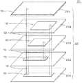
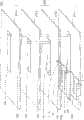
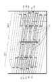
图1是表示实施例1的多频带谐振器的结构例的立体图,图2是实施例1的多频带谐振器的展开立体图。在这些图中,为了能够看到各个结构部分,透明地描画了各个结构部分。但是,应注意各个结构部分并不需要是透明的,大多数情况下使用不透明的材料。此外,在图2的展开立体图中,基本贯通导体110、主贯通导体120、副贯通导体130随着将电介质层之间远离绘制而拉长,但实际上是如图1所示那样与一个或者多个电介质层的厚度相同的长度。图3是用于说明本发明的原理的展开立体图。另外,在这些图中,省略了输入输出线路,但例如与主线路导体形成在同一个面即可。FIG. 1 is a perspective view showing a structural example of the multiband resonator of the first embodiment, and FIG. 2 is an expanded perspective view of the multiband resonator of the first embodiment. In these figures, each structural part is drawn transparently so that each structural part can be seen. However, it should be noted that the individual structural parts do not need to be transparent, in most cases opaque materials are used. In addition, in the developed perspective view of FIG. 2 , the basic through-
多频带谐振器100包括:具有第1至第5电介质层210-1、......、5的电介质基板220;形成在第1电介质层210-1上的主线路导体160;形成在第2电介质层210-2上的副线路导体170;形成在第3电介质层210-3上的副开路短截线190;形成在第4电介质层210-4上的主开路短截线180;形成在第5电介质层210-5上的地导体150;基本贯通导体110;主贯通导体120;以及副贯通导体130。基本贯通导体110将主线路导体160的一端B和与主线路导体160的一端B对置的副线路导体170的一端F电连接,且还与地导体150电连接。主贯通导体120将主线路导体160的另一端C和与主线路导体160的另一端C对置的主开路短截线180的一端D电连接。副贯通导体130将副线路导体170的另一端G和与副线路导体170的另一端G对置的副开路短截线190的一端H电连接。这里,“对置”意味着从电介质基板220的面的法线方向看电介质基板220时(从平面上方看时)位于相互大致重叠的位置。The
图3中用实线表示的是形成了第1谐振模式310的部分。认为第1谐振模式是从与地导体150连接的点A(短路点)至主开路短截线180的开路端E为止的电长(A-F-B-C-D-E)大约成为1/4波长的谐振。此外,图3中用虚线表示的是形成了第2谐振模式320的部分。认为第2谐振模式是从与地导体150连接的点A(短路点)至副开路短截线190的开路端I为止的电长(A-F-G-H-I)大约成为1/4波长的谐振。The portion where the first resonance mode 310 is formed is indicated by a solid line in FIG. 3 . The first resonance mode is considered to be resonance in which the electrical length (A-F-B-C-D-E) from point A (short-circuit point) connected to
由于多频带谐振器100为这样的结构和原理,所以能够将具有多个谐振频率的多频带谐振器以共享各个结构部分的状态(一体地)构成。因此,能够将多频带谐振器100小型化。此外,可根据电介质层的厚度和介电常数、主线路导体160和主开路短截线180、副线路导体170和副开路短截线190的长度,调整谐振频率(在由该多频带谐振器形成了多带通滤波器的情况下是通过频率(passband))。另外,在图1~3中,电介质层从第1至第5按顺序排列。但并不需要一定限定为这个顺序,只要是为了调整而适当地设计即可。此外,在图1~3中,使主开路短截线180的另一端E和副开路短截线190的另一端I对置。但并不需要一定对置,只要是为了调整而适当地设计即可。此外,也可以在主线路导体160的另一端C和地导体151之间包括LC并联谐振电路。LC并联谐振电路也可以是集总参数元件。LC并联谐振电路是成为基本贯通导体的替代的电路。在将LC并联谐振电路认为是谐振部件的情况下,LC并联谐振电路对谐振频率产生影响。此外,在设置输入输出线路的基础上,将LC并联谐振电路认为是滤波器部件的情况下,LC并联谐振电路还对输入输出匹配产生影响。此外,通过作为谐振部而包括多个多频带谐振器100,且在其中两个谐振部中设置连接到主线路导体的输入输出线路导体,从而能够形成多带通滤波器。Since the
【变形例1】【Modification 1】
图4是实施例1的变形例1的多频带谐振器的展开立体图。在该图中,也为了能够看到各个结构部分,透明地描画了各个结构部分。此外,在图4的展开立体图中,基本贯通导体110、主贯通导体120、副贯通导体130随着将电介质层之间远离绘制而拉长,但实际上也是如图1所示那样与一个或者多个电介质层的厚度相同的长度。另外,在这些图中,省略了输入输出线路,但例如与主线路导体形成在同一个面即可。4 is a developed perspective view of a multiband resonator according to
多频带谐振器100’是在多频带谐振器100中还附加了主开关169和副开关179的结构。主开关169形成在主线路导体160的一端,将主线路导体160和基本贯通导体110设为电接通状态(连接的状态)或者断开状态(切断的状态)。副开关179形成在副线路导体170的一端,将副线路导体170和基本贯通导体110设为电接通状态(连接的状态)或者断开状态(切断的状态)。在将主开关169和副开关179的两个都设为接通状态时,多频带谐振器100’与多频带谐振器100相同地成为具有两个谐振频率的多频带谐振器。在将主开关169接通、将副开关179断开时,多频带谐振器100’成为仅具有由第1谐振模式产生的谐振频率的谐振器。此外,在将主开关断开、将副开关接通时,多频带谐振器100’成为仅具有由第2谐振模式产生的谐振频率的谐振器。The multiband resonator 100' has a configuration in which a
由于变形例1的多频带谐振器为这样的结构,所以能够作为具有多个谐振频率的多频带谐振器来动作的同时,也能够作为可选择谐振频率的谐振器来动作,并且,能够将谐振器小型化。此外,通过作为谐振部而包括多个多频带谐振器100’,且在其中两个谐振部中设置连接到主线路导体的输入输出线路导体,从而能够形成多带通滤波器。Since the multiband resonator of
【变形例2】【Modification 2】
图5是实施例1的变形例2的多频带谐振器的展开立体图。在该图中,也为了能够看到各个结构部分,透明地描画了各个结构部分,基本贯通导体110、主贯通导体120、副贯通导体130随着将电介质层之间远离绘制而拉长,但实际上是如图1所示那样与一个或者多个电介质层的厚度相同的长度。另外,在这些图中,省略了输入输出线路,但例如与主线路导体形成在同一个面即可。5 is a developed perspective view of a multi-band resonator according to
多频带谐振器101与多频带谐振器100的不同点在于,主开路短截线181的宽度比主线路导体160的宽度宽且副开路短截线191的宽度比副线路导体170的宽度宽的方面。其他方面与多频带谐振器100相同。The difference between the
由于变形例2的多频带谐振器为这样的结构,所以通过主开路短截线181和副开路短截线的宽度,也能够调整谐振频率。因此,能够将多频带谐振器小型化的同时,容易调整谐振频率。另外,本变形例能够与变形例1进行组合。此外,通过作为谐振部而包括多个多频带谐振器101,且在其中两个谐振部中设置连接到主线路导体的输入输出线路导体,从而能够形成多带通滤波器。Since the multiband resonator of
【变形例3】【Modification 3】
图6是实施例1的变形例3的多频带谐振器的展开立体图。在该图中,也为了能够看到各个结构部分,透明地描画了各个结构部分,基本贯通导体112、主贯通导体122、副贯通导体132随着将电介质层之间远离绘制而拉长,但实际上是如图1所示那样与一个或者多个电介质层的厚度相同的长度。另外,在这些图中,省略了输入输出线路,但例如与主线路导体形成在同一个面即可。FIG. 6 is a developed perspective view of a multiband resonator according to
多频带谐振器102与多频带谐振器100的不同点在于,在电介质基板222的电介质层210-1和210-2之间配置电介质层212-6,在电介质层210-2和210-3之间配置电介质层212-7,在电介质层210-3和210-4之间配置电介质层212-8的方面。其他方面与多频带谐振器100相同。The difference between the
由于变形例3的多频带谐振器为这样的结构,所以能够将多频带谐振器小型化的同时,容易调整主线路导体和副线路导体之间的电磁耦合量、主开路短截线和副开路短截线之间的电磁耦合量,且容易调整多频带谐振器的谐振频率或无负载Q值。另外,本变形例能够与变形例1或变形例2进行组合。此外,通过作为谐振部而包括多个多频带谐振器102,且在其中两个谐振部中设置连接到主线路导体的输入输出线路导体,从而能够形成多带通滤波器。Since the multiband resonator of
【变形例4】【Modification 4】
图7是实施例1的变形例4的多频带谐振器的展开立体图。在该图中,也为了能够看到各个结构部分,透明地描画了各个结构部分,基本贯通导体113、主贯通导体123、副贯通导体133、第2副贯通导体143随着将电介质层之间远离绘制而拉长,但实际上是如图1所示那样与一个或者多个电介质层的厚度相同的长度。另外,在这些图中,省略了输入输出线路,但例如与主线路导体形成在同一个面即可。7 is a developed perspective view of a multiband resonator according to
多频带谐振器103在电介质基板223的电介质层210-2和210-3之间配置电介质层213-6、213-7。并且,在电介质层213-6上形成有第2副线路导体173,在电介质层213-7上形成有第2副开路短截线193。此外,还包括将第2副线路导体173的另一端和与第2副线路导体173的另一端对置的第2副开路短截线193的一端电连接的第2副贯通导体143。并且,基本贯通导体113还和与主线路导体160的一端对置的第2副线路导体173的一端电连接。另外,为了防止与第2副线路导体173、第2副开路短截线193、第2副贯通导体143的混同,有时将副线路导体170、副开路短截线190、副贯通导体133称为第1副线路导体170、第1副开路短截线190、第1副贯通导体133。In the
由于变形例4的多频带谐振器为这样的结构,所以能够构成具有三个谐振频率的多频带谐振器,并且,能够小型化。另外,与其他实施例相同地,能够通过电介质层的厚度和介电常数、线路导体的长度和宽度,调整谐振频率。另外,本变形例能够与变形例1~3进行组合。此外,也可以通过增加电介质层、进一步增加副线路导体和副开路短截线和副贯通导体,从而构成具有4个以上的谐振模式的多频带谐振器。此外,通过作为谐振部而包括多个多频带谐振器103,且在其中两个谐振部中设置连接到主线路导体的输入输出线路导体,从而能够形成多带通滤波器。Since the multiband resonator according to
【变形例5】【Modification 5】
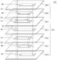
图8是实施例1的变形例5的多频带谐振器的展开立体图。在该图中,也为了能够看到各个结构部分,透明地描画了各个结构部分,基本贯通导体114、主贯通导体124、副贯通导体134随着将电介质层之间远离绘制而拉长,但实际上是如图1所示那样与一个或者多个电介质层的厚度相同的长度。另外,在这些图中,省略了输入输出线路,但例如形成在与主线路导体160同一个面即可。此外,在该图中省略了地导体。例如,附加了必要的电介质层的基础上,对于主线路导体160所形成的面成为对称地包括两个地导体即可。8 is a developed perspective view of a multi-band resonator according to
多频带谐振器104与多频带谐振器100的不同点在于,关于主线路导体160所形成的面成对称地形成两个副线路导体174、副开路短截线194、主开路短截线184。具体地说,电介质基板224以电介质层210-1为中心,层叠为电介质层214-4、214-3、214-2、210-1、214-2、214-3、214-4。主线路导体160形成在电介质层210-1上。两个副线路导体174分别形成在电介质层214-2上,两个副开路短截线194分别形成在电介质层214-3上,两个主开路短截线184分别形成在电介质层214-4上。The difference between
基本贯通导体114将主线路导体160的一端和与主线路导体160的一端对置的副线路导体174的一端电连接,且与地导体电连接。主线路导体124将主线路导体160的另一端和与主线路导体160的另一端对置的主开路短截线184的一端电连接。副贯通导体134将副线路导体174的另一端和与副线路导体174的另一端对置的副开路短截线194的一端电连接。另外,如上所述,“对置”意味着从电介质基板224的面的法线方向看电介质基板224时(从平面上方看时)位于相互大致重叠的位置。The basic through
变形例5的多频带谐振器的动作原理与实施例1相同,但由于关于主线路导体160所形成的面对称地形成两个副线路导体174、副开路短截线194、主开路短截线184,所以还能够获得抑制非对称结构产生的不需要的非对称谐振模式,还能够抑制期望的频率以外的谐振频率的产生。另外,本变形例也能够与其他的变形例进行组合,能够获得各自的优点。The operating principle of the multi-band resonator of
【变形例6】【Modification 6】
图9是实施例1的变形例6的多频带谐振器的展开立体图。在该图中,也为了能够看到各个结构部分,透明地描画了各个结构部分,基本贯通导体114、主贯通导体124、副贯通导体134随着将电介质层之间远离绘制而拉长,但实际上是如图1所示那样与一个或者多个电介质层的厚度相同的长度。另外,在这些图中,省略了输入输出线路,但例如与主线路导体形成在同一个面即可。此外,在该图中省略了地导体。例如,在附加了必要的电介质层的基础上,在关于主线路导体160所形成的面成对称的位置(上下)包括两个地导体即可。9 is a developed perspective view of a multi-band resonator according to
多频带谐振器105作为谐振部104-1~4而包括4个变形例5的多频带谐振器104。并且,谐振部104-1~4串联地配置。另外,第2谐振部104-2的基本贯通导体114和第3谐振部104-3的基本贯通导体114也可以共同化。在共同化的情况下,第2谐振部104-2的主线路导体160和第3谐振部104-3的主线路导体160连接,第2谐振部104-2的副线路导体174和第3谐振部104-3的副线路导体174连接。The
另外,例如在多频带谐振器105中附加连接到谐振部104-1的主线路导体160的第1输入输出线路和连接到谐振部104-4的主线路导体160的第2输入输出线路,则能够形成多带通滤波器。In addition, for example, if a first input-output line connected to the
由于变形例6的多频带谐振器为这样的结构,所以在将该多频带谐振器用作多带通滤波器的情况下,能够急剧改变阻断特性(blocking characteristic)。因此,能够良好地保持通过频带的通过特性的同时,在通过频带之外的通过频带的附近,也能够获得良好的阻断特性。此外,也能够与其他的变形例进行组合。Since the multiband resonator of
【变形例7】【Modification 7】
图10是实施例1的变形例7的多频带谐振器的展开立体图。在该图中,也为了能够看到各个结构部分,透明地描画了各个结构部分,基本贯通导体112、主贯通导体122、副贯通导体132随着将电介质层之间远离绘制而拉长,但实际上是如图1所示那样与一个或者多个电介质层的厚度相同的长度。另外,在这些图中,省略了输入输出线路,但例如与主线路导体形成在同一个面即可。10 is a developed perspective view of a multiband resonator according to
多频带谐振器106作为谐振部102-1、2而包括2个变形例3的多频带谐振器102。并且,谐振部102-1、2串联地配置,且在电介质层212-8上形成有耦合导体146。此外,若在多频带谐振器106中附加连接到谐振部102-1的主线路导体160的第1输入输出线路和连接到谐振部102-2的主线路导体160的第2输入输出线路,则能够形成多带通滤波器。并且,若如本实施例那样,在没有形成开路短截线的电介质层上设置耦合导体,则能够在宽范围中调整谐振部之间的耦合量。因此,能够提高将多频带谐振器用作多带通滤波器的情况下的通过频带的设计的自由度。此外,本变形例也能够与其他的变形例进行组合。The
【变形例8】【Modification 8】
图11是实施例1的变形例8的多频带谐振器的展开立体图。在该图中,也为了能够看到各个结构部分,透明地描画了各个结构部分,且主贯通导体120、副贯通导体130等的连接电介质层之间的导体随着将电介质层之间远离绘制而拉长,但实际上是如图1所示那样与一个或者多个电介质层的厚度相同的长度。11 is a developed perspective view of a multi-band resonator according to
在图11的多频带谐振器107中,还表示了输入输出线路导体157。此外,在电介质基板227的电介质层210-1和210-2之间配置了电介质层217-6。输入输出线路导体157在与主线路导体160相同的面(电介质层210-1上),与主线路导体160一体地形成。并且,为了阻抗匹配,基本贯通导体117成为曲折结构(meander structure)。基本贯通导体117由将电介质层之间连接的贯通导体1171、1172、1173、1174、1175和电介质层上的线路导体1176、1177、1178、1179构成,且将主线路导体160的一端、副线路导体170的一端以及地导体150电连接。另外,将线路导体1177和副线路导体170一体地形成即可。根据要匹配的阻抗,适当地设计弯曲结构的各个部分的尺寸即可。此外,在本变形例的情况下,地导体150形成在未图示的部分的电介质层上即可。In the
由于变形例8的多频带谐振器将基本贯通导体设为曲折结构,所以能够取得多频带谐振器和多频带谐振器外部的阻抗匹配。此外,本变形例也能够与其他变形例进行组合。此外,通过作为谐振部而包括多个多频带谐振器107,且将其中一个谐振部的输入输出线路导体作为输入用,将其他的其中一个谐振部的输入输出线路导体作为输出用,从而能够形成多带通滤波器。Since the multiband resonator according to
【变形例9】【Modification 9】
图12是实施例1的变形例9的多频带谐振器的展开立体图。在该图中,也为了能够看到各个结构部分,透明地描画了各个结构部分,且主贯通导体120、副贯通导体130等的连接电介质层之间的导体随着将电介质层之间远离绘制而拉长,但实际上是如图1所示那样与一个或者多个电介质层的厚度相同的长度。12 is a developed perspective view of a multi-band resonator according to
在本变形例中,表示地导体151(未图示)形成在多频带谐振器的侧面等的情况下的阻抗匹配的方法。多频带谐振器108的电介质基板228至少包括电介质层210-1~210-4。多频带谐振器108在与主线路导体160相同的面(电介质层210-1上)还形成了输入输出线路导体158。并且,为了阻抗匹配,基本贯通导体118成为曲折结构。基本贯通导体118由贯通导体1181和线路导体1182构成。贯通导体1181将主线路导体160的一端和与主线路导体160的一端对置的副线路导体170的一端电连接。此外,线路导体1182是在电介质层210-1上形成的曲折状的线路导体,将主线路导体160和地导体151电连接。In this modified example, a method of impedance matching in a case where the ground conductor 151 (not shown) is formed on the side surface of the multiband resonator or the like is shown.
由于变形例9的多频带谐振器也将基本贯通导体设为曲折结构,所以能够取得多频带谐振器和多频带谐振器外部的阻抗匹配。此外,本变形例也能够与其他变形例进行组合。此外,通过作为谐振部而包括多个多频带谐振器108,且将其中一个谐振部的输入输出线路导体作为输入用,将其他的其中一个谐振部的输入输出线路导体作为输出用,从而能够形成多带通滤波器。Since the multiband resonator of
【模拟】【simulation】
图13表示最初的模拟的多带通滤波器的结构。该多带通滤波器是,作为谐振部而串联地配置两个多频带谐振器104,增加了主开路短截线和副开路短截线的宽度,并为了增加谐振部之间的耦合而配置了耦合导体的结构。另外,为了阻抗匹配,基本贯通导体成为曲折结构。电介质基板的介电常数为10左右,电介质层的厚度为数百μm左右。此外,线路导体的线宽为200μm左右,开路短截线的线宽为1mm左右。在该多带通滤波器中,从图中用四方形包围的1输入信号,从用四方形包围的2输出信号。图14是表示图13的多带通滤波器的频率响应的模拟结果的图。虚线表示反射损耗(S11),实线表示插入损耗(S21)。从该图可知在1GHz附近和2GHz附近得到接近3dB的插入损耗和10dB左右的反射损耗。Figure 13 shows the structure of the original simulated multi-bandpass filter. In this multi-bandpass filter, two
图15表示第2模拟的多带通滤波器的结构。该多带通滤波器是,在图13的多频带谐振器的主线路导体中配置主开关、在副线路导体中配置副开关的结构。在该多带通滤波器中,从图中用四方形包围的1输入信号,从用四角包围的2输出信号。图16是表示图15的多带通滤波器的频率响应的模拟结果的图。在将主开关和副开关两个都接通的情况下,成为与图14相同的结果。在将主开关接通、将副开关断开时,仅在1GHz附近得到接近3dB的插入损耗和10dB左右的反射损耗。此外,在将主开关断开、将副开关接通时,仅在2GHz附近得到接近3dB的插入损耗和15dB左右的反射损耗。由此,已知通过设置开关,能够构成为多带通滤波器,也能够构成为可选择谐振频率的滤波器。FIG. 15 shows the configuration of the second analog multi-bandpass filter. In this multi-bandpass filter, a main switch is arranged in the main line conductor of the multiband resonator in FIG. 13 , and a sub-switch is arranged in the sub-line conductor. In this multi-bandpass filter, a signal is input from 1 surrounded by a square in the figure, and a signal is output from 2 surrounded by four corners. FIG. 16 is a graph showing simulation results of the frequency response of the multi-bandpass filter of FIG. 15 . When both the main switch and the sub switch are turned on, the result is the same as that in FIG. 14 . When the main switch is turned on and the auxiliary switch is turned off, an insertion loss close to 3dB and a reflection loss of about 10dB are obtained only around 1GHz. In addition, when the main switch is turned off and the sub-switch is turned on, an insertion loss of nearly 3dB and a reflection loss of about 15dB are obtained only around 2GHz. From this, it is known that by providing switches, it is possible to configure a multi-bandpass filter, and it is also possible to configure a filter that can select a resonance frequency.
图17表示第3模拟的多带通滤波器的结构。该多带通滤波器是,作为谐振部而并联地配置两个多频带谐振器104,增加了主开路短截线和副开路短截线的宽度的结构。另外,为了阻抗匹配,基本贯通导体成为曲折结构。电介质基板的介电常数为10左右,电介质层的厚度为数百μm左右。此外,线路导体的线宽为200μm左右,开路短截线的线宽为1mm左右。在该多带通滤波器中,从图中用四方形包围的1输入信号,从用四方形包围的2输出信号。图18是表示图17的多带通滤波器的频率响应的模拟结果的图。从该图可知在1GHz附近和2GHz附近得到接近3dB的插入损耗和10dB左右的反射损耗。FIG. 17 shows the configuration of the third analog multi-bandpass filter. In this multi-bandpass filter, two
【实施例2】[Example 2]
在实施例1中,将主线路导体和副线路导体形成在不同的电介质层上。在本实施例中,将主线路导体和副线路导体形成在同一个电介质层上。图19是实施例2的多频带谐振器的展开立体图。在这些图中,将实际上是如图1所示那样紧贴着的电介质层之间以分离的状态表示。此外,为了能够看到各个结构部分,透明地描画了各个结构部分。但是,应注意各个结构部分并不需要是透明的,大多数情况下使用不透明的材料。此外,在图19的展开立体图中,主贯通导体120、副贯通导体131随着将电介质层之间远离绘制而拉长,但实际上是如图1所示那样与一个或者多个电介质层的厚度相同的长度。In
多频带谐振器300包括电介质基板229、地导体151、主线路导体160、副线路导体171、副开路短截线191、主开路短截线181、第1短路线路导体311、主贯通导体120、副贯通导体131以及输入输出线路导体159。另外,在图19中没有图示地导体151,但也可以形成为覆盖电介质基板229的整体(6面全部)。电介质基板229具有第1至第4电介质层210-1、......4。主线路导体160形成在第1电介质层210-1上。副线路导体171形成在第1电介质层210-1上。副开路短截线191形成在第2电介质层210-2上。主开路短截线181形成在第3电介质层210-3上。第1短路线路导体311将主线路导体160的一端和副线路导体171的一端电连接,且还与地导体151电连接。主贯通导体120将主线路导体160的另一端和与主线路导体160的另一端对置的主开路短截线181的一端电连接。副贯通导体131将副线路导体171的另一端和与副线路导体171的另一端对置的副开路短截线191的一端电连接。这里,“对置”意味着从电介质基板229的面的法线方向看电介质基板229时(从平面上方看时)位于相互大致重叠的位置。The
另外,主开路短截线181的另一端和副开路短截线191也可以比主线路导体160和副线路导体171粗。此外,在图19的例子中,作为没有形成主线路导体160、副线路导体171、副开路短截线191、主开路短截线181的任一个的其他的电介质层,电介质基板229包括第4电介质层210-4。并且,第4电介质层210-4配置在形成了主线路导体160和副线路导体171的第1电介质层210-1和形成了副开路短截线191的第2电介质层210-2之间。由此,通过在它们之间插入没有形成主线路导体、副线路导体、副开路短截线、主开路短截线的任一个的其他的电介质层,能够调整主线路导体、副线路导体、副开路短截线、主开路短截线的距离。当然,也可以通过改变电介质层自身的厚度来调整距离。此外,也可以包括更多的电介质层。In addition, the other end of the main
谐振的原理与实施例1相同。认为第1谐振模式是从与地导体151连接的点A(短路点)至主开路短截线181的开路端E为止的电长(A-B-C-D-E)大约成为1/4波长的谐振。此外,认为第2谐振模式是从与地导体151连接的点A(短路点)至副开路短截线191的开路端I为止的电长(A-F-G-H-I)大约成为1/4波长的谐振。The principle of resonance is the same as in
由于多频带谐振器300为这样的结构和原理,所以能够将具有多个谐振频率的多频带谐振器以共享各个结构部分的状态(一体地)构成。因此,能够将多频带谐振器300小型化。此外,与实施例1相比,代替基本贯通导体110而包括第1短路线路导体311。在基本贯通导体110的情况下,必须形成贯通电介质层的洞。但是,在第1短路线路导体311的情况下,由于与主线路导体160和副线路导体171一同形成即可,所以比实施例1的结构容易制造。Since the
可通过电介质层的厚度和介电常数、主线路导体160和主开路短截线181、副线路导体170和副开路短截线191的长度和宽度,调整谐振频率(在由该多频带谐振器形成了多带通滤波器的情况下是通过频率)。另外,在图19中,使主开路短截线181的另一端E和副开路短截线191的另一端I对置。但并不需要一定对置,只要是为了调整而适当地设计即可。此外,在图19中,第1短路线路导体311是曲折结构。若设为曲折结构,则能够取得多频带谐振器和多频带谐振器外部的阻抗匹配。但并不需要一定设为曲折结构,只要是适当地设计即可。此外,也可以在主线路导体160的另一端C和地导体151之间包括LC并联谐振电路。LC并联谐振电路也可以是集总参数元件。The resonant frequency can be adjusted by the thickness and permittivity of the dielectric layer, the length and width of the
此外,也可以如实施例1的变形例6和实施例1的变形例7所示那样,作为谐振部300而包括多个多频带谐振器300,且将其中一个谐振部的输入输出线路导体作为输入用,将其他的其中一个谐振部的输入输出线路导体作为输出用,从而构成多带通滤波器。此时,将全部谐振部300形成在同一个电介质基板上。并且,为了使谐振部之间耦合,还包括耦合导体146即可。耦合导体146形成在没有形成主线路导体160、副线路导体171、副开路短截线191、主开路短截线181中的任一个的电介质层之一上。In addition, as shown in
【变形例1】【Modification 1】
图20是实施例2的变形例1的多频带谐振器的展开立体图。在该图中,也为了能够看到各个结构部分,透明地描画了各个结构部分。此外,在图20的展开立体图中,主贯通导体120和副贯通导体131也随着将电介质层之间远离绘制而拉长,但实际上是如图1所示那样与一个或者多个电介质层的厚度相同的长度。20 is a developed perspective view of a multiband resonator according to
多频带谐振器300’是从多频带谐振器300中除去电介质层210-4,并附加主开关169和副开关179,包括输入输出线路导体158的结构。例如,也可以增加电介质层210-2的厚度,从而维持特性的同时减少电介质层的数目。此外,在根据所要求的特性,想要减少电介质层的厚度时,也可以简单地除去电介质层210-4。The multi-band resonator 300' has a structure in which the dielectric layer 210-4 is removed from the
与实施例1的变形例1相同地,在想要作为具有多个谐振频率的多频带谐振器来动作的同时,也作为能够选择谐振频率的谐振器来使其动作时,附加主开关169和副开关179即可。另外,能够独立地选择除去电介质层210-4的变形、附加主开关169和副开关179的变形、以及输入输出线路导体的变形。此外,通过作为谐振部而包括多个多频带谐振器300’,且将其中一个谐振部的输入输出线路导体作为输入用,将其他的其中一个谐振部的输入输出线路导体作为输出用,从而能够形成多带通滤波器。Similar to
【变形例2】【Modification 2】
图21是实施例2的变形例2的多频带谐振器的展开立体图。在该图中,也为了能够看到各个结构部分,透明地描画了各个结构部分。此外,在图21的展开立体图中,主贯通导体120、副贯通导体131、短路贯通导体321随着将电介质层之间远离绘制而拉长,但实际上是如图1所示那样与一个或者多个电介质层的厚度相同的长度。FIG. 21 is a developed perspective view of a multiband resonator according to
多频带谐振器301在多频带谐振器300中追加了第2短路线路导体312和短路贯通导体321。第2短路线路导体312形成在第4电介质层210-4上,且一端连接到地导体151。短路贯通导体321将主线路导体160的一端和第2短路线路导体312的另一端电连接。除此之外的方面与多频带谐振器300相同。In the
此外,在图21中,第1短路线路导体311和第2短路线路导体312是曲折结构。若设为曲折结构,则能够取得多频带谐振器和多频带谐振器外部的阻抗匹配。但并不需要一定设为曲折结构,只要是适当地设计即可。另外,本变形例也能够与变形例1进行组合。由于本变形例的多频带谐振器容易变更短路线路导体的形状和长度,所以比实施例2更容易调整多频带谐振器的特性。In addition, in FIG. 21, the 1st
此外,如在实施例1的变形例6和实施例的变形例7所示,通过作为谐振部301而包括多个多频带谐振器301,且将其中一个谐振部的输入输出线路导体作为输入用,将其他的其中一个谐振部的输入输出线路导体作为输出用,从而构成多带通滤波器。此时,将全部谐振部301形成在同一个电介质基板上。并且,为了使谐振部之间耦合,还包括耦合导体146即可。耦合导体146形成在主线路导体160、副线路导体171、副开路短截线191、主开路短截线181中的任一个都没有形成的电介质层之一上。In addition, as shown in the
【变形例3】【Modification 3】
图22是实施例2的变形例3的多频带谐振器的展开立体图。在该图中,也为了能够看到各个结构部分,透明地描画了各个结构部分。此外,在图22的展开立体图中,主贯通导体120和副贯通导体131随着将电介质层之间远离绘制而拉长,但实际上是如图1所示那样与一个或者多个电介质层的厚度相同的长度。22 is a developed perspective view of a multi-band resonator according to
多频带谐振器302在多频带谐振器300中追加了第2短路线路导体313。第2短路线路导体313形成在第1电介质层210-1上,且将主线路导体160的一端和地导体151电连接。除此之外的方面与多频带谐振器300相同。In the
此外,在图22中,第1短路线路导体311和第2短路线路导体313是曲折结构。若设为曲折结构,则能够取得多频带谐振器和多频带谐振器外部的阻抗匹配。但并不需要一定设为曲折结构,只要是适当地设计即可。另外,本变形例也能够与变形例1进行组合。由于本变形例的多频带谐振器容易变更短路线路导体的形状和长度,所以比实施例2更容易调整多频带谐振器的特性。此外,由于不需要短路贯通导体,所以使电介质层贯通的洞减少,比实施例2更容易制造。In addition, in FIG. 22, the 1st
此外,如在实施例1的变形例6和实施例的变形例7所示,也可以通过作为谐振部302而包括多个多频带谐振器302,且将其中一个谐振部的输入输出线路导体作为输入用,将其他的其中一个谐振部的输入输出线路导体作为输出用,从而构成多带通滤波器。此时,将全部谐振部302形成在同一个电介质基板上。并且,为了使谐振部之间耦合,还包括耦合导体146即可。耦合导体146形成在没有形成主线路导体160、副线路导体171、副开路短截线191、主开路短截线181中的任一个的电介质层之一上。In addition, as shown in the
【变形例4】【Modification 4】
图23是实施例2的变形例4的多频带谐振器的展开立体图。在该图中,也为了能够看到各个结构部分,透明地描画了各个结构部分。此外,在图23的展开立体图中,主贯通导体120和副贯通导体131随着将电介质层之间远离绘制而拉长,但实际上是如图1所示那样与一个或者多个电介质层的厚度相同的长度。23 is a developed perspective view of a multiband resonator according to
与多频带谐振器300相比,多频带谐振器303的第1短路线路导体314的宽度窄。此外,追加了第2短路线路导体315。第2短路线路导体315沿着第1短路线路导体314而形成在第1电介质层210-1上,且将主线路导体160的一端和地导体151电连接。除此之外的方面与多频带谐振器300相同。Compared with the
此外,在图23中,第1短路线路导体314和第2短路线路导体315是曲折结构。若设为曲折结构,则能够取得多频带谐振器和多频带谐振器外部的阻抗匹配。但并不需要一定设为曲折结构,只要是适当地设计即可。另外,本变形例也能够与变形例1进行组合。由于本变形例的多频带谐振器容易变更短路线路导体的形状和长度,所以比实施例2更容易调整多频带谐振器的特性。此外,由于不需要短路贯通导体,所以使电介质层贯通的洞减少,比实施例2更容易制造。此外,通过将短路线路导体的宽度变细,从而与实施例3相比,将多频带谐振器更容易小型化。In addition, in FIG. 23, the 1st
此外,如在实施例1的变形例6和实施例的变形例7所示,也可以通过作为谐振部303而包括多个多频带谐振器303,且将其中一个谐振部的输入输出线路导体作为输入用,将其他的其中一个谐振部的输入输出线路导体作为输出用,从而构成多带通滤波器。此时,将全部谐振部303形成在同一个电介质基板上。并且,为了使谐振部之间耦合,还包括耦合导体146即可。耦合导体146形成在没有形成主线路导体160、副线路导体171、副开路短截线191、主开路短截线181中的任一个的电介质层之一上。In addition, as shown in the
【模拟】【simulation】
图24A是表示第4模拟的多带通滤波器的结构的俯视图。图24B是从底往上看该多带通滤波器的图。用虚线表示电介质基板。该多带通滤波器形成在具有7个电介质层的电介质基板上。图中的0~5表示电介质层之间的边界的序号。该多带通滤波器是,作为谐振部而并联地配置两个多频带谐振器300的结构。另外,为了增强谐振部之间的耦合,配置了耦合导体146。具体地说,耦合导体146配置在边界0,两个主开路短截线181配置在边界1,两个副开路短截线191配置在边界2,主线路导体160、副线路导体171、第1短路线路导体311、输入输出线路导体159配置在边界5。地导体151形成在电介质基板的整体(6面)上。另外,电介质基板的介电常数为10左右,电介质层的厚度为200μm左右。此外,线路导体的线宽为200μm左右,开路短截线的线宽为2mm左右。在该多带通滤波器中,从图中用四方形包围的1输入信号,从用四方形包围的2输出信号。图25是表示图24A和图24B所示的多带通滤波器的频率响应的模拟结果的图。虚线表示反射损耗(S11),实线表示插入损耗(S21)。从该图可知在1GHz附近和2GHz附近得到接近3dB的插入损耗和7~10dB左右的反射损耗。FIG. 24A is a plan view showing the configuration of a fourth analog multi-bandpass filter. Fig. 24B is a bottom-up view of the multi-bandpass filter. The dielectric substrate is indicated by a dashed line. The multi-bandpass filter is formed on a dielectric substrate having 7 dielectric layers. 0 to 5 in the figure represent the serial numbers of the boundaries between the dielectric layers. This multi-bandpass filter has a configuration in which two
图26A是表示第5模拟的多带通滤波器的结构的俯视图。图26B是从不同的角度看的俯视图。用虚线表示电介质基板。该多带通滤波器也形成在具有7个电介质层的电介质基板上。图中的0~5表示电介质层之间的边界的序号。该多带通滤波器是,作为谐振部而并联地配置两个多频带谐振器301的结构。此外,为了增加谐振部之间的耦合,配置了耦合导体146。具体地说,耦合导体146配置在边界0,两个主开路短截线181配置在边界1,两个副开路短截线191配置在边界2,第2短路线路导体312配置在边界4,主线路导体160、副线路导体171、第1短路线路导体311、输入输出线路导体159配置在边界5。地导体151形成在电介质基板的整体(6面)上。另外,电介质基板的介电常数为10左右,电介质层的厚度为上面的三个为100μm左右、下面的四个为200μm左右。此外,线路导体的线宽为200μm左右,开路短截线的线宽为2mm左右。在该多带通滤波器中,从图中用四方形包围的1输入信号,从用四方形包围的2输出信号。图27是表示图26A和图26B所示的多带通滤波器的频率响应的模拟结果的图。从该图可知在1GHz附近、2GHz附近以及3.3GHz附近得到接近3dB的插入损耗和10dB以上的反射损耗。FIG. 26A is a plan view showing the configuration of a fifth analog multi-bandpass filter. Figure 26B is a top view from a different angle. The dielectric substrate is indicated by a dashed line. The multi-bandpass filter is also formed on a dielectric substrate having 7 dielectric layers. 0 to 5 in the figure represent the serial numbers of the boundaries between the dielectric layers. This multi-bandpass filter has a configuration in which two
图28是表示第6模拟的多带通滤波器的结构的俯视图。用虚线表示电介质基板。该多带通滤波器也形成在具有7个电介质层的电介质基板上。图中的0~5表示电介质层之间的边界的序号。该多带通滤波器是,作为谐振部而并联地配置两个多频带谐振器302的结构。此外,为了增加谐振部之间的耦合,配置了耦合导体146。具体地说,耦合导体146配置在边界0,两个主开路短截线181配置在边界1,两个副开路短截线191配置在边界2,主线路导体160、副线路导体171、第1短路线路导体311、第2短路线路导体313、输入输出线路导体159配置在边界5。地导体151形成在电介质基板的整体(6面)上。另外,电介质基板的介电常数为10左右,电介质层的厚度为上面的三个为100μm左右、下面的四个为200μm左右。此外,线路导体的线宽为200μm左右,开路短截线的线宽为2mm左右。在该多带通滤波器中,从图中用四方形包围的1输入信号,从用四四方形包围的2输出信号。图29是表示图28所示的多带通滤波器的频率响应的模拟结果的图。从该图可知在1GHz附近和2GHz附近得到接近3dB的插入损耗和15dB以上的反射损耗。FIG. 28 is a plan view showing the configuration of a sixth simulation multi-bandpass filter. The dielectric substrate is indicated by a dashed line. The multi-bandpass filter is also formed on a dielectric substrate having 7 dielectric layers. 0 to 5 in the figure represent the serial numbers of the boundaries between the dielectric layers. This multi-bandpass filter has a configuration in which two
图30A是表示第7模拟的多带通滤波器的结构的俯视图。图30B是从不同的角度看的俯视图。用虚线表示电介质基板。该多带通滤波器也形成在具有7个电介质层的电介质基板上。图中的0~5表示电介质层之间的边界的序号。该多带通滤波器是,作为谐振部而并联地配置两个多频带谐振器303的结构。此外,为了增加谐振部之间的耦合,配置了耦合导体146。具体地说,耦合导体146配置在边界0,两个主开路短截线181配置在边界1,两个副开路短截线191配置在边界2,主线路导体160、副线路导体171、第1短路线路导体314、第2短路线路导体315、输入输出线路导体159配置在边界5。地导体151形成在电介质基板的整体(6面)上。另外,电介质基板的介电常数为10左右,电介质层的厚度为上面的三个为100μm左右、下面的四个为200μm左右。此外,主线路导体和副线路导体的线宽为200μm左右,开路短截线的线宽为2mm左右,短路线路导体的线宽为100μm左右。在该多带通滤波器中,从图中用四方形包围的1输入信号,从用四方形包围的2输出信号。图31是表示图30A和图30B所示的多带通滤波器的频率响应的模拟结果的图。从该图可知在1GHz附近和2GHz附近得到接近3dB的插入损耗和15dB以上的反射损耗。FIG. 30A is a plan view showing the configuration of a seventh analog multi-bandpass filter. Figure 30B is a top view from a different angle. The dielectric substrate is indicated by a dashed line. The multi-bandpass filter is also formed on a dielectric substrate having 7 dielectric layers. 0 to 5 in the figure represent the serial numbers of the boundaries between the dielectric layers. This multi-bandpass filter has a configuration in which two
【上位概念】【superior concept】
最后,根据在实施例1和实施例2中共同的特征,表示本发明的上位概念。多频带谐振器100和多频带谐振器300都包括电介质基板、地导体、主线路导体、副线路导体、副开路短截线、主开路短截线、短路导体、主贯通导体、副贯通导体。电介质基板具有3个以上的电介质层。地导体既可以形成在其中一个电介质层上,也可以形成为覆盖电介质基板整体。主线路导体和副线路导体在其中一个电介质层上形成。副开路短截线在与主线路导体和副线路导体不同的电介质层上形成。主开路短截线在与主线路导体、副线路导体以及副开路短截线不同的电介质层上形成。短路导体将主线路导体的一端和副线路导体的一端电连接,且还与地导体电连接。主贯通导体将主线路导体的另一端和与该主线路导体的另一端对置的主开路短截线的一端电连接。副贯通导体将副线路导体的另一端和与该副线路导体的另一端对置的副开路短截线的一端电连接。Finally, based on the features common to
多频带谐振器100和多频带谐振器300的不同点为如下所述。在多频带谐振器100的情况下,主线路导体和副线路导体形成在不同的电介质层上。此外,电介质基板至少具有第1至第4电介质层。并且,作为短路导体,使用基本贯通导体。基本贯通导体将若干个电介质层贯通,从而将主线路导体的一端和与该主线路导体的一端对置的副线路导体的一端电连接,且还与地导体电连接。另一方面,在多频带谐振器300的情况下,主线路导体和副线路导体形成在同一个电介质层上。此外,电介质基板至少具有第1至第3电介质层。并且,作为短路导体,使用第1短路线路导体。第1短路线路导体在与主线路导体和副线路导体所形成的电介质层相同的电介质层上形成,将主线路导体的一端和副线路导体的一端电连接,且还与地导体电连接。The difference between the
另外,通过作为谐振部而包括多个上述的上位概念的多频带谐振器,且包括输入用的输入输出线路导体和输出用的输入输出线路导体,从而能够形成多带通滤波器。In addition, a multi-bandpass filter can be formed by including a plurality of multi-band resonators of the above-mentioned general concept as the resonator unit, and including an input-output line conductor for input and an input-output line conductor for output.
【产业上的可利用性】【Industrial availability】
本发明能够利用于以通信领域为中心的多带通滤波器。The present invention can be applied to multi-bandpass filters mainly in the communication field.
Claims (23)
Applications Claiming Priority (4)
| Application Number | Priority Date | Filing Date | Title |
|---|---|---|---|
| JP2010-147292 | 2010-06-29 | ||
| JP2010147292 | 2010-06-29 | ||
| JP2011-093025 | 2011-04-19 | ||
| JP2011093025AJP5745322B2 (en) | 2010-06-29 | 2011-04-19 | Multi-band resonator and multi-band pass filter |
Publications (2)
| Publication Number | Publication Date |
|---|---|
| CN102394334Atrue CN102394334A (en) | 2012-03-28 |
| CN102394334B CN102394334B (en) | 2014-11-05 |
Family
ID=44514469
Family Applications (1)
| Application Number | Title | Priority Date | Filing Date |
|---|---|---|---|
| CN201110178339.7AExpired - Fee RelatedCN102394334B (en) | 2010-06-29 | 2011-06-29 | Multiband resonator and multiband-pass filter |
Country Status (5)
| Country | Link |
|---|---|
| US (1) | US8847706B2 (en) |
| EP (1) | EP2403054B1 (en) |
| JP (1) | JP5745322B2 (en) |
| KR (1) | KR101290116B1 (en) |
| CN (1) | CN102394334B (en) |
Cited By (3)
| Publication number | Priority date | Publication date | Assignee | Title |
|---|---|---|---|---|
| CN109216837A (en)* | 2017-07-03 | 2019-01-15 | Tdk株式会社 | Laminated electronic component |
| CN111710941A (en)* | 2019-03-18 | 2020-09-25 | Tdk株式会社 | Laminated filter device |
| CN115398740A (en)* | 2020-05-13 | 2022-11-25 | 株式会社村田制作所 | Weighing apparatus |
Families Citing this family (2)
| Publication number | Priority date | Publication date | Assignee | Title |
|---|---|---|---|---|
| JP2016082308A (en)* | 2014-10-10 | 2016-05-16 | キヤノン株式会社 | Electronic circuit |
| JP6723076B2 (en)* | 2016-05-31 | 2020-07-15 | キヤノン株式会社 | filter |
Citations (5)
| Publication number | Priority date | Publication date | Assignee | Title |
|---|---|---|---|---|
| JP2003115709A (en)* | 2001-10-04 | 2003-04-18 | Ngk Insulators Ltd | Laminated dielectric resonator and laminated dielectric filter |
| TW200642157A (en)* | 2005-05-31 | 2006-12-01 | Ind Tech Res Inst | Multilayered chip-type triplexer |
| US20090115555A1 (en)* | 2007-11-01 | 2009-05-07 | Samsung Electronics Co., Ltd. | Tunable resonator and tunable filter |
| TW200950203A (en)* | 2008-05-23 | 2009-12-01 | Murata Manufacturing Co | Layered bandpass filter |
| JP2010034634A (en)* | 2008-07-25 | 2010-02-12 | Ntt Docomo Inc | Multi-band resonator, and multi-band filter |
Family Cites Families (10)
| Publication number | Priority date | Publication date | Assignee | Title |
|---|---|---|---|---|
| US5917387A (en)* | 1996-09-27 | 1999-06-29 | Lucent Technologies Inc. | Filter having tunable center frequency and/or tunable bandwidth |
| JP3482090B2 (en)* | 1996-12-27 | 2003-12-22 | 京セラ株式会社 | Multilayer filter |
| EP1304761B1 (en)* | 2000-07-24 | 2009-03-25 | Panasonic Corporation | Laminated band pass filter, high frequency radio equipment, and method of manufacturing laminated band pass filter |
| JP2003304102A (en)* | 2002-04-09 | 2003-10-24 | Tdk Corp | Complex resonator and band pass filter using the same |
| KR100579481B1 (en)* | 2004-02-14 | 2006-05-15 | 삼성전자주식회사 | Small Multilayer Bandpass Filter Using Interdigital Capacitors |
| JP3895737B2 (en) | 2004-04-09 | 2007-03-22 | 古河電気工業株式会社 | Multi-frequency antenna and small antenna |
| WO2005109569A1 (en) | 2004-05-12 | 2005-11-17 | Yokowo Co., Ltd. | Multi-band antenna, circuit substrate, and communication device |
| TWI493894B (en)* | 2006-08-09 | 2015-07-21 | Hitachi Metals Ltd | High frequency component used in wireless communication system |
| JP5060498B2 (en) | 2008-02-22 | 2012-10-31 | 株式会社エヌ・ティ・ティ・ドコモ | Dual-band bandpass resonator and dual-band bandpass filter |
| WO2009107532A1 (en)* | 2008-02-26 | 2009-09-03 | 京セラ株式会社 | Composite resonator, bandpass filter, diplexer, and wireless communication module and wireless communication device using composite resonator, bandpass filter and diplexer |
- 2011
- 2011-04-19JPJP2011093025Apatent/JP5745322B2/ennot_activeExpired - Fee Related
- 2011-06-17KRKR1020110058928Apatent/KR101290116B1/ennot_activeExpired - Fee Related
- 2011-06-22USUS13/166,089patent/US8847706B2/ennot_activeExpired - Fee Related
- 2011-06-28EPEP11171716.1Apatent/EP2403054B1/ennot_activeNot-in-force
- 2011-06-29CNCN201110178339.7Apatent/CN102394334B/ennot_activeExpired - Fee Related
Patent Citations (5)
| Publication number | Priority date | Publication date | Assignee | Title |
|---|---|---|---|---|
| JP2003115709A (en)* | 2001-10-04 | 2003-04-18 | Ngk Insulators Ltd | Laminated dielectric resonator and laminated dielectric filter |
| TW200642157A (en)* | 2005-05-31 | 2006-12-01 | Ind Tech Res Inst | Multilayered chip-type triplexer |
| US20090115555A1 (en)* | 2007-11-01 | 2009-05-07 | Samsung Electronics Co., Ltd. | Tunable resonator and tunable filter |
| TW200950203A (en)* | 2008-05-23 | 2009-12-01 | Murata Manufacturing Co | Layered bandpass filter |
| JP2010034634A (en)* | 2008-07-25 | 2010-02-12 | Ntt Docomo Inc | Multi-band resonator, and multi-band filter |
Non-Patent Citations (1)
| Title |
|---|
| MASAYA TAMURA, ET. AL.: "Novel vertical split ring resonator fabricated in LTCC", 《2007 KOREA-JAPAN MICROWAVE CONFERENCE》* |
Cited By (3)
| Publication number | Priority date | Publication date | Assignee | Title |
|---|---|---|---|---|
| CN109216837A (en)* | 2017-07-03 | 2019-01-15 | Tdk株式会社 | Laminated electronic component |
| CN111710941A (en)* | 2019-03-18 | 2020-09-25 | Tdk株式会社 | Laminated filter device |
| CN115398740A (en)* | 2020-05-13 | 2022-11-25 | 株式会社村田制作所 | Weighing apparatus |
Also Published As
| Publication number | Publication date |
|---|---|
| EP2403054B1 (en) | 2018-01-17 |
| CN102394334B (en) | 2014-11-05 |
| KR101290116B1 (en) | 2013-07-26 |
| US20110316652A1 (en) | 2011-12-29 |
| JP2012034342A (en) | 2012-02-16 |
| EP2403054A1 (en) | 2012-01-04 |
| KR20120001611A (en) | 2012-01-04 |
| US8847706B2 (en) | 2014-09-30 |
| JP5745322B2 (en) | 2015-07-08 |
Similar Documents
| Publication | Publication Date | Title |
|---|---|---|
| Martin et al. | Miniaturized coplanar waveguide stop band filters based on multiple tuned split ring resonators | |
| TWI394314B (en) | Power combiners and dividers based on composite right and left handed metamaterial structures | |
| US8237519B2 (en) | Filter design methods and filters based on metamaterial structures | |
| Chen et al. | Design of miniaturized filtering power dividers for system-in-a-package | |
| US8334734B2 (en) | Printed multilayer filter methods and designs using extended CRLH (E-CRLH) | |
| CN104781986B (en) | Antenna and wireless telecom equipment | |
| EP1990863B1 (en) | Dual band resonator and dual band filter | |
| KR101294707B1 (en) | Multirole circuit element capable of operating as variable resonator or transmission line and variable filter incorporating the same | |
| JP2007201763A (en) | Laminated resonator | |
| JPH10145110A (en) | Composite dielectric filter | |
| US12027742B2 (en) | Distributed constant filter, distributed constant line resonator, and multiplexer | |
| CN102394334A (en) | Multiband resonator and multiband-pass filter | |
| CN109193087B (en) | Novel high-performance dual-passband four-power-division filter | |
| Jones et al. | Miniaturized reconfigurable dual-band bandstop filter with independent stopband control using folded ridged quarter-mode substrate integrated waveguide | |
| JP2009088855A (en) | filter | |
| Abdalla et al. | A compact SIW metamaterial coupled gap zeroth order bandpass filter with two transmission zeros | |
| KR20180047697A (en) | Dual-Band Composite Right/Left-Handed Transmission Lines and Dual-Band Branch Line Hybrid Couplers using the same | |
| KR101303137B1 (en) | Variable resonator and variable filter | |
| JP4442066B2 (en) | Dual-mode bandpass filter, characteristic adjustment method for dual-mode bandpass filter, duplexer, and wireless communication apparatus | |
| CN108493529A (en) | Double frequency filter | |
| JP2000091807A (en) | Dielectric bandpass filter | |
| Sen et al. | Design of a planar multilayer reconfigurable SIW Band Pass Filter for 5G Applications | |
| Karimi et al. | Novel compact microstrip stepped-impedance resonator using computational approach and application to dual-band bandpass filters | |
| Shafee et al. | Theory and applications of high impedance wires |
Legal Events
| Date | Code | Title | Description |
|---|---|---|---|
| C06 | Publication | ||
| PB01 | Publication | ||
| C10 | Entry into substantive examination | ||
| SE01 | Entry into force of request for substantive examination | ||
| C14 | Grant of patent or utility model | ||
| GR01 | Patent grant | ||
| CF01 | Termination of patent right due to non-payment of annual fee | Granted publication date:20141105 Termination date:20190629 | |
| CF01 | Termination of patent right due to non-payment of annual fee |