CN102393252A - Two-layer micrometering bolometer and manufacturing method thereof - Google Patents
Two-layer micrometering bolometer and manufacturing method thereofDownload PDFInfo
- Publication number
- CN102393252A CN102393252ACN2011102991768ACN201110299176ACN102393252ACN 102393252 ACN102393252 ACN 102393252ACN 2011102991768 ACN2011102991768 ACN 2011102991768ACN 201110299176 ACN201110299176 ACN 201110299176ACN 102393252 ACN102393252 ACN 102393252A
- Authority
- CN
- China
- Prior art keywords
- layer
- microbridge
- bridge
- film
- metal
- Prior art date
- Legal status (The legal status is an assumption and is not a legal conclusion. Google has not performed a legal analysis and makes no representation as to the accuracy of the status listed.)
- Granted
Links
- 238000004519manufacturing processMethods0.000titleabstractdescription5
- 229910052751metalInorganic materials0.000claimsabstractdescription90
- 239000002184metalSubstances0.000claimsabstractdescription90
- 238000002161passivationMethods0.000claimsabstractdescription37
- 239000011358absorbing materialSubstances0.000claimsabstractdescription18
- 230000031700light absorptionEffects0.000claimsabstractdescription13
- 230000003287optical effectEffects0.000claimsabstractdescription12
- 239000000758substrateSubstances0.000claimsabstractdescription9
- 238000009413insulationMethods0.000claimsabstractdescription8
- 239000010408filmSubstances0.000claimsdescription107
- HQVNEWCFYHHQES-UHFFFAOYSA-Nsilicon nitrideChemical compoundN12[Si]34N5[Si]62N3[Si]51N64HQVNEWCFYHHQES-UHFFFAOYSA-N0.000claimsdescription48
- VYPSYNLAJGMNEJ-UHFFFAOYSA-NSilicium dioxideChemical compoundO=[Si]=OVYPSYNLAJGMNEJ-UHFFFAOYSA-N0.000claimsdescription42
- 229920001721polyimidePolymers0.000claimsdescription42
- 229910021417amorphous siliconInorganic materials0.000claimsdescription41
- 239000002131composite materialSubstances0.000claimsdescription28
- XAGFODPZIPBFFR-UHFFFAOYSA-NaluminiumChemical compound[Al]XAGFODPZIPBFFR-UHFFFAOYSA-N0.000claimsdescription27
- 229910052782aluminiumInorganic materials0.000claimsdescription25
- 239000000463materialSubstances0.000claimsdescription22
- 229910052581Si3N4Inorganic materials0.000claimsdescription21
- 239000010409thin filmSubstances0.000claimsdescription17
- 239000000377silicon dioxideSubstances0.000claimsdescription14
- 235000012239silicon dioxideNutrition0.000claimsdescription14
- 238000002360preparation methodMethods0.000claimsdescription13
- 229910052814silicon oxideInorganic materials0.000claimsdescription12
- XUIMIQQOPSSXEZ-UHFFFAOYSA-NSiliconChemical compound[Si]XUIMIQQOPSSXEZ-UHFFFAOYSA-N0.000claimsdescription11
- 238000000151depositionMethods0.000claimsdescription11
- 230000008021depositionEffects0.000claimsdescription11
- 229910052710siliconInorganic materials0.000claimsdescription11
- 239000010703siliconSubstances0.000claimsdescription11
- XHCLAFWTIXFWPH-UHFFFAOYSA-N[O-2].[O-2].[O-2].[O-2].[O-2].[V+5].[V+5]Chemical compound[O-2].[O-2].[O-2].[O-2].[O-2].[V+5].[V+5]XHCLAFWTIXFWPH-UHFFFAOYSA-N0.000claimsdescription10
- 229910001935vanadium oxideInorganic materials0.000claimsdescription10
- 239000004642PolyimideSubstances0.000claimsdescription9
- VNNRSPGTAMTISX-UHFFFAOYSA-Nchromium nickelChemical compound[Cr].[Ni]VNNRSPGTAMTISX-UHFFFAOYSA-N0.000claimsdescription8
- 229910001120nichromeInorganic materials0.000claimsdescription8
- 239000010936titaniumSubstances0.000claimsdescription8
- 229910052719titaniumInorganic materials0.000claimsdescription8
- OGIDPMRJRNCKJF-UHFFFAOYSA-Ntitanium oxideInorganic materials[Ti]=OOGIDPMRJRNCKJF-UHFFFAOYSA-N0.000claimsdescription8
- 229910045601alloyInorganic materials0.000claimsdescription7
- 239000000956alloySubstances0.000claimsdescription7
- 229910052802copperInorganic materials0.000claimsdescription7
- 229910052742ironInorganic materials0.000claimsdescription7
- 229910052697platinumInorganic materials0.000claimsdescription7
- 229910052709silverInorganic materials0.000claimsdescription7
- ATJFFYVFTNAWJD-UHFFFAOYSA-NTinChemical compound[Sn]ATJFFYVFTNAWJD-UHFFFAOYSA-N0.000claimsdescription6
- GWEVSGVZZGPLCZ-UHFFFAOYSA-NTitan oxideChemical compoundO=[Ti]=OGWEVSGVZZGPLCZ-UHFFFAOYSA-N0.000claimsdescription6
- 229910052718tinInorganic materials0.000claimsdescription6
- QVGXLLKOCUKJST-UHFFFAOYSA-Natomic oxygenChemical compound[O]QVGXLLKOCUKJST-UHFFFAOYSA-N0.000claimsdescription5
- 229910052737goldInorganic materials0.000claimsdescription5
- 239000001301oxygenSubstances0.000claimsdescription5
- 229910052760oxygenInorganic materials0.000claimsdescription5
- 238000004528spin coatingMethods0.000claimsdescription5
- 239000011810insulating materialSubstances0.000claimsdescription4
- 229910021421monocrystalline siliconInorganic materials0.000claimsdescription4
- 229910008484TiSiInorganic materials0.000claimsdescription3
- 229910052804chromiumInorganic materials0.000claimsdescription2
- 229910052759nickelInorganic materials0.000claimsdescription2
- 229920003223poly(pyromellitimide-1,4-diphenyl ether)Polymers0.000claims14
- 239000004411aluminiumSubstances0.000claims10
- 239000012528membraneSubstances0.000claims8
- 239000000725suspensionSubstances0.000claims8
- 238000005530etchingMethods0.000claims6
- 238000001259photo etchingMethods0.000claims4
- 229910005883NiSiInorganic materials0.000claims2
- 208000002925dental cariesDiseases0.000claims2
- 238000003475laminationMethods0.000claims2
- 230000015572biosynthetic processEffects0.000claims1
- -1monoxInorganic materials0.000claims1
- 230000007547defectEffects0.000abstract1
- 238000009776industrial productionMethods0.000abstract1
- 239000010410layerSubstances0.000description261
- 239000002356single layerSubstances0.000description20
- IJGRMHOSHXDMSA-UHFFFAOYSA-NAtomic nitrogenChemical compoundN#NIJGRMHOSHXDMSA-UHFFFAOYSA-N0.000description8
- 230000005855radiationEffects0.000description6
- 229910052757nitrogenInorganic materials0.000description4
- 238000000623plasma-assisted chemical vapour depositionMethods0.000description4
- 238000004088simulationMethods0.000description4
- 229910005889NiSixInorganic materials0.000description3
- 238000009826distributionMethods0.000description3
- 230000002708enhancing effectEffects0.000description3
- 238000000034methodMethods0.000description3
- 229910004156TaNxInorganic materials0.000description2
- 238000010521absorption reactionMethods0.000description2
- 229910021486amorphous silicon dioxideInorganic materials0.000description2
- 238000006243chemical reactionMethods0.000description2
- 238000001514detection methodMethods0.000description2
- 238000010586diagramMethods0.000description2
- 230000001965increasing effectEffects0.000description2
- 230000010354integrationEffects0.000description2
- 238000004518low pressure chemical vapour depositionMethods0.000description2
- 238000001755magnetron sputter depositionMethods0.000description2
- 239000000203mixtureSubstances0.000description2
- 150000004767nitridesChemical class0.000description2
- 238000000206photolithographyMethods0.000description2
- 230000001105regulatory effectEffects0.000description2
- LIVNPJMFVYWSIS-UHFFFAOYSA-Nsilicon monoxideChemical compound[Si-]#[O+]LIVNPJMFVYWSIS-UHFFFAOYSA-N0.000description2
- 238000000038ultrahigh vacuum chemical vapour depositionMethods0.000description2
- 229910003855HfAlOInorganic materials0.000description1
- 239000004952PolyamideSubstances0.000description1
- 229910010421TiNxInorganic materials0.000description1
- 229910008486TiSixInorganic materials0.000description1
- RTAQQCXQSZGOHL-UHFFFAOYSA-NTitaniumChemical compound[Ti]RTAQQCXQSZGOHL-UHFFFAOYSA-N0.000description1
- MIQVEZFSDIJTMW-UHFFFAOYSA-Naluminum hafnium(4+) oxygen(2-)Chemical compound[O-2].[Al+3].[Hf+4]MIQVEZFSDIJTMW-UHFFFAOYSA-N0.000description1
- 238000004458analytical methodMethods0.000description1
- 238000003491arrayMethods0.000description1
- 230000009286beneficial effectEffects0.000description1
- 230000005540biological transmissionEffects0.000description1
- 239000011248coating agentSubstances0.000description1
- 238000000576coating methodMethods0.000description1
- 229910021419crystalline siliconInorganic materials0.000description1
- 230000003247decreasing effectEffects0.000description1
- 239000003989dielectric materialSubstances0.000description1
- 230000005670electromagnetic radiationEffects0.000description1
- 238000005566electron beam evaporationMethods0.000description1
- 238000005516engineering processMethods0.000description1
- 229910000449hafnium oxideInorganic materials0.000description1
- WIHZLLGSGQNAGK-UHFFFAOYSA-Nhafnium(4+);oxygen(2-)Chemical compound[O-2].[O-2].[Hf+4]WIHZLLGSGQNAGK-UHFFFAOYSA-N0.000description1
- 238000003384imaging methodMethods0.000description1
- 150000002466iminesChemical class0.000description1
- 239000012774insulation materialSubstances0.000description1
- 150000002739metalsChemical class0.000description1
- TWNQGVIAIRXVLR-UHFFFAOYSA-Noxo(oxoalumanyloxy)alumaneChemical compoundO=[Al]O[Al]=OTWNQGVIAIRXVLR-UHFFFAOYSA-N0.000description1
- 230000000149penetrating effectEffects0.000description1
- 230000002093peripheral effectEffects0.000description1
- 229920002647polyamidePolymers0.000description1
- 230000000630rising effectEffects0.000description1
Images


Landscapes
- Photometry And Measurement Of Optical Pulse Characteristics (AREA)
- Radiation Pyrometers (AREA)
Abstract
Description
Translated fromChinese技术领域technical field
本发明涉及辐射探测技术领域,具体涉及一种微测辐射热计及其制备方法。The invention relates to the technical field of radiation detection, in particular to a microbolometer and a preparation method thereof.
背景技术Background technique
红外探测器把不可见的红外热辐射转化为可检测的电信号,实现对外界事务的观察。红外探测器分为量子探测器和热探测器两类。热探测器又称非制冷型红外探测器,可以在室温下工作,具有重量轻、集成度高、成本低、可靠性强等诸多优点,在军事、商业和民用等领域有广泛的应用前景。非制冷红外探测器主要包括热释电、热电偶、热敏电阻三种类型,其中,基于热敏电阻的微测辐射热计焦平面探测器,是近年发展非常迅猛、应用极为广泛的的一种非制冷红外探测器(参见Leonard P. Chen, “Advanced FPAs for Multiple Applications” Proc. SPIE, 4721, 1-15 (2002)文献)。Infrared detectors convert invisible infrared heat radiation into detectable electrical signals to realize the observation of external affairs. Infrared detectors are divided into two categories: quantum detectors and thermal detectors. Thermal detectors, also known as uncooled infrared detectors, can work at room temperature and have many advantages such as light weight, high integration, low cost, and high reliability. They have broad application prospects in military, commercial, and civilian fields. Uncooled infrared detectors mainly include three types: pyroelectric, thermocouple, and thermistor. Among them, the microbolometer focal plane detector based on thermistor has developed very rapidly in recent years and is widely used. An uncooled infrared detector (cf. LeonardP. Chen, “Advanced FPAsfor Multiple Applications”Proc. SPIE,4721, 1-15 (2002) literature).
太赫兹探测器是把波长更长的太赫兹波段(30~3000μm)的电磁波辐射转化为可检测的电信号,实现对外界事务的观察,同样具有重要的军事和民用前景。太赫兹也有多种型号的探测器,其中,非制冷太赫兹微测辐射热计具有与非制冷红外微测辐射热计相类似的结构,可以通过对后者的改进来获取,是太赫兹应用的重要方面(参见Linda Marchese, Martin Bolduc, Bruno Tremblay, Michel Doucet, Hassane Oulachgar, Loïc Le Noc, Fraser Williamson, Christine Alain, Hubert Jerominek, Alain Bergeron, “A microbolometer-based THz imager”, Proc. SPIE, 7671 76710Z-8 (2010) 文献)。Terahertz detectors convert electromagnetic radiation in the longer wavelength terahertz band (30~3000μm) into detectable electrical signals to realize the observation of external affairs, and also have important military and civilian prospects. Terahertz also has various types of detectors. Among them, the uncooled terahertz microbolometer has a similar structure to the uncooled infrared microbolometer, which can be obtained by improving the latter. important aspects of (see LindaMarchese, Martin Bolduc, Bruno Tremblay, Michel Doucet, Hassane Oulachgar, Loïc Le Noc, Fraser Williamson, Christine Alain, Hubert Jerominek, Alain Bergeron, “A microbolometer-based THz imager”, Proc. SPIE, 7671 76710Z-8 (2010) literature).
微测辐射热计的红外或太赫兹辐射探测过程,主要通过悬浮的微桥结构来完成,基本原理是:光吸收层接收外界的红外或太赫兹热辐射导致微桥的温度发生变化,温度的改变使热敏电阻薄膜的电阻发生变化,这种电学性能的变化通过电极检测、并传递到读出电路,完成信号处理、成像。所以,悬浮微桥是影响此类探测器制造成败及性能高低的关键性因素。其中,构成悬浮微桥的薄膜材料的种类及性能、微桥的结构形状和参数、桥面温度的均匀性、桥腿的稳定性及绝缘性等,是重要的影响因素。The infrared or terahertz radiation detection process of the microbolometer is mainly completed through the suspended microbridge structure. The change causes the resistance of the thermistor film to change, and this change in electrical properties is detected by electrodes and transmitted to the readout circuit to complete signal processing and imaging. Therefore, the suspended micro-bridge is a key factor affecting the success or failure of such detectors and their performance. Among them, the type and performance of the thin film material constituting the suspended microbridge, the structural shape and parameters of the microbridge, the uniformity of the temperature of the bridge surface, the stability and insulation of the bridge legs, etc., are important influencing factors.
传统的非制冷微测辐射热计由只含一层桥面的单层微桥所构成,参见1994年2月15日授权的Honeywell公司Barrett E. Cole申报的美国专利USP 5286976。这种单层微桥的优点是结构简单、性能稳定、制备工艺容易实现。但是,在这种单层微桥中,敏感层(氧化钒或非晶硅薄膜)与光吸收层(氮化硅或氧化硅薄膜)同处一个桥面,光吸收层的面积与敏感层的面积同升同降。所以,为了提高微桥的光吸收率,需要不断地增大桥面的面积,但是,这将使敏感层的面积也不断地增大,从而导致热质量增大、器件性能下降,限定了器件性能的进一步提高,而且,桥面面积的不断增大也与器件单元尺寸不断下降、集成度不断增加的趋势相违背。所以,传统的单层微桥无法满足更高器件性能的要求。The traditional uncooled microbolometer consists of a single-layer micro-bridge with only one bridge deck, see USP 5286976 filed by Barrett E. Cole of Honeywell Company authorized on February 15, 1994. The advantages of this single-layer microbridge are simple structure, stable performance, and easy preparation process. However, in this single-layer microbridge, the sensitive layer (vanadium oxide or amorphous silicon film) and the light absorbing layer (silicon nitride or silicon oxide film) are on the same bridge surface, and the area of the light absorbing layer is the same as the area of the sensitive layer. The area rises and falls at the same time. Therefore, in order to improve the light absorption rate of the microbridge, it is necessary to continuously increase the area of the bridge surface, but this will also continuously increase the area of the sensitive layer, resulting in an increase in thermal mass and a decrease in device performance, which limits the device performance. Moreover, the continuous increase of the bridge surface area is also contrary to the trend of decreasing device unit size and increasing integration. Therefore, the traditional single-layer microbridge cannot meet the requirements of higher device performance.
为此,2003年12月23日授权的Raytheon公司Michael Bay申报的美国专利USP 6667479,提出一种双层微桥结构,其特点是:这种双层微桥包含上下两个独立的桥面,其中,敏感层及光吸收层都集中在上桥面,如传统的单层桥面结构;下桥面仅由电极及介质材料构成,且下桥面呈弯曲(S型)结构、隐藏在上桥面的下方,所以,被命名为S型双层结构。这种双层微桥的S型弯曲桥腿较长,所以,热绝缘性较好,其不足之处是:(1)敏感层与光吸收层仍然是同升同降,没有突破传统单层微桥的局限;(2)S型桥腿的稳定性较差,影响器件性能。For this reason, on December 23, 2003, the United States Patent USP declared by Michael Bay of Raytheon Company authorized6667479, a double-layer micro-bridge structure is proposed, which is characterized by: this double-layer micro-bridge includes two independent upper and lower bridge decks, in which the sensitive layer and light-absorbing layer are concentrated on the upper bridge deck, such as the traditional single-layer Bridge deck structure; the lower deck is only composed of electrodes and dielectric materials, and the lower deck is a curved (S-shaped) structure hidden under the upper deck, so it is named S-shaped double-layer structure. The S-shaped curved bridge legs of this double-layer micro-bridge are longer, so the thermal insulation is better. The disadvantages are: (1) The sensitive layer and the light-absorbing layer are still rising and falling at the same time, which does not break through the traditional single-layer The limitation of the micro-bridge; (2) The stability of the S-shaped bridge legs is poor, which affects the performance of the device.
另一种典型的双层微桥是2001年12月23日授权的Boeing公司Eugene T. Fitzgibbons申报的美国专利USP 6307194。这种双层微桥的特点是:器件的敏感层处在下桥面,而光吸收层独立地处在上桥面,上下两个桥面之间通过一根导热的连接柱连接起来,呈伞形结构,故被命名为伞型双层结构。这种伞型双层微桥的优点是:(1)敏感层与光吸收层被完全分开,能够单独地变化敏感层或光吸收层,真正克服了传统单层微桥的敏感层与光吸收层同升同降的局限;(2)伞型双层微桥的牢固稳定性优于Raytheon公司提出的S型双层微桥;(3)伞型结构对工艺的要求不高,且桥腿短,适合于大规模生产。采用这种伞型双层微测辐射热计,提高了非制冷红外探测器的性能。但是,这种伞型双层微测辐射热计存在一个明显的缺点,即其上下两个桥面之间仅由一根连接柱相连接,而且,连接柱与下桥面之间未含有增加传热性能的热量传输层(参见美国专利USP 6307194、及文献Chuan Li, et al., “Recent Development of Ultra Small Pixel Uncooled Focal Plane Arrays at DRS” Proc. SPIE, 6542, 65421Y (2007))。这种由单根连接柱构成、且没有热量传输层的伞型双层微桥的主要缺点是:一根连接柱难以保证整个下桥面的温度均匀地分布,也就是说,在敏感层所处的下桥面中,只有连接柱正下方区域的温度较高,而其外围区域的温度较低;由于也没有热量传输层,温度在整个下桥面的分布更加不均匀。所以,这种伞型双层微桥的下桥面温度的均匀性较差。温度不均匀,将导致下桥面中热敏电阻材料(如氧化钒)的电学性能的变化也不均匀,输出信号不稳定,由此影响器件性能。Another typical double-layer microbridge is the United States patent USP declared by Eugene T. Fitzgibbons of Boeing Company authorized on December 23, 2001.6307194. The characteristics of this double-layer microbridge are: the sensitive layer of the device is on the lower bridge surface, while the light-absorbing layer is independently on the upper bridge surface, and the upper and lower bridge surfaces are connected by a heat-conducting connecting column, forming an umbrella. Shaped structure, so it is named umbrella double-layer structure. The advantages of this umbrella-type double-layer microbridge are: (1) The sensitive layer and the light-absorbing layer are completely separated, and the sensitive layer or the light-absorbing layer can be changed independently, which truly overcomes the sensitive layer and light-absorbing layer of the traditional single-layer microbridge. (2) The firmness and stability of the umbrella-type double-layer micro-bridge is better than that of the S-type double-layer micro-bridge proposed by Raytheon; (3) The umbrella-type structure does not have high requirements for technology, and the bridge legs Short, suitable for mass production. The performance of an uncooled infrared detector is enhanced with this umbrella-shaped double-layer microbolometer. However, there is an obvious shortcoming in this umbrella-type double-layer microbolometer, that is, the upper and lower bridge decks are only connected by a connecting column, and there is no increase between the connecting column and the lower bridge deck. The heat transfer layer of heat transfer performance (referring to U.S. Patent USP 6307194, and document ChuanLi, et al., “Recent Development of Ultra Small Pixel Uncooled Focal Plane Arrays at DRS” Proc. SPIE, 6542, 65421Y (2007)). The main disadvantage of this kind of umbrella-type double-layer microbridge composed of a single connecting column and without a heat transfer layer is that it is difficult for a connecting column to ensure that the temperature of the entire lower bridge deck is evenly distributed, that is to say, in the sensitive layer In the lower bridge deck, only the area directly under the connecting column has a higher temperature, while the temperature in the peripheral area is lower; since there is no heat transfer layer, the temperature distribution on the entire lower bridge deck is more uneven. Therefore, the temperature uniformity of the lower deck of this umbrella-type double-layer microbridge is relatively poor. Inhomogeneous temperature will lead to inhomogeneous changes in the electrical properties of the thermistor material (such as vanadium oxide) in the lower bridge surface, and the output signal is unstable, thereby affecting device performance.
发明内容Contents of the invention
针对上述现有技术,本发明要解决的技术问题是:微桥要满足更高器件性能的要求;敏感层与光吸收层被完全分开,能够单独地变化敏感层或光吸收层;保证敏感层所处桥面的温度均匀地分布、信号输出稳定。In view of the above-mentioned prior art, the technical problem to be solved by the present invention is: the microbridge should meet the requirements of higher device performance; the sensitive layer and the light-absorbing layer are completely separated, and the sensitive layer or the light-absorbing layer can be changed independently; The temperature of the bridge deck is evenly distributed, and the signal output is stable.
为了解决上述技术问题,本发明采用如下技术方案:提供一种双层微测辐射热计,包括微桥结构,该微桥结构由上桥面和下桥面两个独立的桥面所组成,所述上桥面设有一层或多层光吸收材料,下桥面包含支撑与绝缘层、金属电极、热敏电阻薄膜、钝化及调控层,下桥面与衬底之间形成下层光学谐振腔,上桥面及下桥面之间形成上层光学谐振腔,其特征在于,上桥面和下桥面之间由两根连接柱相连接,且下桥面的表面设置有一层由金属构成的热量传输层。In order to solve the above-mentioned technical problems, the present invention adopts the following technical solutions: a double-layer microbolometer is provided, including a micro-bridge structure, the micro-bridge structure is composed of two independent bridge decks, an upper bridge deck and a lower bridge deck, The upper bridge deck is provided with one or more layers of light-absorbing materials, the lower bridge deck includes support and insulation layers, metal electrodes, thermistor films, passivation and regulation layers, and the lower deck optical resonance is formed between the lower bridge deck and the substrate. Cavity, the upper optical resonant cavity is formed between the upper deck and the lower deck, which is characterized in that the upper deck and the lower deck are connected by two connecting columns, and the surface of the lower deck is provided with a layer made of metal heat transfer layer.
本发明中,所述双层微测辐射热计微桥的上桥面由一层光吸收材料构成时,采用氮化硅薄膜、氧化硅薄膜、非晶硅薄膜、氮氧化硅薄膜、氮化硅和氧化硅复合薄膜五种薄膜材料当中的一种。In the present invention, when the upper bridge surface of the double-layer microbolometer microbridge is composed of a layer of light-absorbing material, silicon nitride film, silicon oxide film, amorphous silicon film, silicon oxynitride film, nitride One of the five thin film materials of silicon and silicon oxide composite thin film.
本发明中,所述双层微测辐射热计微桥的上桥面由多层光吸收材料所组成时,采用的材料是由氮化硅、氧化硅、非晶硅、氮氧化硅、氮化硅与氧化硅复合膜当中的一种和金属层交叉构成的一层或多层复合薄膜所组成。In the present invention, when the upper bridge surface of the double-layer microbolometer micro-bridge is composed of multi-layer light-absorbing materials, the materials used are silicon nitride, silicon oxide, amorphous silicon, silicon oxynitride, nitrogen It is composed of one or more composite films formed by intersecting one of the silicon oxide and silicon oxide composite films and the metal layer.
在本发明中,所述双层微测辐射热计微桥的下桥面共包含五层薄膜材料:下桥面的最底层是一层非晶氮化硅薄膜,作为微桥的支撑与绝缘层;往上第二层是一层热敏电阻材料、往上第三层是微桥的电极,或者第二层是微桥的电极、往上第三层是一层热敏电阻材料;往上第四层是另一层非晶氮化硅薄膜,作为钝化保护、及应力调控层;往上第五层,即下桥面的最表层是另一层金属层,覆盖在非晶氮化硅钝化层的表面,作为热量的传输层。In the present invention, the lower deck of the double-layer microbolometer microbridge comprises five layers of film materials: the bottom layer of the lower bridge deck is an amorphous silicon nitride film, which serves as the support and insulation of the microbridge. layer; the second layer up is a layer of thermistor material, the third layer up is the electrode of the microbridge, or the second layer is the electrode of the microbridge, and the third layer up is a layer of thermistor material; The upper fourth layer is another layer of amorphous silicon nitride film, which is used as a passivation protection and stress control layer; the upper fifth layer, that is, the outermost layer of the lower bridge deck is another layer of metal layer, covered with amorphous nitrogen The surface of the silicon passivation layer acts as a heat transfer layer.
本发明提出的双层微测辐射热计的第一种制备方法,包括以下步骤:The first preparation method of the double-layer microbolometer proposed by the present invention comprises the following steps:
1)清洗含有集成电路(ROIC)的单晶硅片衬底,利用反应器沉积一层非晶二氧化硅膜作为钝化层。二氧化硅膜层的厚度为100~2500 nm,最佳为600 nm、700 nm、800 nm、900 nm、1000 nm;1) Clean the single crystal silicon wafer substrate containing the integrated circuit (ROIC), and use a reactor to deposit a layer of amorphous silicon dioxide film as a passivation layer. The thickness of the silicon dioxide film layer is 100~2500nm, the best is 600 nm, 700nm, 800 nm, 900 nmnm, 1000 nm;
2)在二氧化硅钝化层的表面,利用反应器沉积一层厚度为50~1000 nm的金属铝,最佳为150 nm、200 nm、250 nm、300 nm、350 nm、400 nm、450 nm、500 nm,作为微桥的反射层;2) On the surface of the silicon dioxide passivation layer, use a reactor to deposit a layer of metal aluminum with a thickness of 50-1000 nm, preferably 150 nm, 200 nm, 250 nm, 300 nm, 350 nm, 400 nm, 450 nm nm, 500 nm, as the reflective layer of the micro bridge;
3)在上述金属铝的表面光刻出悬浮微桥的桥墩图形,刻蚀该金属铝层至下面的二氧化硅钝化层,形成微桥桥墩孔和金属铝孤岛;—3) Lithograph the pier pattern of the suspended micro-bridge on the surface of the above-mentioned metal aluminum, etch the metal aluminum layer to the underlying silicon dioxide passivation layer to form the micro-bridge pier holes and metal aluminum islands;—
4)在上述金属铝孤岛的表面,旋涂微桥的第一层厚度为1—10μm的光敏聚酰亚胺薄膜,最佳为1 μm、1.5 μm、2 μm、2.5 μm、3 μm;4) On the surface of the above metal aluminum island, spin-coat the first layer of photosensitive polyimide film with a thickness of 1-10 μm, preferably 1 μm, 1.5 μm, 2 μm, 2.5 μm, 3 μm;
5)对第一层聚酰亚胺薄膜进行光刻处理,形成聚酰亚胺薄膜孤岛和悬浮微桥的桥墩孔;5) Perform photolithographic treatment on the first layer of polyimide film to form islands of polyimide film and pier holes of suspended microbridges;
6)在第一层聚酰亚胺薄膜孤岛和桥墩孔的表面,利用反应器沉积微桥下桥面的第一层非晶氮化硅膜,厚度为10~1500 nm,作为微桥的支撑与绝缘材料;6) On the surface of the first layer of polyimide film islands and pier holes, use a reactor to deposit the first layer of amorphous silicon nitride film on the underside of the microbridge, with a thickness of 10-1500nm, as the supporting and insulating material of the microbridge;
7)利用反应器,在非晶氮化硅支撑膜的表面,制备厚度为5~2000 nm的微桥的热敏电阻薄膜;7) Using a reactor, prepare a microbridge thermistor film with a thickness of 5-2000 nm on the surface of the amorphous silicon nitride support film;
8)利用反应器,在热敏电阻薄膜的表面,沉积微桥下桥面的第一层金属,厚度为10~1000 nm,图形化,作为微桥的电极;8) Use a reactor to deposit the first layer of metal on the surface of the thermistor film under the microbridge, with a thickness of 10~1000nm, patterned, as the electrode of the microbridge;
9)利用反应器,在热敏电阻薄膜和金属电极的表面,沉积微桥下桥面的第二层非晶氮化硅膜,厚度为10~1500 nm,作为电极和热敏薄膜的钝化层、以及器件应力的调控层;9) Use a reactor to deposit the second layer of amorphous silicon nitride film on the surface of the thermistor film and the metal electrode under the bridge, with a thickness of 10~1500nm, as a passivation layer for electrodes and heat-sensitive thin films, and as a regulating layer for device stress;
10)在非晶氮化硅钝化层的表面,利用反应器沉积微桥下桥面的第二层厚度为10~1000 nm的金属,图形化,作为热量的传输层;10) On the surface of the amorphous silicon nitride passivation layer, use a reactor to deposit a second layer of metal with a thickness of 10-1000 nm on the underside of the micro-bridge, and pattern it as a heat transfer layer;
11)在上述复合薄膜的表面光刻出悬浮微桥下桥面的结构图形,刻蚀该复合薄膜层至第一层聚酰亚胺层,形成悬浮微桥的下桥面、桥腿和桥墩图形;11) On the surface of the above-mentioned composite film, the structural pattern of the lower deck of the suspended micro-bridge is photo-etched, and the composite film layer is etched to the first polyimide layer to form the lower bridge deck, bridge legs and piers of the suspended micro-bridge graphics;
12)在下桥面由金属构成的热量传输层的表面,旋涂微桥的第二层厚度为1~10μm的光敏聚酰亚胺薄膜,最佳为1 μm、1.5 μm、2 μm、2.5 μm、3 μm;12) On the surface of the heat transfer layer made of metal on the lower bridge deck, spin-coat the second layer of photosensitive polyimide film with a thickness of 1-10 μm, preferably 1 μm, 1.5 μm, 2 μm, 2.5 μm , 3 μm;
13)对第二层聚酰亚胺薄膜进行光刻处理,形成聚酰亚胺薄膜孤岛和连接上下桥面的两个连接柱孔;13) Perform photolithographic treatment on the second layer of polyimide film to form islands of polyimide film and two connecting post holes connecting the upper and lower bridge decks;
14)在第二层聚酰亚胺薄膜孤岛的表面和连接上下桥面的两个连接柱孔中,利用反应器沉积微桥的光吸收材料;14) On the surface of the island of the second layer of polyimide film and the two connecting column holes connecting the upper and lower bridge decks, use the reactor to deposit the light-absorbing material of the microbridge;
15)在上述光吸收薄膜的表面光刻出悬浮双层微桥上桥面的结构图形,刻蚀该薄膜层至第二层聚酰亚胺层,形成悬浮双层微桥的上桥面图形;15) On the surface of the above-mentioned light-absorbing film, the structural pattern of the upper bridge surface of the suspended double-layer micro-bridge is photo-etched, and the film layer is etched to the second polyimide layer to form the upper bridge surface pattern of the suspended double-layer micro-bridge ;
16)采用氧等离子体去除上下两个桥面和桥腿图形下方的第一层及第二层聚酰亚胺薄膜,形成独立的上下两个空腔、上下两个桥面,构成双层微测辐射热计。16) Use oxygen plasma to remove the upper and lower bridge decks and the first and second layers of polyimide film under the bridge leg graphics to form independent upper and lower cavities and upper and lower bridge decks to form a double-layer microstructure. bolometer.
本发明提出的双层微测辐射热计的第二种制备方法,包括以下步骤:The second preparation method of the double-layer microbolometer proposed by the present invention comprises the following steps:
1)清洗含有集成电路(ROIC)的单晶硅片衬底,利用反应器沉积一层非晶二氧化硅膜作为钝化层。二氧化硅膜层的厚度为100~2500 nm,最佳为600 nm、700 nm、800 nm、900 nm、1000 nm;1) Clean the single crystal silicon wafer substrate containing the integrated circuit (ROIC), and use a reactor to deposit a layer of amorphous silicon dioxide film as a passivation layer. The thickness of the silicon dioxide film layer is 100~2500nm, the best is 600 nm, 700nm, 800 nm, 900 nmnm, 1000 nm;
2)在二氧化硅钝化层的表面,利用反应器沉积一层厚度为50~1000 nm的金属铝,最佳为150 nm、200 nm、250 nm、300 nm、350 nm、400 nm、450 nm、500 nm,作为微桥的反射层;2) On the surface of the silicon dioxide passivation layer, use a reactor to deposit a layer of metal aluminum with a thickness of 50-1000 nm, preferably 150 nm, 200 nm, 250 nm, 300 nm, 350 nm, 400 nm, 450 nm nm, 500 nm, as the reflective layer of the micro bridge;
3)在上述金属铝的表面光刻出悬浮微桥的桥墩图形,刻蚀该金属铝层至下面的二氧化硅钝化层,形成微桥桥墩孔和金属铝孤岛;3) Lithograph the pier pattern of the suspended micro-bridge on the surface of the above-mentioned metal aluminum, etch the metal aluminum layer to the underlying silicon dioxide passivation layer to form the micro-bridge pier holes and metal aluminum islands;
4)在上述金属铝孤岛的表面,旋涂第一层厚度为1—10μm的光敏聚酰亚胺薄膜,最佳为1 μm、1.5 μm、2 μm、2.5 μm、3 μm;4) Spin-coat the first layer of photosensitive polyimide film with a thickness of 1-10 μm on the surface of the above-mentioned metal aluminum island, preferably 1 μm, 1.5 μm, 2 μm, 2.5 μm, 3 μm;
5)对第一层聚酰亚胺薄膜进行光刻处理,形成聚酰亚胺薄膜孤岛和悬浮微桥的桥墩孔;5) Perform photolithographic treatment on the first layer of polyimide film to form islands of polyimide film and pier holes of suspended microbridges;
6)在第一层聚酰亚胺薄膜孤岛和桥墩孔的表面,利用反应器沉积微桥下桥面的第一层非晶氮化硅膜,厚度为10~1500 nm,作为微桥的支撑与绝缘材料;6) On the surface of the first layer of polyimide film islands and pier holes, use a reactor to deposit the first layer of amorphous silicon nitride film on the underside of the microbridge, with a thickness of 10-1500nm, as the supporting and insulating material of the microbridge;
7)利用反应器,在非晶氮化硅支撑膜的表面,沉积微桥下桥面的第一层金属,厚度为10~1000 nm,图形化,作为微桥的电极;7) Using a reactor, on the surface of the amorphous silicon nitride support film, deposit the first layer of metal on the bridge deck under the micro-bridge, with a thickness of 10-1000nm, patterned, as the electrode of the microbridge;
8)对电极进行反溅之后,利用反应器制备厚度为5~2000 nm的微桥的热敏电阻薄膜;8) After backsputtering the electrode, use the reactor to prepare a microbridge thermistor film with a thickness of 5-2000 nm;
9)利用反应器,在金属电极和热敏电阻薄膜的表面,沉积微桥下桥面的第二层非晶氮化硅膜,厚度为10~1500 nm,作为电极和热敏薄膜的钝化层、以及器件应力的调控层;9) Deposit the second layer of amorphous silicon nitride film on the surface of the metal electrode and thermistor film on the surface of the metal electrode and thermistor film with a thickness of 10~1500nm, as a passivation layer for electrodes and heat-sensitive thin films, and as a regulating layer for device stress;
10)在非晶氮化硅钝化层的表面,利用反应器沉积微桥下桥面的第二层厚度为10~1000 nm的金属,图形化,作为热量的传输层;10) On the surface of the amorphous silicon nitride passivation layer, use a reactor to deposit a second layer of metal with a thickness of 10-1000 nm on the underside of the micro-bridge, and pattern it as a heat transfer layer;
11)在上述复合薄膜的表面光刻出悬浮微桥下桥面的结构图形,刻蚀该复合薄膜层至第一层聚酰亚胺层,形成悬浮微桥的下桥面、桥腿和桥墩图形;11) On the surface of the above-mentioned composite film, the structural pattern of the lower deck of the suspended micro-bridge is photo-etched, and the composite film layer is etched to the first polyimide layer to form the lower bridge deck, bridge legs and piers of the suspended micro-bridge graphics;
12)在下桥面由金属构成的热量传输层的表面,旋涂微桥的第二层厚度为1—10μm的光敏聚酰亚胺薄膜、最佳为1 μm、1.5 μm、2 μm、2.5 μm、3 μm;12) On the surface of the heat transfer layer made of metal on the lower bridge deck, the second layer of the microbridge is spin-coated with a photosensitive polyimide film with a thickness of 1-10 μm, preferably 1 μm, 1.5 μm, 2 μm, and 2.5 μm , 3 μm;
13)对第二层聚酰亚胺薄膜进行光刻处理,形成聚酰亚胺薄膜孤岛和连接上下桥面的两个连接柱孔;13) Perform photolithographic treatment on the second layer of polyimide film to form islands of polyimide film and two connecting post holes connecting the upper and lower bridge decks;
14)在第二层聚酰亚胺薄膜孤岛的表面和连接上下桥面的两个连接柱孔中,利用反应器沉积微桥的光吸收材料;14) On the surface of the island of the second layer of polyimide film and the two connecting column holes connecting the upper and lower bridge decks, use the reactor to deposit the light-absorbing material of the microbridge;
15)在上述光吸收薄膜的表面光刻出悬浮双层微桥上桥面的结构图形,刻蚀该薄膜层至第二层聚酰亚胺层,形成悬浮双层微桥的上桥面图形;15) On the surface of the above-mentioned light-absorbing film, the structural pattern of the upper bridge surface of the suspended double-layer micro-bridge is photo-etched, and the film layer is etched to the second polyimide layer to form the upper bridge surface pattern of the suspended double-layer micro-bridge ;
16)采用氧等离子体去除上下两个桥面和桥腿图形下方的第一层及第二层聚酰亚胺薄膜,形成独立的上下两个空腔、上下两个桥面,构成双层微测辐射热计。16) Use oxygen plasma to remove the upper and lower bridge decks and the first and second layers of polyimide film under the bridge leg graphics to form independent upper and lower cavities and upper and lower bridge decks to form a double-layer microstructure. bolometer.
按照本发明所提供的双层微测辐射热计的制备方法,其特征在于,在步骤7)或8)中,微桥所采用的电极为金属Al、或金属Au、Ti、TiNx、TiSix、TiWx、W、WSix、Ni、NiSix、Ta、TaNx、Fe、Pt、Cu、Ag、NiCr合金当中的一种。当采用金属铝作为微测辐射热计微桥的电极时,电极的厚度为10~1000 nm,最佳为50 nm、100 nm、150 nm、200 nm、250 nm、300 nm、350 nm、400 nm等。According to the preparation method of the double-layer microbolometer provided by the present invention, it is characterized in that, in step 7) or 8), the electrode used in the microbridge is metal Al, or metal Au, Ti, TiNx , TiSi One ofx , TiWx , W,WSix , Ni,NiSix , Ta, TaNx , Fe, Pt, Cu, Ag, and NiCr alloys. When metal aluminum is used as the electrode of the microbolometer microbridge, the thickness of the electrode is 10~1000 nm, the best is 50 nm, 100 nm, 150 nm, 200 nm, 250 nm, 300 nm, 350 nm, 400 nm nm et al.
按照本发明所提供的双层微测辐射热计的制备方法,其特征在于,在步骤7)或8)中,微桥所采用的热敏电阻材料为氧化钒薄膜、或氧化钛薄膜、非晶硅薄膜、氧化钒复合膜、氧化钛复合薄膜、非晶硅复合膜当中的一种。当采用氧化钒作为微测辐射热计微桥的热敏电阻材料时,该热敏电阻薄膜的厚度为5~2000nm,最佳为50nm、80 nm、100 nm、120 nm、150 nm、200 nm、250 nm、300 nm、350 nm、400 nm、450 nm、500 nm等;热敏电阻薄膜的方阻为~500Ω/50MΩ/,最佳为10 KΩ/、20 KΩ/、50 KΩ/、80 KΩ/、100 KΩ/、120 KΩ/、150 KΩ/、170 KΩ/、200 KΩ/、300 KΩ/、400 KΩ/、500 KΩ/、800 KΩ/、1 MΩ/、2 MΩ/、3 MΩ/、4 MΩ/、5 MΩ/、6 MΩ/、7 MΩ/、8 MΩ/、9 MΩ/、10 MΩ/等;热敏电阻薄膜的电阻温度系数为-0.5~-6.5%/K,最佳为-1.5%/K、-1.8%/K、-1.9%/K、-2.0%/K、-2.1%/K、-2.2%/K、-2.5%/K、-3.0%/K、-3.5%/K、-4.0%/K等。According to the preparation method of the double-layer microbolometer provided by the present invention, it is characterized in that, in step 7) or 8), the thermistor material used in the microbridge is vanadium oxide film, or titanium oxide film, non- One of crystalline silicon thin films, vanadium oxide composite films, titanium oxide composite films, and amorphous silicon composite films. When vanadium oxide is used as the thermistor material of the microbridge of the microbolometer, the thickness of the thermistor film is 5-2000nm, preferably 50nm, 80nm, 100nm, 120nm, 150nm, 200nm , 250 nm, 300 nm, 350 nm, 400 nm, 450 nm, 500 nm, etc.; the square resistance of the thermistor film is ~500Ω/50MΩ/, the best is 10 KΩ/, 20 KΩ/, 50 KΩ/, 80 KΩ/, 100 KΩ/, 120 KΩ/, 150 KΩ/, 170 KΩ/, 200 KΩ/, 300 KΩ/, 400 KΩ/, 500 KΩ/, 800 KΩ/, 1 MΩ/, 2 MΩ/, 3 MΩ/, 4 MΩ/, 5 MΩ/, 6 MΩ/, 7 MΩ/, 8 M Ω/, 9 MΩ/, 10 MΩ/, etc.; the temperature coefficient of resistance of the thermistor film is -0.5~-6.5%/K, and the best is -1.5%/K, -1.8%/K, - 1.9%/K, -2.0%/K, -2.1%/K, -2.2%/K, -2.5%/K, -3.0%/K, -3.5%/K, -4.0%/K, etc.
按照本发明所提供的双层微测辐射热计的制备方法,其特征在于,在步骤10)中,采用的热量传输层为金属Al、或金属Au、Ti、TiNx、TiSix、TiWx、W、WSix、Ni、NiSix、Ta、TaNx、Fe、Pt、Cu、Ag、NiCr合金当中的一种或几种。当采用NiCr作为微测辐射热计微桥的热量传输层时,该热量传输层的厚度为10~1000 nm,最佳为10 nm、20 nm、50 nm、100 nm、150 nm、200 nm、250 nm、300 nm、350 nm、400 nm等。According to the preparation method of the double-layer microbolometer provided by the present invention, it is characterized in that, in step 10), the heat transfer layer used is metal Al, or metal Au, Ti, TiNx , TiSx , TiWx One or more of , W,WSix , Ni,NiSix , Ta,TaNx , Fe, Pt, Cu, Ag, NiCr alloy. When NiCr is used as the heat transfer layer of the microbolometer microbridge, the thickness of the heat transfer layer is 10-1000 nm, and the best is 10 nm, 20 nm, 50 nm, 100 nm, 150 nm, 200 nm, 250 nm, 300 nm, 350 nm, 400 nm, etc.
按照本发明所提供的双层微测辐射热计的制备方法,其特征在于,在步骤14)中,采用的微桥上桥面中的光吸收材料由一层或多层光吸收材料所组成。当微桥上桥面采用一层光吸收材料时,采用的材料是一层氮化硅薄膜、或一层氧化硅薄膜、非晶硅薄膜、氮氧化硅薄膜、氮化硅和氧化硅复合薄膜五种材料当中的一种所组成;当微桥上桥面采用多层光吸收材料时,采用的材料是氮化硅、或氧化硅、非晶硅、氮氧化硅、氮化硅与氧化硅复合膜当中的一种和金属构成的一层或多层复合薄膜所组成,其中,采用的金属为金属Al、或金属Fe、Co、Ni、Ti、TiNx、TiOx、V、VOx、VNx、Cr、Pt、Au、Cu、Ag、NiCr合金当中的一种或几种,金属膜的厚度为10~500 nm,最佳为5 nm、10nm、15 nm、20 nm、25 nm、30 nm、35 nm、40 nm、45 nm、50 nm、60 nm、70 nm、80 nm、90 nm、100 nm、120 nm、150 nm、200 nm、250 nm、300 nm、350 nm、400 nm等。According to the preparation method of the double-layer microbolometer provided by the present invention, it is characterized in that, in step 14), the light-absorbing material in the bridge surface of the micro-bridge used is composed of one or more layers of light-absorbing material . When a layer of light-absorbing material is used on the bridge surface of the micro-bridge, the material used is a layer of silicon nitride film, or a layer of silicon oxide film, amorphous silicon film, silicon nitride oxide film, silicon nitride and silicon oxide composite film Composed of one of the five materials; when the bridge surface of the micro-bridge is made of multi-layer light-absorbing materials, the materials used are silicon nitride, or silicon oxide, amorphous silicon, silicon oxynitride, silicon nitride and silicon oxide One of the composite films and one or more layers of composite films composed of metals, wherein the metal used is metal Al, or metal Fe, Co, Ni, Ti, TiNx , TiOx , V, VOx , One or more of VNx , Cr, Pt, Au, Cu, Ag, NiCr alloy, the thickness of the metal film is 10~500 nm, the best is 5 nm, 10 nm, 15 nm, 20 nm, 25 nm, 30 nm, 35 nm, 40 nm, 45 nm, 50 nm, 60 nm, 70 nm, 80 nm, 90 nm, 100 nm, 120 nm, 150 nm, 200 nm, 250 nm, 300 nm, 350 nm, 400 nm wait.
按照本发明所提供的双层微测辐射热计的制备方法,其特征在于,双层微测辐射热计微桥下桥面的氮化硅支撑层和钝化层、以及上桥面的氮化硅光吸收层的制备反应器为等离子体增强化学气相沉积(PECVD)系统、或低压化学气相沉积(LPCVD)系统、超高真空化学气相沉积(UHVCVD)系统、电子束蒸发系统、激光沉积系统、磁控溅射系统等其中的一种。所述双层微测辐射热计微桥下桥面的氮化硅膜支撑层和钝化层、以及上桥面的氮化硅光吸收层的厚度为10~1500 nm,最佳为50 nm、100 nm、150 nm、200 nm、250 nm、300 nm、350 nm、400 nm、450 nm、500 nm、600 nm、700 nm、800 nm等。According to the preparation method of the double-layer microbolometer provided by the present invention, it is characterized in that the silicon nitride support layer and the passivation layer on the lower bridge surface of the double-layer microbolometer micro-bridge, and the nitrogen on the upper bridge surface The preparation reactor of SiO light absorbing layer is plasma enhanced chemical vapor deposition (PECVD) system, or low pressure chemical vapor deposition (LPCVD) system, ultra high vacuum chemical vapor deposition (UHVCVD) system, electron beam evaporation system, laser deposition system , Magnetron sputtering system and so on. The thickness of the silicon nitride film support layer and passivation layer on the lower bridge deck of the double-layer microbolometer microbridge, and the silicon nitride light absorption layer on the upper bridge deck is 10-1500nm, the best is 50 nm, 100nm, 150 nm, 200 nmnm, 250 nm, 300 nmnm, 350 nm, 400 nmnm, 450 nm, 500 nmnm, 600 nm, 700 nmnm, 800 nm, etc.
本发明的有益效果表现在:The beneficial effects of the present invention are manifested in:
一、能够通过上下两个谐振腔的高度调节来增强对入射光的吸收;1. It can enhance the absorption of incident light by adjusting the height of the upper and lower resonant cavities;
二、采用上下两个桥面之间用两根连接柱相连接,能够克服现有的仅含单根连接柱的伞型双层微桥的温度均匀性差的缺点;2. The upper and lower bridge decks are connected by two connecting columns, which can overcome the disadvantage of poor temperature uniformity of the existing umbrella-type double-layer microbridge that only contains a single connecting column;
三、采用由金属构成的热量传输层能够进一步增强温度均匀性,提高器件的热学性能,而且,还进一步提高微桥的力学稳定性;3. The use of a heat transfer layer made of metal can further enhance the temperature uniformity, improve the thermal performance of the device, and further improve the mechanical stability of the microbridge;
四、通过调节上下两个桥面的面积大小、上下两个谐振腔的高度比例、以及两根连接柱的排布位置等因素,可以更加容易、更加准确地调节器件性能,满足太赫兹探测器或红外探测器的特殊需要。4. By adjusting the area of the upper and lower bridge decks, the height ratio of the upper and lower resonant cavities, and the arrangement of the two connecting columns, it is easier and more accurate to adjust the performance of the device to meet the requirements of the terahertz detector. Or the special needs of infrared detectors.
附图说明Description of drawings
图1是传统的单层I型微测辐射热计微桥的结构示意图;Fig. 1 is the structural representation of traditional single-layer type I microbolometer microbridge;
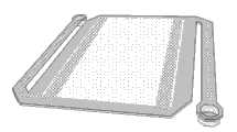
图2是传统的上下两个桥面之间只含一根连接柱、且连接柱与下桥面之间没有由金属构成的热量传输层的伞型双层微测辐射热计微桥的结构示意图:图中,(a) 该双层微桥的立体图,(b) 该双层微桥的上桥面的平面图,(c) 该双层微桥的下桥面的平面图,(d) 该双层微桥的截面图;Figure 2 shows the structure of the traditional umbrella-type double-layer microbolometer microbridge with only one connecting column between the upper and lower bridge decks and no heat transfer layer made of metal between the connecting column and the lower bridge deck Schematic diagram: among the figure, (a) the perspective view of the double-layer microbridge, (b) the plane view of the upper deck of the double-layer microbridge, (c) the plane view of the lower bridge deck of the double-layer microbridge, (d) the Cross-sectional view of the double-layer microbridge;
图3是本发明提出的上下两个桥面之间含有两根连接柱、且连接柱与下桥面之间含有一层由金属构成的热量传输层的双层微测辐射热计微桥的结构示意图:图中,(a) 该双层微桥的立体图,(b) 该双层微桥的上桥面的平面图,(c) 该双层微桥的下桥面的平面图,(d) 该双层微桥的截面图;Fig. 3 is the double-layer microbolometer microbridge that contains two connecting columns between the upper and lower bridge decks proposed by the present invention, and contains a heat transfer layer made of metal between the connecting columns and the lower bridge deck. Schematic diagram of the structure: among the figures, (a) the perspective view of the double-layer microbridge, (b) the plan view of the upper deck of the double-layer microbridge, (c) the plan view of the lower deck of the double-layer microbridge, (d) A cross-sectional view of the double-layer microbridge;
图4是不同的微测辐射热计微桥的光吸收率随波长变化的仿真结果。其中,1L、2L分别表示传统的I型单层微桥、和本发明提出的双层微桥的结果;Fig. 4 is the simulation result of the light absorption rate of different microbolometer microbridges as a function of wavelength. Wherein, 1L, 2L respectively represent the result of the traditional I-type single-layer microbridge and the double-layer microbridge proposed by the present invention;
图5 在相同的强度为20 W/m2的辐射量作用下,不同双层微桥下桥面的温度分布的仿真结果:图中,(a) 传统的具有单根连接柱、且连接柱与下桥面之间没有由金属构成的伞型双层微桥,(b) 本发明提出的具有两根连接柱、且连接柱与下桥面之间含有一层由金属构成的热量传输层的双层微桥;Figure 5 Under the same radiation intensity of 20 W/m2 , the simulation results of the temperature distribution of the bridge deck under different double-layer microbridges: in the figure, (a) the traditional one with a single connecting column and the connecting column There is no umbrella-shaped double-layer micro-bridge made of metal between the lower bridge deck, (b) the present invention has two connecting columns, and there is a heat transfer layer made of metal between the connecting columns and the lower bridge deck double-layer microbridge;
图6在相同的强度为+100 MPa的残余应力作用下,不同微桥的形变仿真结果:图中,(a) 传统的I型单层微桥,(b) 传统的S型双层微桥,(c) 传统的含单根连接柱、且连接柱与下桥面之间没有由金属构成的热量传输层的伞型双层微桥,(d) 本发明提出的含两根连接柱、且连接柱与下桥面之间含有一层由金属构成的热量传输层的双层微桥。Fig. 6 Under the same residual stress of +100 MPa, the deformation simulation results of different microbridges: in the figure, (a) the traditional I-type single-layer microbridge, (b) the traditional S-type double-layer microbridge , (c) the traditional umbrella-type double-layer micro-bridge containing a single connecting column, and there is no heat transfer layer made of metal between the connecting column and the lower bridge deck, (d) the proposed invention contains two connecting columns, In addition, there is a double-layer micro-bridge with a heat transfer layer made of metal between the connecting column and the lower bridge deck.
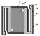
其中,1、硅衬底,2、二氧化硅钝化层,3、金属铝反射层,410、第一层聚酰亚胺薄膜,420、第二层聚酰亚胺薄膜,510、下桥面的第一层氮化硅膜,520、金属电极,530、热敏电阻薄膜,540、下桥面的第二层氮化硅膜,550、金属热量传输层, 6、微桥下桥面,610、微桥下桥面桥腿,620、微桥桥墩,630、下层光学谐振腔,7、微桥上桥面,710、上下桥面连接柱孔,720、上桥面氮化硅层,730、上下桥面连接柱,740、上桥面的金属光吸收增强材料,750、上层光学谐振腔, 8、悬浮的双层微桥,9、双层微测辐射热计。Among them, 1. silicon substrate, 2. silicon dioxide passivation layer, 3. metal aluminum reflective layer, 410, the first layer of polyimide film, 420, the second layer of polyimide film, 510, the lower bridge The first layer of silicon nitride film on the surface, 520, metal electrode, 530, thermistor film, 540, the second layer of silicon nitride film on the lower bridge surface, 550, metal heat transfer layer, 6, the lower bridge surface of the micro bridge , 610, legs of the lower deck of the micro-bridge, 620, pier of the micro-bridge, 630, optical resonant cavity in the lower layer, 7, upper deck of the micro-bridge, 710, connecting column holes of the upper and lower decks, 720, silicon nitride layer of the upper deck , 730, the upper and lower bridge deck connecting columns, 740, the metal light absorption enhancing material on the upper bridge deck, 750, the upper optical resonant cavity, 8, the suspended double-layer micro-bridge, 9, the double-layer microbolometer.
具体实施方式Detailed ways
下面将结合附图及具体实施方式对本发明作进一步的描述。The present invention will be further described below in conjunction with the accompanying drawings and specific embodiments.
采用本发明所提供的含上下两个独立桥面、两个桥面之间通过两根连接柱相连接、且下桥面含有一层由金属构成的热量传输层的双层微桥制作太赫兹探测器或红外探测器的微测辐射热计,具有更好的光学、热学及力学性能,能够提高器件的综合性能。The terahertz bridge is produced by using the double-layer microbridge provided by the present invention, which contains two independent upper and lower bridge decks, the two bridge decks are connected by two connecting columns, and the lower bridge deck contains a heat transfer layer made of metal. The microbolometer of the detector or infrared detector has better optical, thermal and mechanical properties, and can improve the comprehensive performance of the device.
实施例Example
本发明的制作步骤:(1)选用含有集成电路(ROIC)的硅晶圆片作为衬底1,清洗后用氮气吹干后,放入等离子体增强(PECVD)系统中,沉积一层非晶二氧化硅膜作为钝化层2,二氧化硅钝化层的厚度为100~2500 nm;(2)在二氧化硅钝化层的表面,利用磁控溅射系统,沉积一层厚度为50~1000 nm的金属铝,作为微桥8的反射层3;(3)在金属铝反射层3的表面光刻出悬浮微桥8的桥墩620的图形,刻蚀该金属铝反应层3至下面的二氧化硅钝化层2,形成微桥桥墩孔和金属铝孤岛;(4)在上述金属铝反应层3的表面,旋涂第一层厚度为1—10μm的光敏聚酰亚胺薄膜410;(5)对第一层聚酰亚胺薄膜410进行光刻处理,形成聚酰亚胺薄膜孤岛和悬浮微桥的桥墩孔;(6)在聚酰亚胺薄膜孤岛和桥墩孔的表面,利用PECVD在300oC下,沉积厚度为10~1500 nm的微桥下桥面6的第一层非晶氮化硅510,作为悬浮微桥8的支撑与绝缘材料;(7)利用反应器,在非晶氮化硅支撑膜的表面,沉积一层厚度为10~1000 nm的金属铝,图形化,作为器件的电极520;(8)对电极进行反溅之后,利用反应器制备一层厚度为5~2000nm的氧化钒薄膜530,作为微测辐射热计的热敏电阻材料和光吸收材料;(9)利用反应器,在金属电极520、以及热敏电阻薄膜530的表面,沉积微桥下桥面6的第二层非晶氮化硅膜540,厚度为10~1500 nm,作为电极520和敏感薄膜530的钝化层、以及微桥8应力的调控层;(10)利用反应器沉积微桥下桥面6的第二层金属550,厚度为10~1000 nm,图形化,作为热量的传输层;(11)在上述复合薄膜的表面光刻出悬浮微桥下桥面的结构图形,刻蚀该复合薄膜层至第一层聚酰亚胺层,形成悬浮微桥的下桥面6、桥腿610和桥墩620图形;(12)在下桥面由金属构成的热量传输层的表面,旋涂微桥的第二层厚度为1—10μm的光敏聚酰亚胺薄膜420;(13)对第二层聚酰亚胺薄膜420进行光刻处理,形成聚酰亚胺薄膜孤岛和上下桥面两个连接柱孔710;(14)在第二层聚酰亚胺薄膜孤岛的表面和上下桥面的两个连接柱孔710中,利用反应器沉积微桥的第三层非晶氮化硅膜720,厚度为10~1500 nm,作为微桥的上桥面光吸收材料及上下桥面之间的连接柱730;(15)在上述氮化硅膜720的表面,利用反应器沉积微桥上桥面的厚度为10~500 nm的金属钛740,作为光吸收增强材料;(16)在上述复合膜的表面光刻出悬浮双层微桥上桥面结构7图形,刻蚀该复合薄膜层至第二层聚酰亚胺层,形成悬浮微桥8的上桥面7图形;(17)采用氧等离子体去除上下两个桥面(7、6)、以及桥腿610图形下方的第一层410及第二层420聚酰亚胺薄膜,形成独立的上下两个空腔(750、630),作为器件的光学谐振腔。由此制备双层微测辐射热计9。The manufacturing steps of the present invention: (1) select a silicon wafer containing an integrated circuit (ROIC) as the substrate 1, clean it and dry it with nitrogen, put it into a plasma enhanced (PECVD) system, and deposit a layer of amorphous The silicon dioxide film is used as the
如图3所示,本发明提出的上下两个桥面之间含有两根连接柱、下桥面含有一层由金属构成的热量传输层的双层非制冷微测辐射热计微桥结构。作为对比,图1及2分别展示传统的单层I型微桥、以及传统的上下两个桥面之间只有单根连接柱、且连接柱与下桥面之间没有由金属构成的热量传输层的伞型双层微桥结构。As shown in FIG. 3 , the present invention proposes a double-layer uncooled microbolometer microbridge structure with two connecting columns between the upper and lower bridge decks and a heat transfer layer made of metal on the lower deck. For comparison, Figures 1 and 2 show the traditional single-layer I-type microbridge, and the traditional upper and lower bridge decks with only a single connecting column, and there is no heat transfer between the connecting column and the lower bridge deck made of metal Layered umbrella-type double-layer microbridge structure.
作为优选:本发明提出的双层微测辐射热计微桥下桥面的支撑层和钝化层、以及上桥面的光吸收层,除了氮化硅(SiNx)薄膜,还可以是非晶硅(a-Si)膜、其它厚度及组分的氧化硅(SiOx)膜、氮氧化硅(SiNxOy)膜,或者是业内所知的氧化铝(AlOx)膜、氧化铪(HfOx)膜、氧化铝铪(HfAlOx)膜等其中的一种、以及它们的复合膜。As a preference: the supporting layer and passivation layer of thelower deck of the double-layer microbolometer microbridge proposed by the present invention, and the light absorption layer of the upper bridge deck can also be amorphous Silicon (a-Si) film, silicon oxide (SiOx ) film of other thickness and composition, silicon oxynitride (SiNx Oy ) film, or aluminum oxide (AlOx ) film known in the industry, hafnium oxide ( One of HfOx ) film, hafnium aluminum oxide (HfAlOx ) film, and a composite film thereof.
作为优选:本发明提出的微桥电极及热量传输层,可以是金属Al、或金属Au、Ti、TiNx、TiSix、TiWx、W、WSix、Ni、NiSix、Ta、TaNx、Fe、Pt、Cu、Ag、NiCr合金当中的一种或几种的混合物。As preference: the microbridge electrode and the heat transfer layer proposed by the present invention can be metal Al, or metal Au, Ti,TiNx ,TiSix ,TiWx , W,WSix , Ni,NiSix , Ta,TaNx , One or a mixture of Fe, Pt, Cu, Ag, NiCr alloys.
作为优选:本发明的热敏电阻材料,可以是氧化钒薄膜、或氧化钛薄膜、非晶硅薄膜、氧化钒复合膜、氧化钛复合薄膜、非晶硅复合膜当中的一种。本发明提出的微桥下桥面的桥腿的形状也不受特别限制,可以是I型、L型、S型、或业内所知的其它悬浮微桥形状当中的一种。Preferably: the thermistor material of the present invention can be one of vanadium oxide film, titanium oxide film, amorphous silicon film, vanadium oxide composite film, titanium oxide composite film, and amorphous silicon composite film. The shape of the legs of the bridge deck under the micro-bridge proposed by the present invention is not particularly limited, and can be I-shaped, L-shaped, S-shaped, or one of other suspended micro-bridge shapes known in the industry.
图4表明,在3~14μm波段,传统的单层微桥(图1)的光吸收率仅为0.50~0.58(图4a)。但是在相同波段,本发明提出的双层微桥(图3)的光吸收率高达0.78~0.88(图4b),明显优于传统的单层微桥(图1)。所以,将单层微桥改为本发明所提出的双层微桥(图3),红外探测器的光学性能得到明显提升(光吸收率增大34~76%),其原因是该双层微桥结构(图3)包含上下两个光学谐振腔,有利于增强光子的吸收,而且,双层微桥下桥面中的氮化硅层还能继续吸收穿透过上桥面的氮化硅层的红外辐射。此外,图3所示的本发明提出的双层微桥的填充因子较高(> 90%),明显优于图1所示的传统的单层微桥(50~60 %)。Figure 4 shows that in the 3-14 μm band, the light absorption rate of the traditional single-layer microbridge (Figure 1) is only 0.50-0.58 (Figure 4a). However, in the same wavelength band, the light absorption rate of the double-layer microbridge proposed by the present invention (Fig. 3) is as high as 0.78~0.88 (Fig. 4b), which is obviously better than the traditional single-layer microbridge (Fig. 1). Therefore, changing the single-layer microbridge to the double-layer microbridge proposed by the present invention (Figure 3), the optical performance of the infrared detector is significantly improved (the light absorption rate increases by 34~76%), the reason is that the double-layer The microbridge structure (Fig. 3) contains two optical resonant cavities, which are conducive to enhancing the absorption of photons. Moreover, the silicon nitride layer in the lower bridge surface of the double-layer microbridge can continue to absorb the nitride oxide penetrating through the upper bridge surface. Infrared radiation from a silicon layer. In addition, the filling factor of the double-layer microbridge proposed by the present invention shown in FIG. 3 is relatively high (> 90%), which is obviously better than that of the traditional single-layer microbridge (50~60%) shown in FIG. 1 .
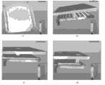
图5为在相同强度的辐射量(20 W/m2)的作用下,假设入射光完全被微桥所吸收时,不同双层微桥下桥面的温度分布的仿真结果。对于现有的上下两个桥面之间仅含单根连接柱、且连接柱与下桥面之间没有由金属构成的热传输层的伞型双层微桥(图2),在热敏电阻材料所处的下桥面6中,温度的变化范围宽达48.1~57.7 mk,
图6结果表明,在相同的强度为+100 PMa的残余应力作用下,传统单层I型微桥(图1)的形变最大值为0.03013μm图6a)。当相同的残余应力作用在现有的S型双层微桥中时,这种双层微桥形变的最大值高达0.05124 μm(图6b),远远高于单层I型(图6a)。形变值越大,微桥结构的稳定性越差。所以,S型双层微桥的稳定性较差。相同条件下,现有的上下两个桥面之间含单根连接柱、且连接柱与下桥面之间没有由金属构成的热传输层的伞型双层微桥(图2)的形变最大值为0.02959μm(图6c),与单层I型(图1)相当,优于S型双层微桥。如果采用图3所示的本发明提出的上下两个桥面之间含有两根连接柱、且连接柱与下桥面之间含有一层由金属构成的热量传输层的双层微桥结构,其形变最大值为0.03454μm(图6d),与传统的单层(图6a)及现有的伞型双层微桥(图6c)的形变值相当,远低于现有的S型双层微桥的形变值(图6b),说明本发明提出的双层微桥(图3)的力学稳定性优良。The results in Fig. 6 show that under the same residual stress with an intensity of +100 PMa, the deformation maximum of the traditional single-layer type I microbridge (Fig. 1) is 0.03013 μm (Fig. 6a). When the same residual stress acts on the existing S-type double-layer microbridge, the maximum deformation of this double-layer microbridge is as high as 0.05124μm (Fig. 6b), much higher than monolayer type I (Fig. 6a). The larger the deformation value, the worse the stability of the microbridge structure. Therefore, the stability of the S-type double-layer microbridge is poor. Under the same conditions, the deformation of the existing umbrella-shaped double-layer microbridge (Fig. The maximum value is 0.02959 μm (Fig. 6c), which is comparable to the single-layer type I (Fig. 1) and better than the S-type double-layer microbridge. If the present invention shown in Fig. 3 contains two connecting columns between the upper and lower bridge decks, and a double-layer microbridge structure with a heat transfer layer made of metal between the connecting columns and the lower bridge deck, Its maximum deformation value is 0.03454 μm (Figure 6d), which is comparable to the deformation value of the traditional single layer (Figure 6a) and the existing umbrella-shaped double-layer microbridge (Figure 6c), much lower than the existing S-shaped double-layer microbridge. The deformation value of the microbridge (Fig. 6b) shows that the mechanical stability of the double-layer microbridge proposed by the present invention (Fig. 3) is excellent.
经以上分析,本发明提出一种采用含上下两个独立桥面(7、6)、且上下两个桥面之间通过两根连接柱730相连接、下桥面中含有由金属构成的热量传输层550的特殊的双层微桥8(图3)制作的太赫兹探测器或红外探测器微测辐射热计(9),能够提高微测辐射热计的光学(光吸收率增大)、热学(温度均匀性更好)等性能,获得更优的综合性能,符合太赫兹探测器或红外探测器的需要。并且本发明提出的双层微桥8(图3)只是在传统单层I型微桥(图1)的基础上添加一些后续的旋涂、光刻、镀膜等传统工艺,技术难度不大、有利于器件的大规模制造。Based on the above analysis, the present invention proposes a bridge with upper and lower independent bridge decks (7, 6), and the upper and lower bridge decks are connected by two connecting
Claims (10)
Priority Applications (1)
| Application Number | Priority Date | Filing Date | Title |
|---|---|---|---|
| CN 201110299176CN102393252B (en) | 2011-09-29 | 2011-09-29 | Two-layer micrometering bolometer and manufacturing method thereof |
Applications Claiming Priority (1)
| Application Number | Priority Date | Filing Date | Title |
|---|---|---|---|
| CN 201110299176CN102393252B (en) | 2011-09-29 | 2011-09-29 | Two-layer micrometering bolometer and manufacturing method thereof |
Publications (2)
| Publication Number | Publication Date |
|---|---|
| CN102393252Atrue CN102393252A (en) | 2012-03-28 |
| CN102393252B CN102393252B (en) | 2013-01-16 |
Family
ID=45860611
Family Applications (1)
| Application Number | Title | Priority Date | Filing Date |
|---|---|---|---|
| CN 201110299176Expired - Fee RelatedCN102393252B (en) | 2011-09-29 | 2011-09-29 | Two-layer micrometering bolometer and manufacturing method thereof |
Country Status (1)
| Country | Link |
|---|---|
| CN (1) | CN102393252B (en) |
Cited By (12)
| Publication number | Priority date | Publication date | Assignee | Title |
|---|---|---|---|---|
| CN105712284A (en)* | 2014-12-02 | 2016-06-29 | 无锡华润上华半导体有限公司 | Fabrication method of MEMS (Micro Electro Mechanical Systems) double layer suspended micro structure and MEMS infrared detector |
| CN106115604A (en)* | 2016-07-25 | 2016-11-16 | 电子科技大学 | Terahertz micro-metering bolometer based on metamaterial structure and preparation method thereof |
| CN106129167A (en)* | 2016-07-20 | 2016-11-16 | 电子科技大学 | A kind of graphene terahertz detector and preparation method thereof |
| CN106935677A (en)* | 2015-12-31 | 2017-07-07 | 上海丽恒光微电子科技有限公司 | A kind of Infrared Detectors and preparation method thereof |
| CN106935676A (en)* | 2015-12-31 | 2017-07-07 | 上海丽恒光微电子科技有限公司 | A kind of Infrared Detectors and preparation method thereof |
| CN107068780A (en)* | 2017-04-18 | 2017-08-18 | 烟台睿创微纳技术股份有限公司 | Method for oxidation prepares infrared detector of titanium oxide heat-sensitive layer and preparation method thereof |
| CN107063472A (en)* | 2017-04-18 | 2017-08-18 | 烟台睿创微纳技术股份有限公司 | Method for oxidation prepares curved surface focus planar detector of heat-sensitive layer and preparation method thereof |
| CN109596225A (en)* | 2018-12-20 | 2019-04-09 | 西安工业大学 | A kind of infrared detector and preparation method thereof with high-effect resonant cavity |
| CN109946261A (en)* | 2017-12-20 | 2019-06-28 | 中国科学院深圳先进技术研究院 | Terahertz wave detection device with adjustable absorption wavelength and preparation method thereof |
| CN110044494A (en)* | 2019-03-22 | 2019-07-23 | 清华大学 | A kind of heat-sensitive eye array and its manufacturing method |
| CN113447142A (en)* | 2021-06-25 | 2021-09-28 | 北京北方高业科技有限公司 | Reinforced CMOS infrared detector |
| US11656128B2 (en) | 2021-08-06 | 2023-05-23 | Industrial Technology Research Institute | Microelectromechanical infrared sensing device and fabrication method thereof |
Citations (2)
| Publication number | Priority date | Publication date | Assignee | Title |
|---|---|---|---|---|
| US6307194B1 (en)* | 1999-06-07 | 2001-10-23 | The Boeing Company | Pixel structure having a bolometer with spaced apart absorber and transducer layers and an associated fabrication method |
| CN101881667A (en)* | 2010-06-24 | 2010-11-10 | 电子科技大学 | A kind of unrefrigerated microbolometer and preparation method thereof |
- 2011
- 2011-09-29CNCN 201110299176patent/CN102393252B/ennot_activeExpired - Fee Related
Patent Citations (2)
| Publication number | Priority date | Publication date | Assignee | Title |
|---|---|---|---|---|
| US6307194B1 (en)* | 1999-06-07 | 2001-10-23 | The Boeing Company | Pixel structure having a bolometer with spaced apart absorber and transducer layers and an associated fabrication method |
| CN101881667A (en)* | 2010-06-24 | 2010-11-10 | 电子科技大学 | A kind of unrefrigerated microbolometer and preparation method thereof |
Cited By (18)
| Publication number | Priority date | Publication date | Assignee | Title |
|---|---|---|---|---|
| CN105712284A (en)* | 2014-12-02 | 2016-06-29 | 无锡华润上华半导体有限公司 | Fabrication method of MEMS (Micro Electro Mechanical Systems) double layer suspended micro structure and MEMS infrared detector |
| US10301175B2 (en) | 2014-12-02 | 2019-05-28 | Csmc Technologies Fab1 Co., Ltd | Method for manufacturing MEMS double-layer suspension microstructure, and MEMS infrared detector |
| CN105712284B (en)* | 2014-12-02 | 2017-09-29 | 无锡华润上华半导体有限公司 | The preparation method and MEMS infrared detectors of MEMS Double-layered suspended micro-structurals |
| CN106935676A (en)* | 2015-12-31 | 2017-07-07 | 上海丽恒光微电子科技有限公司 | A kind of Infrared Detectors and preparation method thereof |
| CN106935677A (en)* | 2015-12-31 | 2017-07-07 | 上海丽恒光微电子科技有限公司 | A kind of Infrared Detectors and preparation method thereof |
| CN106935676B (en)* | 2015-12-31 | 2019-03-26 | 上海丽恒光微电子科技有限公司 | A kind of infrared detector and preparation method thereof |
| CN106935677B (en)* | 2015-12-31 | 2018-12-11 | 上海丽恒光微电子科技有限公司 | A kind of infrared detector and preparation method thereof |
| CN106129167A (en)* | 2016-07-20 | 2016-11-16 | 电子科技大学 | A kind of graphene terahertz detector and preparation method thereof |
| CN106115604B (en)* | 2016-07-25 | 2018-09-28 | 电子科技大学 | Terahertz micro-metering bolometer based on metamaterial structure and preparation method thereof |
| CN106115604A (en)* | 2016-07-25 | 2016-11-16 | 电子科技大学 | Terahertz micro-metering bolometer based on metamaterial structure and preparation method thereof |
| CN107063472A (en)* | 2017-04-18 | 2017-08-18 | 烟台睿创微纳技术股份有限公司 | Method for oxidation prepares curved surface focus planar detector of heat-sensitive layer and preparation method thereof |
| CN107068780A (en)* | 2017-04-18 | 2017-08-18 | 烟台睿创微纳技术股份有限公司 | Method for oxidation prepares infrared detector of titanium oxide heat-sensitive layer and preparation method thereof |
| CN109946261A (en)* | 2017-12-20 | 2019-06-28 | 中国科学院深圳先进技术研究院 | Terahertz wave detection device with adjustable absorption wavelength and preparation method thereof |
| CN109946261B (en)* | 2017-12-20 | 2021-07-16 | 中国科学院深圳先进技术研究院 | Terahertz wave detection device with adjustable absorption wavelength and preparation method thereof |
| CN109596225A (en)* | 2018-12-20 | 2019-04-09 | 西安工业大学 | A kind of infrared detector and preparation method thereof with high-effect resonant cavity |
| CN110044494A (en)* | 2019-03-22 | 2019-07-23 | 清华大学 | A kind of heat-sensitive eye array and its manufacturing method |
| CN113447142A (en)* | 2021-06-25 | 2021-09-28 | 北京北方高业科技有限公司 | Reinforced CMOS infrared detector |
| US11656128B2 (en) | 2021-08-06 | 2023-05-23 | Industrial Technology Research Institute | Microelectromechanical infrared sensing device and fabrication method thereof |
Also Published As
| Publication number | Publication date |
|---|---|
| CN102393252B (en) | 2013-01-16 |
Similar Documents
| Publication | Publication Date | Title |
|---|---|---|
| CN102393252B (en) | Two-layer micrometering bolometer and manufacturing method thereof | |
| CN102393251B (en) | Two-layer micrometering bolometer and manufacturing method thereof | |
| CN106352989B (en) | A kind of production method and structure of non-refrigerated infrared focal plane probe microbridge | |
| CN102426060B (en) | Terahertz or infrared micro-bolometer and manufacturing method thereof | |
| TW536621B (en) | Advanced high speed, multi-level uncooled bolometer and method for fabricating same | |
| CN102384789B (en) | Infrared focal plane array device and manufacturing method thereof | |
| WO2012071820A1 (en) | Infrared detector and method of manufacture thereof and multi-band uncooled infrared focal plane | |
| CN109813448B (en) | Bispectral metasurface integrated uncooled infrared detector and fabrication method | |
| CN104535198A (en) | Terahertz microbolometer based on metamaterial absorber and preparation method of terahertz microbolometer | |
| CN106784165B (en) | A kind of novel double-layer non-refrigerated infrared focal plane probe dot structure and preparation method thereof | |
| CN202329818U (en) | Uncooled infrared detection device | |
| CN102226719A (en) | Infrared Absorbing Structure and Uncooled Infrared Detector Based on the Structure | |
| EP3522217B1 (en) | Method to prepare pixel for uncooled infrared focal plane detector | |
| CN103940518B (en) | A low thermal conductivity terahertz detection unit microbridge structure and its preparation method | |
| JP2012194080A (en) | Bolometer type thz wave detector | |
| JP2006226890A (en) | Thermal infrared detection element | |
| CN108333653B (en) | Electromagnetic wave absorber based on refractory material | |
| CN110118604B (en) | Wide-spectrum microbolometer based on mixed resonance mode and preparation method thereof | |
| CN106052883A (en) | Three-layer micro-bridge structure, three-layer uncooled micro-bolometer and preparation method thereof | |
| JP5760297B2 (en) | Thermal infrared sensor and method for manufacturing thermal infrared sensor | |
| CN106124066A (en) | The microbolometer of a kind of high fill factor and preparation method | |
| CN106092334A (en) | A kind of Infrared Detectors based on carbon nanometer infrared absorption layer | |
| CN109813446A (en) | A kind of composite absorption film layer uncooled infrared focal plane and manufacturing method | |
| CN108358157B (en) | Metamaterial microbridge structure and preparation method thereof | |
| CN102185025A (en) | Manufacturing process of metal waveguide microcavity optical coupling structure used for photoelectric functional devices |
Legal Events
| Date | Code | Title | Description |
|---|---|---|---|
| C06 | Publication | ||
| PB01 | Publication | ||
| C10 | Entry into substantive examination | ||
| SE01 | Entry into force of request for substantive examination | ||
| C14 | Grant of patent or utility model | ||
| GR01 | Patent grant | ||
| CF01 | Termination of patent right due to non-payment of annual fee | ||
| CF01 | Termination of patent right due to non-payment of annual fee | Granted publication date:20130116 Termination date:20180929 |