CN102386507A - Ground shield for an electrical connector - Google Patents
Ground shield for an electrical connectorDownload PDFInfo
- Publication number
- CN102386507A CN102386507ACN2011102537008ACN201110253700ACN102386507ACN 102386507 ACN102386507 ACN 102386507ACN 2011102537008 ACN2011102537008 ACN 2011102537008ACN 201110253700 ACN201110253700 ACN 201110253700ACN 102386507 ACN102386507 ACN 102386507A
- Authority
- CN
- China
- Prior art keywords
- ground
- electrical
- contact
- shield
- mating
- Prior art date
- Legal status (The legal status is an assumption and is not a legal conclusion. Google has not performed a legal analysis and makes no representation as to the accuracy of the status listed.)
- Granted
Links
Images


Classifications
- H—ELECTRICITY
- H01—ELECTRIC ELEMENTS
- H01R—ELECTRICALLY-CONDUCTIVE CONNECTIONS; STRUCTURAL ASSOCIATIONS OF A PLURALITY OF MUTUALLY-INSULATED ELECTRICAL CONNECTING ELEMENTS; COUPLING DEVICES; CURRENT COLLECTORS
- H01R13/00—Details of coupling devices of the kinds covered by groups H01R12/70 or H01R24/00 - H01R33/00
- H01R13/66—Structural association with built-in electrical component
- H01R13/6608—Structural association with built-in electrical component with built-in single component
- H01R13/6625—Structural association with built-in electrical component with built-in single component with capacitive component
- H—ELECTRICITY
- H01—ELECTRIC ELEMENTS
- H01R—ELECTRICALLY-CONDUCTIVE CONNECTIONS; STRUCTURAL ASSOCIATIONS OF A PLURALITY OF MUTUALLY-INSULATED ELECTRICAL CONNECTING ELEMENTS; COUPLING DEVICES; CURRENT COLLECTORS
- H01R13/00—Details of coupling devices of the kinds covered by groups H01R12/70 or H01R24/00 - H01R33/00
- H01R13/648—Protective earth or shield arrangements on coupling devices, e.g. anti-static shielding
- H01R13/658—High frequency shielding arrangements, e.g. against EMI [Electro-Magnetic Interference] or EMP [Electro-Magnetic Pulse]
- H01R13/6581—Shield structure
- H01R13/6585—Shielding material individually surrounding or interposed between mutually spaced contacts
- H01R13/6586—Shielding material individually surrounding or interposed between mutually spaced contacts for separating multiple connector modules
- H01R13/6587—Shielding material individually surrounding or interposed between mutually spaced contacts for separating multiple connector modules for mounting on PCBs
Landscapes
- Details Of Connecting Devices For Male And Female Coupling (AREA)
Abstract
Translated fromChinese
Description
Translated fromChinese技术领域technical field
本发明涉及具有电接地路径的电连接器。The present invention relates to electrical connectors having an electrical ground path.
背景技术Background technique
两个或多个电气部件经常电连接在一起以可操作地连接电气部件。特别地,在电气部件内相应的信号路径电连接在一起,例如使用中间触头和/或中间电连接器的导体,以在电气部件之间建立信号路径。相似地,在电气部件内相应的电接地路径和/或平面电连接在一起以在电气部件之间提供一个或多个电接地路径。互连电气部件的一种具体的例子包括互连两个印刷电路(有时称为“电路板”或“印刷电路板”)。印刷电路之一有时包括具有输出的驱动电路,其驱动其它印刷电路的接收电路的输入。Two or more electrical components are often electrically connected together to operatively connect the electrical components. In particular, corresponding signal paths within the electrical components are electrically connected together, for example using intermediate contacts and/or intermediate electrical connector conductors, to establish signal paths between the electrical components. Similarly, corresponding electrical ground paths and/or planes within electrical components are electrically connected together to provide one or more electrical ground paths between electrical components. A specific example of interconnecting electrical components includes interconnecting two printed circuits (sometimes referred to as "circuit boards" or "printed circuit boards"). One of the printed circuits sometimes includes a driver circuit with an output that drives the input of the receiving circuit of the other printed circuit.
电连接在一起的电气部件可以经受在其之间的不经意的直流(DC)耦合。特别地,DC可在电气部件之间不经意地传输。例如,在印刷电路上的互连的驱动和接收电路可以不经意地DC耦合。在互连的电气部件之间的不经意的DC耦合对于在其之间传输高速(例如,大致1千兆比特每秒(Gbps)以上)差分信号的电气部件来说可能是特别麻烦。Electrical components that are electrically connected together can experience inadvertent direct current (DC) coupling between them. In particular, DC can be inadvertently transferred between electrical components. For example, interconnected drive and receive circuits on printed circuits can be inadvertently DC coupled. Inadvertent DC coupling between interconnected electrical components can be particularly troublesome for electrical components between which high speed (eg, above approximately 1 gigabit per second (Gbps)) differential signals are transmitted.
为了阻挡电气部件之间的DC耦合,通常沿着电气部件的一个或两个的信号路径提供分立的电容器。但是,在电气部件上或附近仅仅有限数量的空间是可用的。例如,由于更小的电子封装和更高的信号传输速度的需求的增长,印刷电路和其它电气部件可能对于传统的分立DC阻挡电容没有空间。增加分立电容至电气部件以阻挡不经意的的DC耦合可能因此增加电气部件的尺寸。除了或替换增加的尺寸之外,将分立电容增加至电气部件会减小电气部件的触头、导体、电路和/或类似的部件的密度,这会不利的影响电气部件之间的信号传输速率。另外,在电气部件内的分立电容的寄生电感、电容、电阻和/或类似特性也可能减少在电气部件之间传输高速差分信号的电气部件之间的信号传输速度。To block DC coupling between electrical components, discrete capacitors are often provided along the signal paths of one or both of the electrical components. However, only a limited amount of space is available on or near the electrical components. For example, printed circuits and other electrical components may not have room for traditional discrete DC blocking capacitors due to the growing demand for smaller electronic packages and higher signal transmission speeds. Adding discrete capacitors to electrical components to block inadvertent DC coupling may thus increase the size of the electrical components. In addition to or instead of increased size, adding discrete capacitance to an electrical component reduces the density of contacts, conductors, circuits, and/or the like of the electrical component, which can adversely affect the rate of signal transfer between the electrical components . Additionally, parasitic inductance, capacitance, resistance, and/or similar properties of discrete capacitors within electrical components may also reduce signal transmission speeds between electrical components that transmit high speed differential signals between the electrical components.
需要一种能够阻挡电气部件之间的不经意的DC耦合而没有添加分立的电容至电气部件的装置。What is needed is a device that blocks inadvertent DC coupling between electrical components without adding discrete capacitance to the electrical components.
发明内容Contents of the invention
根据本发明,用于电连接器的触头模块包括具有配合边缘和安装边缘的模块主体。通过模块主体保持的引线框包括至少一个从配合触头延伸到安装触头的电引线。配合触头从模块主体的配合边缘向外延伸,安装触头从模块主体的安装边缘向外延伸。接地屏蔽安装在模块主体上。接地屏蔽包括屏蔽主体,该屏蔽主体具有彼此分开一间隙的两个导电板和位于该间隙内的电介质,其中该屏蔽主体的板和电介质限定了电容器。According to the invention, a contact module for an electrical connector comprises a module body having a mating edge and a mounting edge. A lead frame retained by the module body includes at least one electrical lead extending from the mating contact to the mounting contact. The mating contacts extend outwardly from the mating edge of the module body, and the mounting contacts extend outwardly from the mounting edge of the module body. The ground shield is mounted on the module body. The ground shield includes a shield body having two conductive plates separated from each other by a gap and a dielectric within the gap, wherein the plates and the dielectric of the shield body define a capacitor.
附图说明Description of drawings
图1是电气系统的示例性实施例的示意图;1 is a schematic diagram of an exemplary embodiment of an electrical system;
图2是连接器系统的示例性实施例的透视图,其示出在不配合位置的插座组件的示例性实施例和插头组件的示例性实施例;2 is a perspective view of an exemplary embodiment of a connector system showing an exemplary embodiment of a receptacle assembly and an exemplary embodiment of a plug assembly in an unmated position;
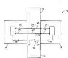
图3是图2示出的插座组件的触头模块的示例性实施例的部分的分解透视图;3 is an exploded perspective view of portions of an exemplary embodiment of a contact module of the receptacle assembly shown in FIG. 2;
图4是图3示出的触头模块的接地屏蔽的示例性实施例的透视图;4 is a perspective view of an exemplary embodiment of a ground shield of the contact module shown in FIG. 3;
图5是图3示出的触头模块的接地屏蔽的示例性替代实施例的透视图;以及5 is a perspective view of an exemplary alternative embodiment of a ground shield of the contact module shown in FIG. 3; and
图6是电缆的示例性实施例的一部分的部分剖开的透视图。6 is a perspective view, partially cut away, of a portion of an exemplary embodiment of a cable.
具体实施方式Detailed ways
图1是电气系统10的示例性实施例的示意图。系统10包括两个电气部件12和14以及电连接器16。电连接器16在电气部件12和14之间提供电连接。特别地,电连接器16包括外壳18,其保持一个或多个信号导体20和一个或多个接地导体22。每个信号导体20电连接于电气部件12和14的各个电触头24和26。每个电触头24和26在各个电气部件12和14内限定了信号路径的至少一部分。电连接器16的每个信号导体20限定了电气部件12和14之间的信号路径28。特别地,每个信号导体20限定了从电气部件12的电触头24经过电连接器16的外壳18到达电气部件14的电触头26的信号路径28,和/或反之亦然。每个接地导体22分别电连接于每个电气部件12和14的电接地触头和/或平面30和32。每个接地触头和/或平面30和32在各个电气部件12和14内限定了电接地路径的至少一部分。电连接器16的每个接地导体22分别限定了在电气部件12和14的接地触头和/或平面30和32之间和经过外壳18的电接地路径34。FIG. 1 is a schematic diagram of an exemplary embodiment of an
根据本发明的实施例,电连接器16包括设置在电接地路径34内的电容器36。特别地,电容器36在接地导体22的任何位置上可操作地连接于电连接器16的接地导体22。电容器36被配置为减小或消除电气部件12和14之间的直流(DC)耦合。电容器36可以是具有各种整体结构的各类型型的电容器。电容器36的例子包括但不限于平板电容器、固定电容器、可变电容器、绞合电容器、微调电容器、电解电容器、印刷电路板电容器、集成电路电容器、真空电容器和/或类似电容器。According to an embodiment of the present invention,
在一些实施例中,电容器36至少部分被接地导体22限定。在其它实施例中,电容器36是嵌入并与接地导体22串联的电容性结构。电容性结构一般包括被至少一个介电层分开的至少两个导电层。如这里使用的,术语“可操作地连接到”是要包括其中电容器36的一个或多个导电层至少部分被接地导体22限定的实施例和其中电容器36的导电层是嵌入并与接地导体22串联的物理上分开的结构的实施例。尽管在图1中的电连接器16仅包括接地路径34内的单个电容器36,但是在电连接器16的接地路径34内的任何位置可设置任何数量的电容器36。In some embodiments,
在示例性实施例中,电连接器16包括被设置为传送差分对信号的两个信号导体20。除了或替换差分对信号导体20以外,电连接器16可包括没有设置为差分对的一个或多个信号导体20。电连接器16可包括任何数量的信号导体20,任何数量的信号导体20可以设置或不设置为差分对。尽管仅仅示出一个,但电连接器16可包括任何数量的接地导体22。In the exemplary embodiment,
每个电气部件12和14可是任何类型的电气部件,例如但不限于计算机、处理器、存储器、印刷电路、信号驱动器、信号接收器、电源、电负载、集成电路、视频装置和/或元件、音频装置和/或元件、通信装置和/或元件、手持装置、个人数字助理(PDA)、高速(例如至少1Gbps的数据速率)电气装置和/或类似装置。每个电气部件12和14在此可被称为“第一电气部件”和/或“第二电气部件”。Each
此处说明和/或描述的主题不限于任何特别类型的电连接器。而是,可以在将任意类型的电气部件互连在一起的任意类型的电连接器的接地路径内提供一个或多个电容器。例如电连接器16可以是但不限于,将两个印刷电路互连在一起的电连接器(例如以下参照图2-6描述的连接系统100)、收发装置、电插头和/或端口、两个或多个零件可分离的连接器的一半或全部、电缆和/或类似装置。The subject matter illustrated and/or described herein is not limited to any particular type of electrical connector. Rather, one or more capacitors may be provided within the ground path of any type of electrical connector that interconnects any type of electrical components together. For example,
图2是正交连接系统100的示例性实施例的透视图,其示出了两个可以直接配合在一起的连接器组件102和104。连接器组件102和104各自电连接于各个印刷电路106和108。连接器组件102和104用于沿着分离配合接口将印刷电路106和108彼此电连接。印刷电路106和108彼此正交,连接器组件102和104彼此正交。例如,连接器组件102和104相对彼此转向90°。配合轴110延伸穿过连接器组件102和104。连接器组件102和104沿着配合轴110且在与其平行的方向配合在一起。在示例性实施例中,印刷电路106和108两个都大致上平行于配合轴110延伸。2 is a perspective view of an exemplary embodiment of an orthogonal connection system 100 showing two connector assemblies 102 and 104 that may be mated directly together. The connector assemblies 102 and 104 are each electrically connected to a respective printed circuit 106 and 108 . Connector assemblies 102 and 104 are used to electrically connect printed circuits 106 and 108 to each other along a breakaway mating interface. Printed circuits 106 and 108 are orthogonal to each other, and connector assemblies 102 and 104 are orthogonal to each other. For example, connector assemblies 102 and 104 are turned 90° relative to each other. The mating shaft 110 extends through the connector assemblies 102 and 104 . The connector assemblies 102 and 104 are mated together along and in a direction parallel to the mating axis 110 . In the exemplary embodiment, printed circuits 106 and 108 both extend substantially parallel to mating axis 110 .
在示例性实施例中,连接器组件102构造成插头组件,下面把它称为“插头组件102”。连接器组件104构造成插座组件,下面把它称为“插座组件104”。插头组件102和插座组件104的每个在此都可被称为“电连接器”。In the exemplary embodiment, connector assembly 102 is configured as a header assembly, hereinafter referred to as "header assembly 102". The connector assembly 104 is configured as a receptacle assembly, hereinafter referred to as "receptacle assembly 104". Each of plug assembly 102 and receptacle assembly 104 may be referred to herein as an "electrical connector."
插头组件102包括外壳112,该外壳112在外壳112的端部116具有配合面114。多个触头模块118被外壳112保持。触头模块118电连接于印刷电路106。配合面114选择性地取向为大致垂直于印刷电路106和配合轴110。与插头组件102相似,插座组件104包括外壳122,该外壳122在外壳122的端部126具有配合面124。多个触头模块128通过外壳122保持。触头模块128电连接于印刷电路108。配合面124选择性地取向为大致垂直于印刷电路108和配合轴110。The header assembly 102 includes a housing 112 having a mating face 114 at an end 116 of the housing 112 . A plurality of contact modules 118 are held by the housing 112 . The contact module 118 is electrically connected to the printed circuit 106 . The mating face 114 is selectively oriented generally perpendicular to the printed circuit 106 and the mating axis 110 . Like the header assembly 102 , the receptacle assembly 104 includes a housing 122 having a mating face 124 at an end 126 of the housing 122 . A plurality of
插头组件102的外壳112包括腔132,其将插座组件104的外壳122的一部分接收于其中。配合触头134的阵列被配置在腔132之内以与插座组件104的相应的配合触头136(图3和4)相配合。当触头模块118被外壳112保持时,配合触头134从相应的触头模块118延伸到腔132中。配合触头134通过触头模块118的相应的电引线(未示出)电连接于印刷电路106。配合触头134包括信号触头134a和接地触头134b。Housing 112 of header assembly 102 includes a cavity 132 that receives a portion of housing 122 of receptacle assembly 104 therein. An array of mating contacts 134 is configured within cavity 132 to mate with corresponding mating contacts 136 ( FIGS. 3 and 4 ) of receptacle assembly 104 . When the contact modules 118 are retained by the housing 112 , the mating contacts 134 extend from the respective contact modules 118 into the cavities 132 . The mating contacts 134 are electrically connected to the printed circuit 106 through corresponding electrical leads (not shown) of the contact module 118 . The mating contacts 134 include signal contacts 134a and ground contacts 134b.
图3是插座组件104(图2)的触头模块128的示例性实施例的部分分解透视图。在示例性实施例中,触头模块128包括引线框148(虚线示出)、主体150、可选择的导电壳152、接地屏蔽154和配合触头136。配合触头136包括信号触头136a和接地触头136b。主体150此处可称为“模块主体”和/或“外壳”。信号触头136a此处可称为“信号导体”。接地触头136b此处可称为“接地导体”。FIG. 3 is a partially exploded perspective view of an exemplary embodiment of the
主体150保持引线框148和信号触头136a。壳152安装在主体150上以使得壳152至少部分围绕主体150。接地屏蔽154包括接地触头136b,并被安装在壳152上。由于接地屏蔽154安装在壳152上,壳152安装在主体150和接地屏蔽154之间的主体150上,则接地屏蔽154可被看作是间接地安装在主体150上。在一些替换实施例中,触头模块128并不包括壳152,且接地屏蔽154直接安装在主体150上。尽管示出为包括单个接地屏蔽154(安装在壳152的壳部分182a上),但触头模块128可替换地包括多于一个的接地屏蔽154。例如,触头模块128选择性地包括安装在壳152的壳部分182b上的其它接地屏蔽(未示出)。The
如下面所描述的,在示例性实施例中,接地屏蔽154包括电容器156,该电容器156由接地屏蔽154的主体196所限定。主体196具有向前配合边缘198和通常垂直于配合边缘198的底部安装边缘200。接地屏蔽主体196具有内侧206和外侧208。内侧206通常面对壳152,外侧208通常背离壳152。接地屏蔽154的主体196此处可称为“屏蔽主体”和/或“接地导体”。As described below, in the exemplary embodiment,
在示例性实施例中,接地屏蔽154包括接地触头136b,其从配合边缘198延伸。接地触头136b限定了接地屏蔽154的主体196的配合接口210。每个接地触头136b配置为与插头组件102(图2)的相应的接地触头134b(图2)配合。接地屏蔽154包括屏蔽尾部212,该屏蔽尾部212从安装边缘200延伸以电连接接地屏蔽154的主体196于印刷电路108(图2)。屏蔽尾部212限定了接地屏蔽154的主体196的安装接口214。In the exemplary embodiment,
接地屏蔽154提供穿过插座组件104(图2)的电接地路径,该电接地路径包括穿过插座组件104的外壳122(图2)和相应的触头模块128。特别地,穿过配合接口210和安装接口214之间的接地屏蔽154的主体196来限定该电接地路径。当插座组件104安装在印刷电路108上并与插头组件102配合时,接地屏蔽主体196限定了印刷电路106和108之间(图2)的一部分电接地路径。在印刷电路106和108之间的电接地路径的其它部分被设置为穿过插头组件102。The
图4是接地屏蔽154的示例性实施例的透视图。接地屏蔽154的主体196包括两个导电板216和218以及位于板216和218之间的电介层220。板216限定了接地屏蔽主体196的内侧206,板218限定了主体196的外侧208。最好如图3中所示,接地屏蔽154被安装在触头模块128的主体150上,使得板216在触头模块主体150的一侧174的至少一部分上延伸。再参照图4,选择地,板216之一包括接地触头136b,以及因此的配合接口210,同时其它板218包括屏蔽尾部212,以及因此的安装接口214,或反之亦然。可替换地,板216或218中的一个都包括接地触头136b和屏蔽尾部212,只要穿过主体196的电接地路径延伸穿过板216和218两者。板216和218的每个此处可被称为“第一板”、“第二板”和/或“导电层”。电介层220此处可被称为“电介质”。FIG. 4 is a perspective view of an exemplary embodiment of
接地屏蔽154的主体196的电介层220和板216和218限定了电容器156。特别地,板216和218彼此分开一间隙G。电介层220位于板216和218之间的间隙G内。换句话说,电介层220和板216和218与电介层220一起以层叠结构设置,该电介层220在板216和218之间延伸以分隔板216和218。空间分隔的板216和218以及电介层220从而限定了电容性结构。相应地,接地屏蔽154的主体196限定了电容器156。因为接地屏蔽154限定电接地路径的一部分,电容器156被设置在电接地路径内。Dielectric layer 220 and
可以选择电容器156的各种参数以提供预定的电容于接地屏蔽154的电接地路径内。选择地,电容器156用来有助于印刷电路106和108(图2)之间的DC耦合的减小和/或消除。可以选择电容器156的电容以在印刷电路106和108之间提供预定量的DC耦合的减小和/或消除。可以被选择以提供预定电容的电容器156的参数的例子包括,但不限于用于制造电介层220和板216和218的材料、板216和218的电导率、电介层220的电介常数、板216和218之间的距离(例如间隙G的数值)、板216和218的厚度、板216和218的表面积、板216和218彼此重叠的面积的量和/或类似参数。Various parameters of
板216和218的每个可由任何合适类型和结构的导电材料制造,例如但不限于,金属、金属性物质、非金属性导电材料、箔片、纸和/或类似物。电介层220可由任何合适类型和结构的电绝缘材料制造,例如但不限于,陶瓷、线绝缘材料、玻璃、纸、浸油纸、聚碳酸盐、聚酯、聚苯乙烯、聚丙稀、聚砜、聚四氟乙烯(PTFE;例如特氟龙

在示例性实施例中,板216和218被配置彼此大致平行,使得接地屏蔽154的主体196限定平行板电容器。替换地,板216和218被配置为彼此不平行。另外,尽管示出为大致平面,但板216和218的一些或全部表面可替换地是非平面的。除了平行板电容器之外,电容器156可是任何类型的具有任何类型的整体结构的电容器、任何材料和任何结构的电介质以及任何材料和任何结构的导体,不管电容器156是否通过接地屏蔽主体196限定或嵌入并与主体196串联电连接。除了平行板电容器,其他类型的电容器156的例子包括但不限于固定电容器、可变电容器、绞合电容器、微调电容器、电解电容器、印刷电路板电容器、集成电路电容器、真空电容器和/或类似类型。In the exemplary embodiment,
如上面所描述的,在示例性实施例中,接地屏蔽154的主体196限定电容器156。可替换地,电容器156是与接地屏蔽154的主体196物理分开的结构,其嵌入并与主体196串联电连接。例如,在一些可替换实施例中,接地屏蔽主体196仅仅包括板216或218中的一个,且电容器156嵌入并与单个板串联电连接。As described above, in the exemplary embodiment, the
在示例性实施例中,每个接地触头136b包括单个的横梁,该横梁被构造为与相应的接地触头134b(图2)的触片相配合。在可替换的实施例中,其它类型的触头可用于与接地触头134b的触片相配合或与插头组件102的其他类型的接地触头相配合。如此处示出的,屏蔽尾部212是安装在印刷电路108的通孔(未示出)中的针眼类型的触头。在可替换的实施例中,其它类型的触头可用于将接地屏蔽主体196电连接于印刷电路108,例如,但不限于,表面安装触头、焊接尾部和/或类似类型。In the exemplary embodiment, each
图5是接地屏蔽454的一个示例性的可替换的实施例的透视图。接地屏蔽454具有主体496,该主体496包括两个导电板516和518。板516和518彼此分开一间隙G1。一个或多个电介支架522在板516和518之间延伸以保持板516和518彼此分开一间隙G1。空气520在板516和518之间的间隙G1内延伸。分隔开的板516和518和在它们之间的间隙G1内延伸的空气520限定了电容性结构。相应地,接地屏蔽454的主体496限定电容器456。由于接地屏蔽454限定电接地路径的一部分,电容器456设置在电接地路径内。FIG. 5 is a perspective view of an exemplary alternative embodiment of
选择地,板516包括接地触头436b,而其它板518包括屏蔽尾部512,或者反之亦然。可替换地,板515或518之一都包括接地触头436b和屏蔽尾部512,只要穿过主体496的电接地路径延伸穿过板516和518两者。电介支架522可具有任何合适的用于分开板516和518的配置、结构和/或类似结构。板516和518的每个此处可被称为“第一板”、“第二板”和/或“导电层”。在板516和518之间的间隙G1内延伸的空气520此处可称为“电介质”。Optionally, one
再次参照图3,引线框148包括多个金属导体,或引线,160。信号触头136a从导体160的端部162向外延伸。信号安装触头164a从导体160的与其端部162相对的端部166向外延伸。信号安装触头164a被构造为安装在印刷电路108(图2)上。触头模块128的主体150围绕引线框148的导体160,且具有配合边缘168和安装边缘170。信号触头136a从配合边缘168向外延伸,同时信号安装触头164a从安装边缘170向外延伸。在示例性实施例中,触头模块128是一个直角触头模块,其中配合边缘168通常相对于安装边缘170垂直取向。导体160此处可称为“信号导体”。Referring again to FIG. 3 ,
选择地,信号触头136a配置为差分对136A。如能在图3中看到的,接地触头136b散布在信号触头136a的邻近差分对136A之间。在示例性实施例中,每个信号安装触头164a构造成眼针类触头,该触头配置为接收在印刷电路108的通孔(未示出)内。在可替换的实施例中,其它类型的触头可被用于安装至印刷电路108,例如,但不限于,表面安装触头、焊接尾部等。在示例性实施例中,每个信号触头136a构成音叉式触头,其被配置以接收并与相应的信号触头134a(图2)的触片配合。在替换实施例中,其它类型的触头可被用于与信号触头134a的触片相配合或与插头组件102(图2)的其它类型的信号触头相配合。Optionally, the
在示例性实施例中,可选择的壳152包括固定在一起以形成壳152的两个壳部分182a和182b。可选择地,壳部分182a和182b通常是镜像成壳152的一半。每个壳部分182a和182b包括凹部184(在图3中仅仅可看到其中一个),该凹部184在其中接收触头模块128的主体150的一部分。当壳部分182a和182b保持在一起时,凹部184进行协作以限定壳152的内部空腔186。内部空腔186被限定在壳部分182a和182b的侧壁188之间。当壳部分182a和182b固定在一起时,主体150被保持在侧壁188之间的内部空腔186内,使得壳152的侧壁188在主体150的侧部172和174之上延伸。In the exemplary embodiment,
壳部分182a选择性地包括用于将接地屏蔽154保持在其上的安装特征(未示出)。例如,安装特征可通过在壳部分182a上的开口(未示出)表示,该壳部分182a接收接地屏蔽154的互补的安装片(未示出)。安装片可通过干涉配合被接收在开口之内以将接地屏蔽154保持在壳152上。在可替换的实施例中,可以使用其它类型的安装特征,例如紧固件、闩锁、粘接剂等。任何数量的安装特征可被使用。可提供不止一个类型的安装特征。
图6是电缆300的示例性实施例的一部分的部分剖开透视图。电缆300可用于在两个电气部件之间提供电连接。电缆300包括中间信号导体320、围绕信号导体320的电绝缘层321、围绕绝缘层321的接地导体322和围绕接地导体322的外部护层324。电缆300可被看作是外部护层324为保持信号导体320、绝缘层321和接地导体322的外壳的电连接器。信号导体320限定了电气部件之间的信号路径。接地导体322限定了电气部件之间的电接地路径。FIG. 6 is a partially cut-away perspective view of a portion of an exemplary embodiment of a
电缆300包括设置在电接地路径内的电容器356。可选择地,电容器356被构造为减小或消除电气部件之间的直流(DC)耦合。在示例性实施例中,电容器356由接地导体322限定。特别地,接地导体322由扭绞在一起并围绕绝缘层321螺旋地缠绕的两个绝缘电线326形成。相应地,电容器356是绞合电容器。可替换地,电容器356是与接地导体322物理分离的结构,其嵌入并与接地导体322串联电连接。电容器356可是任何类型的具有任何类型的整体结构、任何材料和任何结构的电介质和任何材料和任何结构的导体的电容器。除了绞合电容器之外,电容器356例子包括,但不限于,平行板电容器、固定电容器、可变电容器、绞合电容器、微调电容器、电解电容器、印刷电路板电容器、集成电路电容器、真空电容器等。The
电缆300并不限于所描述的共轴电缆。而是,电缆300可是任何其它类型的具有一个或多个设置在电缆300的电接地路径内的电容器的电缆(具有任何数量的信号导体320和接地导体322)。
如此处使用的,术语“印刷电路”意指其中导电连接已经以预定的型式印刷或以其他方式沉积在电绝缘性衬底上的任何电路。印刷电路106和108的衬底每个都可以是柔性的衬底或刚性的衬底。衬底可由和/或包括任何材料而制造,例如,但不限于陶瓷、环氧玻璃、聚酰亚胺(例如,但不限于
Claims (3)
Translated fromChineseApplications Claiming Priority (2)
| Application Number | Priority Date | Filing Date | Title |
|---|---|---|---|
| US12/835,459 | 2010-07-13 | ||
| US12/835,459US8157595B2 (en) | 2010-07-13 | 2010-07-13 | Ground shield for an electrical connector |
Publications (2)
| Publication Number | Publication Date |
|---|---|
| CN102386507Atrue CN102386507A (en) | 2012-03-21 |
| CN102386507B CN102386507B (en) | 2015-10-21 |
Family
ID=45467332
Family Applications (1)
| Application Number | Title | Priority Date | Filing Date |
|---|---|---|---|
| CN201110253700.8AActiveCN102386507B (en) | 2010-07-13 | 2011-07-13 | For the earth shield of electric connector |
Country Status (2)
| Country | Link |
|---|---|
| US (1) | US8157595B2 (en) |
| CN (1) | CN102386507B (en) |
Cited By (3)
| Publication number | Priority date | Publication date | Assignee | Title |
|---|---|---|---|---|
| CN109348736A (en)* | 2015-08-06 | 2019-02-15 | 富加宜(美国)有限责任公司 | Orthogonal electrical connector component |
| CN110021857A (en)* | 2018-01-10 | 2019-07-16 | 泰连公司 | The electric connector of ground shield with connection |
| CN115428275A (en)* | 2020-01-27 | 2022-12-02 | 富加宜(美国)有限责任公司 | high speed connector |
Families Citing this family (10)
| Publication number | Priority date | Publication date | Assignee | Title |
|---|---|---|---|---|
| US8398431B1 (en)* | 2011-10-24 | 2013-03-19 | Tyco Electronics Corporation | Receptacle assembly |
| US8398432B1 (en)* | 2011-11-07 | 2013-03-19 | Tyco Electronics Corporation | Grounding structures for header and receptacle assemblies |
| US8449330B1 (en)* | 2011-12-08 | 2013-05-28 | Tyco Electronics Corporation | Cable header connector |
| US8579636B2 (en)* | 2012-02-09 | 2013-11-12 | Tyco Electronics Corporation | Midplane orthogonal connector system |
| CN103296510B (en)* | 2012-02-22 | 2015-11-25 | 富士康(昆山)电脑接插件有限公司 | The manufacture method of terminal module and terminal module |
| US8777663B2 (en) | 2012-11-26 | 2014-07-15 | Tyco Electronics Corporation | Receptacle assembly having a commoning clip with grounding beams |
| US9214763B2 (en)* | 2013-01-18 | 2015-12-15 | Delta Electronics, Inc. | Fly line connector |
| CN205070095U (en)* | 2015-09-15 | 2016-03-02 | 富士康(昆山)电脑接插件有限公司 | Electric connector |
| US10476210B1 (en)* | 2018-10-22 | 2019-11-12 | Te Connectivity Corporation | Ground shield for a contact module |
| CN109921238B (en)* | 2019-04-22 | 2024-05-03 | 四川华丰科技股份有限公司 | Module structure for high-speed connector and high-speed connector |
Citations (3)
| Publication number | Priority date | Publication date | Assignee | Title |
|---|---|---|---|---|
| CN1491465A (en)* | 2001-01-30 | 2004-04-21 | 蒂科电子公司 | Connector assembly with multi-contact ground shields |
| US20070155241A1 (en)* | 2005-12-31 | 2007-07-05 | Erni Elektroapparate Gmbh | Plug-and-socket connector |
| US7416447B1 (en)* | 2007-12-21 | 2008-08-26 | Chief Land Electronic Co., Ltd. | Terminal module for female connector |
Family Cites Families (14)
| Publication number | Priority date | Publication date | Assignee | Title |
|---|---|---|---|---|
| US6540558B1 (en)* | 1995-07-03 | 2003-04-01 | Berg Technology, Inc. | Connector, preferably a right angle connector, with integrated PCB assembly |
| US5664968A (en)* | 1996-03-29 | 1997-09-09 | The Whitaker Corporation | Connector assembly with shielded modules |
| US6403887B1 (en)* | 1997-12-16 | 2002-06-11 | Tensolite Company | High speed data transmission cable and method of forming same |
| EP1287535A2 (en)* | 2000-05-19 | 2003-03-05 | Spirent Communications | Multiple shielded cable |
| US6431914B1 (en)* | 2001-06-04 | 2002-08-13 | Hon Hai Precision Ind. Co., Ltd. | Grounding scheme for a high speed backplane connector system |
| US6899566B2 (en)* | 2002-01-28 | 2005-05-31 | Erni Elektroapparate Gmbh | Connector assembly interface for L-shaped ground shields and differential contact pairs |
| US6764349B2 (en)* | 2002-03-29 | 2004-07-20 | Teradyne, Inc. | Matrix connector with integrated power contacts |
| JP2005032529A (en)* | 2003-07-10 | 2005-02-03 | Jst Mfg Co Ltd | High-speed transmission connector |
| US7145073B2 (en)* | 2003-09-05 | 2006-12-05 | Southwire Company | Electrical wire and method of fabricating the electrical wire |
| US7285018B2 (en)* | 2004-06-23 | 2007-10-23 | Amphenol Corporation | Electrical connector incorporating passive circuit elements |
| US7168988B1 (en)* | 2005-07-27 | 2007-01-30 | Tyco Electronics Corporation | Power connector with integrated decoupling |
| CN101527409B (en)* | 2008-03-05 | 2011-06-15 | 富士康(昆山)电脑接插件有限公司 | Electric connector |
| US7834270B2 (en)* | 2008-07-07 | 2010-11-16 | Imris Inc. | Floating segmented shield cable assembly |
| US8007316B2 (en)* | 2009-06-29 | 2011-08-30 | Tyco Electronics Corporation | Contact assembly having an integrally formed capacitive element |
- 2010
- 2010-07-13USUS12/835,459patent/US8157595B2/enactiveActive
- 2011
- 2011-07-13CNCN201110253700.8Apatent/CN102386507B/enactiveActive
Patent Citations (3)
| Publication number | Priority date | Publication date | Assignee | Title |
|---|---|---|---|---|
| CN1491465A (en)* | 2001-01-30 | 2004-04-21 | 蒂科电子公司 | Connector assembly with multi-contact ground shields |
| US20070155241A1 (en)* | 2005-12-31 | 2007-07-05 | Erni Elektroapparate Gmbh | Plug-and-socket connector |
| US7416447B1 (en)* | 2007-12-21 | 2008-08-26 | Chief Land Electronic Co., Ltd. | Terminal module for female connector |
Cited By (6)
| Publication number | Priority date | Publication date | Assignee | Title |
|---|---|---|---|---|
| CN109348736A (en)* | 2015-08-06 | 2019-02-15 | 富加宜(美国)有限责任公司 | Orthogonal electrical connector component |
| US10770814B2 (en) | 2015-08-06 | 2020-09-08 | Fci Usa Llc | Orthogonal electrical connector assembly |
| CN109348736B (en)* | 2015-08-06 | 2020-09-15 | 富加宜(美国)有限责任公司 | Orthogonal electrical connector assembly |
| CN110021857A (en)* | 2018-01-10 | 2019-07-16 | 泰连公司 | The electric connector of ground shield with connection |
| CN110021857B (en)* | 2018-01-10 | 2022-04-19 | 泰连公司 | Electrical connector with connected ground shield |
| CN115428275A (en)* | 2020-01-27 | 2022-12-02 | 富加宜(美国)有限责任公司 | high speed connector |
Also Published As
| Publication number | Publication date |
|---|---|
| US8157595B2 (en) | 2012-04-17 |
| CN102386507B (en) | 2015-10-21 |
| US20120015556A1 (en) | 2012-01-19 |
Similar Documents
| Publication | Publication Date | Title |
|---|---|---|
| CN102386507B (en) | For the earth shield of electric connector | |
| US9859658B2 (en) | Electrical connector having resonance controlled ground conductors | |
| CN102255201B (en) | Between adjacent signal contact, there is the socket connector of ground shield | |
| JP3982511B2 (en) | Flat cable manufacturing method | |
| US8083546B2 (en) | Electric connector and electric assembly | |
| CN102570099B (en) | Socket connector | |
| US8475183B2 (en) | Electrical connector with improved impedance continuity | |
| US20170149111A1 (en) | Composite transmission line and electronic device | |
| CN106067611B (en) | Electrical connector with ground shield | |
| EP2838164B1 (en) | Communication connector and electronic device using communication connector | |
| CN104885292A (en) | Floating connector shield | |
| TWI510143B (en) | High frequency circuit module | |
| US7145083B2 (en) | Reducing or eliminating cross-talk at device-substrate interface | |
| CN107799211A (en) | Flexible flat cable structure and flexible flat cable electric connector fixing structure | |
| TWM657342U (en) | Electrical connectors | |
| JP5141276B2 (en) | Adapter structure, high-frequency cable and connection structure | |
| JP7359308B2 (en) | transmission line | |
| US10297949B2 (en) | Right angle exit connector assembly | |
| CN206379500U (en) | Board to board connector and electronic equipment | |
| CN217363377U (en) | Transmission line and electronic device | |
| WO2018168336A1 (en) | Signal transmission module | |
| EP1543588A2 (en) | Interconnection system | |
| US20140248803A1 (en) | Coaxial Electrical Connector Assembly | |
| US8849220B2 (en) | Electronic device including elongate connectors between stacked circuit boards and related methods | |
| CN219981140U (en) | Multilayer substrate, multilayer substrate module, and electronic device |
Legal Events
| Date | Code | Title | Description |
|---|---|---|---|
| C06 | Publication | ||
| PB01 | Publication | ||
| C10 | Entry into substantive examination | ||
| SE01 | Entry into force of request for substantive examination | ||
| C14 | Grant of patent or utility model | ||
| GR01 | Patent grant | ||
| CP01 | Change in the name or title of a patent holder | Address after:American Pennsylvania Patentee after:TE CONNECTIVITY Corp. Address before:American Pennsylvania Patentee before:Tyco Electronics Corp. | |
| CP01 | Change in the name or title of a patent holder | ||
| TR01 | Transfer of patent right | Effective date of registration:20250718 Address after:Schaffhausen Patentee after:Tailian Service Co.,Ltd. Country or region after:Switzerland Address before:Pennsylvania, USA Patentee before:TE CONNECTIVITY Corp. Country or region before:U.S.A. | |
| TR01 | Transfer of patent right | ||
| TR01 | Transfer of patent right | Effective date of registration:20250905 Address after:Schaffhausen Patentee after:Tailian solutions Co.,Ltd. Country or region after:Switzerland Address before:Schaffhausen Patentee before:Tailian Service Co.,Ltd. Country or region before:Switzerland | |
| TR01 | Transfer of patent right |