CN102377343A - Fixed working time switching DC-DC power supply and its control circuit and method - Google Patents
Fixed working time switching DC-DC power supply and its control circuit and methodDownload PDFInfo
- Publication number
- CN102377343A CN102377343ACN2010102496075ACN201010249607ACN102377343ACN 102377343 ACN102377343 ACN 102377343ACN 2010102496075 ACN2010102496075 ACN 2010102496075ACN 201010249607 ACN201010249607 ACN 201010249607ACN 102377343 ACN102377343 ACN 102377343A
- Authority
- CN
- China
- Prior art keywords
- signal
- error
- circuit
- offset
- voltage
- Prior art date
- Legal status (The legal status is an assumption and is not a legal conclusion. Google has not performed a legal analysis and makes no representation as to the accuracy of the status listed.)
- Granted
Links
- 238000000034methodMethods0.000titleclaimsabstractdescription13
- 238000005070samplingMethods0.000claimsdescription16
- 230000004044responseEffects0.000claimsdescription12
- 230000001960triggered effectEffects0.000claimsdescription4
- 230000004913activationEffects0.000claims2
- 239000003990capacitorSubstances0.000description7
- 238000010586diagramMethods0.000description3
- 230000008030eliminationEffects0.000description2
- 238000003379elimination reactionMethods0.000description2
- 230000003247decreasing effectEffects0.000description1
- 230000007547defectEffects0.000description1
Images


Landscapes
- Dc-Dc Converters (AREA)
Abstract
Translated fromChineseDescription
Translated fromChinese技术领域technical field
本发明涉及一种固定工作时间切换式直流对直流电源供应器,特别涉及一种固定工作时间切换式直流对直流电源供应器的控制电路及方法。The invention relates to a fixed working time switching DC-to-DC power supply, in particular to a control circuit and method for a fixed working time switching DC-to-DC power supply.
背景技术Background technique
如图1所示,固定工作时间(Constant On Time;COT)切换式直流对直流电源供应器包括控制电路10提供控制信号Sd控制输出级11的动作以产生稳定的输出电压Vout。输出级11包括一对串联的功率开关M1及M2、电感L及电容C,其中电感L连接在功率开关M1及M2之间的节点及电容C之间。在控制电路10中,回授电路16侦测输出电压Vout产生回授信号Vfb,误差比较器14比较回授信号Vfb及参考电压Vref产生比较信号EC,控制逻辑电路12根据比较信号EC触发控制信号Sd。控制逻辑电路12包括正反器20因应比较信号EC触发信号Vc,工作时间单击电路18根据信号Vc触发信号Sr以重置正反器20,以及驱动器22因应信号Vc产生控制信号Sd。在控制逻辑电路12中,工作时间单击电路18及正反器20组成固定时间触发器用以产生具有固定脉冲宽度的信号Vc。在图1的电路中,工作时间单击电路18及正反器20组成固定工作时间触发器,在其它的电路中也可以用固定非工作时间触发器来取代。As shown in FIG. 1 , a constant on time (Constant On Time; COT) switching DC-DC power supply includes a
图2为图1的电路的波形图。参照图1及图2,当回授信号Vfb向下穿越参考电压Vref时,如时间t1所示,比较信号EC由低准位转为高准位,因而触发信号Vc,进而打开(turn on)上桥功率开关M1让电感L充能,输出电压Vout经电感L及电容C组成的滤波器获得能量。在信号Sr被信号Vc触发后,经过其固定脉冲宽度的时间,重设正反器20,关闭信号Vc,如时间t2所示,下桥功率开关M2打开让电感L释放能量,此释能阶段将持续到回授信号Vfb再次向下穿越参考电压Vref为止,然后再进入下一个循环,此为COT控制系统的完整周期。FIG. 2 is a waveform diagram of the circuit in FIG. 1 . Referring to Figure 1 and Figure 2, when the feedback signal Vfb crosses the reference voltage Vref downward, as shown at time t1, the comparison signal EC changes from a low level to a high level, thus triggering the signal Vc, and then turning on (turn on) The upper bridge power switch M1 charges the inductor L with energy, and the output voltage Vout obtains energy through a filter composed of the inductor L and the capacitor C. After the signal Sr is triggered by the signal Vc, the flip-flop 20 is reset and the signal Vc is turned off after the time of its fixed pulse width passes. As shown in time t2, the lower bridge power switch M2 is turned on to let the inductor L release energy. This energy release stage It will last until the feedback signal Vfb crosses the reference voltage Vref downward again, and then enters the next cycle, which is a complete cycle of the COT control system.
相较于传统的PWM控制电路,COT控制电路10使用误差比较器14取代误差放大器,故具有电路较简单、不需要补偿电路以及反应快速等优点,但缺点则是实际输出电压Vout与设计值有所误差,如图3所示,其中波形24为实际输出电压Vout,波形26为其平均值Vout(dc),波形28为其设计值Vout(set)。实际输出电压的平均值Vout(dc)受到输出电压涟波Vripple、误差比较器14本身的偏移Voff、反应时间延迟Td以及应用电路的输出电压、输出电感与电容的综合影响,因此与设计值Vout(set)有差异。传统的方法是藉调整误差比较器14的偏移Voff改善此缺点,例如将误差比较器14的偏移Voff增加或减少某个固定值。不过,输出电压涟波Vripple、偏移Voff及反应时间延迟Td受到应用电路不同的输入电压、输出电压、电感、输出电容、输入端变动斜率等影响而有所不同,因此难以针对所有状况调整。Compared with the traditional PWM control circuit, the
发明内容Contents of the invention
为克服上述缺陷,本发明的目的之一,在于提出一种固定工作时间切换式直流对直流电源供应器。In order to overcome the above defects, one of the purposes of the present invention is to provide a fixed working time switchable DC-DC power supply.
本发明的目的之一,在于提出一种固定工作时间切换式直流对直流电源供应器的控制电路及方法。One of the objectives of the present invention is to provide a control circuit and method for a fixed working time switchable DC-DC power supply.
本发明的目的之一,在于提出一种动态调整固定工作时间切换式直流对直流电源供应器的误差比较器的偏移的控制电路及方法。One of the objectives of the present invention is to provide a control circuit and method for dynamically adjusting the offset of the error comparator of the fixed working time switching DC-DC power supply.
根据本发明,一种固定工作时间切换式直流对直流电源供应器的控制电路包括回授电路侦测该电源供应器的输出电压产生回授信号,误差比较器比较该回授信号及第一参考电压产生比较信号以触发调节该输出电压的控制信号,以及偏移延迟消除电路根据该回授信号及第二参考电压决定偏移电压调整信号以调整该误差比较器的偏移。According to the present invention, a control circuit of a fixed working time switchable DC-to-DC power supply includes a feedback circuit to detect the output voltage of the power supply to generate a feedback signal, and an error comparator compares the feedback signal with the first reference The voltage generation comparison signal triggers the control signal for adjusting the output voltage, and the offset delay elimination circuit determines an offset voltage adjustment signal according to the feedback signal and the second reference voltage to adjust the offset of the error comparator.
根据本发明,一种固定工作时间切换式直流对直流电源供应器的控制方法包括侦测该电源供应器的输出电压产生回授信号,藉误差比较器比较该回授信号及第一参考电压产生比较信号以触发调节该输出电压的控制信号,根据该回授信号及第二参考电压决定偏移电压调整信号,以及根据该偏移电压调整信号调整该误差比较器的偏移。According to the present invention, a method for controlling a fixed working time switchable DC-to-DC power supply includes detecting the output voltage of the power supply to generate a feedback signal, and comparing the feedback signal with the first reference voltage by an error comparator to generate The comparison signal is used to trigger the control signal for adjusting the output voltage, the offset voltage adjustment signal is determined according to the feedback signal and the second reference voltage, and the offset of the error comparator is adjusted according to the offset voltage adjustment signal.
根据本发明,一种固定工作时间切换式直流对直流电源供应器包括输出级提供输出电压,回授电路侦测该输出电压产生回授信号,误差比较器比较该回授信号及第一参考电压产生比较信号以触发控制该输出级的控制信号,以及偏移延迟消除电路根据该回授信号及第二参考电压决定偏移电压调整信号以调整该误差比较器的偏移。According to the present invention, a fixed working time switchable DC-DC power supply includes an output stage to provide an output voltage, a feedback circuit detects the output voltage to generate a feedback signal, and an error comparator compares the feedback signal with a first reference voltage A comparison signal is generated to trigger a control signal controlling the output stage, and an offset delay elimination circuit determines an offset voltage adjustment signal according to the feedback signal and the second reference voltage to adjust the offset of the error comparator.
本发明根据该回授信号及第二参考电压调整该偏移电压调整信号,因此能动态调整该误差比较器的偏移,将实际输出电压的平均值拉近其设计值。较佳者,根据偏移校正信号在适当的时间点储存该偏移电压调整信号,以提供适当的偏移电压调整信号。The present invention adjusts the offset voltage adjustment signal according to the feedback signal and the second reference voltage, so the offset of the error comparator can be dynamically adjusted, and the average value of the actual output voltage can be brought closer to the design value. Preferably, the offset voltage adjustment signal is stored at an appropriate time point according to the offset correction signal, so as to provide an appropriate offset voltage adjustment signal.
附图说明Description of drawings
图1为习知的固定工作时间切换式直流对直流电源供应器;FIG. 1 is a conventional fixed working time switching DC-DC power supply;
图2为图1的电路的波形图;Fig. 2 is the waveform diagram of the circuit of Fig. 1;
图3为图1的电路中输出电压及其设计值存有误差的示意图;Fig. 3 is a schematic diagram showing errors in the output voltage and its design value in the circuit of Fig. 1;
图4为本发明的实施例;Fig. 4 is an embodiment of the present invention;
图5为图4中的ODC电路的第一实施例;Fig. 5 is the first embodiment of the ODC circuit in Fig. 4;
图6为图4中的ODC电路的第二实施例;以及Figure 6 is a second embodiment of the ODC circuit in Figure 4; and
图7为图4中的ODC电路的第三实施例。FIG. 7 is a third embodiment of the ODC circuit in FIG. 4 .
具体实施方式Detailed ways
图4为以图3的电路为基础设计的实施例,偏移延迟消除(Offset and De1ayCancellation;ODC)电路30根据回授信号Vfb及参考电压Voref决定偏移电压调整信号Voa以动态调整误差比较器14的偏移,进而使实际输出电压Vout的平均值接近原先的设计值。此外,已为此技艺的人士所熟知的,在电源供应器进入休眠模式时,输出电压Vout因功率开关M1及M2皆关闭(off)使其准位将偏离设计值。若此时ODC电路30仍在动态调整误差比较器14的偏移,将会过度调低或调高误差比较器14的偏移,一旦电源供应器由休眠模式进入正常操作模式,将因误差比较器14的过度偏移而产生不正确的输出电压Vout,故设定偏移校正信号Voc控制ODC电路30,使其在适当的时间点校正及储存偏移电压调整信号Voa。FIG. 4 is an embodiment designed based on the circuit of FIG. 3 , the offset delay cancellation (Offset and DelayCancellation; ODC) circuit 30 determines the offset voltage adjustment signal Voa according to the feedback signal Vfb and the reference voltage Voref to dynamically adjust the
图5为图4中的ODC电路30的第一实施例,其包括误差转导器32以及取样及维持电路34。误差转导器32根据回授信号Vfb及参考电压Voref之间的差值产生可为正负极性的误差电流Igm,取样及维持电路34根据偏移校正信号Voc取样及储存误差电流Igm以产生偏移电压调整信号Voa。取样及维持电路34包括电容Cs以及开关SW连接在电容Cs及误差转导器32之间,当偏移校正信号Voc连通开关SW时,电容Cs的电压Voa将因误差电流Igm而改变;当偏移校正信号Voc切断开关SW时,电容Cs将其储存的偏移电压调整信号Voa传送至误差比较器14以调整其偏移,进而使回授信号Vfb接近参考电压Voref。参考电压Voref代表输出电压Vout的设计值,因此此ODC电路可将实际输出电压Vout的平均值拉近原先的设计值。FIG. 5 is a first embodiment of the ODC circuit 30 in FIG. 4 , which includes an
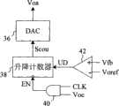
图6为图4中的ODC电路30的第二实施例,其包括数字模拟转换器(DAC)36、升降计数器38、与门40以及第一比较器42。第一比较器42比较回授信号Vfb及参考电压Voref产生比较信号UD给升降计数器38,与门40根据电源频率CLK及偏移校正信号Voc产生致能信号EN致能升降计数器38。频率CLK可为电源供应器内部产生的振荡信号。被触发后的升降计数器38根据比较信号UD决定计数值Scou,同时储存计数值Scou并传送给DAC 36,DAC 36将计数值Scou转换为偏移电压调整信号Voa给误差比较器14以调整其偏移,进而使回授信号Vfb接近参考电压Voref。参考电压Voref代表输出电压Vout的设计值,因此此ODC电路可将实际输出电压Vout的平均值拉近原先的设计值。FIG. 6 is a second embodiment of the ODC circuit 30 in FIG. 4 , which includes a digital-to-analog converter (DAC) 36 , an up-
图7显示图4中ODC电路30的第三实施例,其与图5的电路同样包括取样及维持电路34,但是用误差放大器44取代误差转导器32。误差放大器44放大回授信号Vfb及参考电压Voref之间的差值产生误差电压VEA,取样及维持电路34根据偏移校正信号Voc取样及储存误差电压VEA以产生偏移电压调整信号Voa。FIG. 7 shows a third embodiment of the ODC circuit 30 in FIG. 4 , which includes the sample and hold
以上对于本发明的较佳实施例所作的叙述为阐明的目的,而无意限定本发明精确地为所揭露的形式,基于以上的教导或从本发明的实施例学习而作修改或变化是可能的,实施例为解说本发明的原理以及让熟习该项技术者以各种实施例利用本发明在实际应用上而选择及叙述,本发明的保护范围应该以权利要求所界定的保护范围为准。The above description of the preferred embodiments of the present invention is for the purpose of illustration, and is not intended to limit the present invention to the disclosed form. It is possible to modify or change based on the above teachings or learning from the embodiments of the present invention. The embodiments are selected and described in order to explain the principles of the present invention and allow those skilled in the art to use the present invention in various embodiments for practical application. The protection scope of the present invention should be based on the protection scope defined in the claims.
Claims (23)
Priority Applications (1)
| Application Number | Priority Date | Filing Date | Title |
|---|---|---|---|
| CN201010249607.5ACN102377343B (en) | 2010-08-10 | 2010-08-10 | Fixed working time switching DC power supply and its control circuit and method |
Applications Claiming Priority (1)
| Application Number | Priority Date | Filing Date | Title |
|---|---|---|---|
| CN201010249607.5ACN102377343B (en) | 2010-08-10 | 2010-08-10 | Fixed working time switching DC power supply and its control circuit and method |
Publications (2)
| Publication Number | Publication Date |
|---|---|
| CN102377343Atrue CN102377343A (en) | 2012-03-14 |
| CN102377343B CN102377343B (en) | 2015-09-02 |
Family
ID=45795462
Family Applications (1)
| Application Number | Title | Priority Date | Filing Date |
|---|---|---|---|
| CN201010249607.5AActiveCN102377343B (en) | 2010-08-10 | 2010-08-10 | Fixed working time switching DC power supply and its control circuit and method |
Country Status (1)
| Country | Link |
|---|---|
| CN (1) | CN102377343B (en) |
Cited By (7)
| Publication number | Priority date | Publication date | Assignee | Title |
|---|---|---|---|---|
| CN103913648A (en)* | 2013-01-07 | 2014-07-09 | 致茂电子(苏州)有限公司 | Direct-current power supply unit and relevant photovoltaic inverter testing system |
| CN106253709A (en)* | 2015-06-05 | 2016-12-21 | 电力集成有限公司 | Relative to input line voltage change, there is the BJT driver that the storage time dynamically regulates |
| CN107508464A (en)* | 2017-08-28 | 2017-12-22 | 东莞市长工微电子有限公司 | A current feedback unilateral hysteresis control COT power management chip control circuit |
| CN108322065A (en)* | 2017-01-16 | 2018-07-24 | 三星电子株式会社 | Semiconductor devices and its operating method |
| CN110146845A (en)* | 2019-04-17 | 2019-08-20 | 杭州电子科技大学 | An event-driven fixed-time electromagnetic source location method |
| TWI678063B (en)* | 2018-12-03 | 2019-11-21 | 晶豪科技股份有限公司 | Constant on-time controller and buck converter using the same |
| CN113394974A (en)* | 2021-06-23 | 2021-09-14 | 江阴市新际科技有限公司 | COT switching converter with fixed frequency |
Citations (4)
| Publication number | Priority date | Publication date | Assignee | Title |
|---|---|---|---|---|
| CN1592059A (en)* | 2002-07-09 | 2005-03-09 | 罗姆股份有限公司 | DC/DC converter |
| US20080061750A1 (en)* | 2006-09-11 | 2008-03-13 | Micrel, Inc. | Ripple Generation In Buck Regulator Using Fixed On-Time Control To Enable The Use of Output Capacitor Having Any ESR |
| US7508181B2 (en)* | 2006-03-22 | 2009-03-24 | Anpec Electronics Corporation | Switching regulator capable of compensating output errors |
| JP2010035316A (en)* | 2008-07-28 | 2010-02-12 | Texas Instr Japan Ltd | Switching power unit |
- 2010
- 2010-08-10CNCN201010249607.5Apatent/CN102377343B/enactiveActive
Patent Citations (4)
| Publication number | Priority date | Publication date | Assignee | Title |
|---|---|---|---|---|
| CN1592059A (en)* | 2002-07-09 | 2005-03-09 | 罗姆股份有限公司 | DC/DC converter |
| US7508181B2 (en)* | 2006-03-22 | 2009-03-24 | Anpec Electronics Corporation | Switching regulator capable of compensating output errors |
| US20080061750A1 (en)* | 2006-09-11 | 2008-03-13 | Micrel, Inc. | Ripple Generation In Buck Regulator Using Fixed On-Time Control To Enable The Use of Output Capacitor Having Any ESR |
| JP2010035316A (en)* | 2008-07-28 | 2010-02-12 | Texas Instr Japan Ltd | Switching power unit |
Cited By (11)
| Publication number | Priority date | Publication date | Assignee | Title |
|---|---|---|---|---|
| CN103913648A (en)* | 2013-01-07 | 2014-07-09 | 致茂电子(苏州)有限公司 | Direct-current power supply unit and relevant photovoltaic inverter testing system |
| CN103913648B (en)* | 2013-01-07 | 2016-07-06 | 致茂电子(苏州)有限公司 | DC power supply and relevant photovoltaic inverter test system |
| CN106253709A (en)* | 2015-06-05 | 2016-12-21 | 电力集成有限公司 | Relative to input line voltage change, there is the BJT driver that the storage time dynamically regulates |
| US10574145B2 (en) | 2015-06-05 | 2020-02-25 | Power Integrations, Inc. | BJT driver with dynamic adjustment of storage time versus input line voltage variations |
| CN108322065A (en)* | 2017-01-16 | 2018-07-24 | 三星电子株式会社 | Semiconductor devices and its operating method |
| CN108322065B (en)* | 2017-01-16 | 2021-08-06 | 三星电子株式会社 | Semiconductor device and method of operating the same |
| CN107508464A (en)* | 2017-08-28 | 2017-12-22 | 东莞市长工微电子有限公司 | A current feedback unilateral hysteresis control COT power management chip control circuit |
| TWI678063B (en)* | 2018-12-03 | 2019-11-21 | 晶豪科技股份有限公司 | Constant on-time controller and buck converter using the same |
| CN110146845A (en)* | 2019-04-17 | 2019-08-20 | 杭州电子科技大学 | An event-driven fixed-time electromagnetic source location method |
| CN113394974A (en)* | 2021-06-23 | 2021-09-14 | 江阴市新际科技有限公司 | COT switching converter with fixed frequency |
| CN113394974B (en)* | 2021-06-23 | 2022-05-06 | 江阴市新际科技有限公司 | COT switching converter with fixed frequency |
Also Published As
| Publication number | Publication date |
|---|---|
| CN102377343B (en) | 2015-09-02 |
Similar Documents
| Publication | Publication Date | Title |
|---|---|---|
| JP5507980B2 (en) | Switching power supply control circuit, electronic device, and switching power supply control method | |
| TWI496387B (en) | Switching regulator and control circuit and control method thereof | |
| CN102377343B (en) | Fixed working time switching DC power supply and its control circuit and method | |
| TWI410773B (en) | Constant on time switching dc-dc power supply, and control circuit and method thereof | |
| US9529373B2 (en) | Switching regulator and control circuit and control method therefor | |
| KR101265387B1 (en) | Method of controlling a dc-dc converter in discontinuous mode | |
| US20170049150A1 (en) | Power converter, power control circuit and power control method of electronic cigarette | |
| US20150244262A1 (en) | Switching converter with constant on-time controller thereof | |
| US20170025952A1 (en) | Constant on-time pulse width control-based scheme including capabilities of fast transient response and adaptively adjusting on-time pulse width | |
| US8120340B2 (en) | Control device for an interleaving power factor corrector | |
| TWI426689B (en) | Switching regulator and control circuit and control method thereof | |
| TWI408883B (en) | Control circuit and bulk dc/dc converter in constant on-time mode | |
| CN102545662A (en) | Switch control circuit, converter using the same, and switch control method | |
| JP6767867B2 (en) | Resonant power converter and control method | |
| US9000735B2 (en) | DC-DC controller and operation method thereof | |
| TWI394356B (en) | Control device for dc-dc converter and related dc-dc converter | |
| CN114094824B (en) | Switching power supply circuit and control method | |
| US7193871B2 (en) | DC-DC converter circuit | |
| CN101238424B (en) | Switching regulator with variable slope compensation | |
| JP5228416B2 (en) | Constant current output control type switching regulator | |
| CN112865525A (en) | Adaptive frequency adjustment system | |
| JP2011097732A (en) | Step-up/down circuit | |
| CN115694186A (en) | Compensation Slope Adjustment in Voltage Converters | |
| CN102594108B (en) | Circuit and method for sampling reflected voltage of transformer of power converter | |
| JP5398422B2 (en) | Switching power supply |
Legal Events
| Date | Code | Title | Description |
|---|---|---|---|
| C06 | Publication | ||
| PB01 | Publication | ||
| C10 | Entry into substantive examination | ||
| SE01 | Entry into force of request for substantive examination | ||
| C14 | Grant of patent or utility model | ||
| GR01 | Patent grant |