CN102376665A - Semiconductor structure and manufacturing method thereof - Google Patents
Semiconductor structure and manufacturing method thereofDownload PDFInfo
- Publication number
- CN102376665A CN102376665ACN2010102659528ACN201010265952ACN102376665ACN 102376665 ACN102376665 ACN 102376665ACN 2010102659528 ACN2010102659528 ACN 2010102659528ACN 201010265952 ACN201010265952 ACN 201010265952ACN 102376665 ACN102376665 ACN 102376665A
- Authority
- CN
- China
- Prior art keywords
- layer
- bump
- metal
- semiconductor
- semiconductor structure
- Prior art date
- Legal status (The legal status is an assumption and is not a legal conclusion. Google has not performed a legal analysis and makes no representation as to the accuracy of the status listed.)
- Pending
Links
Images


Classifications
- H—ELECTRICITY
- H01—ELECTRIC ELEMENTS
- H01L—SEMICONDUCTOR DEVICES NOT COVERED BY CLASS H10
- H01L2224/00—Indexing scheme for arrangements for connecting or disconnecting semiconductor or solid-state bodies and methods related thereto as covered by H01L24/00
- H01L2224/73—Means for bonding being of different types provided for in two or more of groups H01L2224/10, H01L2224/18, H01L2224/26, H01L2224/34, H01L2224/42, H01L2224/50, H01L2224/63, H01L2224/71
- H01L2224/732—Location after the connecting process
- H01L2224/73201—Location after the connecting process on the same surface
- H01L2224/73203—Bump and layer connectors
- H01L2224/73204—Bump and layer connectors the bump connector being embedded into the layer connector
Landscapes
- Internal Circuitry In Semiconductor Integrated Circuit Devices (AREA)
Abstract
Description
Translated fromChinese技术领域technical field
本发明是关于一种半导体结构及其制造方法;具体而言,本发明是关于一种具有以半导体前段工艺形成的晶粒凸块(bump)的半导体结构及其制造方法。The present invention relates to a semiconductor structure and a manufacturing method thereof; specifically, the present invention relates to a semiconductor structure having grain bumps (bumps) formed by a semiconductor front-end process and a manufacturing method thereof.
背景技术Background technique
晶圆(wafer)是指制作半导体集成电路所使用的硅材质晶片,在经过沉积(deposition)、微影(photplithography)及蚀刻(etching)等处理以后,于其上形成许多个功能性晶粒(die),这些晶粒经过测试、切割、封装以后成为一颗颗集成电路晶片。Wafer (wafer) refers to the silicon wafer used in the production of semiconductor integrated circuits. After deposition (deposition), lithography (photplithography) and etching (etching) and other treatments, many functional crystal grains ( die), these grains are tested, cut, and packaged to become individual integrated circuit chips.
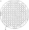
图1A为已知的半导体晶圆的示意图;图1B为已知的半导体装置的晶粒结构的示意图。如图1A所示,半导体晶圆1上形成有多个半导体装置的晶粒结构2。如图1B所示,每个晶粒结构2包含晶粒本体3、金属线路层4及凸块5。金属线路层4形成于晶粒本体2,凸块5形成于金属线路层4上而突出于晶粒本体3,进而可以与例如玻璃基板上的金属线路等其他元件电性连接。金属线路层4是在半导体前段工艺中形成,凸块5则是在半导体后段工艺中的晶圆凸块(wafer bumping)工艺中形成。为了节省成本起见,金属线路层4一般采用铝、铜等价格较低廉的金属材质,而为了防止凸块5因为氧化(生锈)而造成与其他元件之间的接触不良等现象,一般采用金等活性较低的金属材质来制作凸块5。FIG. 1A is a schematic diagram of a known semiconductor wafer; FIG. 1B is a schematic diagram of a grain structure of a known semiconductor device. As shown in FIG. 1A , a plurality of
然而,于半导体后段工艺中使用黄金材质来制作凸块5虽然能够有效地防止凸块5氧化,却具有成本昂贵、工艺复杂等缺点,在今日半导体工艺讲求工艺的高效率、低成本的趋势下,并不是一个理想的作法。However, although gold material is used to make
发明内容Contents of the invention
本发明的目的在于提供一种半导体结构及其制造方法,利用半导体前段工艺于晶粒上形成凸块,以达到简化工艺、节省成本等目的。The object of the present invention is to provide a semiconductor structure and a manufacturing method thereof, in which bumps are formed on crystal grains by utilizing semiconductor front-end technology, so as to achieve the purposes of simplifying the process and saving costs.
本发明的另一目的在于提供一种半导体结构及其制造方法,其将凸块工艺整合于半导体前段工艺并以半导体前段工艺常用的金属材料(例如铝、铜)作为凸块结构的主要材料,以达到工艺整合等目的。Another object of the present invention is to provide a semiconductor structure and a manufacturing method thereof, which integrates the bump process into the semiconductor front-end process and uses metal materials (such as aluminum and copper) commonly used in the semiconductor front-end process as the main material of the bump structure, In order to achieve the purpose of process integration.
本发明的半导体结构包含半导体晶圆,半导体晶圆上具有多个半导体装置的晶粒结构,其中每个晶粒结构包含晶粒本体、金属线路层、凸块及金属层。金属线路层形成于晶粒本体,凸块于半导体前段工艺形成于金属线路层上而突出于晶粒本体,金属层设置于凸块相对于金属线路层的一侧上,其中金属层的活性小于凸块的活性。本发明半导体结构的凸块是于半导体前段工艺制成,相对于利用半导体后段工艺所制成者,具有制造容易、节省成本等优点。The semiconductor structure of the present invention includes a semiconductor wafer on which there are multiple grain structures of semiconductor devices, wherein each grain structure includes a grain body, a metal circuit layer, a bump and a metal layer. The metal wiring layer is formed on the grain body, and the bump is formed on the metal wiring layer in the semiconductor front-end process to protrude from the grain body. The metal layer is arranged on the side of the bump opposite to the metal wiring layer, and the activity of the metal layer is less than Bump activity. The bumps of the semiconductor structure of the present invention are manufactured in the front-end process of the semiconductor, and have the advantages of easy manufacture and cost saving compared with those made by the back-end process of the semiconductor.
本发明的半导体结构制造方法包含下列步骤:提供半导体晶圆;于半导体晶圆上形成多个半导体装置晶粒结构,其中每个半导体装置晶粒结构包含晶粒本体;形成金属线路层于晶粒本体;利用半导体工艺形成凸块于金属线路层上,使凸块突出于晶粒本体;设置金属层于凸块相对于金属线路层的一侧上,其中金属层的活性小于凸块的活性。本发明于半导体前段工艺形成凸块,相对于在半导体后段工艺形成凸块的方式,具有简化工艺、节省成本等优点。The semiconductor structure manufacturing method of the present invention comprises the following steps: providing a semiconductor wafer; forming a plurality of semiconductor device grain structures on the semiconductor wafer, wherein each semiconductor device grain structure includes a grain body; forming a metal circuit layer on the grain The body; using semiconductor technology to form bumps on the metal circuit layer, so that the bumps protrude from the grain body; setting the metal layer on the side of the bumps opposite to the metal circuit layer, wherein the activity of the metal layer is smaller than that of the bumps. The invention forms bumps in the semiconductor front-end process, and has the advantages of simplifying the process and saving costs compared with the way of forming the bumps in the semiconductor back-end process.
附图说明Description of drawings
图1A为已知的半导体晶圆的示意图;FIG. 1A is a schematic diagram of a known semiconductor wafer;
图1B为已知的半导体装置的晶粒结构的示意图;1B is a schematic diagram of a known grain structure of a semiconductor device;
图2为本发明半导体装置的晶粒结构的一实施例的示意图;2 is a schematic diagram of an embodiment of the grain structure of the semiconductor device of the present invention;
图3为本发明半导体装置晶粒结构的另一实施例的示意图;3 is a schematic diagram of another embodiment of the grain structure of the semiconductor device of the present invention;
图4为图3所示半导体装置晶粒结构的使用示意图;FIG. 4 is a schematic diagram of the use of the grain structure of the semiconductor device shown in FIG. 3;
图5A为本发明半导体结构的制造方法的一实施例的示意图;5A is a schematic diagram of an embodiment of a method for manufacturing a semiconductor structure of the present invention;
图5B为图5A所示半导体结构的制造方法中形成凸块的一实施例的示意图;FIG. 5B is a schematic diagram of an embodiment of forming bumps in the manufacturing method of the semiconductor structure shown in FIG. 5A;
图6为本发明半导体结构的制造方法的另一实施例的示意图;6 is a schematic diagram of another embodiment of the manufacturing method of the semiconductor structure of the present invention;
图7A为本发明半导体结构的制造方法的又一实施例的示意图;以及7A is a schematic diagram of another embodiment of the method for manufacturing a semiconductor structure of the present invention; and
图7B为图7A所示半导体结构的制造方法中形成绝缘层的步骤的一实施例的示意图。FIG. 7B is a schematic diagram of an embodiment of the step of forming an insulating layer in the manufacturing method of the semiconductor structure shown in FIG. 7A .
主要元件符号说明Description of main component symbols
10晶粒本体10 grain body
11表面11 surfaces
20金属线路层20 metal circuit layers
30凸块30 bumps
31端面31 end faces
32侧壁32 side walls
40金属层40 metal layers
50绝缘层50 insulation layers
51覆盖部51 Covering Department
60基板60 substrates
61导电膜层61 conductive film layer
70导电层70 conductive layer
71绝缘胶材71 insulating glue
72导电粒子72 conductive particles
73导通路径73 conduction path
100金属材料100 metal materials
200绝缘材料200 insulating material
具体实施方式Detailed ways
本发明提供一种半导体结构及其制造方法。在较佳实施例中,本发明的半导体结构及其制造方法可使用于任何需要凸块结构的半导体相关装置及工艺中,例如半导体装置的集成电路或液晶显示器的驱动电路等。The invention provides a semiconductor structure and a manufacturing method thereof. In a preferred embodiment, the semiconductor structure and its manufacturing method of the present invention can be used in any semiconductor-related devices and processes that require a bump structure, such as integrated circuits of semiconductor devices or driving circuits of liquid crystal displays.
本发明的半导体结构包含半导体晶圆,半导体晶圆上具有多个半导体装置的晶粒结构。晶粒结构较佳通过重复沉积、微影及蚀刻等半导体工艺而形成。图2为本发明半导体装置的晶粒结构的一实施例的示意图。如图2所示,半导体装置晶粒结构包含晶粒本体10、金属线路层20、凸块30及金属层40。金属线路层20形成于晶粒本体10中,可以为晶粒本体10中的多个金属线路层中的一个,一般为晶粒本体10中最上层用以作为与其他装置接触的金属层。金属线路层20较佳采用沉积、微影及蚀刻等半导体工艺而形成。在本实施例中,金属线路层20的材质为铝;然而在其他本实施例中,可以采用例如铜等其他金属或合金材质。The semiconductor structure of the present invention includes a semiconductor wafer, and the semiconductor wafer has a plurality of grain structures of semiconductor devices. The grain structure is preferably formed by repeated semiconductor processes such as deposition, lithography and etching. FIG. 2 is a schematic diagram of an embodiment of the grain structure of the semiconductor device of the present invention. As shown in FIG. 2 , the semiconductor device grain structure includes a
凸块30形成于金属线路层20上而突出于晶粒本体10的表面11,其中凸块30与金属线路层20皆于半导体前段工艺形成。亦即,凸块30是于半导体晶圆制造厂利用既有的晶粒制造设备所形成。凸块30较佳采用沉积、微影及蚀刻等半导体工艺而形成。在本实施例中,凸块30采用与金属线路层20相同的铝材质;然而在其他实施例中,凸块30的材质可以与金属线路层20不同,并可采用例如铜等其他金属材质。于一实施例中,凸块30及金属线路层20是整合为单一结构,其是利用沉积、微影、蚀刻由单一金属材料层所形成。于另一实施例中,凸块30及金属线路层20为个别结构,其是利用沉积、微影、蚀刻由不同层的金属材料层所形成。The
金属层40设置于凸块30远离金属线路层20的一端的端面31上,其中金属层40的活性小于凸块30的活性。金属层40较佳采用半导体工艺或电镀等工艺而形成。在本实施例中,金属层40的材质为金;然而在其他本实施例中,可以采用其他惰性金属材质。The
相较于现有技术,本发明半导体结构的凸块30是于半导体前段工艺中形成,尤其是整合前段工艺中常用的金属材料,例如使用比金还更符合经济效益的铝或铜等作为凸块30的主要材料,达到工艺相容又节省材料成本的优点。再者,本发明又利用具有较高导电性及较低活性的金作为金属层40形成于铝或铜材料的凸块30的表面上,不仅强化凸块30与其他装置的接触效果,更可避免凸块30氧化受损。Compared with the prior art, the
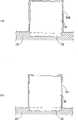
图3为本发明半导体装置晶粒结构的另一实施例的示意图。如图3所示,此晶粒结构除了前述的晶粒本体10、金属线路层20、凸块30及金属层40以外,还包含绝缘层50。绝缘层50围绕凸块30的侧边而设置于凸块30的侧壁32上,以对凸块30提供绝缘、抗氧化(防锈)等作用。在较佳实施例中,绝缘层50往凸块30的端面31的中央部分延伸而覆盖端面31周缘的一部分,使绝缘层50一端的覆盖部51夹设于凸块30与金属层40之间,以确保凸块30与金属层40相互衔接的部分不会向外曝露,进而达到抗氧化的效果。然而在其他实施例中,可以不设置覆盖部51,而仅于侧壁32上设置绝缘层50。绝缘层50较佳采用沉积、微影及蚀刻等半导体前段工艺而形成。绝缘层50可以采用例如氮化硅、二氧化硅、氮氧化硅等绝缘材质,且具有一定的厚度,以达到凸块30的绝缘、抗氧化等效果。FIG. 3 is a schematic diagram of another embodiment of the grain structure of the semiconductor device of the present invention. As shown in FIG. 3 , the grain structure includes an insulating
图4为图3所示半导体装置晶粒结构的使用示意图。如图4所示,基板60包含相隔设置的导电膜层61,每个凸块30对应于一个导电膜层61。导电层70连接于基板60与晶粒本体10之间,其中包含绝缘胶材71及导电粒子72,使每个凸块30上的金属层40通过导电粒子72与对应的导电膜层61相互电性连接。如图4所示,即使两个凸块30之间的导电粒子72排列形成导通路径73,也可以通过形成于凸块30周缘的绝缘层50所提供的绝缘来使得两个相邻的凸块30之间不会形成短路,因而可避免两个相邻的凸块30之间容易出现短路的问题。在较佳实施例中,基板60可为玻璃材质,导电膜层61可为形成于基板60上的金属电极层,导电层70则可采用异方性导电胶膜;然而在其他实施例中,可以分别采用其他材质。FIG. 4 is a schematic view showing the use of the grain structure of the semiconductor device shown in FIG. 3 . As shown in FIG. 4 , the
图5A为本发明半导体结构的制造方法的一实施例的示意图。如图5A所示,步骤A1形成半导体装置的晶粒结构于半导体晶圆上,其中每个半导体装置的晶粒结构包含晶粒本体10。具体而言,晶粒结构较佳通过重复沉积、微影及蚀刻等半导体工艺而形成具有晶粒形式的预定功能性半导体装置。此半导体装置可为任何后续欲形成凸块结构以与其他装置电连接的集成电路装置,例如半导体集成电路或液晶显示器的驱动电路等。步骤A2形成金属线路层20于晶粒本体10。具体而言,金属线路层20形成于晶粒本体10中,可以为晶粒本体中的多个金属线路层中的一个,一般为晶粒结构的最上/外层的金属线路层。金属线路层20较佳采用沉积、微影及蚀刻等半导体前段工艺而形成。举例而言,形成金属线路层20的步骤包含利用微影技术于半导体晶圆的各晶粒结构上界定金属线路层的位置,然后毯覆式(全面地)沉积金属材料层,以及蚀刻/研磨金属材料层,而形成嵌于晶粒本体10的金属线路层20,如图5A的A2所示。在本实施例中,金属线路层20的材质为铝;然而在其他本实施例中,可以采用例如铜等其他金属材质。FIG. 5A is a schematic diagram of an embodiment of a method for manufacturing a semiconductor structure of the present invention. As shown in FIG. 5A , step A1 forms the grain structure of semiconductor devices on the semiconductor wafer, wherein each grain structure of the semiconductor device includes a
步骤A3利用半导体前段工艺形成凸块30于金属线路层20上,使凸块30突出于晶粒本体。In step A3 , the
图5B为图5A所示半导体结构的制造方法中形成凸块30的步骤A3的一实施例的示意图。在本实施例中,如图5B所示,图5A的步骤A3中形成凸块30的步骤包含:步骤A31毯覆式沉积活性大于金的金属材料层100于金属线路层20上。具体而言,金属材料层100覆盖于晶圆上各晶粒本体10的表面与金属线路层20上。步骤A32利用光学微影及蚀刻技术处理金属材料层100,以形成凸块20于金属线路层上。具体而言,凸块30形成于金属线路层20上而突出于晶粒本体10的表面。在本实施例中,凸块30采用与金属线路层20相同的铝材质;然而在其他实施例中,凸块30的材质可以与金属线路层20不同,并可采用例如铜等其他金属材质。于此实施例中,是利用于半导体前段工艺分别形成金属线路层20及凸块30,尤其是整合前段工艺中常用的金属材料,例如使用比金还更符合经济效益的铝或铜等作为凸块30的主要材料,达到工艺相容又节省材料成本的优点。亦即,凸块30是于半导体晶圆制造厂利用既有的晶粒制造设备所形成,减少封装厂后段工艺中相关凸块制造的设备及材料成本。FIG. 5B is a schematic diagram of an embodiment of the step A3 of forming the
步骤A4设置金属层40于凸块30相对于金属线路层20的一侧上,其中金属层40的活性小于凸块30的活性。具体而言,金属层40设置于凸块30远离金属线路层40的一端的端面上。金属层40较佳采用半导体工艺或电镀等工艺而形成。在本实施例中,金属层40的材质为金;然而在其他本实施例中,可以采用其他惰性金属材质。亦即,本发明又利用具有较高导电性及较低活性的金作为金属层40形成于铝或铜材料的凸块30的表面上,不仅强化凸块30与其他装置的接触效果,更可避免凸块30氧化受损。Step A4 disposes the
相较于现有技术,本发明于半导体前段工艺即利用较易取得硬成本较低廉的金属材料完成凸块的形成,避免了于半导体后段工艺中利用昂贵的金作为凸块的主要材料,具有工艺整合、节省成本等优点。再者,本发明仅应用少量如金的金属层40于凸块30的表面,以更符合经济效益方式增强晶粒结构与其他装置的电接触。Compared with the prior art, the present invention uses metal materials that are easier to obtain and lower in cost in the semiconductor front-end process to complete the formation of the bumps, avoiding the use of expensive gold as the main material of the bumps in the semiconductor back-end process, It has the advantages of process integration and cost saving. Furthermore, the present invention only applies a small amount of
在其他实施例中,可用其他方式形成金属线路层及凸块。图6为本发明半导体结构的制造方法的另一实施例的示意图。如图6所示,步骤B1形成半导体装置的晶粒结构于半导体晶圆上,其中每个半导体装置的晶粒结构包含晶粒本体10。于此,步骤B1与前述步骤A1类似,不再赘述。步骤B2沉积厚度与凸块30的高度相当的金属材料层100于晶粒本体10上。步骤B3利用光学微影及蚀刻技术处理金属材料层100,以利用金属材料层分别形成金属线路层20及凸块30。亦即,由步骤B2及B3可知,金属线路层20及凸块30是利用同一金属材料层100所形成,而利用半导体前段工艺的微影、蚀刻等技术分别界定出金属线路层20及凸块30。步骤B4设置金属层40于凸块30相对于金属线路层20的一侧上,其中金属层的活性小于凸块的活性。步骤B4与前述步骤A4类似,于此不再赘述。In other embodiments, the metal wiring layer and the bumps can be formed in other ways. FIG. 6 is a schematic diagram of another embodiment of the manufacturing method of the semiconductor structure of the present invention. As shown in FIG. 6 , step B1 forms the grain structure of semiconductor devices on the semiconductor wafer, wherein each grain structure of the semiconductor device includes a
图7A为本发明半导体结构的制造方法的又一实施例的示意图。如图7A所示,步骤C1形成半导体装置的晶粒结构于半导体晶圆上,其中每个半导体装置的晶粒结构包含晶粒本体10。于此,步骤C1与前述步骤A1类似,不再赘述。步骤C2形成金属线路层20于晶粒本体10。步骤C3利用半导体前段工艺形成凸块30于金属线路层20上,使凸块30突出于晶粒本体。需注意,形成金属线路层20与凸块30的方式可参考前述步骤A2及A3或步骤B2及B3的相关说明,于此不再赘述。于本实施例中,本方法更包含步骤C4形成绝缘层50于凸块30的侧壁。在较佳实施例中,如图7B所示,步骤C4中形成绝缘层的步骤包含:步骤C41共形地沉积绝缘材料200于包含凸块30在内的半导体晶圆上,使绝缘材料200均匀地沿着晶粒本体及凸块的表面而设置,以承袭晶粒本体具有凸块突出的形状。步骤C42蚀刻绝缘材料200以形成绝缘层50于凸块30的侧壁上,而移除晶粒本体表面及凸块的其他部分上的绝缘材料200。举例而言,可利用半导体前段工艺形成间隙壁的方式,无需微影工艺即可利用等向性蚀刻形成绝缘层50于凸块30的裸露侧壁上。选替地,可利用微影技术界定凸块30欲与后续形成的金属层40(见步骤C5)的裸露部分,再利用蚀刻技术移除凸块30表面上的部分绝缘材料200,而形成如图7A的步骤C4的绝缘层50。步骤C5设置金属层于凸块相对于金属线路层的一侧上,其中金属层的活性小于凸块的活性。步骤C5与前述步骤A4、B4类似,于此不再赘述。FIG. 7A is a schematic diagram of yet another embodiment of the manufacturing method of the semiconductor structure of the present invention. As shown in FIG. 7A , step C1 forms the grain structures of semiconductor devices on the semiconductor wafer, wherein each grain structure of semiconductor devices includes a
具体而言,绝缘层围绕凸块的侧边而设置于凸块的侧壁上,以对凸块提供绝缘、抗氧化等作用。在较佳实施例中,绝缘层往端面的中央部分延伸而覆盖端面周缘的一部分,使绝缘层一端的覆盖部夹设于凸块与金属层之间,以确保凸块与金属层相互衔接的部分不会向外曝露,进而达到抗氧化的效果。然而在其他实施例中,可以不设置覆盖部,而仅于侧壁上设置绝缘层。绝缘层可以采用例如氮化硅、二氧化硅等绝缘材质,且具有一定的厚度,以达到凸块的绝缘、抗氧化等效果。此外,由于凸块的侧壁上设有绝缘层,因此能够防止相邻的凸块之间出现短路(如图4所示)。Specifically, the insulating layer is disposed on the sidewall of the bump around the side of the bump, so as to provide insulation, anti-oxidation and other functions for the bump. In a preferred embodiment, the insulating layer extends toward the central part of the end surface to cover a part of the periphery of the end surface, so that the covering portion at one end of the insulating layer is sandwiched between the bump and the metal layer, so as to ensure that the bump and the metal layer are connected to each other. Part of it will not be exposed to the outside, so as to achieve the effect of anti-oxidation. However, in other embodiments, the covering portion may not be provided, but only the insulating layer is provided on the sidewall. The insulating layer can be made of insulating materials such as silicon nitride and silicon dioxide, and has a certain thickness, so as to achieve the effects of insulation and oxidation resistance of the bumps. In addition, since the insulating layer is provided on the sidewall of the bump, short circuit between adjacent bumps can be prevented (as shown in FIG. 4 ).
本发明已由上述相关实施例加以描述,然而上述实施例仅为实施本发明的范例。必需指出的是,已揭露的实施例并未限制本发明的范围。相反地,包含于权利要求书的精神及范围的修改及均等设置均包含于本发明的范围内。The present invention has been described by the above-mentioned related embodiments, however, the above-mentioned embodiments are only examples for implementing the present invention. It must be pointed out that the disclosed embodiments do not limit the scope of the present invention. On the contrary, modifications and equivalent arrangements included in the spirit and scope of the claims are included in the scope of the present invention.
Claims (10)
Translated fromChinesePriority Applications (1)
| Application Number | Priority Date | Filing Date | Title |
|---|---|---|---|
| CN2010102659528ACN102376665A (en) | 2010-08-25 | 2010-08-25 | Semiconductor structure and manufacturing method thereof |
Applications Claiming Priority (1)
| Application Number | Priority Date | Filing Date | Title |
|---|---|---|---|
| CN2010102659528ACN102376665A (en) | 2010-08-25 | 2010-08-25 | Semiconductor structure and manufacturing method thereof |
Publications (1)
| Publication Number | Publication Date |
|---|---|
| CN102376665Atrue CN102376665A (en) | 2012-03-14 |
Family
ID=45795044
Family Applications (1)
| Application Number | Title | Priority Date | Filing Date |
|---|---|---|---|
| CN2010102659528APendingCN102376665A (en) | 2010-08-25 | 2010-08-25 | Semiconductor structure and manufacturing method thereof |
Country Status (1)
| Country | Link |
|---|---|
| CN (1) | CN102376665A (en) |
Citations (4)
| Publication number | Priority date | Publication date | Assignee | Title |
|---|---|---|---|---|
| CN1437256A (en)* | 2002-02-07 | 2003-08-20 | 日本电气株式会社 | Semiconductor element and its manufacturing method, and semiconductor device and its manufacturing method |
| US6624504B1 (en)* | 1999-10-29 | 2003-09-23 | Hitachi, Ltd. | Semiconductor device and method for manufacturing the same |
| US7732253B1 (en)* | 2006-08-14 | 2010-06-08 | Rf Micro Devices, Inc. | Flip-chip assembly with improved interconnect |
| US20100181650A1 (en)* | 2009-01-20 | 2010-07-22 | Renesas Technology Corp. | Semiconductor integrated circuit device and a method for manufacturing a semiconductor integrated circuit device |
- 2010
- 2010-08-25CNCN2010102659528Apatent/CN102376665A/enactivePending
Patent Citations (4)
| Publication number | Priority date | Publication date | Assignee | Title |
|---|---|---|---|---|
| US6624504B1 (en)* | 1999-10-29 | 2003-09-23 | Hitachi, Ltd. | Semiconductor device and method for manufacturing the same |
| CN1437256A (en)* | 2002-02-07 | 2003-08-20 | 日本电气株式会社 | Semiconductor element and its manufacturing method, and semiconductor device and its manufacturing method |
| US7732253B1 (en)* | 2006-08-14 | 2010-06-08 | Rf Micro Devices, Inc. | Flip-chip assembly with improved interconnect |
| US20100181650A1 (en)* | 2009-01-20 | 2010-07-22 | Renesas Technology Corp. | Semiconductor integrated circuit device and a method for manufacturing a semiconductor integrated circuit device |
Similar Documents
| Publication | Publication Date | Title |
|---|---|---|
| US10840204B2 (en) | Semiconductor device for bonding conductive layers exposed from surfaces of respective interconnection layers | |
| TWI594339B (en) | Semiconductor device and manufacturing method thereof | |
| US9691739B2 (en) | Semiconductor device and method of manufacturing same | |
| US8154134B2 (en) | Packaged electronic devices with face-up die having TSV connection to leads and die pad | |
| US8497558B2 (en) | System and method for wafer level packaging | |
| TWI364820B (en) | Chip structure | |
| JP5129939B2 (en) | Manufacturing method of semiconductor device | |
| KR20200034078A (en) | Semiconductor device and semiconductor package including the same | |
| CN101335280A (en) | Image sensor package and manufacturing method thereof | |
| TWI234261B (en) | Method of forming wafer backside interconnects | |
| JP2008294405A (en) | Semiconductor device and manufacturing method thereof | |
| US20080079134A1 (en) | Chip package, chip structure and manufacturing process thereof | |
| US12362311B2 (en) | Anisotropic conductive film with carbon-based conductive regions having void space and related semiconductor device assemblies and methods | |
| CN101404268A (en) | Semiconductor element and bump manufacturing method | |
| CN105810596A (en) | Fabrication method of etched surface acoustic filter chip package structure | |
| JP2024001301A (en) | Structure and method for semiconductor packaging | |
| US11011491B2 (en) | Semiconductor device packages and methods of manufacturing the same | |
| CN102376665A (en) | Semiconductor structure and manufacturing method thereof | |
| JP2011249562A (en) | Semiconductor apparatus and manufacturing method thereof | |
| CN109411407A (en) | A kind of semiconductor devices and preparation method thereof | |
| CN101330088A (en) | Integrated circuit package and manufacturing method thereof | |
| US20120018880A1 (en) | Semiconductor structure and manufacturing method thereof | |
| CN105826214B (en) | A kind of preparation method of bonded wafer structure | |
| CN100447973C (en) | Chip Structure and Manufacturing Process | |
| CN119028837A (en) | Semiconductor device, preparation method and packaging method, semiconductor packaging structure |
Legal Events
| Date | Code | Title | Description |
|---|---|---|---|
| C06 | Publication | ||
| PB01 | Publication | ||
| C10 | Entry into substantive examination | ||
| SE01 | Entry into force of request for substantive examination | ||
| C02 | Deemed withdrawal of patent application after publication (patent law 2001) | ||
| WD01 | Invention patent application deemed withdrawn after publication | Application publication date:20120314 |