CN102375185A - Optical transceiver and manufacturing method thereof - Google Patents
Optical transceiver and manufacturing method thereofDownload PDFInfo
- Publication number
- CN102375185A CN102375185ACN2010102589385ACN201010258938ACN102375185ACN 102375185 ACN102375185 ACN 102375185ACN 2010102589385 ACN2010102589385 ACN 2010102589385ACN 201010258938 ACN201010258938 ACN 201010258938ACN 102375185 ACN102375185 ACN 102375185A
- Authority
- CN
- China
- Prior art keywords
- substrate
- fixing
- hole
- light
- bracket
- Prior art date
- Legal status (The legal status is an assumption and is not a legal conclusion. Google has not performed a legal analysis and makes no representation as to the accuracy of the status listed.)
- Granted
Links
Images


Classifications
- H—ELECTRICITY
- H01—ELECTRIC ELEMENTS
- H01S—DEVICES USING THE PROCESS OF LIGHT AMPLIFICATION BY STIMULATED EMISSION OF RADIATION [LASER] TO AMPLIFY OR GENERATE LIGHT; DEVICES USING STIMULATED EMISSION OF ELECTROMAGNETIC RADIATION IN WAVE RANGES OTHER THAN OPTICAL
- H01S5/00—Semiconductor lasers
- H01S5/40—Arrangement of two or more semiconductor lasers, not provided for in groups H01S5/02 - H01S5/30
- H01S5/4025—Array arrangements, e.g. constituted by discrete laser diodes or laser bar
- G—PHYSICS
- G02—OPTICS
- G02B—OPTICAL ELEMENTS, SYSTEMS OR APPARATUS
- G02B6/00—Light guides; Structural details of arrangements comprising light guides and other optical elements, e.g. couplings
- G02B6/24—Coupling light guides
- G02B6/42—Coupling light guides with opto-electronic elements
- G02B6/4201—Packages, e.g. shape, construction, internal or external details
- G02B6/4246—Bidirectionally operating package structures
- H—ELECTRICITY
- H01—ELECTRIC ELEMENTS
- H01L—SEMICONDUCTOR DEVICES NOT COVERED BY CLASS H10
- H01L2224/00—Indexing scheme for arrangements for connecting or disconnecting semiconductor or solid-state bodies and methods related thereto as covered by H01L24/00
- H01L2224/01—Means for bonding being attached to, or being formed on, the surface to be connected, e.g. chip-to-package, die-attach, "first-level" interconnects; Manufacturing methods related thereto
- H01L2224/42—Wire connectors; Manufacturing methods related thereto
- H01L2224/47—Structure, shape, material or disposition of the wire connectors after the connecting process
- H01L2224/48—Structure, shape, material or disposition of the wire connectors after the connecting process of an individual wire connector
- H01L2224/4805—Shape
- H01L2224/4809—Loop shape
- H01L2224/48091—Arched
- H—ELECTRICITY
- H01—ELECTRIC ELEMENTS
- H01S—DEVICES USING THE PROCESS OF LIGHT AMPLIFICATION BY STIMULATED EMISSION OF RADIATION [LASER] TO AMPLIFY OR GENERATE LIGHT; DEVICES USING STIMULATED EMISSION OF ELECTROMAGNETIC RADIATION IN WAVE RANGES OTHER THAN OPTICAL
- H01S5/00—Semiconductor lasers
- H01S5/02—Structural details or components not essential to laser action
- H01S5/022—Mountings; Housings
- H01S5/023—Mount members, e.g. sub-mount members
- H01S5/02325—Mechanically integrated components on mount members or optical micro-benches
- H01S5/02326—Arrangements for relative positioning of laser diodes and optical components, e.g. grooves in the mount to fix optical fibres or lenses
- H—ELECTRICITY
- H01—ELECTRIC ELEMENTS
- H01S—DEVICES USING THE PROCESS OF LIGHT AMPLIFICATION BY STIMULATED EMISSION OF RADIATION [LASER] TO AMPLIFY OR GENERATE LIGHT; DEVICES USING STIMULATED EMISSION OF ELECTROMAGNETIC RADIATION IN WAVE RANGES OTHER THAN OPTICAL
- H01S5/00—Semiconductor lasers
- H01S5/02—Structural details or components not essential to laser action
- H01S5/022—Mountings; Housings
- H01S5/0235—Method for mounting laser chips
- H01S5/02355—Fixing laser chips on mounts
- H01S5/0237—Fixing laser chips on mounts by soldering
- Y—GENERAL TAGGING OF NEW TECHNOLOGICAL DEVELOPMENTS; GENERAL TAGGING OF CROSS-SECTIONAL TECHNOLOGIES SPANNING OVER SEVERAL SECTIONS OF THE IPC; TECHNICAL SUBJECTS COVERED BY FORMER USPC CROSS-REFERENCE ART COLLECTIONS [XRACs] AND DIGESTS
- Y10—TECHNICAL SUBJECTS COVERED BY FORMER USPC
- Y10T—TECHNICAL SUBJECTS COVERED BY FORMER US CLASSIFICATION
- Y10T29/00—Metal working
- Y10T29/49—Method of mechanical manufacture
- Y10T29/49002—Electrical device making
- Y10T29/49117—Conductor or circuit manufacturing
Landscapes
- Physics & Mathematics (AREA)
- Condensed Matter Physics & Semiconductors (AREA)
- General Physics & Mathematics (AREA)
- Electromagnetism (AREA)
- Optics & Photonics (AREA)
- Optical Couplings Of Light Guides (AREA)
- Semiconductor Lasers (AREA)
- Light Receiving Elements (AREA)
Abstract
Translated fromChinese
Description
Translated fromChinese技术领域technical field
本发明涉及一种光收发器及其制造方法,尤其涉及一种光学元件与透镜精确对位的光收发器制造方法。The invention relates to an optical transceiver and a manufacturing method thereof, in particular to a manufacturing method of an optical transceiver in which an optical element and a lens are precisely aligned.
背景技术Background technique
光通信逐渐成为一项新兴且具有发展潜力的技术,正被人们普遍使用,其主要借由光纤传输数据,可以达到更快速且足够大的通信频宽,同时也能保持传输的品质。通常,光通信主要利用光收发器将光纤线路中的光信号与电子设备中的电信号进行相互转换,从而完成数据的快速传输。可见,光收发器性能的好坏直接决定数据传输的质量。然而,光收发器中镭射芯片与透镜的对位精确度是判定其性能好坏的一个重要因素。Optical communication has gradually become an emerging technology with potential for development, and is being widely used by people. It mainly uses optical fiber to transmit data, which can achieve faster and large enough communication bandwidth while maintaining the quality of transmission. Usually, optical communication mainly uses optical transceivers to convert optical signals in optical fiber lines and electrical signals in electronic equipment, so as to complete fast data transmission. It can be seen that the performance of the optical transceiver directly determines the quality of data transmission. However, the alignment accuracy of the laser chip and the lens in the optical transceiver is an important factor to determine its performance.
因此,如何实现光收发器中镭射芯片与透镜的精确对位成为光收发器设计的一大课题。Therefore, how to realize the precise alignment of the laser chip and the lens in the optical transceiver has become a major issue in the design of the optical transceiver.
发明内容Contents of the invention
有鉴于此,需提供一种光收发器,其中,镭射芯片与透镜具有较高的对位精准度。In view of this, it is necessary to provide an optical transceiver, wherein the laser chip and the lens have high alignment accuracy.
此外,还需提供一种光收发器制造方法,利用简单的制程实现镭射芯片之发光元件与透镜的精确对位。In addition, it is also necessary to provide a manufacturing method for the optical transceiver, which can achieve precise alignment between the light-emitting element and the lens of the laser chip by using a simple manufacturing process.
本发明实施方式中一种光收发器,用于进行光电信号转换,包括基板、多个镭射芯片、支架以及多个透镜。所述基板包括多个透光孔、多个收容槽及多个固定孔,每一个收容槽的半径大于每一个透光孔的半径,每一个透光孔与每一个收容槽连通并同轴。镭射芯片分别设置于所述收容槽内,用于收发所述光电信号。支架包括一对侧壁,每一个侧壁包括外表面、固定面、通孔及固定柱,所述固定面与所述基板相对并粘贴于所述基板,所述通孔贯穿于所述固定面与所述外表面之间,所述固定柱与所述固定孔配合以加强所述支架与所述基板之间连接的稳定性。透镜安装于所述支架并位于所述侧壁之间,且与所述透光孔对应设置,用于接收所述镭射芯片发出的信号。An optical transceiver in an embodiment of the present invention is used for photoelectric signal conversion, and includes a substrate, a plurality of laser chips, a bracket and a plurality of lenses. The base plate includes a plurality of light-transmitting holes, a plurality of receiving grooves and a plurality of fixing holes, the radius of each receiving groove is larger than that of each light-transmitting hole, and each light-transmitting hole communicates with and is coaxial with each receiving groove. The laser chips are respectively arranged in the receiving grooves for sending and receiving the photoelectric signals. The bracket includes a pair of side walls, each side wall includes an outer surface, a fixing surface, a through hole and a fixing column, the fixing surface is opposite to the substrate and pasted on the substrate, and the through hole penetrates through the fixing surface Between the outer surface, the fixing posts cooperate with the fixing holes to enhance the stability of the connection between the bracket and the base plate. The lens is installed on the bracket and is located between the side walls, and is arranged corresponding to the light-transmitting hole for receiving the signal sent by the laser chip.
本发明实施方式中的一种光收发器制造方法,包括提供基板,所述基板包括多个透光孔、多个收容槽及多个固定孔,其中,每一个收容槽的半径大于每一个透光孔的半径,每一个透光孔与每一个收容槽连通并同轴。将镭射芯片焊接于所述收容槽内。将驱动芯片焊接于所述基板,用于驱动所述镭射芯片。提供支架,所述支架包括一对侧壁,每一个侧壁包括外表面、固定面、通孔及固定柱,所述固定面与所述基板相对并粘贴于所述基板,所述通孔贯穿于所述固定面与所述外表面之间,所述固定柱与所述固定孔配合以加强所述支架与所述基板之间连接的稳定性。安装多个透镜于所述支架上,所述透镜位于所述侧壁之间,且与所述透光孔对应设置,用于接收所述镭射芯片发出的信号。将所述固定面进行点胶。将固定柱安装于所述固定孔内,并通过热固化制程将所述支架粘贴定位于所述基板。A method of manufacturing an optical transceiver in an embodiment of the present invention includes providing a substrate, the substrate including a plurality of light-transmitting holes, a plurality of receiving grooves, and a plurality of fixing holes, wherein the radius of each receiving groove is larger than that of each transparent hole. The radius of the light hole, each light transmission hole communicates with each receiving groove and is coaxial. The laser chip is welded in the accommodating groove. The driving chip is soldered to the substrate for driving the laser chip. Provide a bracket, the bracket includes a pair of side walls, each side wall includes an outer surface, a fixing surface, a through hole and a fixing post, the fixing surface is opposite to the substrate and stuck to the substrate, and the through hole penetrates Between the fixing surface and the outer surface, the fixing column cooperates with the fixing hole to enhance the stability of the connection between the bracket and the base plate. A plurality of lenses are installed on the bracket, and the lenses are located between the side walls and corresponding to the light transmission holes, and are used for receiving signals from the laser chip. Glue is dispensed on the fixed surface. The fixing post is installed in the fixing hole, and the bracket is pasted and positioned on the base plate through a thermal curing process.
本发明的光收发器通过所述通孔的设置使得支架在很短的时间内被固定于基板,从而防止在热固定制程过程中,支架相对基板的位置漂移,进而实现透镜与镭射芯片之间精确对位,实现高精度的封装技术。同时,固定柱与固定孔的配合加强了支架与基板之间的连接的稳定性,当基板发生变形时,固定柱与固定孔的配合能够有效防止支架与基板分离,提高产品良率。The optical transceiver of the present invention enables the support to be fixed to the substrate in a very short time through the setting of the through hole, thereby preventing the position of the support from drifting relative to the substrate during the heat fixing process, thereby realizing the gap between the lens and the laser chip. Precise alignment to achieve high-precision packaging technology. At the same time, the cooperation of the fixing post and the fixing hole strengthens the stability of the connection between the bracket and the substrate. When the substrate is deformed, the cooperation of the fixing post and the fixing hole can effectively prevent the separation of the bracket and the substrate and improve the product yield.
附图说明Description of drawings
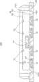
图1所示为本发明光收发器的结构示意图。FIG. 1 is a schematic structural diagram of an optical transceiver of the present invention.
图2所示为本发明光收发器之基板的结构示意图。FIG. 2 is a schematic structural diagram of the substrate of the optical transceiver of the present invention.
图3所示为本发明光收发器之设置镭射芯片与驱动芯片的基板的示意图。FIG. 3 is a schematic diagram of a substrate on which a laser chip and a driver chip are arranged in the optical transceiver of the present invention.
图4所示为本发明光收发器之设置镭射芯片与驱动芯片的基板与支架的分解示意图。FIG. 4 is an exploded schematic view of the substrate and support for the laser chip and driver chip of the optical transceiver of the present invention.
主要元件符号说明Description of main component symbols
光收发器 200
基板 20
第一表面 22
第二表面 23
透光孔 24
收容槽 26
固定孔 28Fixing
焊垫 29Welding
镭射芯片 30
发光元件 301
支架 40Bracket 40
主体 41
侧壁 42
通孔 420
固定柱 422Fixed
外表面 423
固定面 424Fixed
透镜 50
驱动芯片 60
具体实施方式Detailed ways
图1所示为本发明光收发器200结构的示意图。本实施方式中,光收发器200用于进行光电信号转换,其包括基板20、多个镭射芯片30、驱动芯片60、支架40以及多个透镜50。FIG. 1 is a schematic diagram of the structure of an
图2所示为本发明光收发器之基板20的结构示意图。基板20包括第一表面22、与第一表面22相对的第二表面23、多个透光孔24、多个收容槽26及多个固定孔28。所述固定孔28包围所收容槽26,且对称分布于所述基板20上。每一个收容槽26的半径大于每一个透光孔24的半径,每一个透光孔24与每一个收容槽26连通并同轴设计。每一个收容槽26从第一表面22向第二表面23设,用于收容相应的镭射芯片30。每一个透光孔24贯穿第二表面23。每一个镭射芯片30均包括一个发光元件301,所述发光元件301位于相应的镭射芯片30的中心位置,并与所述透光孔24相对。每一个发光元件301发出的光穿过相应的透光孔24照射至相应的透镜50用于接收或发射光电信号。在本实施方式中,每一个透光孔24和每一个收容槽26通过同轴钻孔或精确蚀刻而成。所述固定孔28的数量为两个,所述收容槽26排列成一行,并位于所述固定孔28之间。FIG. 2 is a schematic structural diagram of the
镭射芯片30通过焊垫29焊接于基板20之收容槽26内用于收发光电信号。驱动芯片60通过打线方式焊接于基板20之第二表面23,用于驱动镭射芯片30(如图3所示)。The
请参阅图4,支架40包括主体41与一对侧壁42,所述侧壁42形成于主体41两端。在两个侧壁42之间安装有多个透镜50,所述透镜50具有与镭射芯片30相同的数目,且二者一一对应。每一个侧壁42包括外表面423、固定面424及通孔420,所述固定面424与基板20相对并通过涂胶粘贴于所述基板20,所述通孔42贯穿于所述固定面424与所述外表面423之间。组装支架40至基板20上时,先将固定面424进行点胶,本实施方式中,将固定面424涂光敏胶(UV胶),通过热固化制程将支架40粘贴定位于基板20。所述通孔420的设置使得固定面424与支架外表面423相通,增加固定面424与外界接触面积,从而加速光敏胶(UV胶)固化。使得支架40在很短的时间内被固定于基板20,从而防止在热固定制程过程中,支架40相对基板20的位置漂移,即防止透镜50相对镭射芯片30的位置漂移,进而实现透镜50与镭射芯片30之间精确对位,实现高精度的封装技术。本实施方式中,所述通孔420垂直于所述基板20,使得外界空气快速到达所述固定面424,以加速UV胶的固化。Referring to FIG. 4 , the
每一个侧壁42包括固定柱422,固定柱422与所述固定孔28一一相对设置。每一个固定柱622从相应侧壁42的固定面424向基板20方向延伸。组装时,每一个固定柱422插入相应的固定孔28,以将支架40定位于基板20。固定柱422与固定孔28的配合加强了支架40与基板20之间的连接的稳定性,当基板20发生变形导致固定面424与基板20之间的UV胶失效时,固定柱422与固定孔28的配合能够有效防止支架40与基板20分离,提高产品良率。Each
本发明还提供一种光收发器200的制造方法,步骤如下。The present invention also provides a manufacturing method of the
步骤1:提供基板20,并对基板20进行精确蚀刻形成多个透光孔24、多个收容槽26及多个固定孔28。其它实施方式中,也可以通过同轴钻孔的方式制造所述透光孔24、收容槽26及固定孔28。其中,基板20包括第一表面22、与第一表面22相对的第二表面23。每一个收容槽26的半径大于每一个透光孔24的半径,每一个透光孔24与每一个收容槽26连通并同轴设计。每一个收容槽26从第一表面22向第二表面23凹设。Step 1: Provide the
步骤2:于所述收容槽26内设置焊垫29,其中每个收容槽26内设置两个焊垫29,并将镭射芯片30焊接于收容槽26内。其中,每一个镭射芯片30均包括一个发光元件301,所述发光元件301位置相应的镭射芯片30的中心位置,并与所述透光孔24相对。Step 2: setting
步骤3:将驱动芯片60通过打线方式焊接于基板20之第二表面23,用于驱动镭射芯片30。Step 3: Solder the
步骤4:提供支架40,其包括主体41与一对侧壁42,所述侧壁42形成于主体41两端。在两个侧壁42之间安装有多个透镜50,所述透镜50具有与镭射芯片30相同的数目,且二者一一对应。每一个侧壁42包括外表面423、固定面424及通孔420,所述固定面424用于与所述基板20配合以将所述支架40并通过涂胶粘贴于所述基板20,所述通孔42贯穿于所述固定面424与所述外表面423之间。Step 4: Provide the
步骤5:安装多个透镜50于所述支架40上,所述透镜50位于所述侧壁42之间,且与所述透光孔24对应设置,用于接收所述镭射芯片30发出的信号。Step 5: install a plurality of
步骤6:将固定面424进行点胶,本实施方式中,将固定面424涂光敏胶(UV胶)。Step 6: Dispensing glue on the fixed
步骤7:将固定柱422安装于固定孔28内,并使固定面424贴合于基板20,从而实现将支架40安装于基板20,并通过热固化制程将支架40粘贴定位于基板20。Step 7: Install the fixing
通过上述方法制成的光收发器200,通过所述通孔420的设置使得固定面424与支架外表面423相通,增加固定面424与外界接触面积,从而加速光敏胶(UV胶)固化。使得支架40在很短的时间内被固定于基板20,从而防止在热固定制程过程中,支架40相对基板20的位置漂移,即防止透镜50相对镭射芯片30的位置漂移,进而实现透镜50与镭射芯片30之间精确对位,实现高精度的封装技术。同时,固定柱422与固定孔28的配合加强了支架40与基板20之间的连接的稳定性,当基板20发生变形导致固定面424与基板20之间的UV胶失效时,固定柱422与固定孔28的配合能够有效防止支架40与基板20分离,提高产品良率。In the
Claims (9)
Translated fromChinesePriority Applications (2)
| Application Number | Priority Date | Filing Date | Title |
|---|---|---|---|
| CN2010102589385ACN102375185B (en) | 2010-08-20 | 2010-08-20 | Optical transceiver and manufacturing method thereof |
| US12/915,024US8369709B2 (en) | 2010-08-20 | 2010-10-29 | Optical transceiver and packaging method thereof |
Applications Claiming Priority (1)
| Application Number | Priority Date | Filing Date | Title |
|---|---|---|---|
| CN2010102589385ACN102375185B (en) | 2010-08-20 | 2010-08-20 | Optical transceiver and manufacturing method thereof |
Publications (2)
| Publication Number | Publication Date |
|---|---|
| CN102375185Atrue CN102375185A (en) | 2012-03-14 |
| CN102375185B CN102375185B (en) | 2013-11-13 |
Family
ID=45594162
Family Applications (1)
| Application Number | Title | Priority Date | Filing Date |
|---|---|---|---|
| CN2010102589385AExpired - Fee RelatedCN102375185B (en) | 2010-08-20 | 2010-08-20 | Optical transceiver and manufacturing method thereof |
Country Status (2)
| Country | Link |
|---|---|
| US (1) | US8369709B2 (en) |
| CN (1) | CN102375185B (en) |
Cited By (4)
| Publication number | Priority date | Publication date | Assignee | Title |
|---|---|---|---|---|
| CN103901560A (en)* | 2012-12-28 | 2014-07-02 | 鸿富锦精密工业(深圳)有限公司 | Photovoltaic conversion device and fiber coupling connector |
| CN104280834A (en)* | 2013-07-10 | 2015-01-14 | 鸿富锦精密工业(深圳)有限公司 | Optical communication device |
| CN110098213A (en)* | 2019-05-15 | 2019-08-06 | 德淮半导体有限公司 | A kind of chip module method for packing and positioning |
| WO2022061682A1 (en)* | 2020-09-25 | 2022-03-31 | 华为技术有限公司 | Packaging structure, packaging method, electronic device and manufacturing method therefor |
Families Citing this family (5)
| Publication number | Priority date | Publication date | Assignee | Title |
|---|---|---|---|---|
| CN102375185B (en)* | 2010-08-20 | 2013-11-13 | 国碁电子(中山)有限公司 | Optical transceiver and manufacturing method thereof |
| JP2013131509A (en)* | 2011-12-20 | 2013-07-04 | Ricoh Co Ltd | Method for manufacturing optical unit, optical unit, optical scanner and image forming apparatus |
| US9981844B2 (en) | 2012-03-08 | 2018-05-29 | Infineon Technologies Ag | Method of manufacturing semiconductor device with glass pieces |
| US10707644B1 (en)* | 2019-06-05 | 2020-07-07 | Shanghai Orient-Chip Technology Co., Ltd. | Laser diode device |
| JP2020202207A (en)* | 2019-06-06 | 2020-12-17 | 上海燦瑞科技股▲ふん▼有限公司 | Laser diode device |
Citations (3)
| Publication number | Priority date | Publication date | Assignee | Title |
|---|---|---|---|---|
| CN1135660A (en)* | 1995-03-08 | 1996-11-13 | 西门子公司 | Photoelectric converter and manufacturing method thereof |
| EP1602953A1 (en)* | 2004-05-31 | 2005-12-07 | STMicroelectronics S.r.l. | A package for housing at least one electro-optic element and the corresponding assembly method |
| CN101075007A (en)* | 2006-05-17 | 2007-11-21 | 富士施乐株式会社 | Optical transmission module and method of manufacturing the same |
Family Cites Families (31)
| Publication number | Priority date | Publication date | Assignee | Title |
|---|---|---|---|---|
| US5850276A (en)* | 1995-11-06 | 1998-12-15 | Sony Corporation | Method of making LCD device having alignment mark made of same material and formed at same time as microlenses |
| DE19834090A1 (en)* | 1998-07-29 | 2000-02-03 | Heidenhain Gmbh Dr Johannes | Optoelectronic transmitter and receiver unit |
| JP4035238B2 (en)* | 1998-10-20 | 2008-01-16 | 富士通株式会社 | Optical module |
| US6243508B1 (en)* | 1999-06-01 | 2001-06-05 | Picolight Incorporated | Electro-opto-mechanical assembly for coupling a light source or receiver to an optical waveguide |
| US6344664B1 (en)* | 1999-12-02 | 2002-02-05 | Tera Connect Inc. | Electro-optical transceiver system with controlled lateral leakage and method of making it |
| JP2002062818A (en)* | 2000-08-16 | 2002-02-28 | Sony Corp | Microlens and method of manufacturing image display device |
| JP2002324916A (en)* | 2001-04-24 | 2002-11-08 | Rohm Co Ltd | Infrared data communication module and manufacturing method thereof |
| US7831151B2 (en)* | 2001-06-29 | 2010-11-09 | John Trezza | Redundant optical device array |
| JP4197234B2 (en)* | 2001-12-28 | 2008-12-17 | 三菱電機株式会社 | Optical communication device |
| US7329611B2 (en)* | 2002-04-11 | 2008-02-12 | Nec Corporation | Method for forming finely-structured parts, finely-structured parts formed thereby, and product using such finely-structured part |
| EP1618421A1 (en)* | 2003-04-29 | 2006-01-25 | Pirelli & C. S.p.A. | Coupling structure for optical fibres and process for making it |
| JP2004354532A (en)* | 2003-05-27 | 2004-12-16 | Seiko Epson Corp | Optical module and manufacturing method thereof, optical communication device, electronic equipment |
| US7281860B2 (en)* | 2003-06-06 | 2007-10-16 | Sharp Kabushiki Kaisha | Optical transmitter |
| JP2005038956A (en)* | 2003-07-17 | 2005-02-10 | Matsushita Electric Ind Co Ltd | Optical component and manufacturing method thereof |
| DE10348675B3 (en)* | 2003-10-15 | 2005-06-09 | Infineon Technologies Ag | Module for bidirectional optical signal transmission |
| US7309174B2 (en)* | 2004-01-22 | 2007-12-18 | Finisar Corporation | Integrated optical devices and methods of making same |
| US7500792B2 (en)* | 2004-11-26 | 2009-03-10 | Finisar Corporation | Optoelectronic transmitting and/or receiving arrangement |
| US7203426B2 (en)* | 2005-06-04 | 2007-04-10 | National Taiwan University | Optical subassembly of optical transceiver |
| US7783140B2 (en)* | 2005-06-09 | 2010-08-24 | Hewlett-Packard Development Company, L.P. | Optically coupled integrated circuit layers |
| US7606499B2 (en)* | 2005-08-01 | 2009-10-20 | Massachusetts Institute Of Technology | Bidirectional transceiver assembly for POF application |
| JP4708214B2 (en)* | 2006-02-23 | 2011-06-22 | 浜松ホトニクス株式会社 | Optical transceiver device |
| JP2007333771A (en)* | 2006-06-12 | 2007-12-27 | Seiko Epson Corp | ELECTRO-OPTICAL DEVICE, MANUFACTURING METHOD THEREOF, AND ELECTRONIC DEVICE |
| JP4697077B2 (en)* | 2006-07-12 | 2011-06-08 | 日立電線株式会社 | Optical module |
| US8265432B2 (en)* | 2008-03-10 | 2012-09-11 | International Business Machines Corporation | Optical transceiver module with optical windows |
| JP2009239197A (en)* | 2008-03-28 | 2009-10-15 | Sumitomo Electric Ind Ltd | Optical communication module |
| JP4427589B2 (en)* | 2008-06-09 | 2010-03-10 | 国立大学法人広島大学 | Optical integrated circuit device |
| JP2010225824A (en)* | 2009-03-24 | 2010-10-07 | Hitachi Ltd | Optical module and wavelength division multiplexing optical module |
| KR101041570B1 (en)* | 2009-08-24 | 2011-06-15 | 한국전자통신연구원 | Optical communication module |
| US8303194B2 (en)* | 2009-09-16 | 2012-11-06 | Lite-On Singapore Pte. Ltd. | Transceiver and bi-directional signal transmission system thereof |
| CN102103235B (en)* | 2009-12-18 | 2012-06-27 | 国碁电子(中山)有限公司 | Optical transceiver and manufacturing method thereof |
| CN102375185B (en)* | 2010-08-20 | 2013-11-13 | 国碁电子(中山)有限公司 | Optical transceiver and manufacturing method thereof |
- 2010
- 2010-08-20CNCN2010102589385Apatent/CN102375185B/ennot_activeExpired - Fee Related
- 2010-10-29USUS12/915,024patent/US8369709B2/ennot_activeExpired - Fee Related
Patent Citations (3)
| Publication number | Priority date | Publication date | Assignee | Title |
|---|---|---|---|---|
| CN1135660A (en)* | 1995-03-08 | 1996-11-13 | 西门子公司 | Photoelectric converter and manufacturing method thereof |
| EP1602953A1 (en)* | 2004-05-31 | 2005-12-07 | STMicroelectronics S.r.l. | A package for housing at least one electro-optic element and the corresponding assembly method |
| CN101075007A (en)* | 2006-05-17 | 2007-11-21 | 富士施乐株式会社 | Optical transmission module and method of manufacturing the same |
Cited By (4)
| Publication number | Priority date | Publication date | Assignee | Title |
|---|---|---|---|---|
| CN103901560A (en)* | 2012-12-28 | 2014-07-02 | 鸿富锦精密工业(深圳)有限公司 | Photovoltaic conversion device and fiber coupling connector |
| CN104280834A (en)* | 2013-07-10 | 2015-01-14 | 鸿富锦精密工业(深圳)有限公司 | Optical communication device |
| CN110098213A (en)* | 2019-05-15 | 2019-08-06 | 德淮半导体有限公司 | A kind of chip module method for packing and positioning |
| WO2022061682A1 (en)* | 2020-09-25 | 2022-03-31 | 华为技术有限公司 | Packaging structure, packaging method, electronic device and manufacturing method therefor |
Also Published As
| Publication number | Publication date |
|---|---|
| US8369709B2 (en) | 2013-02-05 |
| US20120045216A1 (en) | 2012-02-23 |
| CN102375185B (en) | 2013-11-13 |
Similar Documents
| Publication | Publication Date | Title |
|---|---|---|
| CN102375185A (en) | Optical transceiver and manufacturing method thereof | |
| US8041159B2 (en) | Optical/electrical hybrid substrate and method of manufacturing the same | |
| JP5779855B2 (en) | Optical module and manufacturing method | |
| US8705906B2 (en) | Photoelectric conversion module | |
| US8265436B2 (en) | Bonding system for optical alignment | |
| US9250404B2 (en) | Multi-channel optical module and manufacturing method of the same | |
| WO2018036161A1 (en) | Laser structure for grating coupling and packaging method | |
| CN106405752B (en) | Optical element | |
| US7257297B2 (en) | Optical communication module with particular fiber guide hole, optical-communication-module production method, and electronic device | |
| JP2014102399A (en) | Optical module and method for manufacturing the same | |
| US11054593B1 (en) | Chip-scale optoelectronic transceiver with microspringed interposer | |
| US6786651B2 (en) | Optical interconnect structure, system and transceiver including the structure, and method of forming the same | |
| CN101907753B (en) | Multi-path parallel photoelectric module assembling method | |
| US8940563B2 (en) | Method for manufacturing optoelectronic module | |
| US7901146B2 (en) | Optical module, optical transmission device, and surface optical device | |
| US20060028926A1 (en) | Substrate, substrate adapted for interconnecting optical elements and optical module | |
| US9031367B2 (en) | Optical element package and manufacturing method thereof | |
| JP2008197173A (en) | Optical communication module, electronic device, method for manufacturing optical communication module, and method for manufacturing electronic device | |
| KR20100123019A (en) | A photoelectric conversion module formed in a printed circuit board and a lsi package comprising the same | |
| TWI429069B (en) | Structure and method of optical transceiver | |
| CN102103235B (en) | Optical transceiver and manufacturing method thereof | |
| KR101071550B1 (en) | A photoelectric conversion module | |
| TWI554799B (en) | Optical transmission connecting assembly and optical-electrical conversion module thereof | |
| CN102736199B (en) | Optical coupling module structure | |
| WO2017031960A1 (en) | Optical module |
Legal Events
| Date | Code | Title | Description |
|---|---|---|---|
| C06 | Publication | ||
| PB01 | Publication | ||
| C10 | Entry into substantive examination | ||
| SE01 | Entry into force of request for substantive examination | ||
| ASS | Succession or assignment of patent right | Free format text:FORMER OWNER: HON HAI PRECISION INDUSTRY CO., LTD. Effective date:20121130 | |
| C41 | Transfer of patent application or patent right or utility model | ||
| TA01 | Transfer of patent application right | Effective date of registration:20121130 Address after:528437 export processing zone of Torch Development Zone, Guangdong, Zhongshan Applicant after:Ambit Electronics (Zhongshan) Co., Ltd. Address before:528437 export processing zone of Torch Development Zone, Guangdong, Zhongshan Applicant before:Ambit Electronics (Zhongshan) Co., Ltd. Applicant before:Hon Hai Precision Industry Co., Ltd. | |
| C14 | Grant of patent or utility model | ||
| GR01 | Patent grant | ||
| C56 | Change in the name or address of the patentee | Owner name:XUNXIN ELECTRONIC TECHNOLOGY (ZHONGSHAN) CO., LTD. Free format text:FORMER NAME: AMBIT MICROSYSTEMS (ZHONGSHAN) CORPORATION | |
| CP03 | Change of name, title or address | Address after:528437 No. 9 Jianye East Road, Torch Development Zone, Guangdong, Zhongshan Patentee after:- the core of Electronic Science and Technology (Zhongshan) Co., Ltd. Address before:528437 export processing zone of Torch Development Zone, Guangdong, Zhongshan Patentee before:Ambit Electronics (Zhongshan) Co., Ltd. | |
| CF01 | Termination of patent right due to non-payment of annual fee | ||
| CF01 | Termination of patent right due to non-payment of annual fee | Granted publication date:20131113 Termination date:20200820 |