CN102368662B - Current reference generating circuit, control circuit and method of constant current switching power supply - Google Patents
Current reference generating circuit, control circuit and method of constant current switching power supplyDownload PDFInfo
- Publication number
- CN102368662B CN102368662BCN2011100591489ACN201110059148ACN102368662BCN 102368662 BCN102368662 BCN 102368662BCN 2011100591489 ACN2011100591489 ACN 2011100591489ACN 201110059148 ACN201110059148 ACN 201110059148ACN 102368662 BCN102368662 BCN 102368662B
- Authority
- CN
- China
- Prior art keywords
- signal
- output
- current
- circuit
- power supply
- Prior art date
- Legal status (The legal status is an assumption and is not a legal conclusion. Google has not performed a legal analysis and makes no representation as to the accuracy of the status listed.)
- Expired - Fee Related
Links
- 238000000034methodMethods0.000titleclaimsabstractdescription13
- 238000001514detection methodMethods0.000claimsdescription44
- 238000005070samplingMethods0.000claimsdescription41
- 238000004804windingMethods0.000claimsdescription18
- 230000003321amplificationEffects0.000claimsdescription13
- 238000003199nucleic acid amplification methodMethods0.000claimsdescription13
- 238000001914filtrationMethods0.000claimsdescription6
- 230000000630rising effectEffects0.000claimsdescription5
- 125000004122cyclic groupChemical group0.000claims2
- 238000001208nuclear magnetic resonance pulse sequenceMethods0.000claims1
- 239000003990capacitorSubstances0.000description11
- 230000003044adaptive effectEffects0.000description7
- 238000010586diagramMethods0.000description7
- 238000006243chemical reactionMethods0.000description2
- 238000005516engineering processMethods0.000description2
- 230000005284excitationEffects0.000description2
- 238000012986modificationMethods0.000description2
- 230000004048modificationEffects0.000description2
- 230000032683agingEffects0.000description1
- 230000009286beneficial effectEffects0.000description1
- 238000004364calculation methodMethods0.000description1
- 230000007547defectEffects0.000description1
- 238000002955isolationMethods0.000description1
- 238000007493shaping processMethods0.000description1
- 238000004088simulationMethods0.000description1
- 230000007704transitionEffects0.000description1
Images


Classifications
- H—ELECTRICITY
- H02—GENERATION; CONVERSION OR DISTRIBUTION OF ELECTRIC POWER
- H02M—APPARATUS FOR CONVERSION BETWEEN AC AND AC, BETWEEN AC AND DC, OR BETWEEN DC AND DC, AND FOR USE WITH MAINS OR SIMILAR POWER SUPPLY SYSTEMS; CONVERSION OF DC OR AC INPUT POWER INTO SURGE OUTPUT POWER; CONTROL OR REGULATION THEREOF
- H02M1/00—Details of apparatus for conversion
- H02M1/42—Circuits or arrangements for compensating for or adjusting power factor in converters or inverters
- H02M1/4208—Arrangements for improving power factor of AC input
- H02M1/4258—Arrangements for improving power factor of AC input using a single converter stage both for correction of AC input power factor and generation of a regulated and galvanically isolated DC output voltage
- H—ELECTRICITY
- H05—ELECTRIC TECHNIQUES NOT OTHERWISE PROVIDED FOR
- H05B—ELECTRIC HEATING; ELECTRIC LIGHT SOURCES NOT OTHERWISE PROVIDED FOR; CIRCUIT ARRANGEMENTS FOR ELECTRIC LIGHT SOURCES, IN GENERAL
- H05B45/00—Circuit arrangements for operating light-emitting diodes [LED]
- H05B45/30—Driver circuits
- H05B45/37—Converter circuits
- H05B45/3725—Switched mode power supply [SMPS]
- H05B45/382—Switched mode power supply [SMPS] with galvanic isolation between input and output
- H—ELECTRICITY
- H05—ELECTRIC TECHNIQUES NOT OTHERWISE PROVIDED FOR
- H05B—ELECTRIC HEATING; ELECTRIC LIGHT SOURCES NOT OTHERWISE PROVIDED FOR; CIRCUIT ARRANGEMENTS FOR ELECTRIC LIGHT SOURCES, IN GENERAL
- H05B45/00—Circuit arrangements for operating light-emitting diodes [LED]
- H05B45/30—Driver circuits
- H05B45/355—Power factor correction [PFC]; Reactive power compensation
- H—ELECTRICITY
- H05—ELECTRIC TECHNIQUES NOT OTHERWISE PROVIDED FOR
- H05B—ELECTRIC HEATING; ELECTRIC LIGHT SOURCES NOT OTHERWISE PROVIDED FOR; CIRCUIT ARRANGEMENTS FOR ELECTRIC LIGHT SOURCES, IN GENERAL
- H05B45/00—Circuit arrangements for operating light-emitting diodes [LED]
- H05B45/30—Driver circuits
- H05B45/37—Converter circuits
- H05B45/3725—Switched mode power supply [SMPS]
- H05B45/385—Switched mode power supply [SMPS] using flyback topology
- Y—GENERAL TAGGING OF NEW TECHNOLOGICAL DEVELOPMENTS; GENERAL TAGGING OF CROSS-SECTIONAL TECHNOLOGIES SPANNING OVER SEVERAL SECTIONS OF THE IPC; TECHNICAL SUBJECTS COVERED BY FORMER USPC CROSS-REFERENCE ART COLLECTIONS [XRACs] AND DIGESTS
- Y02—TECHNOLOGIES OR APPLICATIONS FOR MITIGATION OR ADAPTATION AGAINST CLIMATE CHANGE
- Y02B—CLIMATE CHANGE MITIGATION TECHNOLOGIES RELATED TO BUILDINGS, e.g. HOUSING, HOUSE APPLIANCES OR RELATED END-USER APPLICATIONS
- Y02B70/00—Technologies for an efficient end-user side electric power management and consumption
- Y02B70/10—Technologies improving the efficiency by using switched-mode power supplies [SMPS], i.e. efficient power electronics conversion e.g. power factor correction or reduction of losses in power supplies or efficient standby modes
Landscapes
- Engineering & Computer Science (AREA)
- Power Engineering (AREA)
- Dc-Dc Converters (AREA)
- Rectifiers (AREA)
Abstract
Description
Translated fromChinese技术领域technical field
本发明属于开关电源技术领域,涉及一种自适应原边控制的高功率因数恒流开关电源原边电流基准发生电路、控制电路及方法。The invention belongs to the technical field of switching power supplies, and relates to a high power factor constant current switching power supply primary side current reference generation circuit, control circuit and method for adaptive primary side control.
背景技术Background technique
目前很多隔离型电源如手机充电器和大功率的LED驱动器由于应用需求通常要求电路有输出恒流的功能;此外,为了减轻电力污染的危害程度,满足国际电工委员会的谐波标准IEEE555-2和IEC1000-3-2等,上述隔离型电源还必须具备功率因数校正(PFC)功能,图1为目前比较常用的单级功率因数校正方案:通过检测变压器副边侧的输出电流,在副边进行恒流控制之后经光耦反馈送到原边PFC控制电路。图1所示现有技术方案由于副边电流采样电路和光耦的存在,增加了电路的复杂性,进一步,由于光耦存在老化问题,使电路的稳定性和使用寿命都受到一定影响。At present, many isolated power supplies such as mobile phone chargers and high-power LED drivers usually require the circuit to have the function of outputting constant current due to application requirements; IEC1000-3-2, etc., the above-mentioned isolated power supply must also have the power factor correction (PFC) function. Figure 1 shows the commonly used single-stage power factor correction scheme: by detecting the output current on the secondary side of the transformer, the power factor correction is performed on the secondary side. After constant current control, it is fed back to the primary side PFC control circuit through the optocoupler. The existing technical scheme shown in FIG. 1 increases the complexity of the circuit due to the existence of the secondary current sampling circuit and the optocoupler. Furthermore, due to the aging problem of the optocoupler, the stability and service life of the circuit are affected to a certain extent.
针对上述问题的解决方案是采用兼具原边恒流控制和功率因数校正功能的控制方案,即无需副边电流采样和光耦元件,直接通过在隔离变压器的原边获得输出电流的信息,加以控制实现输出恒流,并且同时实现高功率因数,如图2所示。目前市面上已经有一些能实现上述输出恒流和PFC功能的控制芯片。衡量上述控制方案中的两个最关键的指标是进线电流的高功率因数和输出电流的恒流精度,尤其是由于采用原边控制,输出电流的恒流精度不如副边恒流控制。The solution to the above problems is to adopt a control scheme with both primary side constant current control and power factor correction functions, that is, without secondary side current sampling and optocoupler components, and directly obtain output current information on the primary side of the isolation transformer to control Realize output constant current, and realize high power factor at the same time, as shown in Figure 2. At present, there are already some control chips on the market that can realize the above-mentioned output constant current and PFC functions. The two most critical indicators in the above control scheme are the high power factor of the incoming line current and the constant current accuracy of the output current, especially because the primary side control is used, the constant current accuracy of the output current is not as good as that of the secondary side constant current control.
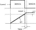
目前一种输出恒流的现有技术是通过在原边模拟出副边电流,将副边输出电流模拟出来或副边输出电流平均值计算出来,然后在原边进行恒流控制,如图3所示,通过对原边电流ipri进行采样保持以获取原边电流峰值及对应的副边电流峰值,其中ipri为原边电流信号,Vcontrol为采样信号,isample为采样保持模块输出信号,iemu为副边电流模拟模块输出信号。然而在实际电路中,由于采样保持模块在采样与保持切换之间存在一定的延时时间,会造成原边电流峰值采样的误差,从而造成模拟出的副边电流iemu与实际值存在偏差,如图4所示,并且该偏差值会随输入电压和变压器激磁电感量变化,比较难以补偿,从而造成输出恒流会随输入电压不同,变压器激磁电感不同而变化,输出恒流精度较低。At present, an existing technology for outputting constant current is to simulate the secondary side current on the primary side, simulate the secondary side output current or calculate the average value of the secondary side output current, and then perform constant current control on the primary side, as shown in Figure 3 , by sampling and holding the primary current ipri to obtain the peak value of the primary current and the corresponding peak value of the secondary current, where ipri is the primary current signal, Vcontrol is the sampling signal, isample is the output signal of the sampling and holding module, and iemu is the secondary current Analog block output signal. However, in the actual circuit, since there is a certain delay time between the sampling and holding switching of the sample-and-hold module, it will cause an error in the peak value sampling of the primary-side current, resulting in a deviation between the simulated secondary-side current iemu and the actual value, such as As shown in Figure 4, and the deviation value will vary with the input voltage and transformer excitation inductance, it is difficult to compensate, resulting in the output constant current will vary with the input voltage and transformer excitation inductance, and the output constant current accuracy is low.
另一种输出恒流常用的现有技术是恒功率的方法,如图5所示。交流输入信号经过整流后得到整流半波信号Vin,整流半波信号Vin经过电压前馈模块后得到交流输入电压的有效值,即输入电压前馈信号Vff;同时,其经过波形整形模块K1后得到波形信号Iac。其中,波形信号Iac=k×Vin,k为一系数。在恒流输出电路中Vea为可控常数。乘法器对所述波形信号Iac、输入电压前馈信号Vff和可控常数Vea进行乘法运算,得到正弦半波信号:Another common existing technology for outputting constant current is a constant power method, as shown in FIG. 5 . The rectified half-wave signal Vin is obtained after the AC input signal is rectified, and the effective value of the AC input voltage is obtained after the rectified half-wave signal Vin passes through the voltage feedforward module, that is, the input voltage feedforward signal Vff; at the same time, it is obtained after passing through the waveform shaping module K1 Waveform signal Iac. Wherein, the waveform signal Iac=k×Vin, k is a coefficient. Vea is a controllable constant in the constant current output circuit. The multiplier multiplies the waveform signal Iac, the input voltage feed-forward signal Vff and the controllable constant Vea to obtain a half-sine wave signal:
从而控制电感电流与正弦半波信号一致,实现PFC功能。可以看到,该乘法器通过将输入电压前馈信号的平方作为分子,在Vea一定的情况下,实现输入功率与输入电压无关,即恒功率控制。上述利用乘法器抵消输入电压的影响来获得电流基准的方法实质上为电压前馈控制。然而在有相控调光器存在的情况下,交流输入信号在调光角度不同时会缺失,其整流后也不再是完整的半波,因此输入前馈信号Vff包含了切相角度信号,该电压前馈控制会导致Iref随着切相角度的增加而急剧增加,输入功率也相应剧增,因此上述方法不适用于相控调光的场合。Therefore, the inductor current is controlled to be consistent with the half-sine wave signal, and the PFC function is realized. It can be seen that the multiplier uses the square of the input voltage feedforward signal as the numerator, and under the condition of a certain Vea, the input power is independent of the input voltage, that is, constant power control. The above method of using a multiplier to offset the influence of the input voltage to obtain the current reference is essentially a voltage feed-forward control. However, in the presence of a phase-controlled dimmer, the AC input signal will be missing when the dimming angle is different, and it will no longer be a complete half-wave after rectification, so the input feedforward signal Vff contains the phase-cut angle signal, The voltage feed-forward control will cause Iref to increase sharply with the increase of the phase-cut angle, and the input power will also increase sharply accordingly, so the above method is not suitable for the occasion of phase control dimming.
发明内容Contents of the invention
本发明克服上述现有技术中存在的缺陷,提出了一种电流基准发生电路,该电流基准发生电路能够产生自适应的开关电源主电路的原边电流信号跟随的基准信号提供给恒流开关电源控制电路,该基准信号可跟随电路输入输出条件变化进行自适应调整从而满足副边恒流输出的需要。The present invention overcomes the defects existing in the above-mentioned prior art, and proposes a current reference generating circuit, which can generate a reference signal followed by the primary current signal of the main circuit of an adaptive switching power supply and provide it to a constant current switching power supply The control circuit, the reference signal can be adaptively adjusted according to the change of the input and output conditions of the circuit so as to meet the needs of the constant current output of the secondary side.
同时本发明基于电流基准发生电路实现了一种原边控制的高功率恒流开关电源控制电路。At the same time, the present invention realizes a high-power constant-current switching power supply control circuit controlled by the primary side based on the current reference generating circuit.
电流基准发生电路包括:The current reference generation circuit consists of:
第一乘法器模块:所述第一乘法器模块接收来自开关电源主电路的整流桥输出的整流电压波形信号Iac和平均电流环输出的误差放大信号Vcomp,产生正弦半波信号Iref,所述正弦半波信号Iref与整流电压波形信号Iac同频同相,正弦半波信号Iref的幅值随误差放大信号Vcomp变化而变化,正弦半波信号Iref作为开关电源主电路的原边电流信号跟随的基准信号;The first multiplier module: the first multiplier module receives the rectified voltage waveform signal Iac output by the rectifier bridge of the main circuit of the switching power supply and the error amplification signal Vcomp output by the average current loop, and generates a sine half-wave signal Iref, the sine wave The half-wave signal Iref and the rectified voltage waveform signal Iac have the same frequency and phase. The amplitude of the sine half-wave signal Iref changes with the change of the error amplifier signal Vcomp. The sine half-wave signal Iref is used as the reference signal followed by the primary current signal of the main circuit of the switching power supply. ;
第二乘法器模块,所述第二乘法器模块输入所述正弦半波信号Iref和控制信号Vcontrol,产生第一脉冲信号iemu,所述控制信号Vcontrol是反映开关电源主电路输出二极管导通时间的脉冲信号,所述第一脉冲信号iemu的幅值包络线是与所述正弦半波信号Iref同频、同相且幅值成比例的正弦半波,第一脉冲信号iemu的脉冲宽度等于控制信号Vcontrol的脉冲宽度;The second multiplier module, the second multiplier module inputs the sine half-wave signal Iref and the control signal Vcontrol to generate the first pulse signal iemu, and the control signal Vcontrol reflects the conduction time of the output diode of the main circuit of the switching power supply Pulse signal, the amplitude envelope of the first pulse signal iemu is a half-sine wave with the same frequency and phase as the half-sine-wave signal Iref, and the amplitude is proportional, and the pulse width of the first pulse signal iemu is equal to the control signal The pulse width of Vcontrol;
平均电流环,所述平均电流环输入第一脉冲信号iemu和平均电流环基准信号Vref,所述第一脉冲信号iemu的平均值与设定的平均电流环基准信号Vref进行比较,二者之间的误差经平均电流环的补偿网络放大之后得到输出误差放大信号(Vcomp)。The average current loop, the average current loop inputs the first pulse signal iemu and the average current loop reference signal Vref, the average value of the first pulse signal iemu is compared with the set average current loop reference signal Vref, between the two After the error is amplified by the compensation network of the average current loop, the output error amplification signal (Vcomp) is obtained.
进一步,所述平均电流环具有滤波功能,对第一脉冲信号iemu进行滤波得到第一脉冲信号iemu的平均值。Further, the average current loop has a filtering function, and filters the first pulse signal iemu to obtain the average value of the first pulse signal iemu.
进一步,若所述平均电流环不具有滤波功能或要直接将iemu滤波后再送入平均电流环,所述电流基准发生电路还包括滤波器,所述滤波器对第一脉冲信号iemu进行滤波,滤除其高频谐波,得到第一脉冲信号iemu的平均值提供给平均电流环。Further, if the average current loop does not have a filter function or the iemu is to be directly filtered and then sent to the average current loop, the current reference generating circuit further includes a filter, the filter filters the first pulse signal iemu, and filters In addition to its high-frequency harmonics, the average value of the first pulse signal iemu is obtained and provided to the average current loop.
进一步,所述第一脉冲信号iemu波形反映两倍输出二极管电流波形,因此只要通过平均电流环控制第一脉冲信号iemu的平均值为常数的话,即可实现输出电流恒流。Further, the waveform of the first pulse signal iemu reflects twice the output diode current waveform, so as long as the average value of the first pulse signal iemu is controlled to be constant through the average current loop, the constant output current can be realized.
所述的开关电源主电路工作在电流断续或者临界断续状态。The main circuit of the switching power supply works in the state of current discontinuity or critical discontinuity.
所述的第二乘法器模块是乘法器或者实现等效功能的等效电路模块。The second multiplier module is a multiplier or an equivalent circuit module that realizes equivalent functions.
所述控制信号Vcontrol来自开关电源变压器的辅助绕组或者开关电源主电路的原边开关管的门极控制信号。The control signal Vcontrol comes from the auxiliary winding of the switching power supply transformer or the gate control signal of the primary switching tube of the switching power supply main circuit.
所述控制信号Vcontrol的幅值固定不变。The amplitude of the control signal Vcontrol is constant.
所述控制信号Vcontrol的正脉冲宽度与开关电源主电路的输出二极管导通时间相同。The positive pulse width of the control signal Vcontrol is the same as the conduction time of the output diode of the switching power supply main circuit.
所述的平均电流环包括误差放大器及补偿网络;The average current loop includes an error amplifier and a compensation network;
所述的平均电流环基准信号Vref是直流基准;The average current loop reference signal Vref is a DC reference;
所述的平均电流环基准信号Vref在相控调光时为能反映相控调光角的脉冲信号。The average current loop reference signal Vref is a pulse signal that can reflect the phase control dimming angle during phase control dimming.
一种原边控制的高功率因数恒流开关电源控制电路包括:电流基准发生电路、输出二极管导通时间检测模块、比较器、开关管导通控制模块和RS触发器:A high power factor constant current switching power supply control circuit controlled by the primary side includes: a current reference generation circuit, an output diode conduction time detection module, a comparator, a switch tube conduction control module and an RS trigger:
其中,所述电流基准发生电路如上所述;Wherein, the current reference generating circuit is as described above;
所述输出二极管导通时间检测模块检测开关电源主电路输出二极管的导通时间,输出控制信号Vcontrol给电流基准发生电路;The output diode conduction time detection module detects the conduction time of the switching power supply main circuit output diode, and outputs the control signal Vcontrol to the current reference generation circuit;
所述比较器的两个输入端分别输入电流基准发生电路输出的正弦半波信号Iref和原边电流信号采样值,并进行比较;当原边电流信号采样值上升到触及正弦半波信号Iref时,比较器输出信号从低电平翻转为高电平,此后当原边电流信号采样值下降到低于正弦半波信号Iref时,比较器输出信号从高电平翻转为低电平;The two input terminals of the comparator input the sine half-wave signal Iref output by the current reference generating circuit and the sampling value of the primary current signal respectively, and compare them; when the sampling value of the primary current signal rises to touch the sine half-wave signal Iref , the output signal of the comparator flips from low level to high level, and then when the sampling value of the primary current signal drops below the sine half-wave signal Iref, the output signal of the comparator flips from high level to low level;
所述RS触发器的两个输入端分别连接比较器的输出端和开关管导通控制模块,输出触发信号给主电路的原边开关管,比较器的输出端接RS触发器的复位端R端,开关管导通控制模块的输出接RS触发器的置位端S端;当RS触发器的复位端R端检测到一个从低电平到高电平的上升沿跳变时,RS触发器的输出信号从高电平复位为低电平,控制开关电源主电路的原边开关管的关断,当RS触发器的置位端S端检测到一个从低电平到高电平的上升沿跳变时,RS触发器的输出信号从低电平置位为高电平,如此周而复始,RS触发器输出脉冲序列信号。The two input ends of the RS flip-flop are respectively connected to the output end of the comparator and the switching tube conduction control module, and the trigger signal is output to the primary side switching tube of the main circuit, and the output end of the comparator is connected to the reset terminal R of the RS flip-flop. Terminal, the output of the switch conduction control module is connected to the set terminal S terminal of the RS flip-flop; when the reset terminal R terminal of the RS flip-flop detects a rising edge transition from low level to high level, the RS trigger The output signal of the device resets from high level to low level, and controls the switching off of the primary switch tube of the main circuit of the switching power supply. When the rising edge jumps, the output signal of the RS flip-flop is set from low level to high level, and so on, the RS flip-flop outputs a pulse train signal.
所述的开关管导通控制模块为定时触发器,所述的定时触发器产生频率固定的时钟信号提供给RS触发器的置位端S端,控制开关电源主电路的原边开关管的导通。The switching tube conduction control module is a timing trigger, and the timing trigger generates a clock signal with a fixed frequency and provides it to the setting terminal S of the RS flip-flop to control the conduction of the switching tube of the primary side of the main circuit of the switching power supply. Pass.
所述的开关管导通控制模块包括所述输出二极管导通时间检测模块、反相器和延时电路,通过检测输出二极管电流导通时间产生控制信号,然后加以反相和延时后提供给RS触发器的置位端S端,控制开关电源主电路的原边开关管的导通。The switch tube conduction control module includes the output diode conduction time detection module, an inverter and a delay circuit, and generates a control signal by detecting the output diode current conduction time, and then provides it to the The setting terminal S terminal of the RS flip-flop controls the conduction of the primary switching tube of the main circuit of the switching power supply.
恒流开关电源的控制方法,所述恒流开关电源包括如上所述的恒流开关电源控制电路,所述控制方法包括如下步骤:A control method for a constant current switching power supply, the constant current switching power supply includes the constant current switching power supply control circuit as described above, and the control method includes the following steps:
(1)使开关电源的主电路工作在电流断续或者临界断续状态;(1) Make the main circuit of the switching power supply work in an intermittent or critical intermittent state;
(2)检测开关电源主电路的整流桥输出的整流电压波形信号(Iac);(2) Detect the rectified voltage waveform signal (Iac) output by the rectifier bridge of the main circuit of the switching power supply;
(3)所述第一乘法器模块接收来自开关电源主电路的整流桥输出的整流电压波形信号(Iac)和平均电流环输出的误差放大信号(Vcomp),产生正弦半波信号(Iref),所述正弦半波信号(Iref)与整流电压波形信号(Iac)同频同相,正弦半波信号(Iref)的幅值随平均电流环输出的误差放大信号(Vcomp)变化而变化,正弦半波信号(Iref)作为开关电源主电路的原边电流信号跟随的基准信号;所述第二乘法器模块输入所述正弦半波信号(Iref)和控制信号(Vcontrol),产生第一脉冲信号(iemu),所述控制信号(Vcontrol)是反映开关电源主电路输出二极管导通时间的脉冲信号,所述第一脉冲信号(iemu)的幅值包络线是与所述正弦半波信号(Iref)同频、同相且幅值成比例的正弦半波,第一脉冲信号(iemu)的脉冲宽度等于控制信号(Vcontrol)的脉冲宽度;(3) The first multiplier module receives the rectified voltage waveform signal (Iac) output by the rectifier bridge of the switching power supply main circuit and the error amplification signal (Vcomp) output by the average current loop, and generates a half-sine wave signal (Iref), The sine half-wave signal (Iref) and the rectified voltage waveform signal (Iac) have the same frequency and phase, the amplitude of the sine half-wave signal (Iref) changes with the error amplification signal (Vcomp) output by the average current loop, and the sine half-wave The signal (Iref) is used as the reference signal followed by the primary current signal of the main circuit of the switching power supply; the second multiplier module inputs the half-sine wave signal (Iref) and the control signal (Vcontrol) to generate the first pulse signal (iemu ), the control signal (Vcontrol) is a pulse signal that reflects the conduction time of the output diode of the switching power supply main circuit, and the amplitude envelope of the first pulse signal (iemu) is the same as the half-sine wave signal (Iref) Sine half wave with the same frequency, same phase and proportional amplitude, the pulse width of the first pulse signal (iemu) is equal to the pulse width of the control signal (Vcontrol);
所述平均电流环输入第一脉冲信号(iemu)和平均电流环基准信号(Vref),所述第一脉冲信号(iemu)的平均值与设定的平均电流环基准信号(Vref)进行比较,二者之间的误差经平均电流环的补偿网络放大之后输出误差放大信号(Vcomp);The average current loop inputs the first pulse signal (iemu) and the average current loop reference signal (Vref), and the average value of the first pulse signal (iemu) is compared with the set average current loop reference signal (Vref), The error between the two is amplified by the compensation network of the average current loop and then the error amplification signal (Vcomp) is output;
(4)根据步骤(3)得到的正弦半波信号(Iref)以及原边电流信号采样值,产生开关电源主电路的原边开关管驱动脉冲的关断信号;(4) According to the sinusoidal half-wave signal (Iref) obtained in step (3) and the sampled value of the primary current signal, a turn-off signal of the driving pulse of the primary switching tube of the main circuit of the switching power supply is generated;
(5)产生原边开关管驱动脉冲的导通信号;(5) Generate the conduction signal of the driving pulse of the primary switching tube;
(6)重复步骤(1)-(5)。(6) Repeat steps (1)-(5).
本发明的有益效果为:The beneficial effects of the present invention are:
本发明提出的一种电流基准发生电路的第二乘法器的输出信号iemu与图3采用采样保持模块和副边电流模拟模块模拟出的电流波形不同,虽然二者的正脉宽都为输出二极管的导通时间,但是iemu的每个脉冲波形的高电平都是正弦半波的包络线,而图3中模拟出的脉冲电流波形的高电平是采样保持模块输出的水平直线。该电流基准发生电路能够产生自适应的开关电源主电路的原边电流信号跟随的基准信号提供给恒流开关电源控制电路,该基准信号可跟随电路输入输出条件变化进行自适应调整从而满足副边恒流输出的需要。The output signal iemu of the second multiplier of a current reference generation circuit proposed by the present invention is different from the current waveform simulated by the sample-and-hold module and the secondary current simulation module in Fig. The conduction time, but the high level of each pulse waveform of iemu is the envelope of the half-sine wave, while the high level of the pulse current waveform simulated in Figure 3 is the horizontal straight line output by the sample and hold module. The current reference generation circuit can generate an adaptive switching power supply main circuit. The reference signal followed by the primary side current signal is provided to the constant current switching power supply control circuit. The need for constant current output.
本发明提出的恒流开关电源控制电路的输出恒流控制是一种自适应的负反馈闭环控制方式,即产生的正弦半波信号的幅值受到平均电流环控制,而产生的正弦半波信号又会影响到平均电流环的输入信号从而影响到平均电流环的输出。当开关电源外部条件发生变化,如输入电压改变或输出电压改变,平均电流环的输出发生改变,从而改变正弦半波信号幅值,经过负反馈达到平衡之后重新实现输出恒流;通过将原边电流对产生正弦半波信号进行跟随,可以实现高功率因数。本发明提出的恒流开关电源控制电路及方法无需对原边电流进行采样保持,消除了采样保持带来的误差,提高了输出电流的恒流精度,此外与电压前馈的恒功率方法相比,本发明产生的是一种自适应的电流基准,恒流精度不受乘法器影响,在相控调光时电流基准可直接由切相角获得而无需经过乘法器,因此输入功率不受切相角度影响,无需增加额外的控制成本。此外,本发明的恒流开关电源控制电路可集成为单芯片。The output constant current control of the constant current switching power supply control circuit proposed by the present invention is an adaptive negative feedback closed-loop control method, that is, the amplitude of the generated half-sine wave signal is controlled by the average current loop, and the half-sine wave signal generated It will also affect the input signal of the average current loop and thus affect the output of the average current loop. When the external conditions of the switching power supply change, such as the input voltage changes or the output voltage changes, the output of the average current loop changes, thereby changing the amplitude of the half-sine wave signal, and re-realizes the output constant current after reaching balance through negative feedback; The current follows the sinusoidal half-wave signal to achieve high power factor. The constant current switching power supply control circuit and method proposed by the present invention do not need to sample and hold the primary current, eliminate the error caused by sampling and holding, and improve the constant current accuracy of the output current. In addition, compared with the constant power method of voltage feedforward , the present invention produces an adaptive current reference, the constant current accuracy is not affected by the multiplier, and the current reference can be directly obtained from the phase cut angle without going through the multiplier during phase control dimming, so the input power is not affected by the cut Phase angle influence, no need to add additional control costs. In addition, the constant current switching power supply control circuit of the present invention can be integrated into a single chip.
附图说明Description of drawings
图1为现有技术中的一种副边恒流的单级功率因数校正电路;Fig. 1 is a single-stage power factor correction circuit of secondary side constant current in the prior art;
图2为原边控制的具有高功率因数的恒流电路示意图;Fig. 2 is a schematic diagram of a constant current circuit with high power factor controlled by the primary side;
图3为一种现有技术的原边控制的恒流开关电源及其控制电路;Fig. 3 is a kind of constant current switching power supply and its control circuit of primary side control of prior art;
图4为采样保持电路造成的采样误差示意图;Fig. 4 is a schematic diagram of the sampling error caused by the sample and hold circuit;
图5为基于恒功率原理实现的原边控制的恒流输出PFC电路;Figure 5 is a constant current output PFC circuit based on the principle of constant power to achieve the primary side control;
图6A、图6B为本发明的电流基准发生电路;Fig. 6A, Fig. 6B are the electric current reference generation circuit of the present invention;
图7为本发明的电流基准发生电路一个具体实施例;Fig. 7 is a specific embodiment of the current reference generation circuit of the present invention;
图8为图6A和图6B电路的关键波形示意图;Fig. 8 is a schematic diagram of key waveforms of the circuits of Fig. 6A and Fig. 6B;
图9为本发明的电流基准发生电路构成的原边控制的定频高功率因数控制电路应用于反激式恒流开关电源的一个具体实施例;Fig. 9 is a specific embodiment of a flyback constant current switching power supply applied to a primary side controlled fixed frequency high power factor control circuit composed of a current reference generating circuit of the present invention;
图10为图9所示电路中的输出二极管导通时间检测模块的一个具体实施例;Fig. 10 is a specific embodiment of the output diode conduction time detection module in the circuit shown in Fig. 9;
图11为图10电路的关键波形示意图;Fig. 11 is a schematic diagram of key waveforms of the circuit in Fig. 10;
图12为图9所示实施例电路的关键波形;Fig. 12 is the key waveform of the embodiment circuit shown in Fig. 9;
图13为本发明的电流基准发生电路100构成的原边控制的变频高功率因数控制电路应用于反激式恒流开关电源的一个具体实施例;Fig. 13 is a specific embodiment of a flyback constant current switching power supply applied to a primary-side controlled frequency conversion high power factor control circuit composed of a current
图14为图13所示电路的关键波形;Fig. 14 is the key waveform of the circuit shown in Fig. 13;
图15为图13所示实施例电路在半个交流输入工频周期内的归一化的输出电流计算波形;Fig. 15 is the normalized output current calculation waveform of the embodiment circuit shown in Fig. 13 in half of the AC input power frequency cycle;
图16为本发明应用于定频高功率因数非隔离型buck-boost型(升降压)恒流开关电源的一个具体实施例;Figure 16 is a specific embodiment of the present invention applied to a fixed-frequency high power factor non-isolated buck-boost (boost-boost) constant-current switching power supply;
图17为本发明应用于变频高功率因数非隔离型buck-boost型(升降压)恒流开关电源的一个具体实施例。Fig. 17 is a specific embodiment of the present invention applied to a non-isolated buck-boost (buck-boost) constant-current switching power supply with variable frequency and high power factor.
图18是本发明与可控硅调光电路结合起来实现的可调光原边控制的高功率因素反激式恒流开关电源。Fig. 18 is a high power factor flyback constant current switching power supply with dimmable primary side control realized by combining the present invention with a thyristor dimming circuit.
具体实施方式Detailed ways
以下结合本发明框图以及具体实施例示意图本发明内容进行详细说明。The content of the present invention will be described in detail below in conjunction with the block diagram of the present invention and the schematic diagrams of specific embodiments.
如图6A所示,本发明的电流基准发生电路100包括:As shown in FIG. 6A, the current
第一乘法器模块101:所述第一乘法器模块101接收来自开关电源主电路的整流桥输出的整流电压波形信号Iac和平均电流环104输出的误差放大信号Vcomp,产生正弦半波信号Iref,所述正弦半波信号Iref同整流电压波形信号Iac同频同相,正弦半波信号Iref的幅值随误差放大信号Vcomp变化而变化,正弦半波信号Iref作为开关电源主电路的原边电流信号跟随的基准信号;The first multiplier module 101: the
第二乘法器模块102,所述第二乘法器模块102输入所述正弦半波信号Iref和控制信号Vcontrol,产生第一脉冲信号iemu,所述控制信号Vcontrol是反映开关电源主电路输出二极管导通时间的脉冲信号,所述第一脉冲信号iemu的幅值包络线是与所述正弦半波信号Iref同频、同相且幅值成比例的正弦半波,第一脉冲信号iemu的脉冲宽度等于控制信号Vcontrol的脉冲宽度;The
平均电流环104,所述平均电流环104输入第一脉冲信号iemu和平均电流环基准信号Vref,所述第一脉冲信号iemu的平均值与设定的平均电流环基准信号Vref进行比较,输出信号误差放大信号Vcomp。The average
进一步,所述平均电流环104具有一定的滤波功能,对第一脉冲信号iemu进行滤波得到第一脉冲信号iemu的平均值。Further, the average
进一步,若所述平均电流环104不具有滤波功能或要直接将iemu滤波后送入平均电流环,所述电流基准发生电路100还包括滤波器103,如图6B,所述滤波器对第一脉冲信号iemu进行滤波,滤除其高频谐波,得到第一脉冲信号iemu的平均值提供给平均电流环。Further, if the average
进一步,所述第一脉冲信号iemu波形反映两倍输出二极管电流波形、幅值反映原边电流信号幅值,因此只要通过平均电流环控制第一脉冲信号iemu的平均值为常数的话,即可实现输出电流恒流。Further, the waveform of the first pulse signal iemu reflects twice the output diode current waveform, and the amplitude reflects the amplitude of the primary current signal, so as long as the average value of the first pulse signal iemu is controlled to be a constant through the average current loop, it can be realized The output current is constant.
所述的开关电源主电路工作在电流断续或者临界断续状态。The main circuit of the switching power supply works in the state of current discontinuity or critical discontinuity.
所述的第二乘法器模块102是乘法器或者实现等效功能的等效电路模块,如图7所示。The
所述控制信号Vcontrol来自开关电源变压器的辅助绕组或者开关电源主电路的原边开关管的门极控制信号。The control signal Vcontrol comes from the auxiliary winding of the switching power supply transformer or the gate control signal of the primary switching tube of the switching power supply main circuit.
所述控制信号Vcontrol的幅值固定不变。The amplitude of the control signal Vcontrol is constant.
所述控制信号Vcontrol的正脉冲宽度与开关电源主电路的输出二极管导通时间相同。The positive pulse width of the control signal Vcontrol is the same as the conduction time of the output diode of the switching power supply main circuit.
所述的平均电流环包括误差放大器及补偿网络,如图7所示。The average current loop includes an error amplifier and a compensation network, as shown in FIG. 7 .
所述的平均电流环基准信号Vref是直流基准;The average current loop reference signal Vref is a DC reference;
所述的平均电流环基准信号Vref在相控调光时为能反映相控调光角的脉冲信号,如图7所示。The average current loop reference signal Vref is a pulse signal that can reflect the phase control dimming angle during phase control dimming, as shown in FIG. 7 .
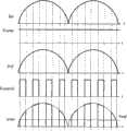
图8为图6电路中主要关键波形,其中Iac为开关电源主电路的整流桥输出的整流电压波形信号,Vcomp为平均电流环104输出的误差放大信号,Iref是第一乘法器101输出的正弦半波信号,Vcontrol是反映开关电源主电路输出二极管导通时间的控制信号,iemu是第二乘法器的输出的第一脉冲信号,Vref是平均电流环基准信号。Fig. 8 is the main key waveform in the circuit of Fig. 6, wherein Iac is the rectified voltage waveform signal output by the rectifier bridge of the switching power supply main circuit, Vcomp is the error amplification signal output by the average
图9是本发明的电流基准发生电路构成的原边控制的定频高功率因数恒流开关电源控制电路应用于反激式恒流开关电源的一个具体实施例,其中反激式开关电源工作在断续模式。Fig. 9 is a specific embodiment of a flyback constant current switching power supply with a fixed frequency high power factor constant current switching power supply control circuit composed of the current reference generation circuit of the present invention, where the flyback switching power supply works in intermittent mode.
开关电源包括:主电路和原边控制的恒流开关电源的控制电路,其中,所述主电路包括交流输入10、整流桥11、输入电容12、整流桥电压波形采样电路13、变压器14、原边开关管15、采样电阻16、输出二极管17和输出电容18;其中,所述控制电路包括电流基准发生电路100、输出二极管导通时间检测模块200、平均电流环基准300、比较器400、定时触发器500和RS触发器600,以及原边电流采样端、输出二极管导通时间检测端、整流桥电压波形信号检测端和驱动端;The switching power supply includes: a main circuit and a control circuit of a constant current switching power supply controlled by the primary side, wherein the main circuit includes an
原边控制的恒流开关电源的控制电路的连接关系如下:输出二极管导通时间检测模块200的一个输入端I1接输出二极管导通时间检测端,输出二极管导通时间检测模块的另一个输入端I2接RS触发器600的输出端Q,输出二极管导通时间检测模块200的输出端O1接电流基准发生电路100的Vcontrol端,比较器400的负输入端接电流基准发生电路100的输出Iref端,比较器400的正输入端接原边电流采样端,比较器400的输出接RS触发器600的R端(复位端),定时触发器500的输出接RS触发器600的S端(置位端),RS触发器600的输出Q接驱动端,电流基准发生电路100的Iac端接整流桥电压波形信号检测端,电流基准发生电路100内部模块连接如前文所述,电流基准发生电路100的Vref端接平均电流环基准300。The connection relationship of the control circuit of the constant current switching power supply controlled by the primary side is as follows: an input terminal I1 of the output diode conduction time detection module 200 is connected to the output diode conduction time detection terminal, and the other input terminal of the output diode conduction time detection module I2 is connected to the output terminal Q of the RS flip-flop 600, the output terminal O1 of the output diode conduction time detection module 200 is connected to the Vcontrol terminal of the current reference generating circuit 100, and the negative input terminal of the comparator 400 is connected to the output Iref terminal of the current reference generating circuit 100 , the positive input terminal of the comparator 400 is connected to the primary current sampling terminal, the output of the comparator 400 is connected to the R terminal (reset terminal) of the RS flip-flop 600 , the output of the timing flip-flop 500 is connected to the S terminal of the RS flip-flop 600 (set terminal), the output Q of the RS flip-flop 600 is connected to the drive terminal, the Iac terminal of the current reference generating circuit 100 is connected to the rectifier bridge voltage waveform signal detection end, and the internal modules of the current reference generating circuit 100 are connected as described above, the current reference generating circuit 100 Vref is terminated with an average current loop reference 300 .
主电路的连接关系如下:交流输入10两端接整流桥11的两个输入端,整流桥11的正输出端接输入电容12的一端、整流桥电压波形采样电路13的一端和变压器14原边绕组的同名端,整流桥11的负输出端接地,输入电容12的另一端接地,整流桥电压波形采样电路13的另一端接控制电路的整流桥电压波形信号检测端,变压器14的原边绕组的异名端接原边开关管15的漏极,原边开关管15的源极接采样电阻16的一端和控制电路的原边电流采样端,采样电阻16的另一端接地,变压器14的副边绕组的异名端接输出二极管17的阳极,输出二极管17的阴极接输出电容18的正极,变压器14的副边绕组的同名端和输出电容18的负极相连,变压器14的辅助绕组的同名端接地,变压器14的辅助绕组的异名端接控制电路的输出二极管导通时间检测端,原边开关管15的门极接控制电路的驱动端。The connection relationship of the main circuit is as follows: the two ends of the
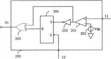
图10为输出二极管导通时间检测模块200的一个具体实施例,包括比较器201、偏置基准202、反相器203、RS触发器204和异或门205。其中比较器201的正输入端接输出二极管导通时间检测模块200的一个输入端I1,比较器201的负输入端接偏置基准202,比较器201的输出端接反相器203的输入端,反相器203的输出端分别接RS触发器204的R端(复位端)和异或门205的一个输入端,RS触发器204的S端(置位端)接输出二极管导通时间检测模块200的另一个输入端I2,RS触发器204的输出端Q接输出二极管导通时间检测模块200的输出端O1。图10所示输出二极管导通时间检测模块200实施例的关键波形如图11所示,其中VI1是输入端I1的波形信号,图中所示为输入端I1接主电路辅助绕组异名端时的波形;V201为比较器201的输出波形信号;V203为反相器203的输出波形信号;VI2为输入端200的输入信号,与主电路原边开关管门极驱动信号相同;V204为RS触发器204的输出波形信号;VO1为异或门205的输出信号。从图11所示波形可以看出,图10所示输出二极管导通时间检测模块可以检测出主电路辅助绕组异名端高电平的区间,从而大致检测出主电路输出二极管导通时间区间。FIG. 10 is a specific embodiment of an output diode conduction
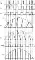
图9所示电路的关键波形如图12所示,其中,V400为比较器300的输出波形,为原边开关管15驱动脉冲的复位信号;V500是定时触发器500的输出波形,为原边开关管15驱动脉冲的置位信号;V600是RS触发器600的输出波形,即原边开关管15驱动脉冲信号;ipri为主电路原边电流波形;isec为主电路输出二极管电流波形;Iref是第一乘法器101的输出波形;Vcontrol为输出二极管导通时间检测模块200的输出波形,iemu是第二乘法器102的输出波形;电路主要工作原理如下:(1)通过整流桥11输出电压采样电路13得到开关电源主电路的整流桥输出电压的波形信号Iac;(2)通过输出二极管导通时间检测模块200检测变压器14的辅助绕组的正电平区间得到输出二极管导通时间信号Vcontrol;(3)将上述两个信号Iac和Vcontrol送入本发明的原边控制的恒流开关电源原边电流基准发生电路100,产生自适应的原边正弦半波信号Iref;(4)采样电阻16上的原边电流与电流基准Iref通过比较器400进行比较产生原边驱动信号的复位信号,即当采样电阻16上的原边电流上升到电流基准Iref幅值时,比较器400的输出信号从低电平置位高电平,该跳变信号送入到RS触发器400的复位端,将RS触发器600产生的输出脉冲进行复位;(5)定时触发器500产生的窄脉冲上升沿对RS触发器600产生的输出脉冲进行置位,因此输出脉冲为频率固定的脉冲信号。由之前的描述可知,当开关电源主电路输入或输出条件发生变化时,通过平均电流环可自动调节原边正弦半波信号Iref使输出电流保持不变从而实现输出恒流;假设输入电压为Vac=Vpksinωt,Iref=Ipk|sinωt|,则可得到开关电源的占空比为:The key waveform of the circuit shown in Fig. 9 is shown in Fig. 12, wherein, V400 is the output waveform of the comparator 300, which is the reset signal of the drive pulse of the switching tube 15 on the primary side; V500 is the output waveform of the timing flip-flop 500, which is the The setting signal of the driving pulse of the switching tube 15; V600 is the output waveform of the RS flip-flop 600, that is, the driving pulse signal of the switching tube 15 on the primary side; ipri is the primary current waveform of the main circuit; isec is the output diode current waveform of the main circuit; Iref is The output waveform of the first multiplier 101; Vcontrol is the output waveform of the output diode conduction time detection module 200, and iemu is the output waveform of the second multiplier 102; the main working principle of the circuit is as follows: (1) sampling the output voltage through the rectifier bridge 11 The circuit 13 obtains the waveform signal Iac of the output voltage of the rectifier bridge of the main circuit of the switching power supply; (2) the output diode conduction time signal Vcontrol is obtained by detecting the positive level interval of the auxiliary winding of the transformer 14 through the output diode conduction time detection module 200; ( 3) Send the above two signals Iac and Vcontrol into the primary side current reference generation circuit 100 of the primary side controlled constant current switching power supply of the present invention to generate an adaptive primary side sine half-wave signal Iref; (4) Sampling resistor 16 The primary current of the original side is compared with the current reference Iref by the comparator 400 to generate the reset signal of the primary side drive signal, that is, when the primary current on the sampling resistor 16 rises to the amplitude of the current reference Iref, the output signal of the comparator 400 changes from low to low. The level is set to a high level, and the jump signal is sent to the reset terminal of the RS flip-
其中Lm是变压器14的激磁电感量,f是开关电源的工作频率,即RS触发器600的输出脉冲频率,ω是输入交流电压角频率,ω=2πfline,fline是输入交流电压频率,由式(1)可知,在特定的输入电压和输出电流情况下,占空比D为常数,进一步可以求出输入交流电流的平均值为:Where Lm is the magnetizing inductance of the
由式(2)可知,开关电源交流输入电流波形为纯正弦,因此可以获得非常高的功率因数。图13是基于本发明的电流基准发生电路100构成的原边控制的变频高功率因数控制电路应用于反激式恒流开关电源的一个具体实施例,其中反激式开关电源工作在临界断续模式,即准谐振模式;控制电路包括平均电流基准000、本发明的电流基准发生电路100、输出二极管导通时间检测模块600、比较器700、反相器模块800和RS触发器900,以及原边电流采样端、输出二极管导通时间检测端、整流桥电压波形信号检测端和驱动端;主电路包括交流输入10、整流桥11、输入电容12、整流桥电压波形采样电路13、变压器14、原边开关管15、采样电阻16、输出二极管17和输出电容18;其中控制电路的连接关系如下:输出二极管导通时间检测模块600包括比较器601和比较器基准602,比较器601的正输入端接输出二极管导通时间检测端,比较器601的负输入端接比较器基准602的一端,比较器基准602的另一端接地,比较器601的输出作为输出二极管导通时间检测模块600的输出接电流基准发生电路100的Vcontrol端和反相器模块800的输入端,比较器700的正输入端接原边电流采样端,比较器700的负输入端接电流基准发生电路100的Iref端,比较器700的输出接RS触发器900的R端(复位端),电流基准发生电路100的Iac端接整流桥电压波形信号检测端,反相器模块800包括反相器801和延时环节802,反相器801的输入端即为反相器模块800的输入端,反相器801的输出端接延时环节802的输入端,延时环节802的输出端即为反相器模块800的输出端,反相器模块800的输出接RS触发器900的S端(置位端),RS触发器900的输出Q接驱动端,电流基准发生电路100的Vref端接平均电流环基准000。主电路连接关系如下:交流输入10两端接整流桥11的两个输入端,整流桥11的正输出端接输入电容11的一端、整流桥电压波形采样电路13的一端和变压器14原边绕组的同名端,整流桥11的负输出端接地,输入电容11的另一端接地,整流桥电压波形采样电路13的另一端接控制电路的整流桥电压波形信号检测端,变压器14的原边绕组的异名端接原边开关管15的漏极,原边开关管15的源极接采样电阻16的一端和控制电路的原边电流采样端,采样电阻16的另一端接地,变压器14的副边绕组的异名端接输出二极管17的阳极,输出二极管17的阴极接输出电容18的正极,变压器14的副边绕组的同名端和输出电容18的负极相连,变压器14的辅助绕组的同名端接地,变压器14的辅助绕组的异名端接控制电路的输出二极管导通时间检测端。It can be seen from formula (2) that the AC input current waveform of the switching power supply is pure sine, so a very high power factor can be obtained. Fig. 13 is a specific embodiment of a flyback constant current switching power supply based on a primary-side controlled frequency conversion high power factor control circuit composed of a current reference generating circuit 100 of the present invention, wherein the flyback switching power supply operates at critical intermittent mode, that is, quasi-resonant mode; the control circuit includes an average current reference 000, a current reference generation circuit 100 of the present invention, an output diode conduction time detection module 600, a comparator 700, an inverter module 800 and an RS flip-flop 900, and the original Side current sampling terminal, output diode conduction time detection terminal, rectifier bridge voltage waveform signal detection terminal and drive terminal; the main circuit includes AC input 10, rectifier bridge 11, input capacitor 12, rectifier bridge voltage waveform sampling circuit 13, transformer 14, Primary switch tube 15, sampling resistor 16, output diode 17, and output capacitor 18; wherein the connection relationship of the control circuit is as follows: the output diode conduction time detection module 600 includes a comparator 601 and a comparator reference 602, and the positive input of the comparator 601 The terminal is connected to the output diode conduction time detection terminal, the negative input terminal of the comparator 601 is connected to one end of the comparator reference 602, and the other end of the comparator reference 602 is grounded, and the output of the comparator 601 is used as the output of the output diode conduction time detection module 600 Connect the Vcontrol end of the current reference generation circuit 100 and the input end of the inverter module 800, the positive input end of the comparator 700 is connected to the primary current sampling end, the negative input end of the comparator 700 is connected to the Iref end of the current reference generation circuit 100, The output of the comparator 700 is connected to the R terminal (reset terminal) of the RS flip-flop 900, the Iac terminal of the current reference generating circuit 100 is connected to the rectifier bridge voltage waveform signal detection terminal, and the inverter module 800 includes an inverter 801 and a delay link 802 , the input end of the inverter 801 is the input end of the inverter module 800, the output end of the inverter 801 is connected to the input end of the delay link 802, and the output end of the delay link 802 is the input end of the inverter module 800 At the output terminal, the output of the inverter module 800 is connected to the S terminal (set terminal) of the RS flip-flop 900 , the output Q of the RS flip-flop 900 is connected to the driving terminal, and the Vref terminal of the current reference generating circuit 100 is connected to the average current loop reference 000. The connection relationship of the main circuit is as follows: the two ends of the AC input 10 are connected to the two input terminals of the rectifier bridge 11, the positive output terminal of the rectifier bridge 11 is connected to one end of the input capacitor 11, one end of the rectifier bridge voltage waveform sampling circuit 13 and the primary winding of the transformer 14 The end of the same name of the rectifier bridge 11, the negative output terminal of the rectifier bridge 11 is grounded, the other end of the input capacitor 11 is grounded, the other end of the rectifier bridge voltage waveform sampling circuit 13 is connected to the rectifier bridge voltage waveform signal detection end of the control circuit, and the primary side winding of the transformer 14 The different terminal is connected to the drain of the primary switching tube 15, the source of the primary switching tube 15 is connected to one end of the sampling resistor 16 and the primary current sampling end of the control circuit, the other end of the sampling resistor 16 is grounded, and the secondary side of the transformer 14 The opposite end of the winding is connected to the anode of the output diode 17, the cathode of the output diode 17 is connected to the positive pole of the output capacitor 18, the same end of the secondary winding of the transformer 14 is connected to the negative end of the output capacitor 18, and the same end of the auxiliary winding of the transformer 14 is grounded , the differential terminal of the auxiliary winding of the transformer 14 is connected to the output diode conduction time detection terminal of the control circuit.
图13所示电路的关键波形如图14所示,其中,V700为比较器700的输出波形,为原边开关管15驱动脉冲的复位信号;V800是反相器模块800的输出波形,为原边开关管15驱动脉冲的置位信号;V900是RS触发器900的输出波形,即原边开关管15驱动脉冲信号;ipri为主电路原边电流波形;isec为主电路输出二极管电流波形;Iref是第一乘法器101的输出波形;Vcontrol为输出二极管导通时间检测模块600的输出波形,iemu是第二乘法器102的输出波形;电路主要工作原理如下:(1)通过整流桥11输出电压采样电路13得到开关电源主电路的整流桥输出电压的波形信号Iac;(2)通过输出二极管导通时间检测模块200检测变压器14的辅助绕组的正电平区间得到输出二极管导通时间信号Vcontrol;(3)将上述两个信号Iac和Vcontrol送入本发明的原边控制的恒流开关电源原边电流基准发生电路100,产生自适应的原边正弦半波信号Iref;(4)采样电阻16上的原边电流与电流基准Iref通过比较器300进行比较产生原边驱动信号的复位信号,即当采样电阻16上的原边电流上升到电流基准Iref幅值时,比较器700的输出信号从低电平置位高电平,该跳变信号送入到RS触发器900的复位端,将RS触发器900产生的输出脉冲进行复位;(5)通过检测变压器14辅助绕组电压的过零点检测出输出二极管电流波形的过零点,加以延时环节,产生让RS触发器900的输出脉冲置位的信号,从而实现原边开关管15谷底开通,即电路工作在准谐振模式,因此原边开关管15的驱动脉冲为变频脉冲信号。在图13所示实施例中,主电路输入电流绝对值表达式为:The key waveform of the circuit shown in Figure 13 is shown in Figure 14, wherein, V700 is the output waveform of the comparator 700, which is the reset signal of the driving pulse of the primary switch tube 15; V800 is the output waveform of the inverter module 800, which is the original The setting signal of the driving pulse of the side switch tube 15; V900 is the output waveform of the RS flip-flop 900, that is, the driving pulse signal of the primary side switching tube 15; the primary current waveform of the main circuit of ipri; the output diode current waveform of the main circuit of isec; Iref is the output waveform of the first multiplier 101; Vcontrol is the output waveform of the output diode conduction time detection module 600, and iemu is the output waveform of the second multiplier 102; the main working principle of the circuit is as follows: (1) Output voltage through the rectifier bridge 11 The sampling circuit 13 obtains the waveform signal Iac of the rectifier bridge output voltage of the switching power supply main circuit; (2) the output diode conduction time signal Vcontrol is obtained by detecting the positive level interval of the auxiliary winding of the transformer 14 through the output diode conduction time detection module 200; (3) Send the above two signals Iac and Vcontrol into the primary side current reference generating circuit 100 of the constant current switching power supply of the present invention to generate an adaptive primary side sine half-wave signal Iref; (4) Sampling resistor 16 The primary current on the sampling resistor 16 is compared with the current reference Iref by the comparator 300 to generate the reset signal of the primary drive signal, that is, when the primary current on the sampling resistor 16 rises to the amplitude of the current reference Iref, the output signal of the comparator 700 changes from The low level sets the high level, and the jump signal is sent to the reset terminal of the RS flip-flop 900 to reset the output pulse generated by the RS flip-flop 900; (5) By detecting the zero-crossing point detection of the auxiliary winding voltage of the transformer 14 The zero-crossing point of the output diode current waveform is added, and a delay link is added to generate a signal for setting the output pulse of the RS flip-flop 900, thereby realizing the opening of the primary side switch tube 15 at the bottom, that is, the circuit works in a quasi-resonant mode, so the primary side switch The driving pulse of the tube 15 is a variable frequency pulse signal. In the embodiment shown in Figure 13, the expression of the absolute value of the input current of the main circuit is:
其中Vo'为输出电压折算到变压器原边之后的电压,k为电流电压对应系数,D为占空比,为导通时间与开关周期的比值;Ipk是主电路原边电流峰值,Vpk是交流输入电压峰值;根据式(3)得到半个交流输入工频周期内的归一化的输出电流波形如图15所示,其中s=Vo’/Vac,可以看到交流输入电流波形接近正弦波;但随着s变小,即输入电压幅值增大,输入电流的波形失真越厉害,功率因数越低。Among them, Vo 'is the voltage converted from the output voltage to the primary side of the transformer, k is the corresponding coefficient of current and voltage, D is the duty cycle, and is the ratio of the conduction time to the switching period; Ipk is the peak current value of the primary side of the main circuit, and Vpk is The peak value of the AC input voltage; according to formula (3), the normalized output current waveform within half the AC input power frequency cycle is shown in Figure 15, where s=Vo '/Vac , and the AC input current waveform can be seen It is close to a sine wave; but as s becomes smaller, that is, the input voltage amplitude increases, the waveform distortion of the input current is more severe, and the power factor is lower.
本发明可以用于图9和图13所示的隔离型拓扑,也可用于非隔离型拓扑。图16是本发明应用于定频高功率因数非隔离型buck-boost型(升降压)恒流开关电源的一个具体实施例,其中控制电路与图9所示实施例完全相同,主电路与图9所示实施例区别在于图16中用电感14替代了图6中的变压器14,具体工作原理也与图9实施例相同;图17是本发明应用于变频高功率因数非隔离型buck-boost型(升降压)恒流开关电源的一个具体实施例,其中控制电路与图13所示实施例完全相同,主电路与图13所示实施例区别在于图17中用电感14替代了图13中的变压器14,具体工作原理也与图13实施例相同。The present invention can be used in the isolated topology shown in Fig. 9 and Fig. 13, and can also be used in the non-isolated topology. Figure 16 is a specific embodiment of the present invention applied to a fixed-frequency high power factor non-isolated buck-boost type (boost-boost) constant-current switching power supply, wherein the control circuit is exactly the same as the embodiment shown in Figure 9, and the main circuit is the same as The difference of the embodiment shown in Fig. 9 is that the
图18是本发明与可控硅调光电路结合起来实现的可调光原边控制的高功率因素反激式恒流开关电源。其中主要连接关系图与图9所示实施例大致相同,区别在于图18中主电路的交流输入10与整流桥11之间插入了可控硅调光器,控制电路中用切相角检测电路301替代了图9中的平均电流环基准300,用开关管导通控制模块501替代了图9中的定时触发器;切相角检测电路301的输入端接整流桥电压波形信号整流桥电压波形信号检测端,切相角检测电路301的输出端接电流基准发生电路100的Vref端;调光时,切相角检测电路301检测整流桥电压波形信号检测端的切相角信号,转换为幅值一定、占空比反映切相角的脉冲信号,送入电流基准发生电路100充当平均电流环的基准,从而可以改变输出电流的大小实现调光;开关管导通控制模块501用来控制原边开关管的开通,在图9中为定时触发器500,在图13中包括输出二极管导通时间检测模块600和反相器模块800。Fig. 18 is a high power factor flyback constant current switching power supply with dimmable primary side control realized by combining the present invention with a thyristor dimming circuit. The main connection diagram is roughly the same as the embodiment shown in Fig. 9, the difference is that in Fig. 18 a thyristor dimmer is inserted between the AC input 10 of the main circuit and the rectifier bridge 11, and a phase-cut angle detection circuit is used in the control circuit 301 replaces the average current loop reference 300 in Fig. 9, and replaces the timing trigger in Fig. 9 with the switching tube conduction control module 501; the input terminal of the phase-cut angle detection circuit 301 is connected to the rectifier bridge voltage waveform signal rectifier bridge voltage waveform Signal detection terminal, the output terminal of the phase-cut angle detection circuit 301 is connected to the Vref terminal of the current reference generation circuit 100; during dimming, the phase-cut angle detection circuit 301 detects the phase-cut angle signal of the voltage waveform signal detection terminal of the rectifier bridge, and converts it into an amplitude A pulse signal whose duty cycle reflects the phase-cut angle is sent to the current reference generating circuit 100 as the reference of the average current loop, so that the magnitude of the output current can be changed to realize dimming; the switching tube conduction control module 501 is used to control the primary side The turn-on of the switch tube is a timing flip-flop 500 in FIG. 9 , and includes an output diode conduction time detection module 600 and an inverter module 800 in FIG. 13 .
本发明包括的具体模块乘法器模块和平均电流环等,本领域技术人员可以在不违背其精神的前提下,可以有多种实施方式,或通过各种不同的组合方式,形成不同的具体实施例,例如乘法器模块可以用开关组合实现,这里不再详细描述。The specific module multiplier module and average current loop included in the present invention, those skilled in the art can have multiple implementations without violating its spirit, or form different specific implementations through various combinations. For example, the multiplier module can be implemented with a combination of switches, which will not be described in detail here.
无论上文说明如何详细,还有可以有许多方式实施本发明,说明书中所述的只是本发明的一个具体实施例子。凡根据本发明精神实质所做的等效变换或修饰,都应涵盖在本发明的保护范围之内。No matter how detailed the above description is, there are still many ways to implement the present invention, and what is described in the specification is only a specific implementation example of the present invention. All equivalent changes or modifications made according to the spirit of the present invention shall fall within the protection scope of the present invention.
本发明实施例的上述详细说明并不是穷举的或者用于将本发明限制在上述明确的形式上。在上述以示意性目的说明本发明的特定实施例和实例的同时,本领域技术人员将认识到可以在本发明的范围内进行各种等同修改。The above detailed description of embodiments of the invention is not intended to be exhaustive or to limit the invention to the precise forms described above. While specific embodiments of, and examples for, the invention were described above for illustrative purposes, various equivalent modifications are possible within the scope of the invention, those skilled in the relevant art will recognize.
在上述说明描述了本发明的特定实施例并且描述了预期最佳模式的同时,无论在上文中出现了如何详细的说明,也可以许多方式实施本发明。上述电路结构及其控制方式的细节在其执行细节中可以进行相当多的变化,然而其仍然包含在这里所公开的本发明中。While the above description describes particular embodiments of the invention and describes the best mode contemplated, no matter how detailed the foregoing description appears, the invention can be practiced in many ways. The details of the above-described circuit structure and its control manner may vary considerably in its implementation details, yet it is still included in the invention disclosed herein.
如上述一样应当注意,在说明本发明的某些特征或者方案时所使用的特殊术语不应当用于表示在这里重新定义该术语以限制与该术语相关的本发明的某些特定特点、特征或者方案。总之,不应当将在随附的权利要求书中使用的术语解释为将本发明限定在说明书中公开的特定实施例,除非上述详细说明部分明确地限定了这些术语。因此,本发明的实际范围不仅包括所公开的实施例,还包括在权利要求书之下实施或者执行本发明的所有等效方案。As above, it should be noted that specific terms used in describing certain features or solutions of the present invention should not be used to indicate that the terms are redefined here to limit some specific features, features or aspects of the present invention to which the terms are related. plan. In conclusion, the terms used in the following claims should not be construed to limit the invention to the particular embodiments disclosed in the specification, unless the above detailed description expressly defines those terms. Accordingly, the actual scope of the invention includes not only the disclosed embodiments, but also all equivalent arrangements which practice or perform the invention under the claims.
Claims (13)
Priority Applications (3)
| Application Number | Priority Date | Filing Date | Title |
|---|---|---|---|
| CN2011100591489ACN102368662B (en) | 2011-03-10 | 2011-03-10 | Current reference generating circuit, control circuit and method of constant current switching power supply |
| PCT/CN2012/072082WO2012119556A1 (en) | 2011-03-10 | 2012-03-08 | Current reference generating circuit, control circuit and method of constant current switching power supply |
| US13/662,231US8520416B2 (en) | 2011-03-10 | 2012-10-26 | Current reference generating circuit and a constant current switch mode power supply control circuit and method thereof |
Applications Claiming Priority (1)
| Application Number | Priority Date | Filing Date | Title |
|---|---|---|---|
| CN2011100591489ACN102368662B (en) | 2011-03-10 | 2011-03-10 | Current reference generating circuit, control circuit and method of constant current switching power supply |
Publications (2)
| Publication Number | Publication Date |
|---|---|
| CN102368662A CN102368662A (en) | 2012-03-07 |
| CN102368662Btrue CN102368662B (en) | 2013-11-27 |
Family
ID=45761215
Family Applications (1)
| Application Number | Title | Priority Date | Filing Date |
|---|---|---|---|
| CN2011100591489AExpired - Fee RelatedCN102368662B (en) | 2011-03-10 | 2011-03-10 | Current reference generating circuit, control circuit and method of constant current switching power supply |
Country Status (3)
| Country | Link |
|---|---|
| US (1) | US8520416B2 (en) |
| CN (1) | CN102368662B (en) |
| WO (1) | WO2012119556A1 (en) |
Families Citing this family (72)
| Publication number | Priority date | Publication date | Assignee | Title |
|---|---|---|---|---|
| US8305776B2 (en) | 2008-07-30 | 2012-11-06 | On-Bright Electronics (Shanghai) Co., Ltd. | Systems and methods for primary-side regulation in off-line switching-mode flyback power conversion system |
| US8526203B2 (en) | 2008-10-21 | 2013-09-03 | On-Bright Electronics (Shanghai) Co., Ltd. | Systems and methods for constant voltage mode and constant current mode in flyback power converter with primary-side sensing and regulation |
| US9350252B2 (en) | 2008-10-21 | 2016-05-24 | On-Bright Electronics (Shanghai) Co., Ltd. | Systems and methods for protecting power conversion systems based on at least feedback signals |
| US8488342B2 (en) | 2008-10-21 | 2013-07-16 | On-Bright Electronics (Shanghai) Co., Ltd. | Systems and methods for constant voltage mode and constant current mode in flyback power converters with primary-side sensing and regulation |
| US9088217B2 (en)* | 2009-08-20 | 2015-07-21 | On-Bright Electronics (Shanghai) Co., Ltd. | Systems and methods for load compensation with primary-side sensing and regulation for flyback power converters |
| US9553501B2 (en) | 2010-12-08 | 2017-01-24 | On-Bright Electronics (Shanghai) Co., Ltd. | System and method providing over current protection based on duty cycle information for power converter |
| CN102624237B (en) | 2011-02-01 | 2015-09-16 | 昂宝电子(上海)有限公司 | For the system and method that the dynamic threshold of flyback power supply converter regulates |
| CN102368662B (en) | 2011-03-10 | 2013-11-27 | 杭州士兰微电子股份有限公司 | Current reference generating circuit, control circuit and method of constant current switching power supply |
| CN102801325B (en) | 2011-05-23 | 2015-02-04 | 广州昂宝电子有限公司 | System and method for regulating switching frequency and peak current of power converter |
| CN102185466B (en)* | 2011-05-24 | 2013-03-27 | 矽力杰半导体技术(杭州)有限公司 | Driving circuit and driving method applied to flyback-type converter and quasi-resonant soft-switching flyback-type converter applying same |
| CN102916586B (en) | 2011-08-04 | 2014-04-02 | 昂宝电子(上海)有限公司 | Systems and methods for switching power converters |
| CN103368400B (en) | 2012-03-31 | 2015-02-18 | 昂宝电子(上海)有限公司 | System and method for constant voltage control and constant current control |
| TW201349925A (en)* | 2012-05-18 | 2013-12-01 | Jun-Long Jiang | LED driving circuit |
| CN102684517B (en)* | 2012-05-24 | 2014-08-06 | 深圳市明微电子股份有限公司 | Switch power supply with high power factor and controller of switch power supply |
| CN102740562B (en)* | 2012-06-13 | 2014-11-05 | 青岛海信电器股份有限公司 | Power control circuit, backlight module and liquid crystal display device |
| CN102843050B (en)* | 2012-07-12 | 2015-07-22 | 上海新进半导体制造有限公司 | Method and circuit for improving system output characteristics of switch power supply |
| CN102946197B (en) | 2012-09-14 | 2014-06-25 | 昂宝电子(上海)有限公司 | System and method for controlling voltage and current of power conversion system |
| CN103036438B (en) | 2012-12-10 | 2014-09-10 | 昂宝电子(上海)有限公司 | Systems and methods for peak current regulation in power conversion systems |
| CN103151928B (en)* | 2013-03-20 | 2016-02-03 | 深圳Tcl新技术有限公司 | Switching power circuit and constant power output method thereof |
| CN103414357B (en)* | 2013-04-13 | 2018-10-09 | 江阴荧特微电子有限公司 | A kind of source adjusted by load voltage controls the driving circuit of constant current output power supply |
| CN103296895A (en)* | 2013-06-03 | 2013-09-11 | 杭州电子科技大学 | DC-DC voltage switching circuit |
| CN103337943B (en)* | 2013-07-02 | 2016-05-18 | 上海新进半导体制造有限公司 | ON time produces circuit, method and applies its control circuit, Switching Power Supply |
| US9467055B2 (en)* | 2013-07-17 | 2016-10-11 | Semiconductor Components Industries, Llc | Method of forming a power supply controller and structure therefor |
| CN103401424B (en) | 2013-07-19 | 2014-12-17 | 昂宝电子(上海)有限公司 | Systems and methods for adjusting output current of a power conversion system |
| CN103401428B (en)* | 2013-07-31 | 2015-07-22 | 普缘芯半导体科技(上海)有限公司 | Switch power supply control chip and switch power supply control system |
| KR102103795B1 (en) | 2013-08-23 | 2020-04-27 | 삼성디스플레이 주식회사 | Circuit compensating ripple, method of driving display panel using the circuit and display apparatus having the circuit |
| CN103618292B (en) | 2013-12-06 | 2017-01-11 | 昂宝电子(上海)有限公司 | System and method for protecting power source conversion system against thermal runaway |
| CN108809100B (en) | 2014-04-18 | 2020-08-04 | 昂宝电子(上海)有限公司 | System and method for regulating output current of a power conversion system |
| CN105338681B (en)* | 2014-06-20 | 2018-03-02 | 中航(重庆)微电子有限公司 | Current stabilization drive device |
| US9455636B2 (en) | 2014-12-16 | 2016-09-27 | Stmicroelectronics S.R.L. | Control method and device employing primary side regulation in a quasi-resonant AC/DC flyback converter |
| US9520796B2 (en) | 2015-03-06 | 2016-12-13 | Stmicroelectronics S.R.L. | Control method and device for quasi-resonant high-power-factor flyback converter |
| US9621029B2 (en) | 2015-03-18 | 2017-04-11 | Stmicroelectronics S.R.L. | Method and device for high-power-factor flyback converter |
| US10361637B2 (en)* | 2015-03-20 | 2019-07-23 | Hubbell Incorporated | Universal input electronic transformer |
| CN106160522A (en)* | 2015-04-22 | 2016-11-23 | 南京理工大学 | A kind of flyback power factor correction pfc converter without bridge construction |
| CN104853493B (en)* | 2015-05-15 | 2017-12-08 | 昂宝电子(上海)有限公司 | Systems and methods for output current regulation in power conversion systems |
| US10270334B2 (en) | 2015-05-15 | 2019-04-23 | On-Bright Electronics (Shanghai) Co., Ltd. | Systems and methods for output current regulation in power conversion systems |
| JP6438422B2 (en)* | 2016-02-19 | 2018-12-12 | 株式会社東芝 | Reference current generation circuit, AD converter, and wireless communication device |
| CN107543981B (en)* | 2016-06-27 | 2024-04-12 | 中车成都机车车辆有限公司 | Test device and method for pulse output device of electric locomotive in shaoshan series |
| US9913329B2 (en) | 2016-06-30 | 2018-03-06 | Stmicroelectronics S.R.L. | Control method and device employing primary side regulation in a quasi-resonant AC/DC flyback converter without analog divider and line-sensing |
| US10146243B2 (en)* | 2016-07-08 | 2018-12-04 | Hyundai Motor Company | Method and system of controlling power factor correction circuit |
| CN106023877B (en)* | 2016-08-15 | 2019-02-19 | 京东方科技集团股份有限公司 | Common voltage regulation circuit, method, display panel and apparatus |
| CN106300925B (en)* | 2016-08-26 | 2018-07-17 | 杰华特微电子(杭州)有限公司 | Drive control circuit, method and its system of AC-DC circuits |
| WO2018122329A1 (en)* | 2016-12-28 | 2018-07-05 | Albert-Ludwigs-Universität Freiburg | Ac-dc converter circuit arrangement and method for operating a respective ac-dc converter circuit arrangement |
| IT201700031159A1 (en) | 2017-03-21 | 2018-09-21 | St Microelectronics Srl | CONTROL UNIT OF A CONVERTER IN SWITCHING OPERATING IN CONTINUOUS CONDUCTION MODE AND IN PEAK CURRENT CONTROL |
| DE102017207879A1 (en)* | 2017-05-10 | 2018-11-15 | Tridonic Gmbh & Co Kg | Flyback converter circuit for operating light sources with peak current value control and average current value detection |
| CN106899207B (en)* | 2017-05-10 | 2020-01-21 | 哈尔滨理工大学 | Improved constant on-time control method for high-transformation-ratio direct-current buck converter |
| CN107102183B (en)* | 2017-06-20 | 2023-07-21 | 海盐新跃电器有限公司 | Circuit for controlling hardware detection waveform output and physical on-off method thereof |
| CN111879847B (en)* | 2017-07-18 | 2023-04-07 | 中国石油化工股份有限公司 | Magnetic flux leakage detection method and detection device |
| CN107465341B (en)* | 2017-09-08 | 2023-04-11 | 西南交通大学 | Control method and control circuit of DCMBoost power factor correction converter |
| CN107769606B (en)* | 2017-12-05 | 2023-10-20 | 西南交通大学 | Capacitive current double-frequency pulse sequence control method and device thereof |
| CN108152561A (en)* | 2018-03-14 | 2018-06-12 | 广东海明晖电子科技有限公司 | Igh-speed wire-rod production line circuit |
| CN108668410A (en)* | 2018-05-31 | 2018-10-16 | 赛尔富电子有限公司 | A kind of constant pressure dimming power source and light adjusting system for lighting device |
| CN109462909B (en)* | 2018-09-11 | 2023-11-17 | 杭州电子科技大学 | Primary side constant current control device and compensation current signal extraction method |
| CN109287032B (en)* | 2018-10-15 | 2024-07-05 | 深圳市力生美半导体股份有限公司 | Christmas lamp based on power grid frequency timing control |
| CN109768709B (en) | 2018-12-29 | 2021-03-19 | 昂宝电子(上海)有限公司 | Voltage compensation system and method based on load condition in power converter |
| CN109638785B (en)* | 2019-01-31 | 2025-08-08 | 杭州士兰微电子股份有限公司 | Switching power supply control circuit, switching power supply and control method thereof |
| CN109768703B (en)* | 2019-03-07 | 2020-10-30 | 常州大学 | Variable-frequency average current control device and method based on output voltage feedback |
| KR102734176B1 (en)* | 2019-08-13 | 2024-11-26 | 매그나칩믹스드시그널 유한회사 | Switching driving circuit and driving method thereof |
| US11323034B2 (en)* | 2020-03-03 | 2022-05-03 | Himax Technologies Limited | Voltage generating circuit with timing skipping control |
| CN113394985B (en)* | 2021-07-21 | 2022-08-23 | 矽力杰半导体技术(杭州)有限公司 | Control circuit, resonant converter and integrated circuit control chip |
| CN113589003B (en)* | 2021-08-02 | 2024-08-02 | 深圳市联强邦盛实业有限公司 | Current signal generating circuit, device and power electronic equipment |
| CN115734422B (en)* | 2021-09-01 | 2025-08-26 | 深圳市明微电子股份有限公司 | Switch control circuit, bias current generating circuit, LED driving circuit and method |
| US11622429B1 (en)* | 2021-09-28 | 2023-04-04 | Stmicroelectronics S.R.L. | QR-operated switching converter current driver |
| CN114204794B (en)* | 2021-12-10 | 2023-10-13 | 杭州优特电源有限公司 | Monopole power factor correction circuit |
| CN114932818A (en)* | 2022-06-30 | 2022-08-23 | 桔充充(湖州)新能源有限公司 | Wireless charging system for two-wheeled electric vehicle and control method |
| CN116313451B (en)* | 2023-05-11 | 2023-08-29 | 三尔梯(泉州)电气制造有限公司 | Single-phase bipolar reactor, voltage stabilizing device, three-phase bipolar reactor and application thereof |
| CN116404865B (en)* | 2023-06-07 | 2023-08-29 | 杰华特微电子股份有限公司 | Control method of power factor correction circuit and power factor correction circuit |
| CN117613667B (en)* | 2024-01-23 | 2024-03-26 | 湘潭无线电有限责任公司 | Laser pulse diode driver power supply control circuit |
| CN118100645B (en)* | 2024-04-25 | 2024-06-21 | 钰泰半导体股份有限公司 | Constant voltage control circuit of step-down type switching power supply |
| CN118659645B (en)* | 2024-08-20 | 2025-01-10 | 深圳市芯茂微电子有限公司 | PFC circuit applied to Flyback and switching power supply |
| CN119472456B (en)* | 2025-01-07 | 2025-05-16 | 长沙拓欧科技有限公司 | Output control circuit, forklift walking control system, tracking method and device |
| CN119906251B (en)* | 2025-03-31 | 2025-06-24 | 易能数字能源技术有限公司 | Inverter and driving device thereof |
Citations (2)
| Publication number | Priority date | Publication date | Assignee | Title |
|---|---|---|---|---|
| CN2884681Y (en)* | 2005-09-16 | 2007-03-28 | Bcd半导体制造有限公司 | Power limited circuit for PWM power source control chip |
| CN101925236A (en)* | 2010-08-20 | 2010-12-22 | 杭州电子科技大学 | Isolated high power factor flyback LED driver primary side constant current control device |
Family Cites Families (12)
| Publication number | Priority date | Publication date | Assignee | Title |
|---|---|---|---|---|
| US4402039A (en)* | 1981-09-03 | 1983-08-30 | Bell Telephone Laboratories, Incorporated | Telephone line circuit |
| US6944034B1 (en)* | 2003-06-30 | 2005-09-13 | Iwatt Inc. | System and method for input current shaping in a power converter |
| US7099163B1 (en)* | 2005-11-14 | 2006-08-29 | Bcd Semiconductor Manufacturing Limited | PWM controller with constant output power limit for a power supply |
| US7554473B2 (en)* | 2007-05-02 | 2009-06-30 | Cirrus Logic, Inc. | Control system using a nonlinear delta-sigma modulator with nonlinear process modeling |
| US7787263B2 (en)* | 2007-05-18 | 2010-08-31 | Texas Instruments Incorporated | Methods and apparatus to control a digital power supply |
| US8279630B2 (en)* | 2008-10-14 | 2012-10-02 | Fairchild Semiconductor Corporation | Continuous conduction mode power factor correction circuit with reduced sensing requirements |
| US8179699B2 (en)* | 2008-12-31 | 2012-05-15 | Stmicroelectronics S.R.L. | Method for controlling a switching regulator and related switching regulator |
| CN201477463U (en)* | 2009-06-03 | 2010-05-19 | Bcd半导体制造有限公司 | Circuit in switch power supply for controlling constant-current output |
| JP5341627B2 (en)* | 2009-06-11 | 2013-11-13 | パナソニック株式会社 | Semiconductor device and switching power supply device |
| US8300431B2 (en) | 2010-03-05 | 2012-10-30 | Hong Kong Applied Science And Technology Research Institute Co., Ltd. | Constant-current control module using inverter filter multiplier for off-line current-mode primary-side sense isolated flyback converter |
| CN101984732A (en)* | 2010-11-15 | 2011-03-09 | 深圳市大有庆科技有限公司 | Control method of light emitting diode (LED) constant current power supply and LED constant current power supply circuit |
| CN102368662B (en)* | 2011-03-10 | 2013-11-27 | 杭州士兰微电子股份有限公司 | Current reference generating circuit, control circuit and method of constant current switching power supply |
- 2011
- 2011-03-10CNCN2011100591489Apatent/CN102368662B/ennot_activeExpired - Fee Related
- 2012
- 2012-03-08WOPCT/CN2012/072082patent/WO2012119556A1/enactiveApplication Filing
- 2012-10-26USUS13/662,231patent/US8520416B2/ennot_activeExpired - Fee Related
Patent Citations (2)
| Publication number | Priority date | Publication date | Assignee | Title |
|---|---|---|---|---|
| CN2884681Y (en)* | 2005-09-16 | 2007-03-28 | Bcd半导体制造有限公司 | Power limited circuit for PWM power source control chip |
| CN101925236A (en)* | 2010-08-20 | 2010-12-22 | 杭州电子科技大学 | Isolated high power factor flyback LED driver primary side constant current control device |
Also Published As
| Publication number | Publication date |
|---|---|
| US20130051090A1 (en) | 2013-02-28 |
| WO2012119556A1 (en) | 2012-09-13 |
| US8520416B2 (en) | 2013-08-27 |
| CN102368662A (en) | 2012-03-07 |
Similar Documents
| Publication | Publication Date | Title |
|---|---|---|
| CN102368662B (en) | Current reference generating circuit, control circuit and method of constant current switching power supply | |
| CN110759312B (en) | Apparatus and method for quasi-resonant mode voltage control of a switching converter | |
| CN102364857B (en) | Primary side constant current switching power controller and method | |
| Zhang et al. | A primary-side control scheme for high-power-factor LED driver with TRIAC dimming capability | |
| CN101925236B (en) | Isolated high-power factor flyback type primary-side constant-current control device of LED driver | |
| TWI472139B (en) | The control circuit of the flyback converter, the control method and the AC-DC power conversion circuit | |
| RU2427954C2 (en) | Feed circuit and device containing feed circuit | |
| Zhang et al. | A capacitor-isolated LED driver with inherent current balance capability | |
| CN102186292B (en) | Primary edge current reference generating circuit and method for high power factor constant-current switch power supply | |
| CN102364848A (en) | A primary-side controlled constant current switching power supply controller and method | |
| CN103051198B (en) | Staggered parallel flyback driving power supply | |
| CN201805600U (en) | A LED driver primary side constant current control device | |
| CN102364858B (en) | Constant-current switching power supply controller capable of controlling through primary side and method | |
| CN101512886A (en) | Adaptation circuit for controlling a conversion circuit | |
| CN102355136B (en) | Control method and control circuit for controlling output current of converter | |
| US20100259957A1 (en) | Bridgeless pfc circuit for critical continuous current mode and controlling method thereof | |
| CN103298215B (en) | Control circuit of flyback LED (Light Emitting Diode) driver | |
| CN202004653U (en) | Primary side current reference generating circuit of high power factor constant current switching power supply | |
| CN201418184Y (en) | High power LED constant current drive power supply | |
| CN102802324A (en) | Double-loop driving system | |
| CN201733501U (en) | Primary-side constant-current control device of LED driver | |
| US12119749B2 (en) | Flyback converter, constant-current control method, and lighting system | |
| CN103648222A (en) | Non-isolated field light-emitting diode (LED) driving circuit with power factor corrector (PFC) and controller thereof | |
| CN103533710A (en) | LED (light emitting diode) driver | |
| CN107370361B (en) | Sawtooth Wave Generation Circuit and Flyback, SEPIC and Buck-Boost Power Factor Correction Converters |
Legal Events
| Date | Code | Title | Description |
|---|---|---|---|
| C06 | Publication | ||
| PB01 | Publication | ||
| C10 | Entry into substantive examination | ||
| SE01 | Entry into force of request for substantive examination | ||
| C14 | Grant of patent or utility model | ||
| GR01 | Patent grant | ||
| CF01 | Termination of patent right due to non-payment of annual fee | Granted publication date:20131127 | |
| CF01 | Termination of patent right due to non-payment of annual fee |