CN102365740A - Using non-rectangular channels to boost transistor performance - Google Patents
Using non-rectangular channels to boost transistor performanceDownload PDFInfo
- Publication number
- CN102365740A CN102365740ACN2009801583669ACN200980158366ACN102365740ACN 102365740 ACN102365740 ACN 102365740ACN 2009801583669 ACN2009801583669 ACN 2009801583669ACN 200980158366 ACN200980158366 ACN 200980158366ACN 102365740 ACN102365740 ACN 102365740A
- Authority
- CN
- China
- Prior art keywords
- shape
- diffusion
- region
- channel region
- transistor
- Prior art date
- Legal status (The legal status is an assumption and is not a legal conclusion. Google has not performed a legal analysis and makes no representation as to the accuracy of the status listed.)
- Pending
Links
Images


Classifications
- G—PHYSICS
- G06—COMPUTING OR CALCULATING; COUNTING
- G06F—ELECTRIC DIGITAL DATA PROCESSING
- G06F30/00—Computer-aided design [CAD]
- G06F30/30—Circuit design
- G06F30/39—Circuit design at the physical level
- G06F30/392—Floor-planning or layout, e.g. partitioning or placement
- H—ELECTRICITY
- H01—ELECTRIC ELEMENTS
- H01L—SEMICONDUCTOR DEVICES NOT COVERED BY CLASS H10
- H01L21/00—Processes or apparatus adapted for the manufacture or treatment of semiconductor or solid state devices or of parts thereof
- H01L21/02—Manufacture or treatment of semiconductor devices or of parts thereof
- H01L21/04—Manufacture or treatment of semiconductor devices or of parts thereof the devices having potential barriers, e.g. a PN junction, depletion layer or carrier concentration layer
- H01L21/18—Manufacture or treatment of semiconductor devices or of parts thereof the devices having potential barriers, e.g. a PN junction, depletion layer or carrier concentration layer the devices having semiconductor bodies comprising elements of Group IV of the Periodic Table or AIIIBV compounds with or without impurities, e.g. doping materials
- H01L21/26—Bombardment with radiation
- H01L21/263—Bombardment with radiation with high-energy radiation
- H01L21/265—Bombardment with radiation with high-energy radiation producing ion implantation
- H01L21/266—Bombardment with radiation with high-energy radiation producing ion implantation using masks
- H—ELECTRICITY
- H10—SEMICONDUCTOR DEVICES; ELECTRIC SOLID-STATE DEVICES NOT OTHERWISE PROVIDED FOR
- H10D—INORGANIC ELECTRIC SEMICONDUCTOR DEVICES
- H10D62/00—Semiconductor bodies, or regions thereof, of devices having potential barriers
- H10D62/10—Shapes, relative sizes or dispositions of the regions of the semiconductor bodies; Shapes of the semiconductor bodies
- H10D62/17—Semiconductor regions connected to electrodes not carrying current to be rectified, amplified or switched, e.g. channel regions
- H10D62/213—Channel regions of field-effect devices
- H10D62/221—Channel regions of field-effect devices of FETs
- H10D62/235—Channel regions of field-effect devices of FETs of IGFETs
- H—ELECTRICITY
- H10—SEMICONDUCTOR DEVICES; ELECTRIC SOLID-STATE DEVICES NOT OTHERWISE PROVIDED FOR
- H10D—INORGANIC ELECTRIC SEMICONDUCTOR DEVICES
- H10D64/00—Electrodes of devices having potential barriers
- H10D64/20—Electrodes characterised by their shapes, relative sizes or dispositions
- H10D64/23—Electrodes carrying the current to be rectified, amplified, oscillated or switched, e.g. sources, drains, anodes or cathodes
- H10D64/251—Source or drain electrodes for field-effect devices
- H10D64/257—Source or drain electrodes for field-effect devices for lateral devices wherein the source or drain electrodes are characterised by top-view geometrical layouts, e.g. interdigitated, semi-circular, annular or L-shaped electrodes
- H—ELECTRICITY
- H10—SEMICONDUCTOR DEVICES; ELECTRIC SOLID-STATE DEVICES NOT OTHERWISE PROVIDED FOR
- H10D—INORGANIC ELECTRIC SEMICONDUCTOR DEVICES
- H10D89/00—Aspects of integrated devices not covered by groups H10D84/00 - H10D88/00
- H10D89/10—Integrated device layouts
Landscapes
- Engineering & Computer Science (AREA)
- Physics & Mathematics (AREA)
- Computer Hardware Design (AREA)
- High Energy & Nuclear Physics (AREA)
- General Physics & Mathematics (AREA)
- Condensed Matter Physics & Semiconductors (AREA)
- Manufacturing & Machinery (AREA)
- Power Engineering (AREA)
- Theoretical Computer Science (AREA)
- Microelectronics & Electronic Packaging (AREA)
- Health & Medical Sciences (AREA)
- Toxicology (AREA)
- Evolutionary Computation (AREA)
- Architecture (AREA)
- General Engineering & Computer Science (AREA)
- Geometry (AREA)
- Design And Manufacture Of Integrated Circuits (AREA)
- Metal-Oxide And Bipolar Metal-Oxide Semiconductor Integrated Circuits (AREA)
- Preparing Plates And Mask In Photomechanical Process (AREA)
Abstract
Description
Translated fromChinese背景技术Background technique
随着半导体制造工艺持续缩小,演进的光刻设备、光学邻近校正方法和不断增多的限制性设计规则通常在维持期望的晶体管形状并且尤其是在维持期望的尺寸方面表现良好。然而,持续的版图(layout)缩放与诸如线边缘粗糙之类的不期望效应相结合带来了与针对45nm之下技术节点的晶体管性能变化性有关的、日益令人烦扰的若干问题。As semiconductor fabrication processes continue to shrink, evolving lithographic equipment, optical proximity correction methods, and increasingly restrictive design rules generally do a good job of maintaining desired transistor shapes and especially desired dimensions. However, continued layout scaling combined with undesired effects such as line edge roughness presents increasingly disturbing issues related to transistor performance variability for technology nodes below 45nm.
具体地,在将具有不同沟道宽度的若干晶体管彼此紧挨布置时,有源层中的边缘变得越来越曲线化,并且随着栅极长度逼近30nm之下以及沟道宽度逼近100nm之下,线边缘粗糙不再跨沟道平均分布。相反地,线边缘粗糙除光学邻近效应和蚀刻偏差效应之外还影响有源层弯曲。Specifically, when several transistors with different channel widths are arranged next to each other, the edges in the active layer become more and more curved, and as the gate length approaches below 30nm and the channel width approaches between 100nm Next, the line edge roughness is no longer evenly distributed across the channel. Conversely, line edge roughness affects active layer bowing in addition to optical proximity effects and etch bias effects.
图1A图示了典型的集成电路版图部分,在该部分中,具有不同沟道宽度的三个晶体管共享共同的扩散版图形状110。三个晶体管可由分别代表晶体管T112、T114和T116的多晶硅栅极形状112、114和116标识。在附图上,从左到右,晶体管T112具有最大宽度,晶体管T114较窄,并且晶体管T116最窄。为了限定沟道宽度,扩散版图形状110的一个纵向边(在附图中的上部边118)在正好在栅极形状112左边的纵向位置120处向内(在附图中向下)凹陷,并且在正好在栅极形状116左边的纵向位置122处再次向内(在附图中向下)凹陷。扩散版图形状110的另一纵向边(在附图中的下部边124)在正好在栅极形状114左边的纵向位置126处向内(在附图中向上)凹陷。通常在靠近较窄晶体管沟道的纵向位置处进行凹陷,从而使得流经较宽晶体管沟道的电流最大化。在扩散版图形状110中,凹陷120、122和126分别导致位于靠近栅极形状纵向位置处的内拐角128、130和132。FIG. 1A illustrates a typical integrated circuit layout portion in which three transistors with different channel widths share a common
图2图示了可能使用现有技术的193nm步进机印刷的集成电路上的特征,以及使用图1A中的形状生成的投影式掩膜(mask)组。可以看出,版图形状中所有的矩形拐角由于衍射效应而圆化。已在图2的示意图上绘制的3个圆图示了有源/扩散层的圆化半径在60nm左右。不能通过光学邻近校正(OPC)技术显著地减小半径。此外,可以看出,由于紧密的多晶硅间距,圆化拐角128、130和132延伸进入到晶体管沟道中,并且破坏了预期的矩形沟道形状。Figure 2 illustrates features on an integrated circuit that might be printed using a prior art 193nm stepper, and a projected mask set generated using the shapes in Figure 1A. It can be seen that all the rectangular corners in the layout shape are rounded due to diffraction effects. The 3 circles that have been drawn on the schematic diagram of Fig. 2 illustrate that the radius of rounding of the active/diffusion layer is around 60nm. The radius cannot be significantly reduced by optical proximity correction (OPC) techniques. Furthermore, it can be seen that due to the tight polysilicon spacing, the
圆化拐角的基本原因是:需要使晶体管具有可以通过有源/扩散层中的凹陷实现的不同沟道宽度以及193nm光刻不能将这样的凹陷挤入到两个多晶硅栅极之间。随着多晶硅到多晶硅距离随着每个技术节点以0.7x缩小,可以预期这个问题将变得更加严重。典型的多晶硅到多晶硅距离预期为针对32nm节点为95nm,并且在22nm节点下为65nm。这两个距离都小于两个拐角圆化半径,这使得以下情况一定会发生,即,当晶体管制造工艺缩小到这些节点时,沟道形状将是非矩形的。到现在为止,仍然不清楚这样的沟道形状将会如何影响晶体管性能参数,以及因此如何影响电路性能和可靠性。The basic reason for rounding the corners is the need to have transistors with different channel widths that can be achieved by a recess in the active/diffusion layer and the inability of 193nm lithography to squeeze such a recess between two polysilicon gates. This problem can be expected to become more severe as polysilicon-to-polysilicon distance shrinks by 0.7x with each technology node. Typical polysilicon to polysilicon distances are expected to be 95nm for the 32nm node and 65nm for the 22nm node. Both of these distances are smaller than the two corner rounding radii, which makes it certain that when the transistor fabrication process shrinks to these nodes, the channel shape will be non-rectangular. Until now, it remained unclear how such a channel shape would affect transistor performance parameters, and thus circuit performance and reliability.
发明内容Contents of the invention
大致来说,本发明包括用于集成电路的版图和投影式掩膜,在该集成电路中,晶体管的扩散形状包括在一个或者两个横向相对的边上横向延伸的凹陷,该凹陷具有内拐角和外拐角,两个拐角中的至少一个相对于栅极导体纵向地定位,从而使得在将扩散形状光刻印刷到集成电路上期间,拐角将圆化并且至少部分延伸进入沟道区域中。本发明还包括以下的一些方面:用于引入这种凹陷的系统和方法,以及具有非矩形沟道区域的集成电路器件,该沟道区域在其与源极区域相交处比在栅极之下的一些其他纵向位置处宽。Broadly speaking, the present invention includes layouts and projection masks for integrated circuits in which transistor diffusion shapes include laterally extending recesses on one or two laterally opposite sides, the recesses having inner corners and outer corners, at least one of the two corners being positioned longitudinally relative to the gate conductor such that during photolithographic printing of the diffusion shape onto the integrated circuit, the corners will be rounded and extend at least partially into the channel region. The present invention also includes aspects of systems and methods for introducing such recesses, and integrated circuit devices having a non-rectangular channel region that is lower than the gate region where it intersects the source region width at some other vertical position.
为了提供本发明某些方面的基本理解而提供了以上内容。该内容并不旨在标识本发明的重要或者关键元素,也并不旨在描绘本发明的范围。其唯一的目的在于以简单的形式给出本发明的一些概念,以作为稍后将给出的更详细描述的序言。在权利要求、说明书和附图中描述了本发明的特定方面。The foregoing summary is presented to provide a basic understanding of certain aspects of the invention. This summary is not intended to identify key or critical elements of the invention nor to delineate the scope of the invention. Its sole purpose is to present some concepts of the invention in a simplified form as a prelude to the more detailed description that is presented later. Particular aspects of the invention are described in the claims, specification and drawings.
附图说明Description of drawings
图1A图示了电路设计的版图区域的平面图。FIG. 1A illustrates a plan view of a layout area of a circuit design.
图1B图示了在图1A中示出的直线A-A’处截取的、从图1A的版图区域获得的集成电路的一部分的截面图。FIG. 1B illustrates a cross-sectional view of a portion of the integrated circuit taken from the layout area of FIG. 1A , taken at line A-A' shown in FIG. 1A .
图2图示了从图1A的版图区域产生的集成电路的一部分的平面图。FIG. 2 illustrates a plan view of a portion of an integrated circuit created from the layout area of FIG. 1A.
图3示出了并入了本发明一些方面的示例性数字集成电路设计流程的简化表示。Figure 3 shows a simplified representation of an exemplary digital integrated circuit design flow incorporating aspects of the present invention.
图4是图示了与本文讨论的一些实施例有关的设计流程的一些方面的流程图。Figure 4 is a flow diagram illustrating some aspects of the design flow in relation to some embodiments discussed herein.
图5是图4中用于对电路进行布图的步骤的流程图细节。FIG. 5 is a flowchart detail of the steps in FIG. 4 for laying out the circuit.
图5A是用于对库单元进行布图的设计过程的流程图。5A is a flowchart of a design process for laying out library cells.
图6A、图7A、图8A和图9A图示了在版图文件中表示的相应集成电路版图的部分。6A, 7A, 8A, and 9A illustrate portions of respective integrated circuit layouts represented in layout files.
图6B、图7B、图8B和图9B分别图示了在版图文件或者在光刻投影式掩膜组中表示的、在根据本发明的一些方面修改之后与图6A、7A、图8A和图9A对应的集成电路版图的部分。FIGS. 6B, 7B, 8B, and 9B illustrate, respectively, representations in a layout file or in a lithographic projection mask set, modified in accordance with aspects of the present invention, with FIGS. 6A, 7A, 8A, and FIG. 9A corresponds to the part of the integrated circuit layout.
图6C、图7C、图8C和图9C分别图示了使用图6B、图7B、图8B和图9B的版图部分制造的集成电路器件的部分。6C, 7C, 8C, and 9C illustrate portions of integrated circuit devices fabricated using the layout portions of FIGS. 6B, 7B, 8B, and 9B, respectively.
图8D是在图8A和图8B中布图的电路的电路符号。Figure 8D is a circuit symbol for the circuit laid out in Figures 8A and 8B.
图8E是在图8A和图8B中布图的电路的晶体管级电路图。FIG. 8E is a transistor-level circuit diagram of the circuit laid out in FIGS. 8A and 8B .
图10A、图11A和图12A图示了在版图文件或者光刻投影式掩膜组中表示的、在根据本发明的一些方面修改之后与图6A对应的集成电路版图的部分。10A, 11A, and 12A illustrate portions of an integrated circuit layout corresponding to FIG. 6A after modification in accordance with aspects of the present invention, as represented in a layout file or lithographic projection mask set.
图10B、图11B和图12B分别图示了使用图10A、图11A和图12A的版图部分制造的集成电路器件的部分。10B, 11B, and 12B illustrate portions of integrated circuit devices fabricated using the layout portions of FIGS. 10A, 11A, and 12A, respectively.
图13是图4中用于对版图进行修订以改善Ioff电流的步骤的流程图细节。FIG. 13 is a flowchart detail of the steps in FIG. 4 for making revisions to the layout to improve the Ioff current.
图14是可以用来实现并入本发明的一些方面的软件的计算机系统的简化方框图。Figure 14 is a simplified block diagram of a computer system that may be used to implement software incorporating aspects of the present invention.
具体实施方式Detailed ways
给出以下描述是为了使本领域技术人员能够实现和利用本发明,并且该描述是在特定的应用及其要求的上下文中提供的。本领域技术人员将容易清楚对公开的实施例的各种修改,并且本文限定的一般原理可以适用于其它实施例和应用而不脱离本发明的精神实质和范围。因此,本意并非使本发明限于所示实施例,而是将本发明赋予与本文公开的原理和特征一致的最广范围。The following description is given to enable any person skilled in the art to make and use the invention, and is provided in the context of a particular application and its requirements. Various modifications to the disclosed embodiments will be readily apparent to those skilled in the art, and the general principles defined herein may be applied to other embodiments and applications without departing from the spirit and scope of the invention. Thus, the intention is not to limit the invention to the embodiments shown, but to give the invention the widest scope consistent with the principles and features disclosed herein.
定义definition
为了最好地描述本发明的实施例,将参考对图1A中示出的示例性版图部分。图1A图示了版图区域的平面图,并且图1B图示了在图1A中示出的直线A-A’处截取的、从图1A的版图区域获得的集成电路的一部分的截面图。在本文中图1A和图1B有时统称为图1。如先前指出的,图1的版图区域包括三个晶体管T112、T114和T116。参照晶体管112作为示例,其包括如附图所示在栅极导体112左边的第一扩散区域140,以及如附图所示在栅极导体112右边的第二扩散区域142。扩散区域140和扩散区域142之一为晶体管T112的源极,并且另一个为漏极,但是直到晶体管T112通过集成电路上的互连(未示出)连接到电路才做出源极/漏极选择。在栅极导体112之下的是晶体管T112的沟道144。类似地,晶体管T114包括通过栅极导体114之下的沟道148隔开的两个扩散区域142和146,并且晶体管T116包括通过栅极导体116之下的沟道152隔开的两个扩散区域146和150。可以看出,晶体管T112和T114共享共同的扩散区域142。类似地,晶体管T114和T116共享共同的扩散区域146。In order to best describe embodiments of the present invention, reference will be made to the exemplary layout portion shown in FIG. 1A. 1A illustrates a plan view of a layout area, and FIG. 1B illustrates a cross-sectional view of a portion of an integrated circuit taken from the layout area of FIG. 1A , taken at line A-A' shown in FIG. 1A . FIG. 1A and FIG. 1B are sometimes referred to collectively as FIG. 1 herein. As previously noted, the layout area of FIG. 1 includes three transistors T112, T114 and T116. Referring to
在扩散版图形状120纵向相对的末端形成了相应的STI(浅沟槽隔离)区域154和156,这些区域包含氧化物,以将晶体管与其他附近电路元件隔离。STI区域154和STI区域156为侧向地包围整个扩散110的STI的表示。在其他一些实施例中,扩散110外部的区域可以是除了氧化物以外的另一电介质材料。Respective STI (Shallow Trench Isolation)
如在此所使用的,术语“区域”表示版图的平面图中的二维区域。如在此所使用的,该术语不必表明物理边界。也就是说,一个“区域”可以包含多个“子区域”,在此认为子区域它们本身也是“区域”。因此,即使其没有以任何方式被物理地限定子区域,但是将其称为扩散区域内的一个区域也是合理的。例如,图1A中的电流路径扩散“区域”140、142、146和150本身为扩散区域110的“子区域”。As used herein, the term "area" refers to a two-dimensional area in a plan view of a layout. As used herein, the term does not necessarily imply a physical boundary. That is to say, one "area" may contain multiple "sub-areas", and here the sub-areas themselves are considered "areas". It is therefore reasonable to refer to it as a region within the diffusion region even though it is not physically defined as a sub-region in any way. For example, current path diffusion "regions" 140 , 142 , 146 , and 150 in FIG. 1A are themselves "subregions" of
如果晶体管T112、T114和T116为N沟道晶体管,则所有扩散区域140、142、146和150都具有n型掺杂,典型地为n+。在这些扩散区域之下的空间(包括栅极区域)具有p型掺杂。另一方面,如果晶体管T112、T114和T116为P沟道晶体管,则所有扩散区域140、142、146和150都具有p型掺杂,典型地为p+。在这些扩散区域之下的空间(包括栅极区域)具有n型掺杂。如在此所使用的,‘p’和‘n’为掺杂“类型”。如在此所使用的,p+掺杂和n+掺杂仍然分别称为具有‘p’和‘n’掺杂“类型”,只是它们具有较大的掺杂浓度。此处,两种掺杂类型‘p’和‘n’被视为“相反”的掺杂类型。If transistors T112, T114 and T116 are N-channel transistors, all
在现代集成电路制造工艺中,使用自对准技术来形成晶体管的各种组件。在这种技术中,首先对在晶体管下面的空间(包括沟道区域)进行掺杂。这可以通过对整个晶片进行掺杂(诸如通过提供p型开始衬底),或者通过诸如期望掺杂类型的阱(诸如通过在将包含p沟道晶体管的p型衬底的部分注入n阱)。在第二步骤中,使用具有诸如形状110的扩散投影式掩膜来限定有源区域。刻蚀在这些形状外的区域并且用STI氧化物填充进行填充,然后针对这些形状内的区域将包含的晶体管沟道的需要来掺杂这些区域。接下来,在晶片的表面上形成栅极导体(以及栅极堆叠的其他部分)。使用一个或者多个光刻投影式掩膜来使具有形状的晶片曝光来限定栅极导体。接下来,向离子注入曝光扩散区域,以对扩散形状的源极子区域和漏极子区域进行掺杂。由于离子并不会注入经过先前形成的栅极堆叠,所以栅极堆叠之下的区域并不接收注入的离子。这些区域因此变成与图1B中示出的栅极导体自对准的沟道区域。由于工艺步骤的这一序列,所以并未创建具有与各个扩散子区域140、142、146和150对应的形状的投影式掩膜。相反,用于形成这些区域的投影式掩膜具有单个形状110,此处称为“扩散形状”,该形状包括扩散区域140、142、146和150与沟道区域144、148和152的几何联合。In modern integrated circuit fabrication processes, self-aligned techniques are used to form the various components of transistors. In this technique, the space below the transistor, including the channel region, is first doped. This can be done by doping the entire wafer (such as by providing a p-type starting substrate), or by, for example, wells of the desired doping type (such as by implanting n-wells in the portion of the p-type substrate that will contain p-channel transistors). . In a second step, the active area is defined using a diffuse projection mask having shape such as 110 . The areas outside these shapes are etched and filled with STI oxide fill, and then the areas inside these shapes are doped as needed for the transistor channels that will be contained. Next, gate conductors (and the rest of the gate stack) are formed on the surface of the wafer. The shaped wafer is exposed using one or more lithographic projection masks to define the gate conductors. Next, ion implantation exposes the diffusion region to dope the diffusion-shaped source and drain subregions. Since ions are not implanted through the previously formed gate stack, the region under the gate stack does not receive the implanted ions. These regions thus become channel regions that are self-aligned with the gate conductors shown in FIG. 1B . Due to this sequence of process steps, a shadow mask having a shape corresponding to the
在本文中,晶体管的源极和漏极被视为晶体管的“电流路径端子”,并且栅极被视为晶体管的“控制端子”。如此处所使用的,晶体管的源极端子被定义为当晶体管导通时电荷载流子从此处发源的电流路径端子,并且漏极被定义为电荷载流子流入的电流路径端子。对于p沟道晶体管而言,电荷载流子为空穴(带正电的载流子)。因此,p沟道晶体管的源极是当晶体管导通时处于较高电压的电流路径端子,并且漏极处于较低电压。对于n沟道晶体管而言,电荷载流子为电子(带负电的载流子)。因此,当晶体管导通时,n沟道晶体管的漏极处于较高电压,并且源极处于较低电压。由于晶体管的源极和漏极两者都实现为相同掺杂类型的扩散,所以可能有必要参考互连层和已经实现的电路,以确定哪个电流路径端子是源极以及哪个是漏极。反之,可以通过针对期望的选择应用的合适的互连来定义哪个电流路径端子是源极以及哪个是漏极。Herein, the source and drain of a transistor are considered the "current path terminals" of the transistor, and the gate is considered the "control terminal" of the transistor. As used herein, the source terminal of a transistor is defined as the current path terminal from which charge carriers originate when the transistor is turned on, and the drain is defined as the current path terminal into which charge carriers flow. For p-channel transistors, the charge carriers are holes (positively charged carriers). Therefore, the source of a p-channel transistor is the current path terminal that is at a higher voltage when the transistor is on, and the drain is at a lower voltage. For n-channel transistors, the charge carriers are electrons (negatively charged carriers). Therefore, when the transistor is on, the drain of an n-channel transistor is at a higher voltage and the source is at a lower voltage. Since both the source and drain of a transistor are implemented as diffusions of the same doping type, it may be necessary to refer to interconnect layers and already implemented circuits to determine which current path terminal is the source and which is the drain. Conversely, which current path terminal is the source and which is the drain can be defined by a suitable interconnection for the desired application of choice.
再次参照图1,如此处所使用的,晶体管的“纵向”方向是晶体管导通时、从一个电流路径端子到另一个电流路径端子的电流流动的方向。“横向”方向垂直于纵向方向,并且垂直于电流流动的方向。晶体管的纵向方向和横向方向都被视为“侧向”方向,这意味着平行于表面的方向。其它“侧向”方向包括那些(未示出)平行于表面但是与纵向方向和横向方向都成角度地相交的方向。“垂直”方向垂直于沟道表面,并且由此垂直于所有可能的侧向方向。版图中的结构“长度”是其纵向方向上的长度,而它的“宽度”是其横向方向上的宽度。此处区域的“长度”和“宽度”两者都视为在区域的顶表面上测量。由晶体管T112、T114和T116的版图可以看出,它们的沟道长度显著小于沟道宽度,这对于逻辑电路中使用的晶体管是典型的。在图1还示出了X、Y和Z坐标轴。在图1的版图中,X方向与纵向方向相同,Y方向与横向方向相同,并且Z方向与纵向方向和横向方向都垂直,其表示进入集成电路芯片的深度。Referring again to FIG. 1 , as used herein, the "longitudinal" direction of a transistor is the direction in which current flows from one current path terminal to the other current path terminal when the transistor is turned on. A "transverse" direction is perpendicular to the longitudinal direction, and perpendicular to the direction of current flow. Both the longitudinal and lateral directions of the transistor are considered "lateral" directions, meaning directions parallel to the surface. Other "lateral" directions include those (not shown) parallel to the surface but intersecting both the longitudinal and transverse directions at an angle. A "vertical" direction is perpendicular to the channel surface, and thus to all possible lateral directions. The "length" of a structure in a layout is its length in the longitudinal direction, and its "width" is its width in the transverse direction. Here both the "length" and "width" of a region are considered to be measured on the top surface of the region. As can be seen from the layout of transistors T112, T114 and T116, their channel length is significantly smaller than the channel width, which is typical for transistors used in logic circuits. Also shown in FIG. 1 are X, Y and Z coordinate axes. In the layout of FIG. 1 , the X direction is the same as the longitudinal direction, the Y direction is the same as the lateral direction, and the Z direction is perpendicular to both the longitudinal direction and the lateral direction, which indicates the depth into the integrated circuit chip.
非矩形有源层形状的后果Consequences of non-rectangular active layer shape
使沟道形状与那些具有圆化内拐角近似的晶体管的计算机模拟可以用来研究对非矩形沟道区域的晶体管性能参数的后果。选择了从较宽扩散区域转变到较窄扩散区域的扩散形状,诸如图2中每个晶体管。已经发现,依赖于哪个扩散区域作为源极连接并且哪个扩散区域作为漏极连接,Vtsat(饱和阈值电压,其在高的漏极偏压下测量)呈现显著的不同。具体地,如果较窄区域为漏极,则Vtsat较高,而如果较宽区域为漏极,则Vtsat较低。对于Vtlin(线性晶体管阈值电压,其在低的漏极偏压下测量)没发现这个不对称性,Vtlin看似不依赖于源极/漏极选择。Computer simulations of transistors that approximate channel shapes to those with rounded inner corners can be used to study the consequences on transistor performance parameters of non-rectangular channel regions. A diffusion shape transitioning from a wider diffusion region to a narrower diffusion region is chosen, such as for each transistor in FIG. 2 . It has been found that Vtsat (saturation threshold voltage, which is measured at high drain bias) exhibits significant differences depending on which diffusion region is connected as source and which is connected as drain. Specifically, if the narrower region is the drain, the Vtsat is higher, and if the wider region is the drain, the Vtsat is lower. This asymmetry was not found for Vtlin (linear transistor threshold voltage, which is measured at low drain bias), which appears to be independent of source/drain selection.
Vtsat阈值行为中的不对称性转化为电流响应中的对应不对称性。较窄区域被指派为漏极的晶体管的Ion电流(在高的漏极偏压和栅极偏压下的漏极电流)仅稍微高于较宽区域被指派为漏极的晶体管,但是Ioff电流(在高的漏极偏压和0栅极偏压下的漏极电流)的差别非常突出。依赖于诸如在栅极下面的圆化拐角的分数之类的因子,较窄区域被指派为漏极并且圆化拐角延伸进入沟道的晶体管的Ioff可以低至具有矩形沟道形状的晶体管的Ioff的1/3。对于具有圆化拐角从被指派为较宽区域的漏极延伸进入到沟道的晶体管的Ioff而言,其可以低至1/9。较低的Ioff电流表明较低的泄漏电流,并且因此表明针对低功率电路的更好功率节省。Asymmetry in the Vtsat threshold behavior translates into a corresponding asymmetry in the current response. The Ion current (drain current at high drain and gate bias) of a transistor with a narrower region assigned as drain is only slightly higher than that of a transistor with a wider region assigned as drain, but the Ioff current The difference (drain current at high drain bias and zero gate bias) is striking. Depending on factors such as the fraction of rounded corners under the gate, the Ioff of a transistor in which the narrower region is assigned as the drain and the rounded corners extend into the channel can be as low as that of a transistor with a
其版图未考虑在栅极之下的拐角圆化的集成电路很可能以看似随机的模式经历从增强到退化的晶体管性能波动。预期随着针对每个技术节点标称晶体管宽度的缩小,该问题将持续恶化。另一方面,对该效应的理解和监测将消除强烈并且明显的随机性能波动的该源。显而易见,通过在源极/漏极指派的选择中包括拐角圆化效应,可以有利地使用该效应。例如,通过系统地选择较宽扩散区域作为源极,可以极大地改善晶体管泄漏电流。此外,可以有意地引入延伸到栅极之下的圆化拐角以利用这些效应。An integrated circuit whose layout does not account for corner rounding under the gate is likely to experience fluctuations in transistor performance from enhancement to degradation in a seemingly random pattern. This problem is expected to continue to worsen as nominal transistor widths shrink for each technology node. On the other hand, understanding and monitoring of this effect would eliminate this source of strong and apparently random performance fluctuations. Clearly, this effect can be used to advantage by including the corner rounding effect in the choice of source/drain assignment. For example, transistor leakage current can be greatly improved by systematically selecting wider diffusion regions as sources. Furthermore, rounded corners extending below the gate can be intentionally introduced to take advantage of these effects.
集成电路设计流程IC Design Flow
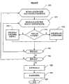
图3示出了并入了本发明的一些方面的示例性数字集成电路设计流程的简化表示。在高层级,该过程开始于产品构思(步骤300),并且在EDA(电子设计自动化)软件设计过程(步骤310)中实现。当设计定稿时,可以将该设计进行流片(tap-out)(步骤340)。在流片之后,出现制作工艺(步骤350)以及封装和组装工艺(步骤360),从而最后产生成品集成电路芯片(结果370)。Figure 3 shows a simplified representation of an exemplary digital integrated circuit design flow incorporating aspects of the present invention. At a high level, the process starts with product conception (step 300) and is implemented in the EDA (Electronic Design Automation) software design process (step 310). When the design is finalized, the design may be tap-out (step 340). After tape-out, a fabrication process (step 350) and a packaging and assembly process (step 360) occur to finally produce finished integrated circuit chips (result 370).
EDA软件设计过程(步骤310)实际上包括多个步骤312-330,在此为简便起见以线性方式示出。在实际的集成电路设计过程中,特定的设计可能需要经过步骤返回,直到通过某些测试为止。类似地,在任何实际设计过程中,这些步骤可以按照不同顺序和组合出现。因此。该描述仅是通过特定集成电路设计的上下文和一般说明而不是作为具体或者推荐的设计流程的方式提供。现在将提供EDA软件设计过程(步骤310)的组成步骤的简要描述。The EDA software design process (step 310) actually includes a number of steps 312-330, shown here in a linear fashion for simplicity. In the actual IC design process, a particular design may need to go back through steps until certain tests are passed. Similarly, in any practical design process, these steps may occur in different orders and combinations. therefore. This description is provided by way of context and general illustration of a particular integrated circuit design only and not by way of a specific or recommended design flow. A brief description of the constituent steps of the EDA software design process (step 310) will now be provided.
系统设计(步骤312):设计者描述他们想要实现的功能,他们也可以进行如果-怎么样(what-if)规划以细化功能、检验成本等。硬件-软件架构划分可以出现在这一阶段。可以在这一步骤使用的来自Synopsys公司的示例性EDA软件产品包括Model Architect、Saber、System Studio和Design Ware产品。System design (step 312): Designers describe the functions they want to achieve, and they can also do if-how (what-if) planning to refine functions, test costs, and so on. A hardware-software architectural partition can occur at this stage. Exemplary EDA software products from Synopsys that can be used at this step include Model Architect, Saber, System Studio, and Design Ware product.
逻辑设计和功能验证(步骤314):在这一阶段,编写用于系统中的模块的VHDL或者Verilog代码,并且检验该设计的功能准确度。具体而言,检验该设计以保证响应于特定输入激励产生正确的输出。可以在这一步骤使用的来自Synopsys公司的示例性EDA软件产品包括VCS、VERA、DesignWare
综合和测试设计(步骤316):此处,将VHDL/Verilog转译成网表。可以针对目标技术优化网表。此外,出现允许检验成品芯片的测试的设计和实施。可以在这一步骤使用的来自Synopsys公司的示例性EDA软件产品包括Design CompilerPhysical Complier、TestCompiler、Power Compiler、FPGA Compiler、TetraMAX和DesignWare
网表验证(步骤318):在这一步骤中,检验网表与时序约束的相符性和与VHDL/Verilog源码的对应性。可以在这一步骤使用的来自Synopsys公司的示例性EDA软件产品包括Formality、PrimeTime和VCS产品。Netlist Verification (Step 318 ): In this step, check the compliance of the netlist with the timing constraints and the correspondence with the VHDL/Verilog source code. Exemplary EDA software products from Synopsys, Inc. that can be used at this step include Formality, PrimeTime and VCS products.
设计规划(步骤320):这里,构造和分析用于芯片的整个平面图以便进行定时和顶层布线。可以在这一步骤使用的来自Synopsys公司的示例性EDA软件产品包括Astro产品和IC Compiler产品。Design Planning (step 320): Here, the entire floor plan for the chip is constructed and analyzed for timing and top-level routing. Exemplary EDA software products from Synopsys, Inc. that can be used at this step include Astro products and IC Compiler products.
物理实现(步骤322):在这一步骤出现布置(对电路元件的定位)和布线(对电路元件的连接)以及电路版图的其他方面。可以在这一步骤使用的来自Synopsys公司的示例性EDA软件产品包括Astro产品和IC Compiler产品。该步骤通常使用从Synopsys公司获得的诸如Liverty的软件产品来针对特定制造工艺预先设计的库单元进行布置。此处,本发明的某些方面可以在库单元的设计期间出现。Physical Implementation (step 322): Placement (positioning of circuit elements) and routing (connection of circuit elements) and other aspects of circuit layout occur at this step. Exemplary EDA software products from Synopsys, Inc. that can be used at this step include Astro products and IC Compiler products. This step is typically placed using a software product such as Liverty available from Synopsys, Inc. to place library cells predesigned for a particular manufacturing process. Here, certain aspects of the invention can arise during the design of library elements.
分析和提取(步骤324):在该步骤中,在晶体管级验证电路功能,这又允许如果-怎么样的细化。可以在这一步骤使用的来自Synopsys公司的示例性EDA软件产品包括AstroRail、PrimeRail、PrimeTime和Star-RC/XT产品。Analysis and Extraction (step 324): In this step, circuit functionality is verified at the transistor level, which in turn allows if-what refinement. Exemplary EDA software products from Synopsys, Inc. that can be used at this step include the AstroRail, PrimeRail, PrimeTime and Star-RC/XT products.
物理验证(步骤326):在这一步骤中,执行各种检验功能以确保制造、电气问题、光刻问题和电路的正确性。可以在这一步骤使用的来自Synopsys公司的示例性EDA软件产品包括Hercules产品。Physical Verification (Step 326): In this step, various verification functions are performed to ensure manufacturing, electrical issues, lithography issues, and correctness of the circuit. Exemplary EDA software products from Synopsys, Inc. that can be used at this step include Hercules products.
流片(步骤327):该步骤(在某些设计流程可以将该步骤延迟直到步骤330)为产生用于光刻用途的投影式掩膜提供“流片”数据,该光刻用途用以产生成品芯片。在这个步骤中可以使用的来自Synopsys公司的示例性EDA软件产品包括CATS(R)系列产品。Tape-out (step 327): This step (in some design flows this step may be delayed until step 330) provides "tape-out" data for generating projection masks for lithographic purposes used to generate finished chips. Exemplary EDA software products from Synopsys, Inc. that can be used in this step include the CATS(R) series of products.
解析度增强(步骤328):这一步骤涉及到对版图的几何操作以提高设计的可制造性。可以在这一步骤使用的来自Synopsys公司的示例性EDA软件产品包括Proteus、ProteusAF和PSMGen产品。本文中本发明的某些方面也可以在该步骤期间发生,或紧接该步骤发生。Resolution Enhancement (Step 328): This step involves geometric manipulation of the layout to improve the manufacturability of the design. Exemplary EDA software products from Synopsys, Inc. that can be used at this step include the Proteus, ProteusAF, and PSMGen products. Certain aspects of the invention herein may also occur during, or immediately after, this step.
投影式掩膜数据准备(步骤330):如果在解析度增强(步骤328)之前未执行,则这一步骤为产生用于光刻用途的投影式掩膜提供“流片”数据,该光刻用途用以产生成品芯片。Projected mask data preparation (step 330): If not performed prior to resolution enhancement (step 328), this step provides "tape-out" data for generating projected masks for lithographic use, which Uses are used to produce finished chips.
图4是图示了与本文讨论的一些实施例有关的设计流程的一些方面的流程图。与本文的所有流程图一样,将理解,在不影响所实现的功能的情况下,许多步骤可以组合执行、并行执行或者以不同的次序执行。在一些情况中,仅在也做出其他改变,步骤的重新布置才将会获得相同的结果,并且在其他一些情况中,只要满足某些条件,步骤的重新布置就将会获得相同的结果。Figure 4 is a flow diagram illustrating some aspects of the design flow in relation to some embodiments discussed herein. As with all flowcharts herein, it will be understood that many steps may be performed in combination, in parallel or in a different order without affecting the functionality implemented. In some cases, the rearrangement of steps will achieve the same result only if other changes are also made, and in other cases, as long as certain conditions are met, the rearrangement of steps will achieve the same result.
参照图4,在步骤410中设计电路。步骤410大体上对应于图3的步骤300和步骤312-步骤318。如此处所使用的,术语“电路设计”指代在从Verilog或者VHDL设计表示或者类似物编译之后,并且在布图之前的门级或者晶体管级设计。电路设计在步骤410之后表示在网表文件中。在步骤412中(大体上对应于图3的步骤320-步骤326),对电路设计进行布图。版图表示在几何文件中,该几何文件除其他以外,限定了将在待用于在制造期间使晶片曝光的每个投影式掩膜上形成的所有形状。几何文件可以具有若干标准格式中的任何格式,诸如GDSII、OASIS、CREF等,或者其可以具有非标准格式。该文件以针对将要生成的每个投影式掩膜的投影式掩膜定义的形式描述了电路设计的版图。每个投影式掩膜定义限定了多个多边形。在本实施例中的步骤412结束时,还未执行解析度增强(RET)。因此,从步骤412产生的版图几何在某种意义上是理想化的,这是由于它们还未考虑到使用与版图中的几何尺寸相当或者大于版图中的几何尺寸的光波长的光刻印刷的瑕疵。例如,矩形为直角的,并且还未针对衍射效应进行预校正。Referring to FIG. 4 , in
在步骤414中(大体上对应于步骤328),通过多个步骤来修订版图,以更好地实现设计者意图。从理想化的版图形状识别设计者的意图(诸如从沟道宽度识别的预期驱动电流),并且进行修改以更好地在最终集成电路中实现该意图。光学邻近校正在该步骤中出现,此后描述的形状设计凸块或者突起的添加也在该步骤中发生。通常使用以上几何文件格式之一来再次将经修订的版图表示在几何文件中。In step 414 (corresponding generally to step 328), the layout is revised through a number of steps to better achieve the designer's intent. The designer's intent (such as the expected drive current from the channel width) is identified from the idealized layout shape, and modifications are made to better realize that intent in the final integrated circuit. Optical proximity correction occurs in this step, as does the addition of shape-design bumps or protrusions described hereafter. The revised layout is represented again in a geometry file, typically using one of the above geometry file formats.
在步骤416中,基于来自步骤414的经修订的版图,创建光刻投影式掩膜组。用于形成投影式掩膜的方法并不是本发明的重要方面,所以可以使用任何投影式掩膜形成技术,不论是当今已知的还是将来开发的。作为一个示例,可以使用在美国专利No.6,096,458、No.6,057,063、No.5,246,800、No.5,472,814以及No.5,702,847中阐述的技术来印刷投影式掩膜,由于这些专利对投影式掩膜印刷金属的教导而将这些专利通过引用全部并入于此。In
在形成投影式掩膜组之后,在步骤418中,使用这些投影式掩膜来制造集成电路。此外,用于从投影式掩膜组制造集成电路的特定方法并不是本发明的重要方面,所以可以使用任何制造工艺,不论是当今已知的还是未来将开发的。优选地,使用如以上描述的用于对源极扩散和漏极扩散进行掺杂的自对准技术。After the set of projected masks are formed, in
图5是图4中用于对电路进行布图的步骤的流程图细节。图5是高度演进的过程的简化,该过程的大多数细节对于理解本发明不重要,并且因此在附图中未示出。参照图5,在步骤510中,为在输入网表中指定的各个电路器件选择库单元。库单元包括(除其他以外)该器件所需的版图几何,包括电流路径扩散区域和栅极堆叠的布置。例如,一个库单元可以包括图1A中的版图形状110、112、114和116,以及用于限定相反沟道类型的若干晶体管的版图形状。FIG. 5 is a flowchart detail of the steps in FIG. 4 for laying out the circuit. Figure 5 is a simplification of a highly evolved process, most of the details of which are not important to understanding the invention and are therefore not shown in the drawing. Referring to FIG. 5, in
在步骤512中,根据电路设计将库单元布置在版图中,并且限定布线以将库单元在互连层中互连。在该步骤中考虑了许多因素,这些因素中的大多数因素对于本发明的理解不重要。然而,根据本发明的一个方面,所考虑的因素之一是:如果晶体管的电流路径扩散中的一个比另一个宽,则优选的是较宽的一个被指派为晶体管的源极,而较窄的一个被指派为漏极。在布置和布线算法中考虑的其他一些因素可能推翻这一优选,但是至少在布图和布线优化努力中考虑并且包括了这一优选。一旦确定哪个电流路径扩散区域为源极并且哪个为漏极,则基于该选择,对将所选择的扩散连接到电路中的器件的其余扩散的互连层进行布图。替代地,如果版图形状为使得不同尺寸的两个或者多个晶体管共享电流路径扩散区域,并且互换源极和漏极以改善一个晶体管对另一个晶体管具有相反的影响,则在本发明的一个方面中,可以将扩散分裂为两个。然后可以单独优化每个扩散,尽管代价是芯片面积增加。In
布图步骤412是高度迭代的。因此,在步骤514中,针对所使用的芯片面积、时序、功耗和许多其他因素分析所布图的电路,并且在步骤516中,确定所布图的电路性能是否可接受。如果不可接受,则该过程返回到步骤512,以尝试电路器件的不同布置或者布线(包括从先前的迭代重新考虑源极/漏极选择和分裂扩散),或者如果必要则返回到步骤510以针对电路器件选择不同的库单元,或者如果必要,则该过程甚至可以返回到步骤410(图4)以便以一些方式修改电路的设计。在步骤516确定了电路性能可接受之后,布图步骤412完成(步骤518)。
图5中示出的步骤的一般序列也应用于对针对技术库的预先定义的单元的版图。对完全电路设计的布图和对库单元的布图之间的显著不同包括:完全电路设计的基本构建块为库单元,而库单元的基本构建块大多数为单独的晶体管。The general sequence of steps shown in Figure 5 also applies to the layout of the predefined cells for the technology library. Significant differences between layout for a full circuit design and layout for a library cell include that the basic building blocks of a full circuit design are library cells, whereas the basic building blocks of a library cell are mostly individual transistors.
图5A是用于对库单元进行布图的设计过程的流程图。再一次,图5A是高度演进的过程的简化,该过程的大多数细节对于本发明的理解不重要并且因此在附图中未示出。参照图5A,在步骤530中,为在输入网表中指定的各个电路器件选择基本特征。在很大程度上,基本特征为扩散区域、栅极导体和互连。在步骤532中,根据库单元电路设计,对基本特征进行布图并且在合适时对它们进行组合。与步骤512一样,虽然在该步骤中考虑了许多因素,但是本发明的一个方面是:考虑的因素之一是如果晶体管的电流路径扩散中的一个比另一个宽,则优选的是较宽的一个被指派为晶体管的源极,而较窄的一个被指派为漏极。一旦确定哪个电流路径扩散区域为源极并且哪个为漏极,则基于该选择对将所选择的扩散连接到库单元中的器件的其余扩散的互连层进行布图。替代地,如果版图形状为使得不同尺寸的两个或者更多晶体管共享电流路径扩散区域,并且互换源极和漏极以改善一个晶体管对另一个晶体管具有相反的影响,则在本发明的一个方面中,可以将扩散分裂为两个。然后可以单独优化每一个,尽管代价是芯片面积增加。5A is a flowchart of a design process for laying out library cells. Again, Figure 5A is a simplification of a highly evolved process, most of the details of which are not important to the understanding of the invention and are therefore not shown in the figure. Referring to FIG. 5A, in
在步骤534中,针对所使用的芯片面积、时序、功耗和许多其他因素来分析所布图的电路,并且在步骤536中,确定所布图的电路性能是否可接受。如果不可接受,则该过程返回到步骤532,以尝试特征的不同布置或者布线(包括从先前的迭代重新考虑源极/漏极选择和分裂扩散),或者如果必要则返回到步骤530以选择不同的基本特征,或者如果必要,则该过程甚至可以返回到以一些方式修改库单元的设计。在步骤536确定了电路性能可接受之后,库单元的布图完成(步骤538)。In
晶体管沟道的形状设计Shape Design of Transistor Channel
如上所述,如果晶体管的较大扩散被指派为源极扩散,则具有延伸进入到晶体管的沟道区域的圆化拐角的扩散区域可以改善晶体管的Ioff性能。电路版图可以通过有意地变宽晶体管的与栅极接近的源极区域而利用该观测。提供改善的不是圆化拐角本身,而是在源极侧变宽的非矩形沟道。圆化拐角是获得这种沟道形状的一种方式,虽然圆化仅是二阶效应。一阶效应是倾斜,即源极侧比漏极侧宽。As mentioned above, a diffusion region with rounded corners extending into the channel region of the transistor can improve the Ioff performance of the transistor if the larger diffusion of the transistor is assigned as the source diffusion. The circuit layout can take advantage of this observation by intentionally widening the source region of the transistor close to the gate. It is not the rounded corners themselves that provide the improvement, but the non-rectangular channel that widens on the source side. Rounding the corners is one way to achieve this channel shape, although rounding is only a second order effect. The first order effect is the slope, i.e. the source side is wider than the drain side.
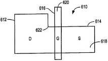
图6A是其中示出了一个晶体管610的电路版图的一部分的图示。晶体管610包括在栅极导体616的纵向相对侧上的第一电流路径扩散612和第二电流路径扩散614。扩散区域612被指派为漏极,并且扩散区域614被指派为源极,以及假定由于一些原因,电流路径端子的指派不可变。归因于在附图中未示出的原因,漏极扩散612比源极扩散614宽。例如,另一晶体管(未示出)可能位于扩散区域612内,电路设计要求该晶体管具有比所示出的晶体管大的驱动强度。在图6A中示出的是:扩散版图形状618,其为电流路径扩散612和电流路径扩散614与栅极导体616之下的沟道区域的几何联合;以及栅极多晶硅版图形状620。这些版图形状在步骤412之后表示在版图文件中。这些版图形状也表示为(如果在步骤414中未改变)将会用来制造集成电路的投影式掩膜组上的形状。为了讨论清楚起见,此处扩散形状618的拐角622被称为“内”拐角,这是由于当从形状618内部观察时其角度大于180度。如这里所使用的,“外”拐角是当从版图形状内部观察时角度小于180度的拐角。FIG. 6A is a diagram of a portion of a circuit layout in which one
如以上说明的,漏极扩散比源极扩散宽是有利的,这是由于延伸到栅极620之下的内部拐角622的任何圆化都将使性能尤其是Ioff退化。即使拐角622的圆化并不延伸到栅极620之下,Ioff性能仍然通过促使栅极之下的沟道扩散朝向源极扩散618变宽而得以改善。这可以以多种不同方式实现,并且图6B图示了实现以上的一种方式。As explained above, it is advantageous for the drain diffusion to be wider than the source diffusion, since any rounding of the
与图6A一样,图6B也是在版图文件和(如果在步骤414中未进行其他操作)在将要用来制造集成电路的投影式掩膜组上表示的扩散版图形状的图示。就在步骤414中执行了其他操作的程度而言,为了图示的清楚起见,图6B中的形状图示了在排除了这样的操作之后在投影式掩膜组上的形状。可以看出,已向扩散版图形状618添加了“凸块”或者“突起”624,该“凸块”或者“突起”624从扩散版图形状618的纵向边626横向地向外延伸,在所述栅极616的源极侧上纵向地延伸。突起624具有两个内拐角628和630,此处拐角628指代“邻近”栅极导体616的拐角,并且此处拐角630指代“远离”栅极导体616的拐角。此处突起624的横向定向的、与栅极导体邻近的边有时也称为“凹陷(jog)”。突起624的邻近拐角628布置成在版图上足够接近栅极616,从而使得在印刷到集成电路上期间,当拐角628由于光学衍射效应而圆化时,圆化拐角将至少部分地延伸到栅极616之下。可以针对这个拐角关闭光学邻近校正和/或其他解析度增强机制,以便避免干扰预期的圆化,或者如果光学邻近校正和/或其他解析度增强机制增强圆化拐角在栅极之下的圆化或者在其他方面以可特征化的方式修正圆化拐角,则可以允许针对该拐角进行光学邻近校正和/或其他解析度增强机制。Like FIG. 6A, FIG. 6B is an illustration of the diffusion layout shape represented on the layout file and (if no other operations were performed in step 414) on the projection mask set that will be used to fabricate the integrated circuit. To the extent that other operations were performed in
注意到,此处,在版图中的形状被视为彼此邻近或者远离,或者跨越彼此(如栅极620“跨越”扩散版图形状618),即使这些形状可能在不同的层上或者在投影式掩膜组的不同投影式掩膜上形成。这是在当层或者投影式掩膜叠加在彼此之上时平面图中的几何关系,其限定了此处所使用的“邻近”、“远离”或者“跨越”。附加地,此处叠置被视为仅是“邻近”的一个特殊情况,并且不与邻近进行区分。Note that here, shapes in the layout are considered to be adjacent to or far from each other, or straddle each other (eg,
图6C图示了在使用包含在图6B中所示的版图形状的投影式掩膜组形成的集成电路器件上的源极、漏极和沟道区域的形状。可以看出,内拐角628已经圆化,并且圆化部分地延伸到栅极导体616之下。更具体地,在源极扩散在位置L0处与沟道扩散相交时,在纵向位置的沟道宽度为W0。在沟道区域内存在另一纵向位置L1,在此处,沟道宽度为W1。由于拐角628的圆化,W1<W0。在图6B和图6C的实施例中,在纵向位置L2处(此处沟道区域与漏极扩散相交)的沟道宽度W2等于W1,这是由于拐角622的圆化并不延伸到栅极616之下。然而,在另一实施例中,W2可以比W1大。6C illustrates the shape of source, drain and channel regions on an integrated circuit device formed using a projected mask set containing the layout shape shown in FIG. 6B. It can be seen that the
如此处所使用的,无意对布置在衬底主体本身中或者布置在覆盖层中的集成电路的物品进行区分。例如,集成电路的所有特征(包括阱、扩散、STI区域、栅极电介质、栅极导体、金属层和盖层材料)均同等地描述为“在衬底上”或者“在衬底中”,并且无意在以上两个词中进行区分。附加地,如此处所使用的,术语“在…上面”和“在…下面”并不排除在其间存在一个或者多个材料或者层。As used herein, no distinction is intended to be made between items of integrated circuits arranged in the substrate body itself or in the cover layer. For example, all features of an integrated circuit, including wells, diffusions, STI regions, gate dielectrics, gate conductors, metal layers, and capping materials, are equally described as being "on" or "in" a substrate, And there is no intention to make a distinction between the above two words. Additionally, as used herein, the terms "on" and "under" do not preclude the presence of one or more materials or layers therebetween.
图7A是其中示出了一个晶体管710的电路版图的另一部分的图示。晶体管710包括在栅极导体716的纵向相对侧上的第一电流路径扩散712和第二电流路径扩散714。与在图6A中一样,扩散区域712被指派为漏极,并且扩散区域714被指派为源极,以及假定由于一些原因,电流路径端子的指派不可变。归因于在附图中未示出的原因,漏极扩散712比源极扩散714宽。在图7A中示出了扩散版图形状718,其为电流路径扩散712和电流路径扩散714与栅极导体716之下的沟道区域的几何联合;以及栅极多晶硅版图形状720。这些版图形状在步骤412之后表示在版图文件中。这些版图形状也表示为(排除在步骤414中的其他改变)将会用来制造集成电路的投影式掩膜组上的形状。FIG. 7A is a diagram of another portion of the circuit layout in which one
图7B也是在版图文件和(排除在步骤414中的任何其他操作)在将要用来制造集成电路的投影式掩膜组上表示的扩散版图形状的图示。图7B与图6B的不同之处在于,其图示了在扩散版图形状的两个横向相对纵向边上添加了突起,而不是如图6B仅在一个边上。因此,可以看出,已向扩散版图形状718添加了突起724A,该突起724A向外朝向扩散版图形状718的一个纵向边726A横向地延伸,其在栅极716的源极侧上纵向地延伸。已向扩散版图形状718添加了突起724B,该突起724B横向地从扩散版图形状718的另一个纵向边726B向外延伸,其纵向地在栅极716的源极侧上延伸。此处将两个突起724A和724B称为布置在扩散版图形状718的“横向相对”的纵向边726A和726B上。Figure 7B is also an illustration of the diffusion layout shape represented on the layout file and (excluding any other operations in step 414) on the projection mask set that will be used to fabricate the integrated circuit. FIG. 7B differs from FIG. 6B in that it illustrates the addition of protrusions on two laterally opposite longitudinal sides of the diffusion layout shape, rather than just one side as in FIG. 6B . Thus, it can be seen that a
突起724A的邻近内拐角为728A,并且突起724B的邻近内拐角为728B。这两者都布置在足够接近栅极716的版图上,从而使得在印刷到集成电路上期间,当拐角728A和拐角728B由于光学衍射效应而圆化时,圆化拐角将至少部分地延伸到栅极716之下。The adjacent inner corner of
图7C图示了在使用包含在图7B中所示的版图形状的投影式掩膜组形成的集成电路器件上的源极、漏极和沟道区域的形状。可以看出,内拐角728A和内拐角728B已经圆化,并且圆化部分地延伸到栅极导体716之下。更具体地,当源极扩散在纵向位置L0处与沟道扩散相交时,在纵向位置的沟道宽度为W0。在沟道区域内存在另一纵向位置L1,在此处,沟道宽度为W1。由于拐角728A和拐角728B的圆化,所以W1<W0。在沟道与源极扩散相交处,沟道已经在沟道横向相对的两个边上变宽。与在图6B和图6C的实施例中一样,在图7B和图7C的实施例中,在纵向位置L2处(此处沟道区域与漏极扩散相交)的沟道宽度W2等于W1,这是由于与在扩散版图形状718的漏极侧上的栅极导体716纵向地邻近的拐角722A和拐角722B的圆化并不延伸到栅极716之下。7C illustrates the shapes of source, drain and channel regions on an integrated circuit device formed using a projected mask set containing the layout shape shown in FIG. 7B. It can be seen that
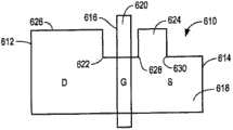
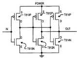
源极变宽的突起还可以被添加到如原始布图的不比源极宽的漏极处。图8A是2x缓冲器的电路版图的一部分的图示,其电路符号在图8D中示出。该2x缓冲器包括跨越P沟道扩散版图形状816和N沟道扩散版图形状818两者的三个栅极导体形状810、812和814,以在P沟道扩散版图形状816中形成相应的晶体管T810P、T812P和T814P,并且在N沟道扩散版图形状818中形成相应的晶体管T810N、T812N和T814N。因此,在P沟道扩散版图形状816中,栅极导体形状限定了电流路径扩散区域822、824、826和828。在N沟道扩散版图形状818中,栅极导体形状限定了电流路径扩散区域832、834、836和838。示出了用于将扩散822和扩散832连接到一起、将扩散826和扩散836连接到一起、将扩散824和828连接到电源总线以及将扩散834和838连接到接地总线的第一层金属互连的版图形状。示出了用于将信号输入端子连接到栅极导体810、将扩散822和扩散832连接到栅极导体812和栅极导体814这两者以及将信号输出端子连接到扩散826和扩散836的第二层金属互连的版图形状。由于这些互连,扩散区域822作为晶体管T810P的漏极连接,并且扩散区域824作为源极连接。这些互连在图8E中示出,而图8E是图8D的2x缓冲器的晶体管级电路图。A source widened protrusion can also be added where the drain is no wider than the source as in the original layout. Figure 8A is a diagram of a portion of the circuit layout of a 2x buffer, the circuit symbol of which is shown in Figure 8D. The 2x buffer includes three gate conductor shapes 810, 812 and 814 spanning both P-channel
如图8A中进一步示出的,源极区域824作为晶体管T812P的源极区域共享,并且扩散区域826是晶体管T812P的漏极。漏极区域826作为晶体管T814P的漏极区域共享,并且扩散区域828为T814P的漏极。类似地,扩散区域832作为晶体管T810N的漏极连接,并且扩散区域834作为源极连接。源极区域834作为晶体管T812N的源极区域共享,并且扩散区域836作为晶体管T812N的漏极。漏极区域836作为晶体管T814N的漏极共享,并且扩散区域838为晶体管T814N的漏极。与图6A和图7A中不同,扩散版图形状816的两个横向相对的纵向边840A和840B并不凹陷,而是在纵向上笔直地沿着扩散版图形状816的整个长度。类似地,扩散版图形状818的两个横向相对的纵向边842A和842B并不凹陷,而是在纵向上笔直地沿着扩散版图形状818的整个长度。如与针对图6A和图7A的一样,图8A中示出的在步骤412之后的版图形状表示在版图文件中。这些版图形状也表示为(如果在步骤414中未修改)在将要用来制造集成电路的投影式掩膜组上的形状。As further shown in FIG. 8A ,
图8B是表示在版图文件和(排除了在步骤414中执行的任何其他操作)在将要用来制造集成电路的投影式掩膜组上的扩散版图形状的图示。与在图7B中一样,在源极扩散区域824、828、834和838中的每个的扩散版图形状的横向相对的两个纵向边上添加了突起。因此,已在源极区域824的横向相对的边上添加了突起824A和突起824B;已在源极区域828的横向相对的边上添加了突起828A和突起828B;已在源极区域834的横向相对的边上添加了突起834A和突起834B;以及已在源极区域838的横向相对的边上添加了突起838A和突起838B。所有晶体管的漏极扩散和沟道宽度与它们的原始宽度比已经变窄,其中原始宽度示出为虚线844(P-扩散)和虚线846(N-扩散)。与由于所添加的突起导致的源极区域的变宽一起,这具有的效果是与在图8A中的原始版图保持相同的平均沟道宽度。平均沟道宽度的保持对于某些设计工具可能是期望的,但是对于其他可能不是期望的。突起824A和突起824B具有邻近栅极导体810的相应的内拐角848A和内拐角848B,并且还具有邻近栅极导体812的相应的内拐角850A和内拐角850B。突起828A和突起828B具有邻近栅极导体814的相应的内拐角852A和内拐角852B。类似地,突起834A和突起834B具有与栅极导体810邻近的相应的内拐角854A和内拐角854B,并且还具有与栅极导体812邻近的相应的内拐角856A和内拐角856B。突起838A和突起838B具有与栅极导体814邻近的相应的内拐角858A和858B。内拐角848A、848B、850A、850B、852A、852B、854A、854B、856A、856B、858A和858B中的所有这些均在版图上布置为足够接近它们邻近的相应栅极,从而使得在印刷到集成电路上期间,当这些拐角由于光学衍射效应而圆化时,圆化拐角将至少部分延伸到相应的栅极导体810、812和814之下。Figure 8B is a diagram representing the shape of the diffusion layout on the layout file and (excluding any other operations performed in step 414) on the projection mask set that will be used to fabricate the integrated circuit. As in FIG. 7B , protrusions are added on two laterally opposite longitudinal sides of the diffusion layout shape of each of the
图8C图示了在使用包含如在图8B中所示的版图形状的投影式掩膜组形成的集成电路器件上的源极、漏极和沟道扩散、以及多晶硅栅极和金属互连的形状。可以看出,所有内拐角已经圆化,并且圆化部分地延伸到它们相应的邻近栅极导体810、812或者814之下。更具体地(并且关于晶体管T812N作为一个示例所示出地),当源极扩散834在纵向位置L0处与沟道扩散相交时,在纵向位置的沟道宽度为W0。在沟道区域内在纵向上存在另一纵向位置L1,在此处,沟道宽度为W1。由于拐角856A和拐角856B的圆化,所以W1<W0。在沟道与源极扩散相交处沟道已经有效地变宽,并且在沟道与漏极区域相交处处沟道已经有效地变窄。8C illustrates source, drain, and channel diffusions, as well as polysilicon gate and metal interconnects, on an integrated circuit device formed using a projected mask set containing the layout shape as shown in FIG. 8B. shape. It can be seen that all inner corners have been rounded and that the rounding extends partially below their respective
除了横向地延伸源极扩散区域的突起之外,在一些情况中,可能有理由同样地横向地延伸漏极扩散区域。例如,对于具有SiGe扩散区域的P沟道晶体管而言,较宽的电流路径扩散可以增加附近的有益应力,从而增强载流子迁移率。这对于具有Si:C扩散区域的N沟道晶体管也是如此。无论是将突起添加到源极扩散还是漏极扩散,都能观测到这种改善,并且事实上,如果添加到两个扩散则这种改善最显著。In addition to extending the protrusions of the source diffusion region laterally, in some cases it may be reasonable to also extend the drain diffusion region laterally. For example, for P-channel transistors with SiGe diffused regions, wider current path diffusions can increase the beneficial stress in the vicinity, thereby enhancing carrier mobility. This is also true for N-channel transistors with Si:C diffused regions. This improvement is observed regardless of whether the protrusion is added to the source or drain diffusion and, in fact, is most pronounced if added to both diffusions.
图9A、图9B和图9C图示了利用该观测的晶体管版图。再一次,图9A图示了在版图文件中表示的在步骤412之后的原始版图形状。这些版图形状(排除在步骤414中的任何其他修改)也表示在将要用来制造集成电路的投影式掩膜组上的形状。示出了源极区域和漏极区域,以及用于限定沟道的栅极版图形状。图9B图示了在将横向延伸的突起添加到扩散版图形状的两个横向边并且在源极区域和漏极区域两者中之后的版图形状。再一次,与栅极版图形状邻近的突起的内拐角被布置成足够接近栅极版图形状(或者在栅极版图形状之下),从而使得在印刷到集成电路期间,当邻近拐角由于光学衍射效应而圆化时,这些圆化拐角将至少部分地延伸到栅极导体之下。注意到,利用横向切入的切口(cut-out)而不是两个横向延伸的突起也能实现相同的效果。9A, 9B and 9C illustrate transistor layouts utilizing this observation. Again, Figure 9A illustrates the original layout shape after
图9C图示了在使用包含如在图9B中所示的版图形状的投影式掩膜组形成的集成电路器件上的源极、漏极和沟道扩散的形状。可以看出,所有四个邻近内拐角已经圆化,并且圆化部分地延伸到栅极导体之下。更具体地,当源极扩散在纵向位置L0处与沟道扩散相交时,在纵向位置的沟道宽度为W0。在沟道区域内、纵向上存在另一纵向位置L1,在此处,沟道宽度为W1,并且当漏极扩散在纵向位置L2处与沟道扩散相交时,沟道宽度为W2。由于四个邻近内拐角的圆化,所以W1<W0以及W1<W2。在图9C的实施例中,进一步对于W2=W0也成立,但是这在本发明的所有实施例中并不重要。Figure 9C illustrates the shape of source, drain and channel diffusions on an integrated circuit device formed using a projected mask set containing the layout shape as shown in Figure 9B. It can be seen that all four adjacent inner corners have been rounded, and that the rounding extends partially below the gate conductor. More specifically, when the source diffusion intersects the channel diffusion at the longitudinal position L0, the channel width at the longitudinal position is W0. Within the channel region, longitudinally there is another longitudinal position L1 where the channel width is W1 and when the drain diffusion intersects the channel diffusion at longitudinal position L2 the channel width is W2. Due to the rounding of the four adjacent inner corners, W1<W0 and W1<W2. In the embodiment of FIG. 9C it is further true for W2=W0, but this is not important in all embodiments of the invention.
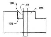
在以上描述的大多数实施例中,已经引入的横向延伸的凹陷纵向地布置在栅极版图形状的源极侧上。作为凹陷的结果,与栅极版图形状邻近的内拐角在光刻投射到器件上期间圆化,并且从而部分延伸进入到沟道区域中。图10A图示了可以基于图6A的原始版图获得非矩形沟道的另一方式。在图10A中,与突起624(图6)类似地添加了突起1010,但是凹陷1012纵向地布置在栅极版图形状的漏极侧。作为凹陷的结果,凹陷的外拐角1014在光刻投射到器件期间圆化,并且从而部分延伸进入到沟道区域中。这在图10B中示出。注意到,类似于凹陷1012的凹陷可以被视为由于所添加的突起1010或者由于横向切入的切口1016所导致的;以上任何一种描述都是精确的。In most of the embodiments described above, the laterally extending recesses that have been introduced are arranged longitudinally on the source side of the gate layout shape. As a result of the dishing, inner corners adjacent to the gate layout shape are rounded during lithographic projection onto the device, and thus partly extend into the channel region. Figure 1OA illustrates another way in which non-rectangular channels can be obtained based on the original layout of Figure 6A. In FIG. 10A , a
图11A图示了可以基于图6A的原始版图获得非矩形沟道的另一方式。在图11A中,与突起624(图6)类似地添加了突起1110,但是凹陷1112纵向地布置在源极区域和漏极区域之间,在将要由栅极版图形状限定的沟道内。作为该凹陷的结果,凹陷的内拐角1114和外拐角1116将至少部分地位于沟道区域内,即使在两个拐角的衍射圆化之后也是如此。这在图11B中示出。FIG. 11A illustrates another way in which non-rectangular channels can be obtained based on the original layout of FIG. 6A. In FIG. 11A , a
图12A图示了可以用来获得非矩形沟道的其他两种变形:可以在漏极侧使用横向切入的切口而不是在源极侧上的突起,以及可以以台阶方式使用两个或者多于两个凹陷。可独立使用任一变形,或者它们可以如在图12A中示出的一起使用。在图12A中,与突起624(图6)类似地添加了突起1210,而凹陷1212纵向地布置在源极扩散区域中。凹陷1212具有与栅极版图形状邻近的内拐角1214,其被布置成在纵向上足够接近栅极版图形状,从而使得当内拐角1214在光刻曝光期间由于衍射效应而圆化时,内拐角1214将部分地延伸进入沟道区域。这可以在图12B中看出。此外,已在扩散版图形状中形成切口1216,而邻近凹陷1218纵向地布置在漏极扩散区域中。凹陷1218具有与在横向方向上与拐角1214邻近的外拐角1220,并且该外拐角被布置成在纵向上足够接近栅极版图形状,从而使得当外拐角1220在光刻曝光期间由于衍射效应而圆化时,该外拐角1220将部分地延伸进入沟道区域。这也可以在图12B中看出。Figure 12A illustrates two other variations that can be used to obtain a non-rectangular channel: a laterally-cut incision can be used on the drain side instead of a protrusion on the source side, and two or more than two can be used in a stepped manner. Two depressions. Either variant can be used independently, or they can be used together as shown in Figure 12A. In FIG. 12A , a
将理解,在图10A、图11A和图12A中所图示的所有变形同样适用于图7B、图8B和图9B。也存在许多其他变形,包括诸如在图12A中示出的其中凹陷1212和凹陷1218中的一个或者两个在栅极版图形状之下纵向地出现,以及包括三个或者更多凹陷的变形。其他变形包括其中凹陷还在扩散版图形状的相对纵向边上出现的那些变形。此外,如果版图软件和投影式掩膜制作工艺允许,则凹陷也可以对角线地形成,而不是直线地形成。It will be understood that all variations illustrated in Figures 10A, 11A and 12A apply equally to Figures 7B, 8B and 9B. There are also many other variations, including such as shown in FIG. 12A where one or both of the
用于在沟道中引入非矩形的设计流程Design Flow for Introducing Non-Rectangular Channels
回到图4,将非矩形引入到晶体管沟道中的步骤(诸如在图6C、图7C和图8C中示出的)可以在步骤414(即,操纵版图以更好地实现设计者意图)期间执行。图13是步骤414的流程图细节,具体地是用于对版图进行修订以改善Ioff电流。图13的步骤可以作为步骤512(图5)或者步骤532(图5A)的一部分执行。读者将会清楚如何修改附图13,以同样由于以上关于图9B描述的应力效应而改善载流子迁移率。参照图13,在步骤1310中,系统开始经过所有扩散版图形状(针对引入延伸到晶体管栅极导体之下的圆化拐角)的循环。这些形状可以是在整个版图的特定部分中的所有扩散版图形状,或者可以通过一些其他特性而选择这些形状。在步骤1312中,内部循环开始经过被指定为源极扩散的、当前扩散版图形状中的所有扩散子区域。在步骤1314中,确定当前源极扩散是否已经比沟道宽。如果是,则不需要附加的突起。相反,在步骤1316中,不过度地冒着稍微未对准的步进机将把凹陷本身印刷成与栅极导体叠置的风险的情况下,将在源极区域中的扩散版图形状中的并且邻近栅极导体的凹陷移动到尽可能接近栅极导体的纵向位置(如果还未在该处)。旨在使得凹陷的邻近内拐角在印刷到集成电路上期间圆化之后部分地延伸到栅极导体之下。Returning to FIG. 4, the step of introducing non-rectangularity into the transistor channel (such as shown in FIGS. 6C, 7C, and 8C) can be performed during step 414 (i.e., manipulating the layout to better achieve the designer's intent). implement. FIG. 13 is a flowchart detail of
另一方面,如果源极与沟道一样宽或者比沟道窄,则在步骤1316中,诸如在图6B、图7B和图8B中示出的突起被纵向地添加到在纵向上在栅极导体与源极区域一样的相同侧上的扩散版图形状上。再一次,选择足够接近栅极导体的纵向位置,从而使得突起的邻近内拐角在印刷到集成电路上期间圆化之后至少部分地延伸到栅极导体之下,但是不会太接近以过度地冒着稍微未对准的步进机将把突起本身印刷成与栅极导体叠置的风险。将理解,在一个实施例中,突起可以在横向方向上添加到源极区域的一个边上,而在不同的实施例中,突起可以在横向方向上添加到源极区域的两个相对边上。On the other hand, if the source is as wide as or narrower than the channel, then in step 1316 a protrusion such as that shown in Figures 6B, 7B and 8B is added longitudinally to the gate The conductor is on the diffusion pattern shape on the same side as the source region. Again, the longitudinal position of the gate conductor is chosen close enough so that the adjacent inner corners of the protrusion at least partially extend below the gate conductor after being rounded during printing onto the integrated circuit, but not so close as to unduly risk There is a risk that a slightly misaligned stepper will print the bump itself overlapping the gate conductor. It will be appreciated that in one embodiment, protrusions may be added in a lateral direction to one side of the source region, while in a different embodiment, protrusions may be added in a lateral direction on two opposite sides of the source region. .
在步骤1316中的源极区域凹陷的任何移动之后,或者在步骤1318中添加了任何突起之后,在步骤1320中确定在当前扩散版图形状中是否存在更多的源极区域。如果存在,则系统回到步骤1312以考虑当前版图形状中的下一源极区域。如果不存在,则在步骤1322中,系统确定是否存在需要考虑的更多扩散版图形状。如果存在,则系统返回到步骤1310以考虑下一扩散版图形状。After any movement of source region recesses in
在已经考虑了所有期望的扩散版图形状之后,可以在步骤1324中添加对版图中各种形状的光学邻近校正。如以上提到的,可以针对在步骤1316或者1318中受到影响的或者考虑的拐角关闭光学邻近校正和/或其他解析度增强机制,以便避免干扰预期的圆化,或者如果光学邻近校正和/或其他解析度增强机制增强拐角在栅极之下的圆化程度或者在其他方面以可特征化的方式修正拐角,则可以允许针对这些拐角进行光学邻近校正和/或其他解析度增强机制。最后,在步骤1326中,可以对版图执行任何其他解析度增强或者其他操纵。注意到,步骤1326可以部分或者全部在步骤1324或者甚至1310之前执行,或者甚至在循环1310和循环1312的一个或者两个内执行,只要这些循环不会修改预期的圆化,或者确实修改圆化但是其是以可特征化的方式进行修改。优选地,光学邻近校正步骤1324仅在步骤1322之后出现,但是通过适当考虑,在特定实施例中其也可以早些执行。操纵版图的步骤在步骤1328中完成。After all desired diffusion layout shapes have been considered, optical proximity corrections for the various shapes in the layout may be added in
图14是可以用来实现并入本发明的一些方面的软件的计算机系统1410的简化方框图。计算机系统1410包括经由总线子系统1412与许多外围设备通信的处理器子系统1414。这些外围设备可以包括存储子系统1424(包括存储器子系统1426以及文件存储子系统1428),用户接口输入设备1422、用户接口输出设备1420以及网络接口子系统1416。输入和输出设备允许用户与计算机系统1410交互。网络接口子系统1416提供到外部网络的接口(包括到通信网络1418的接口)并且经由通信网络1418耦合到其它计算机系统中的相应接口设备。通信网络1418可以包括多个互连的计算机系统和通信链路。这些通信链路可以是有线链路、光学链路、无线链路或者用于信息通信的任何其它机制。尽管在一个实施例中,通信网络1418是因特网,但是在其它实施例中,通信网络1418可以是任何适合的计算机网络。Figure 14 is a simplified block diagram of a
网络接口的物理硬件部件有时称为网络接口卡(NIC),虽然它们不需要为卡的形式:例如,它们可以为直接适配到母板上的集成电路(IC)和连接器的形式,或者为与计算系统的其他部件一起的在单个集成电路芯片上制造的宏单元形式。The physical hardware components of the network interface are sometimes referred to as network interface cards (NICs), although they need not be in the form of cards: for example, they could be in the form of integrated circuits (ICs) and connectors that fit directly onto the motherboard, or A form of macrocell fabricated on a single integrated circuit chip with other components of a computing system.
用户接口输入设备1422可以包括键盘、定点设备(诸如鼠标、轨迹球、触摸板或者图形输入板)、扫描仪,并入到显示器内的触摸屏、音频输入设备(诸如语音识别系统、麦克风)及其它类型的输入设备。总之,术语“输入设备”的使用旨在包括用于将信息输入到计算机系统1410中或者到计算机网络1418上的所有可能类型的设备和方式。User
用户接口输出设备1420可以包括显示子系统、打印机、传真机或者诸如音频输出设备之类的非可视显示器。显示子系统可以包括阴极射线管(CRT)、诸如液晶显示器(LCD)的平板设备、投影设备或者一些用于创建可视图像的其它机制。显示子系统还可以诸如通过音频输出设备提供非可视显示。一般而言,术语“输出设备”的使用旨在包括用于从计算机系统1410向用户或者其它机器或计算机系统输出信息的所有可能类型的设备和方式。User
存储子系统1424存储提供本发明的某些实施例的功能的基本编程和数据结构。例如,实现发明某些实施例的功能的各种模块可以存储在存储子系统1424中。这些软件模块通常由处理器1414执行。
存储器子系统1426典型地包括多个存储器,这些存储器包括用于在程序执行期间存储指令和数据的主随机访问存储器(RAM)1430和在其中存储固定指令的只读存储器(ROM)1432。文件存储子系统1428为程序和数据文件提供持久存储,其并且可以包括硬盘驱动器、与可移除介质相关的软盘驱动器、CD-ROM驱动器、光盘驱动器或者其它可移除介质盒式磁带。实现本发明某些实施例的功能的数据库和模块可由文件存储子系统1428存储。主机存储器1426包含(除其他以外)当由处理器子系统1414执行时促使计算机系统操作或者执行本文描述的功能的计算机指令。如这里所使用的,称为在“主机”或者“计算机”中或者“主机”或者“计算机”上运行的过程和软件响应于主机存储器子系统1426(包括用于存储这种指令和数据的任何其他本地或者远程存储)中的计算机指令和数据而在处理器子系统1414上执行。
总线子系统1412提供用于使计算机系统1410的各种组件和子系统如所期望地彼此通信的机制。尽管总线子系统1412被示意性地示出为单个总线,但是总线子系统的备选实施例可以使用多个总线。
计算机系统1410本身可以是各种类型的,其包括个人计算机、便携式计算机、工作站、计算机终端、网络计算机、电视、大型机或者任何其它数据处理系统或用户设备。由于计算机和网络经常改变的性质,图14中描绘的计算机系统1410的描述仅意味着作为为了图示本发明某些实施例的特定例子。计算机系统1410的许多其它配置可能与图14中描述的计算机系统相比具有更多或更少的部件。
在图5和图13中阐述的步骤通过具有处理器(诸如处理器子系统1414)和存储器(诸如存储子系统1424)的计算机系统,在包括指令的软件的控制下执行,这些指令可由处理器子系统1414执行,从而执行所示出的步骤。该软件还包括处理器对其操作的数据。该软件存储在计算机可读存储介质上,如在此所使用的,该计算机可读介质是在其上存储信息并且这些信息可以由计算机系统读取的介质。示例包括但不限于软盘、硬盘驱动、RAM、CD、DVD、闪存、USB驱动等。计算机可读介质可以存储以编码格式的信息,在特定数据处理系统中对这些编码格式进行解码以供实际使用。如这里所使用的,单个计算机可读介质也可以包括多于一个的物理项,诸如多个CD-ROM或者RAM的多个段或者若干不同种介质的组合。当存储软件的计算机可读介质与图14的计算机系统组合时,该组合为执行本文阐述的步骤的机器。用于执行每个步骤的装置包括计算机系统(或者仅执行该步骤所需的计算机系统的部分)与用于执行该步骤的软件模块的组合。存储软件的计算机可读介质也能够与计算机系统单独分布,并且形成其自身的制品。The steps set forth in FIGS. 5 and 13 are performed by a computer system having a processor, such as
另外,在步骤412和步骤414两者之后,网表文件或者包含电路设计的表示的文件,以及几何文件或者存储版图的文件这些它们本身存储在计算机可读介质上。这样的介质可以与计算机系统单独分布,并且形成它们自身相应的制品。当与使用软件编程的计算机系统相结合以供对网表或者几何文件进行读取、修订和写入时,它们形成执行这里阐述的步骤的又一机器。Additionally, following both
出于示例和描述的目的已经提供了对本发明实施例的前文描述。本意并非让它们穷举本发明或者使本发明限于所公开的形式。很明显,本领域技术人员将清楚许多修改和变化。例如,虽然一种用于形成延伸到栅极之下的圆化拐角的方法涉及在图6B、7B、8B和9B所示的版图形状添加突起,但是将理解,也可以使用其他方法。具体地,例如,可以使用反向光刻技术作为替代。反向光刻在以下文章中描述:可从http://www.solid-state.com/display_article/311162/28/ARTCL/none/none/1/Double-exposure-inverse-lithography获得的Milanfar、Borodovsky和Poonawala的″Double exposure inverselithography″(11/2007),以及可从http://www.semiconductor.net/article/CA6434690.html获得的AaronHand的″Inverse Lithography Makes New Inroads in RET″(5/1/2007),这两篇文章都通过引用并入于此。此外,向版图形状添加的突起不必为如图6B、图7B、图8B以及图9B中所示的矩形。此外,在不限制的情况下,所描述的、暗示的或者通过引用并入到本专利申请背景技术部分中的任意和所有变形都通过引用具体地并入于此,以帮助表达本发明的实施例可以借此实现的技术的广度。本文所描述的实施例是为了最好地说明本发明的原理及其实际应用,从而使得本领域其他技术人员能够针对各种实施例和具有适于所考虑的特定应用的修改而理解本发明。本意是本发明的范围由下文权利要求及它们的等价物限定。The foregoing description of the embodiments of the invention has been presented for purposes of illustration and description. They are not intended to be exhaustive or to limit the invention to the form disclosed. Obviously, many modifications and changes will be apparent to those skilled in the art. For example, while one method for forming rounded corners that extend below the gate involves adding protrusions to the layout shapes shown in Figures 6B, 7B, 8B, and 9B, it will be appreciated that other methods may also be used. Specifically, for example, reverse photolithography may be used instead. Inverse lithography is described in the following article: Milanfar, Borodovsky and Poonawala's "Double exposure inverselithography" (11/2007), and Aaron Hand's "Inverse Lithography Makes New Inroads in RET" (5/1/ 2007), both of which are incorporated herein by reference. Furthermore, the protrusions added to the layout shape do not have to be rectangular as shown in Figures 6B, 7B, 8B and 9B. Furthermore, without limitation, any and all variations that are described, implied, or incorporated by reference in the Background section of this patent application are hereby specifically incorporated by reference to aid in expressing the practice of this invention examples of the breadth of techniques that can be achieved through this. The embodiments described herein are in order to best explain the principles of the invention and its practical application, to thereby enable others skilled in the art to understand the invention for various embodiments and with modification as are suited to the particular application contemplated. It is intended that the scope of the invention be defined by the following claims and their equivalents.
Claims (21)
Translated fromChineseApplications Claiming Priority (5)
| Application Number | Priority Date | Filing Date | Title |
|---|---|---|---|
| US20608309P | 2009-01-27 | 2009-01-27 | |
| US61/206,083 | 2009-01-27 | ||
| US12/390,338US20100187609A1 (en) | 2009-01-27 | 2009-02-20 | Boosting transistor performance with non-rectangular channels |
| US12/390,338 | 2009-02-20 | ||
| PCT/US2009/062635WO2010087884A1 (en) | 2009-01-27 | 2009-10-29 | Boosting transistor performance with non-rectangular channels |
Publications (1)
| Publication Number | Publication Date |
|---|---|
| CN102365740Atrue CN102365740A (en) | 2012-02-29 |
Family
ID=42353479
Family Applications (1)
| Application Number | Title | Priority Date | Filing Date |
|---|---|---|---|
| CN2009801583669APendingCN102365740A (en) | 2009-01-27 | 2009-10-29 | Using non-rectangular channels to boost transistor performance |
Country Status (4)
| Country | Link |
|---|---|
| US (3) | US20100187609A1 (en) |
| CN (1) | CN102365740A (en) |
| TW (1) | TW201114013A (en) |
| WO (1) | WO2010087884A1 (en) |
Cited By (5)
| Publication number | Priority date | Publication date | Assignee | Title |
|---|---|---|---|---|
| CN103165575A (en)* | 2011-12-13 | 2013-06-19 | 格罗方德半导体公司 | Semiconductor device with transistor local interconnects |
| CN104471714A (en)* | 2012-06-13 | 2015-03-25 | 美商新思科技有限公司 | N-channel and P-channel end-to-end FinFET cell architecture |
| CN104916634A (en)* | 2014-03-11 | 2015-09-16 | 三星电子株式会社 | Methods of preparing layouts for semiconductor devices, photomasks formed using the layouts, and semiconductor devices fabricated using the photomasks |
| CN106098563A (en)* | 2016-08-25 | 2016-11-09 | 武汉华星光电技术有限公司 | Narrow frame display floater, thin film transistor (TFT) and preparation method thereof |
| WO2024021178A1 (en)* | 2022-07-29 | 2024-02-01 | 广州华星光电半导体显示技术有限公司 | Array substrate and display panel |
Families Citing this family (19)
| Publication number | Priority date | Publication date | Assignee | Title |
|---|---|---|---|---|
| US7446352B2 (en) | 2006-03-09 | 2008-11-04 | Tela Innovations, Inc. | Dynamic array architecture |
| US7763534B2 (en) | 2007-10-26 | 2010-07-27 | Tela Innovations, Inc. | Methods, structures and designs for self-aligning local interconnects used in integrated circuits |
| US8541879B2 (en) | 2007-12-13 | 2013-09-24 | Tela Innovations, Inc. | Super-self-aligned contacts and method for making the same |
| US9563733B2 (en)* | 2009-05-06 | 2017-02-07 | Tela Innovations, Inc. | Cell circuit and layout with linear finfet structures |
| US7956421B2 (en) | 2008-03-13 | 2011-06-07 | Tela Innovations, Inc. | Cross-coupled transistor layouts in restricted gate level layout architecture |
| US8151221B2 (en)* | 2010-04-29 | 2012-04-03 | United Microelectronics Corp. | Method to compensate optical proximity correction |
| US9355209B2 (en)* | 2011-11-17 | 2016-05-31 | Taiwan Semiconductor Manufacturing Company, Ltd. | Revising layout design through OPC to reduce corner rounding effect |
| US8703595B2 (en) | 2011-11-17 | 2014-04-22 | Taiwan Semiconductor Manufacturing Company, Ltd. | N/P boundary effect reduction for metal gate transistors |
| US8776005B1 (en) | 2013-01-18 | 2014-07-08 | Synopsys, Inc. | Modeling mechanical behavior with layout-dependent material properties |
| US9318607B2 (en)* | 2013-07-12 | 2016-04-19 | Samsung Electronics Co., Ltd. | Semiconductor device and method of fabricating the same |
| US9158878B2 (en)* | 2013-08-23 | 2015-10-13 | Kabushiki Kaisha Toshiba | Method and apparatus for generating circuit layout using design model and specification |
| US9564375B2 (en)* | 2013-10-15 | 2017-02-07 | Globalfoundries Inc. | Structures and methods for extraction of device channel width |
| KR20150087725A (en)* | 2014-01-22 | 2015-07-30 | 삼성전자주식회사 | Method of simulating a semiconductor device and method of designing a semiconductor memory device using the same |
| US9337099B1 (en)* | 2015-01-30 | 2016-05-10 | Globalfoundries Inc. | Special constructs for continuous non-uniform active region FinFET standard cells |
| JP5905630B1 (en)* | 2015-08-13 | 2016-04-20 | 株式会社フローディア | Manufacturing method of semiconductor integrated circuit device and semiconductor integrated circuit device |
| KR102661932B1 (en)* | 2016-12-16 | 2024-04-29 | 삼성전자주식회사 | Integrated circuit for multiple patterning lithography, computing system and computer-implemented method for designing integrated circuit |
| JP7321049B2 (en)* | 2019-10-11 | 2023-08-04 | キヤノン株式会社 | Light-emitting devices, display devices, photoelectric conversion devices, electronic devices, lighting devices, and moving bodies |
| KR20220128040A (en)* | 2021-03-12 | 2022-09-20 | 삼성전자주식회사 | semiconductor device |
| US20230095459A1 (en)* | 2021-09-28 | 2023-03-30 | Arm Limited | Logic Cell Structure with Diffusion Box |
Citations (10)
| Publication number | Priority date | Publication date | Assignee | Title |
|---|---|---|---|---|
| DE4037492A1 (en)* | 1990-11-26 | 1992-05-27 | Ernst Prof Dr Ing Lueder | FET with semiconductor in channel between drain and source electrode - whose length for drain-source current has irregular cross=section between both electrodes |
| JPH08172136A (en)* | 1994-09-30 | 1996-07-02 | Sharp Corp | Method of forming MOS inverter |
| US20020083408A1 (en)* | 2000-09-07 | 2002-06-27 | Henning Haffner | Generating mask layout data for simulation of lithographic processes |
| US20050180219A1 (en)* | 2003-12-05 | 2005-08-18 | Ryuji Ohba | Random number generating element |
| US7137089B1 (en)* | 2004-09-01 | 2006-11-14 | National Semiconductor Corporation | Systems and methods for reducing IR-drop noise |
| US20070096158A1 (en)* | 2005-10-31 | 2007-05-03 | Fujitsu Limited | Pattern layout and layout data generation method |
| US20070128777A1 (en)* | 2005-12-02 | 2007-06-07 | Samsung Electronics Co., Ltd | POLY-Si THIN FILM TRANSISTOR AND ORGANIC LIGHT-EMITTING DISPLAY HAVING THE SAME |
| US20080107974A1 (en)* | 2006-09-27 | 2008-05-08 | Toshiaki Douzaka | Photomask, multiphase exposure method, and method of manufacturing semiconductor device including insulating gate-type transistors |
| US20080185666A1 (en)* | 2007-02-05 | 2008-08-07 | Samsung Electronics Co., Ltd. | Field effect transistors including variable width channels and methods of forming the same |
| US20080197394A1 (en)* | 2007-02-20 | 2008-08-21 | Qimonda Ag | Methods of manufacturing semiconductor structures |
Family Cites Families (8)
| Publication number | Priority date | Publication date | Assignee | Title |
|---|---|---|---|---|
| US5246800A (en)* | 1991-09-12 | 1993-09-21 | Etec Systems, Inc. | Discrete phase shift mask writing |
| KR100298610B1 (en)* | 1992-09-01 | 2001-11-30 | 기타지마 요시토시 | Phase Shift Photomask, Phase Shift Photomask Blank and Manufacturing Method thereof |
| US5472814A (en)* | 1994-11-17 | 1995-12-05 | International Business Machines Corporation | Orthogonally separated phase shifted and unphase shifted mask patterns for image improvement |
| US6057063A (en)* | 1997-04-14 | 2000-05-02 | International Business Machines Corporation | Phase shifted mask design system, phase shifted mask and VLSI circuit devices manufactured therewith |
| US6096458A (en)* | 1998-08-05 | 2000-08-01 | International Business Machines Corporation | Methods for manufacturing photolithography masks utilizing interfering beams of radiation |
| US6365947B1 (en)* | 2000-04-27 | 2002-04-02 | White Oak Semiconductor Partnership | Semiconductor device and method of increasing channel length to eliminate short channel effects of corner devices |
| US8296691B2 (en)* | 2008-01-08 | 2012-10-23 | International Business Machines Corporation | Methodology for improving device performance prediction from effects of active area corner rounding |
| US8001494B2 (en)* | 2008-10-13 | 2011-08-16 | Taiwan Semiconductor Manufacturing Company, Ltd. | Table-based DFM for accurate post-layout analysis |
- 2009
- 2009-02-20USUS12/390,338patent/US20100187609A1/ennot_activeAbandoned
- 2009-10-29WOPCT/US2009/062635patent/WO2010087884A1/enactiveApplication Filing
- 2009-10-29CNCN2009801583669Apatent/CN102365740A/enactivePending
- 2010
- 2010-01-12TWTW099100690Apatent/TW201114013A/enunknown
- 2011
- 2011-09-20USUS13/237,818patent/US8701054B2/enactiveActive
- 2014
- 2014-04-09USUS14/249,129patent/US8869078B2/enactiveActive
Patent Citations (10)
| Publication number | Priority date | Publication date | Assignee | Title |
|---|---|---|---|---|
| DE4037492A1 (en)* | 1990-11-26 | 1992-05-27 | Ernst Prof Dr Ing Lueder | FET with semiconductor in channel between drain and source electrode - whose length for drain-source current has irregular cross=section between both electrodes |
| JPH08172136A (en)* | 1994-09-30 | 1996-07-02 | Sharp Corp | Method of forming MOS inverter |
| US20020083408A1 (en)* | 2000-09-07 | 2002-06-27 | Henning Haffner | Generating mask layout data for simulation of lithographic processes |
| US20050180219A1 (en)* | 2003-12-05 | 2005-08-18 | Ryuji Ohba | Random number generating element |
| US7137089B1 (en)* | 2004-09-01 | 2006-11-14 | National Semiconductor Corporation | Systems and methods for reducing IR-drop noise |
| US20070096158A1 (en)* | 2005-10-31 | 2007-05-03 | Fujitsu Limited | Pattern layout and layout data generation method |
| US20070128777A1 (en)* | 2005-12-02 | 2007-06-07 | Samsung Electronics Co., Ltd | POLY-Si THIN FILM TRANSISTOR AND ORGANIC LIGHT-EMITTING DISPLAY HAVING THE SAME |
| US20080107974A1 (en)* | 2006-09-27 | 2008-05-08 | Toshiaki Douzaka | Photomask, multiphase exposure method, and method of manufacturing semiconductor device including insulating gate-type transistors |
| US20080185666A1 (en)* | 2007-02-05 | 2008-08-07 | Samsung Electronics Co., Ltd. | Field effect transistors including variable width channels and methods of forming the same |
| US20080197394A1 (en)* | 2007-02-20 | 2008-08-21 | Qimonda Ag | Methods of manufacturing semiconductor structures |
Non-Patent Citations (1)
| Title |
|---|
| REUVEN BAR-YEHUDA: "Integrated Image Design and Complex Standard Cmos Cell Generator", 《ELECTRICAL AND ELECTRONICS ENGINEERS IN ISRAEL,1989. THE SIXTEENTH CONFERENCE OF》* |
Cited By (10)
| Publication number | Priority date | Publication date | Assignee | Title |
|---|---|---|---|---|
| CN103165575A (en)* | 2011-12-13 | 2013-06-19 | 格罗方德半导体公司 | Semiconductor device with transistor local interconnects |
| CN103165575B (en)* | 2011-12-13 | 2016-08-17 | 格罗方德半导体公司 | There is the semiconductor equipment of transistor area interconnection |
| CN104471714A (en)* | 2012-06-13 | 2015-03-25 | 美商新思科技有限公司 | N-channel and P-channel end-to-end FinFET cell architecture |
| US9646966B2 (en) | 2012-06-13 | 2017-05-09 | Synopsys, Inc. | N-channel and P-channel end-to-end finFET cell architecture |
| CN104916634A (en)* | 2014-03-11 | 2015-09-16 | 三星电子株式会社 | Methods of preparing layouts for semiconductor devices, photomasks formed using the layouts, and semiconductor devices fabricated using the photomasks |
| CN104916634B (en)* | 2014-03-11 | 2019-01-04 | 三星电子株式会社 | Prepare method, photomask, semiconductor devices and its manufacturing method of layout-design |
| CN106098563A (en)* | 2016-08-25 | 2016-11-09 | 武汉华星光电技术有限公司 | Narrow frame display floater, thin film transistor (TFT) and preparation method thereof |
| CN106098563B (en)* | 2016-08-25 | 2019-06-07 | 武汉华星光电技术有限公司 | Narrow frame display panel, thin film transistor (TFT) and preparation method thereof |
| WO2024021178A1 (en)* | 2022-07-29 | 2024-02-01 | 广州华星光电半导体显示技术有限公司 | Array substrate and display panel |
| US12349467B2 (en) | 2022-07-29 | 2025-07-01 | Guangzhou China Star Optoelectronics Semiconductor Display Technology Co., Ltd. | Array substrate and display panel |
Also Published As
| Publication number | Publication date |
|---|---|
| WO2010087884A1 (en) | 2010-08-05 |
| US20120011479A1 (en) | 2012-01-12 |
| TW201114013A (en) | 2011-04-16 |
| US8701054B2 (en) | 2014-04-15 |
| US20100187609A1 (en) | 2010-07-29 |
| US8869078B2 (en) | 2014-10-21 |
| US20140223395A1 (en) | 2014-08-07 |
Similar Documents
| Publication | Publication Date | Title |
|---|---|---|
| CN102365740A (en) | Using non-rectangular channels to boost transistor performance | |
| US7600207B2 (en) | Stress-managed revision of integrated circuit layouts | |
| US7484198B2 (en) | Managing integrated circuit stress using dummy diffusion regions | |
| US7767515B2 (en) | Managing integrated circuit stress using stress adjustment trenches | |
| US8694942B2 (en) | Filler cells for design optimization in a place-and-route system | |
| CN103366041B (en) | Semiconductor integrated circuit and its design method | |
| US7863146B2 (en) | Elevation of transistor channels to reduce impact of shallow trench isolation on transistor performance | |
| CN106057794A (en) | Method for manufacturing a semiconductor device and semiconductor device manufactured by the same | |
| KR20140015521A (en) | Methods for fabricating high-density integrated circuit devices | |
| US10580828B2 (en) | Integrated circuit system with memory support and method of manufacture thereof | |
| US20230387129A1 (en) | Integrated circuit with active region jogs | |
| JP2014035568A (en) | Mask design device and mask design method | |
| US20250218938A1 (en) | Device having md contact coupled to active region and bv structure, and method of manufacturing same |
Legal Events
| Date | Code | Title | Description |
|---|---|---|---|
| C06 | Publication | ||
| PB01 | Publication | ||
| C10 | Entry into substantive examination | ||
| SE01 | Entry into force of request for substantive examination | ||
| C05 | Deemed withdrawal (patent law before 1993) | ||
| WD01 | Invention patent application deemed withdrawn after publication | Application publication date:20120229 |