CN102365673A - Low voltage driver scheme for interferometric modulators - Google Patents
Low voltage driver scheme for interferometric modulatorsDownload PDFInfo
- Publication number
- CN102365673A CN102365673ACN2010800140774ACN201080014077ACN102365673ACN 102365673 ACN102365673 ACN 102365673ACN 2010800140774 ACN2010800140774 ACN 2010800140774ACN 201080014077 ACN201080014077 ACN 201080014077ACN 102365673 ACN102365673 ACN 102365673A
- Authority
- CN
- China
- Prior art keywords
- voltage
- section
- sustaining
- electromechanical assembly
- waveform
- Prior art date
- Legal status (The legal status is an assumption and is not a legal conclusion. Google has not performed a legal analysis and makes no representation as to the accuracy of the status listed.)
- Granted
Links
- 238000000034methodMethods0.000claimsabstractdescription83
- 238000012423maintenanceMethods0.000claimsdescription28
- 230000008859changeEffects0.000claimsdescription18
- 238000004891communicationMethods0.000claimsdescription13
- 238000005457optimizationMethods0.000claimsdescription10
- 239000003086colorantSubstances0.000claimsdescription9
- 230000004044responseEffects0.000claimsdescription5
- 230000036961partial effectEffects0.000claimsdescription3
- 238000003860storageMethods0.000claimsdescription2
- 230000003287optical effectEffects0.000description23
- 239000000463materialSubstances0.000description16
- 230000008569processEffects0.000description14
- 230000003213activating effectEffects0.000description9
- 230000014759maintenance of locationEffects0.000description9
- 230000005283ground stateEffects0.000description8
- 238000009434installationMethods0.000description8
- 238000013461designMethods0.000description7
- 239000000758substrateSubstances0.000description7
- 238000003491arrayMethods0.000description6
- 229910052751metalInorganic materials0.000description6
- 239000002184metalSubstances0.000description6
- 230000002829reductive effectEffects0.000description6
- 230000008901benefitEffects0.000description5
- 238000005516engineering processMethods0.000description5
- 230000014509gene expressionEffects0.000description5
- 230000000007visual effectEffects0.000description5
- 238000004519manufacturing processMethods0.000description4
- 238000002679ablationMethods0.000description3
- 230000015572biosynthetic processEffects0.000description3
- 239000003990capacitorSubstances0.000description3
- 230000001413cellular effectEffects0.000description3
- 238000000151depositionMethods0.000description3
- 230000005540biological transmissionEffects0.000description2
- 230000008021depositionEffects0.000description2
- 230000005611electricityEffects0.000description2
- 238000005530etchingMethods0.000description2
- 230000006870functionEffects0.000description2
- 238000009499grossingMethods0.000description2
- MRNHPUHPBOKKQT-UHFFFAOYSA-Nindium;tin;hydrateChemical compoundO.[In].[Sn]MRNHPUHPBOKKQT-UHFFFAOYSA-N0.000description2
- 239000004033plasticSubstances0.000description2
- 229920003023plasticPolymers0.000description2
- 238000012545processingMethods0.000description2
- 238000011084recoveryMethods0.000description2
- 238000012546transferMethods0.000description2
- IRLPACMLTUPBCL-KQYNXXCUSA-N5'-adenylyl sulfateChemical compoundC1=NC=2C(N)=NC=NC=2N1[C@@H]1O[C@H](COP(O)(=O)OS(O)(=O)=O)[C@@H](O)[C@H]1OIRLPACMLTUPBCL-KQYNXXCUSA-N0.000description1
- VYZAMTAEIAYCRO-UHFFFAOYSA-NChromiumChemical compound[Cr]VYZAMTAEIAYCRO-UHFFFAOYSA-N0.000description1
- HBBGRARXTFLTSG-UHFFFAOYSA-NLithium ionChemical compound[Li+]HBBGRARXTFLTSG-UHFFFAOYSA-N0.000description1
- 101100460147Sarcophaga bullata NEMS geneProteins0.000description1
- 238000009825accumulationMethods0.000description1
- 230000009471actionEffects0.000description1
- 239000004411aluminiumSubstances0.000description1
- 229910052782aluminiumInorganic materials0.000description1
- XAGFODPZIPBFFR-UHFFFAOYSA-NaluminiumChemical compound[Al]XAGFODPZIPBFFR-UHFFFAOYSA-N0.000description1
- 238000000429assemblyMethods0.000description1
- 230000000712assemblyEffects0.000description1
- 230000003139buffering effectEffects0.000description1
- 229910052804chromiumInorganic materials0.000description1
- 239000011651chromiumSubstances0.000description1
- 230000003750conditioning effectEffects0.000description1
- 239000004020conductorSubstances0.000description1
- 238000010276constructionMethods0.000description1
- 230000001276controlling effectEffects0.000description1
- 230000003247decreasing effectEffects0.000description1
- 238000007599dischargingMethods0.000description1
- 230000000694effectsEffects0.000description1
- 238000001914filtrationMethods0.000description1
- 239000011521glassSubstances0.000description1
- 230000006872improvementEffects0.000description1
- 230000010354integrationEffects0.000description1
- 239000004922lacquerSubstances0.000description1
- 230000000670limiting effectEffects0.000description1
- 229910001416lithium ionInorganic materials0.000description1
- 239000011159matrix materialSubstances0.000description1
- 239000007769metal materialSubstances0.000description1
- 150000002739metalsChemical class0.000description1
- 238000012986modificationMethods0.000description1
- 230000004048modificationEffects0.000description1
- 210000000056organAnatomy0.000description1
- 238000012856packingMethods0.000description1
- 238000001259photo etchingMethods0.000description1
- 230000011514reflexEffects0.000description1
- 230000001172regenerating effectEffects0.000description1
- 230000001105regulatory effectEffects0.000description1
- 230000002040relaxant effectEffects0.000description1
- 239000005060rubberSubstances0.000description1
- 239000004065semiconductorSubstances0.000description1
- 238000000926separation methodMethods0.000description1
- 230000003068static effectEffects0.000description1
- 238000012360testing methodMethods0.000description1
- 230000009466transformationEffects0.000description1
- 230000001052transient effectEffects0.000description1
- 238000007666vacuum formingMethods0.000description1
Images


Classifications
- G—PHYSICS
- G09—EDUCATION; CRYPTOGRAPHY; DISPLAY; ADVERTISING; SEALS
- G09G—ARRANGEMENTS OR CIRCUITS FOR CONTROL OF INDICATING DEVICES USING STATIC MEANS TO PRESENT VARIABLE INFORMATION
- G09G3/00—Control arrangements or circuits, of interest only in connection with visual indicators other than cathode-ray tubes
- G09G3/20—Control arrangements or circuits, of interest only in connection with visual indicators other than cathode-ray tubes for presentation of an assembly of a number of characters, e.g. a page, by composing the assembly by combination of individual elements arranged in a matrix no fixed position being assigned to or needed to be assigned to the individual characters or partial characters
- G09G3/34—Control arrangements or circuits, of interest only in connection with visual indicators other than cathode-ray tubes for presentation of an assembly of a number of characters, e.g. a page, by composing the assembly by combination of individual elements arranged in a matrix no fixed position being assigned to or needed to be assigned to the individual characters or partial characters by control of light from an independent source
- G09G3/3433—Control arrangements or circuits, of interest only in connection with visual indicators other than cathode-ray tubes for presentation of an assembly of a number of characters, e.g. a page, by composing the assembly by combination of individual elements arranged in a matrix no fixed position being assigned to or needed to be assigned to the individual characters or partial characters by control of light from an independent source using light modulating elements actuated by an electric field and being other than liquid crystal devices and electrochromic devices
- G09G3/3466—Control arrangements or circuits, of interest only in connection with visual indicators other than cathode-ray tubes for presentation of an assembly of a number of characters, e.g. a page, by composing the assembly by combination of individual elements arranged in a matrix no fixed position being assigned to or needed to be assigned to the individual characters or partial characters by control of light from an independent source using light modulating elements actuated by an electric field and being other than liquid crystal devices and electrochromic devices based on interferometric effect
- G—PHYSICS
- G09—EDUCATION; CRYPTOGRAPHY; DISPLAY; ADVERTISING; SEALS
- G09G—ARRANGEMENTS OR CIRCUITS FOR CONTROL OF INDICATING DEVICES USING STATIC MEANS TO PRESENT VARIABLE INFORMATION
- G09G3/00—Control arrangements or circuits, of interest only in connection with visual indicators other than cathode-ray tubes
- G09G3/20—Control arrangements or circuits, of interest only in connection with visual indicators other than cathode-ray tubes for presentation of an assembly of a number of characters, e.g. a page, by composing the assembly by combination of individual elements arranged in a matrix no fixed position being assigned to or needed to be assigned to the individual characters or partial characters
- G09G3/2003—Display of colours
- G—PHYSICS
- G09—EDUCATION; CRYPTOGRAPHY; DISPLAY; ADVERTISING; SEALS
- G09G—ARRANGEMENTS OR CIRCUITS FOR CONTROL OF INDICATING DEVICES USING STATIC MEANS TO PRESENT VARIABLE INFORMATION
- G09G2300/00—Aspects of the constitution of display devices
- G09G2300/04—Structural and physical details of display devices
- G09G2300/0469—Details of the physics of pixel operation
- G09G2300/0473—Use of light emitting or modulating elements having two or more stable states when no power is applied
- G—PHYSICS
- G09—EDUCATION; CRYPTOGRAPHY; DISPLAY; ADVERTISING; SEALS
- G09G—ARRANGEMENTS OR CIRCUITS FOR CONTROL OF INDICATING DEVICES USING STATIC MEANS TO PRESENT VARIABLE INFORMATION
- G09G2300/00—Aspects of the constitution of display devices
- G09G2300/06—Passive matrix structure, i.e. with direct application of both column and row voltages to the light emitting or modulating elements, other than LCD or OLED
- G—PHYSICS
- G09—EDUCATION; CRYPTOGRAPHY; DISPLAY; ADVERTISING; SEALS
- G09G—ARRANGEMENTS OR CIRCUITS FOR CONTROL OF INDICATING DEVICES USING STATIC MEANS TO PRESENT VARIABLE INFORMATION
- G09G2310/00—Command of the display device
- G09G2310/02—Addressing, scanning or driving the display screen or processing steps related thereto
- G09G2310/0243—Details of the generation of driving signals
- G09G2310/0251—Precharge or discharge of pixel before applying new pixel voltage
- G—PHYSICS
- G09—EDUCATION; CRYPTOGRAPHY; DISPLAY; ADVERTISING; SEALS
- G09G—ARRANGEMENTS OR CIRCUITS FOR CONTROL OF INDICATING DEVICES USING STATIC MEANS TO PRESENT VARIABLE INFORMATION
- G09G2310/00—Command of the display device
- G09G2310/02—Addressing, scanning or driving the display screen or processing steps related thereto
- G09G2310/0243—Details of the generation of driving signals
- G09G2310/0254—Control of polarity reversal in general, other than for liquid crystal displays
- G—PHYSICS
- G09—EDUCATION; CRYPTOGRAPHY; DISPLAY; ADVERTISING; SEALS
- G09G—ARRANGEMENTS OR CIRCUITS FOR CONTROL OF INDICATING DEVICES USING STATIC MEANS TO PRESENT VARIABLE INFORMATION
- G09G2310/00—Command of the display device
- G09G2310/04—Partial updating of the display screen
- G—PHYSICS
- G09—EDUCATION; CRYPTOGRAPHY; DISPLAY; ADVERTISING; SEALS
- G09G—ARRANGEMENTS OR CIRCUITS FOR CONTROL OF INDICATING DEVICES USING STATIC MEANS TO PRESENT VARIABLE INFORMATION
- G09G2310/00—Command of the display device
- G09G2310/06—Details of flat display driving waveforms
- G—PHYSICS
- G09—EDUCATION; CRYPTOGRAPHY; DISPLAY; ADVERTISING; SEALS
- G09G—ARRANGEMENTS OR CIRCUITS FOR CONTROL OF INDICATING DEVICES USING STATIC MEANS TO PRESENT VARIABLE INFORMATION
- G09G2320/00—Control of display operating conditions
- G09G2320/02—Improving the quality of display appearance
- G09G2320/0252—Improving the response speed
- G—PHYSICS
- G09—EDUCATION; CRYPTOGRAPHY; DISPLAY; ADVERTISING; SEALS
- G09G—ARRANGEMENTS OR CIRCUITS FOR CONTROL OF INDICATING DEVICES USING STATIC MEANS TO PRESENT VARIABLE INFORMATION
- G09G2330/00—Aspects of power supply; Aspects of display protection and defect management
- G09G2330/02—Details of power systems and of start or stop of display operation
- G09G2330/021—Power management, e.g. power saving
Landscapes
- Engineering & Computer Science (AREA)
- Physics & Mathematics (AREA)
- Computer Hardware Design (AREA)
- General Physics & Mathematics (AREA)
- Theoretical Computer Science (AREA)
- Mechanical Light Control Or Optical Switches (AREA)
- Control Of Indicators Other Than Cathode Ray Tubes (AREA)
- Micromachines (AREA)
Abstract
Description
Technical field
The present invention relates to be used to drive the for example method and the device of the electromechanical assembly of interferometric modulator.
Background technology
Mechatronic Systems comprises the device with electricity and mechanical organ, actuator, transducer, sensor, optical module (for example, mirror) and electronic installation.Can make Mechatronic Systems by the various yardsticks that include, but is not limited to microscale and nanoscale.For instance, MEMS (MEMS) device can comprise that size is in about one micron structure in hundreds of microns or the bigger scope.Nano-electromechanical system (NEMS) device can comprise the structure of size less than one micron (comprising that (for example) size is less than hundreds of nanometers).Can use deposition, etching, photoetching and/or etch away substrate and/or the part of deposited material layer or add layer and create electromechanical compo with other micromachined technology that forms electricity and electromechanical assembly.In the following description, term MEMS device is used as the general terms that refers to electromechanical assembly, and the not set electromechanical assembly that refers to arbitrary particular dimensions, only if specifically note in addition.
One type Mechatronic Systems device is called as interferometric modulator.Such as in this article use, term interferometric modulator or interferometric light modulator refer to uses the principle of optical interference optionally to absorb and/or catoptrical device.In certain embodiments, interferometric modulator can comprise a pair of conductive plate, said one in the conductive plate or both can be transparent in whole or in part and/or reflexive, and can relative motion when applying suitable electric signal.In a specific embodiment, a plate can comprise the fixed bed that is deposited on the substrate, and another plate can comprise the metal film that separates through an air gap and said fixed bed.As describing in greater detail among this paper, plate can change the optical interference that is incident in the light on the interferometric modulator with respect to the position of another plate.These devices are with a wide range of applications, and in this technology, utilize and/or revise the characteristic of device of these types to improve existing product and create in the process of undeveloped new product still will be useful so that its characteristic can be used on.
Summary of the invention
In one aspect; A kind of method of driving machine array of electrical devices is provided; Said method comprises carries out the actuating operation to the electromechanical assembly in the said array; Each that wherein said electromechanical assembly is carried out activates operation and comprises: on said electromechanical assembly, apply release voltage, wherein said release voltage keeps being between the negative release voltage of positive release voltage and said electromechanical assembly of said electromechanical assembly; And on said electromechanical assembly, applying addressing voltage, wherein said addressing voltage is greater than the positive actuation voltage of said electromechanical assembly or less than the negative actuation voltage of said electromechanical assembly.
In another aspect; A kind of display that comprises a plurality of dynamo-electric display elements is provided; Said display comprises dynamo-electric display component array and execution activates the drive circuit of operating to the electromechanical assembly in the said array through being configured to; Each that wherein said electromechanical assembly is carried out activates operation and comprises: on said electromechanical assembly, apply release voltage, wherein said release voltage keeps being between the negative release voltage of positive release voltage and said electromechanical assembly of said electromechanical assembly; And on said electromechanical assembly, applying addressing voltage, wherein said addressing voltage is greater than the positive actuation voltage of said electromechanical assembly or less than the negative actuation voltage of said electromechanical assembly.
In another aspect; The method of the electromechanical assembly in a kind of driving machine array of electrical devices is provided; Said electromechanical assembly comprises first electrode with section line electrical communication; Said first electrode with open with second electrode gap of common line electrical communication; Said method comprises: on said section line, apply section voltage, wherein said section voltage changes between maximum voltage and minimum voltage, and the difference between wherein said maximum voltage and the said minimum voltage is less than the width of the lag window of said electromechanical assembly; On said common line, apply resetting voltage, wherein said resetting voltage is through being configured to said electromechanical assembly placed not under the actuating state; And on said common line, applying overdrive voltage, wherein said overdrive voltage is through being configured to based on the state of said section voltage said electromechanical assembly to be activated.
In another aspect; A kind of method of driving machine array of electrical devices is provided; Said array comprises a plurality of common line and a plurality of section line; Each electromechanical assembly comprises first electrode with the common line electrical communication; Said first electrode with open with second electrode gap of section line electrical communication, said method comprises: apply section voltage on each in said a plurality of section lines, the said section voltage that wherein puts on the given section line can switch between high segment voltage status and lower curtate voltage status; And applying release voltage on first common line and on second common line, applying addressing voltage simultaneously; Wherein said release voltage causes along the release of the electromechanical assembly of all actuatings of said first common line and irrelevant with the said state of the section voltage that is applied to each electromechanical assembly, and wherein said addressing voltage is looked said the state of the said section voltage that is applied to given electromechanical assembly and caused the actuating of electromechanical assembly surely.
In another aspect; A kind of display device is provided, and it comprises: electromechanical assembly array, said array comprise a plurality of common line and a plurality of section line; Each electromechanical assembly comprises first electrode with the common line electrical communication, said first electrode with open with second electrode gap of section line electrical communication; And drive circuit; It is through being configured on the section line, to apply high segment voltage and lower curtate voltage; And through being configured on common line, to apply release voltage and addressing voltage; Wherein said drive circuit applies release voltage and applies addressing voltage along second common line along first common line through being configured to the while; Wherein said high segment voltage and said lower curtate voltage through selecting so that said release voltage discharges along the electromechanical assembly of common line location with the said section independent from voltage that applies, and said addressing voltage is looked said the section voltage that applies and fixed causing along the actuating of the specific electromechanical assembly of common line.
In another aspect; The method of the electric charge in a kind of equilibrator array of electrical devices; Said array comprises a plurality of section lines and a plurality of common line; Said method comprises carries out write operation to said common line, wherein carries out write operation and comprises: part selects to be used for the polarity of said write operation based on the charge balance criterion at least; Carry out reset operation through on common line, applying resetting voltage, each that said resetting voltage will be in the said electromechanical assembly of common line places not actuating state; On said common line, apply the sustaining voltage with said selected polarity, wherein said sustaining voltage can not make any one actuating in the said electromechanical assembly of said common line; And side by side applying overdrive voltage on the said common line and on said section line, applying a plurality of section voltages with said selected polarity; Wherein said section voltage changes between first polarity and second polarity, and wherein when the said polarity of said overdrive voltage and the said polarity of corresponding section voltage are inequality said overdrive voltage cause the actuating of electromechanical assembly.
Description of drawings
Fig. 1 is the isometric view of a part of describing an embodiment of interferometric modulator display, and wherein the removable reflection horizon of first interferometric modulator is in slack position, and the removable reflection horizon of second interferometric modulator is in actuated position.
Fig. 2 incorporates the system chart of an embodiment of the electronic installation that 3 * 3 interferometric modulator displays are arranged into for explanation.
Fig. 3 is the removable mirror position of an example embodiment of the interferometric modulator of Fig. 1 figure to the voltage that applies.
Fig. 4 is available to use the high voltage drive scheme to drive the explanation of the one group of row voltage and the column voltage of interferometric modulator display.
Fig. 5 A and Fig. 5 B explanation is available to use the high voltage drive scheme frame of display data to be written to row and an exemplary sequential chart of column signal of 3 * 3 interferometric modulator displays of Fig. 2.
Fig. 6 A and Fig. 6 B are the system chart that the embodiment of the visual display unit that comprises a plurality of interferometric modulators is described.
Fig. 7 A is the xsect of the device of Fig. 1.
Fig. 7 B is the xsect of the alternate embodiment of interferometric modulator.
Fig. 7 C is the xsect of another alternate embodiment of interferometric modulator.
Fig. 7 D is the xsect of the another alternate embodiment of interferometric modulator.
Fig. 7 E is the xsect of the extra alternate embodiment of interferometric modulator.
Fig. 8 is the schematic illustration of 2 * 3 arrays of interferometric modulator.
Fig. 9 A explanation is available to use the low voltage drive scheme frame of display data to be written to section signal and the exemplary sequential chart of common signal of 2 * 3 displays of Fig. 8.
Fig. 9 B explanation is in response to the gained pixel voltage on the pixel of the array of Fig. 8 of the drive signal of Fig. 9 A.
Figure 10 is available to use the low voltage drive scheme to drive the explanation of the one group of section voltage and the common voltage of interferometric modulator display.
Figure 11 explanation utilizes the section signal that line puts upside down and the alternately sequential chart of common signal.
Figure 12 explains the sequential chart of the column signal of the write time that comprises prolongation.
Figure 13 explains some sections, row or the pixel voltage relation with respect to the positive lag window of electromechanical assembly.
The section signal that Figure 14 explanation can be used in the embodiment of the retention time with prolongation and another exemplary sequential chart of common signal.
Embodiment
Following embodiment is to some specific embodiment.Yet different modes is used the teaching among this paper in a large number.In this describes, carry out reference to graphic, in the drawings with the same part of same numeral.Can in any device that is configured to display image (no matter being still still image (for example, still image) of moving image (for example, video), and no matter be character image or picture), implement said embodiment.More particularly, reckon with that said embodiment may be implemented in the various electronic installations or is associated with it and implements, said electronic installation is (but being not limited to) for example; The display in mobile phone, wireless device, personal digital assistant (PDA), hand-held or portable computer, gps receiver/omniselector, camera, MP3 player, camcorder apparatus, game console, wrist-watch, clock, counter, TV monitor, flat-panel monitor, computer monitor, automatic display (for example odometer display etc.), driving cabin controller and/or display, the camera visual field (for example; The display of the rear view camera in the vehicle), electronic photo, board, bulletin or signboard, projector, building structure, packing; And aesthetic structures (for example, the image on jewelry shows).Also can be used in the non-display application with the similar MEMS device of MEMS apparatus structure described herein, for example, electronic switching device.
Because the display based on electromechanical assembly becomes bigger, the difficulty so the addressing of whole display becomes, and desired frame rate possibly be difficult to realize.In addition, along with dynamo-electric display element becomes less, its actuating time reduces, and takes every caution against error and avoid the unexpected of dynamo-electric display element or actuating improperly.Before fresh information being written to a given row, discharge said capable electromechanical assembly and use voltage more among a small circle to come the low voltage drive scheme of communicating data information to solve these problems through allowing the short line time.In addition, the low voltage drive scheme is used the electric power that lacks than previous drive scheme usually, and is suppressed at the generation of the static friction fault in the dynamo-electric display element.
An interferometric modulator display embodiment who comprises interfere type MEMS display element is illustrated among Fig. 1.In these devices, pixel is in bright or dark state.Under bright (" relaxing " or " disconnection ") state, display element reflects the visible light of most of incident to the user.When in dark (" actuating " or " closure ") state, display element reflects the visible light of incident hardly to the user.Look embodiment and decide, can put upside down the light reflectance properties of " connection " and " shutoff " state.The MEMS pixel can be through being configured to mainly in the reflection down of selected color, thus except black and white also allow colored demonstration.
Fig. 1 is an isometric view of describing two neighborhood pixels in a series of pixels of a visual displays, and wherein each pixel comprises a MEMS interferometric modulator.In certain embodiments, interferometric modulator display comprises the row/column array of these interferometric modulators.Each interferometric modulator comprises a pair of reflection horizon, and it is located at a distance of a variable and controlled distance each other, has at least one variable-sized resonance optical gap with formation.In one embodiment, one in the said reflection horizon moved between the two positions.In primary importance (being called slack position among this paper), removable reflection horizon is positioned the big relatively distance of partially reflecting layer that distance one is fixed.In the second place (being called actuated position among this paper), removable reflection horizon is positioned to more contiguous said partially reflecting layer.Look the position in removable reflection horizon and decide, the long mutually or interference mutually from the incident light of two layers reflections with disappearing, thus produce the mass reflex or the non-reflective state of each pixel.
Institute's drawing section branch of the pel array among Fig. 1 comprises theinterferometric modulator 12a and the 12b of two vicinities.Among theinterferometric modulator 12a of on the left side,removable reflection horizon 14a is illustrated as the slack position place that is in apart fromOptical stack 16a one preset distance, and saidOptical stack 16a comprises partially reflecting layer.Among theinterferometric modulator 12b on the right,removable reflection horizon 14b is illustrated as and is in the actuated position that is adjacent toOptical stack 16b.
Usually comprise some fused layers likeOptical stack 16a mentioned among this paper and 16b (being generically and collectively referred to as Optical stack 16), said fused layers can comprise the electrode layer of tin indium oxide (ITO) for example, the partially reflecting layer and the transparent dielectric of for example chromium.ThereforeOptical stack 16 be conduction, partially transparent and partial reflection property, and can (for example) through ontransparent substrates 20, depositing with one or more manufacturing the in the upper strata.Partially reflecting layer can be formed by the various materials of partial reflection property, for example, and various metals, semiconductor and dielectric.Partially reflecting layer can be formed by one or more material layers, and in the said layer each can be formed by homogenous material or combination of materials.
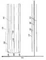
In certain embodiments, the layer ofOptical stack 16 is patterned to be parallel band, and can form the column electrode (further describing as follows) in the display device.The series of parallel band (and column electrode quadrature of 16a, 16b) thatremovable reflection horizon post 18 with formation and is deposited on the row on the top of the intervention expendable material between the post 18.When said expendable material when etching away,removable reflection horizon Optical stack gap 19 defined.For example the high conductivity of aluminium and reflective material can be used forreflection horizon 14, and these bands can form the row electrode in the display device.Notice that Fig. 1 maybe be not in scale.In certain embodiments, the spacing between thepost 18 can be approximately 10-100um, andgap 19 can about<1000 dusts.
As in Fig. 1, explaining throughpixel 12a, do not applying under the voltage condition,gap 19 keeps being betweenremovable reflection horizon 14a and theOptical stack 16a, and whereinremovable reflection horizon 14a is under the mechanical relaxation state.Yet when a current potential (voltage) difference being applied to through the row selected and row, in the charging that becomes of the capacitor of the column electrode at the pixel place of correspondence and the intersection formation of row electrode, and electrostatic force is moved electrode together to.If voltage is enough high, thenremovable reflection horizon 14 is out of shape and is pressed against on the Optical stack 16.Dielectric layers in the Optical stack 16 (undeclared among this figure) can prevent the separation distance between short circuit and key-course actuate pixel 12b explanation.Said behavior is identical, and irrelevant with the polarity of the potential difference (PD) that applies.
Fig. 2 is used for using in display application the example procedure and the system of interferometric modulator array to Fig. 5 explanation.
Fig. 2 can incorporate the system chart of an embodiment of the electronic installation that interferometric modulator is arranged into for explanation.Said electronic installation comprisesprocessor 21; It can be any general purpose single-chip or multicore sheet microprocessor; For example; ARM , Pentium
 , 8051, MIPS
 , Power PC
 or ALPHA
 ; Or any special microprocessor; For example, digital signal processor, microcontroller or programmable gate array.Like the convention of this technology,
processor 21 can be through being configured to carry out one or more software modules.Except that executive operating system, processor also can comprise web browser, telephony application, e-mail program or any other software application through being configured to carry out one or more software applications.


In one embodiment,processor 21 is also communicated by letter witharray driver 22 through being configured to.In one embodiment,array driver 22 comprisesrow driver circuits 24 and the column driver circuit 26 that signal is provided to array of display or panel 30.Row driver circuits and column driver circuit 26 can be generally known as section drive circuit and common actuator circuit, and can use the row or row in any one apply section voltage and common voltage.In addition, term " section " reaches " jointly " and only is used as mark in this article, and not set reception and registration exceeds any certain sense about the configuration of array of the meaning discussed among this paper.In certain embodiments, common line is extended along travelling electrode, and the section line extends along the fixed electorde in the Optical stack.The xsect of array illustrated in fig. 1 is to show by the line 1-1 among Fig. 2.Note; Though for clarity; Fig. 2 explains 3 * 3 arrays of interferometric modulator; But array ofdisplay 30 can contain a large amount of interferometric modulators, and the number of the interferometric modulator in being expert at can be different from the number (for example, 300 pixels of every row are taken advantage of 190 pixels of every row) of the interferometric modulator in row.
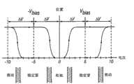
Fig. 3 is the removable mirror position of an example embodiment of the interferometric modulator of Fig. 1 figure to the voltage that applies.For the MEMS interferometric modulator, OK/the row actuation protocol can utilize the hysteresis property of these devices, as illustrated in fig. 3.Interferometric modulator can need (for example) 10 volt potential difference to make displaceable layers be deformed to actuating state from relaxed state.Yet, when voltage when said value reduces, along with voltage drop is returned below 10 volts, said displaceable layers is kept its state.In the example embodiment of Fig. 3, displaceable layers just can be lax fully when voltage drops to below 2 volts.Therefore, have a voltage range (in instance illustrated in fig. 3, for about 3V to 7V), exist one to apply voltage window therein, said when applying in the voltage window device stably be under lax or the actuating state.This paper is referred to as " lag window " or " stability window ".
In certain embodiments, actuation protocol can be based on for example the 5th, 835, the drive scheme of the drive scheme of discussing in No. 255 United States Patent (USP)s.In some embodiment of these drive schemes; Array of display for hysteresis characteristic with Fig. 3; Can design row/row actuation protocol so that during the gating of being expert at; Pixel to be activated in the row of institute's gating is exposed to about 10 volts voltage difference, and pixel to be relaxed is exposed to the voltage difference near zero volt.Behind gating, make pixel be exposed to about 5 volts steady state (SS) or bias voltage difference, make it remain in capable gating and make under its any state that is in.In this example, after being written into, each pixel receives the potential difference (PD) in 3 volts to 7 volts " stability window ".When coming other line of addressing through the gating different rows; Owing to applying along alignment with by the change of desired mode addressing, can between value in the stable stability window and the value in negative stable window, switch the voltage on the alignment of gating not through the bias voltage of the row of gating.This characteristic makes pixel design illustrated in fig. 1 apply under the voltage conditions stable being under the state that is pre-existing in actuating or lax identical.Because each pixel of interferometric modulator is in actuating state or relaxed state all is the capacitor that is formed by fixing and mobile reflection horizon basically, thus can keep this steady state (SS) under the voltage in lag window, and almost inactivity dissipates.If the current potential that applies is fixed, then have basically no electric current and flow to said pixel.
Further describe as follows, in some applications, can be through crossing over the frame that row electrode set transmission data-signal set (each data-signal has a certain voltage level) produces image according to desired set the in first row through actuate pixel.Then horizontal pulse is applied to first column electrode, it activates the pixel corresponding to the data-signal set.Then change data-signal set to gather through actuate pixel corresponding to desired in second row.Then pulse is applied to second column electrode, it activates the suitable pixel in second row according to data-signal.The first row pixel does not receive the influence of second horizontal pulse, and remains in its state that during first horizontal pulse, is set to.In regular turn mode for this process of capable repetition of whole series to produce frame.Usually, constantly repeating this process through the speed with certain frame number of being wanted of per second uses new view data to refresh and/or upgrades frame.Can use the row that is used for the driving pixels array and row electrode to produce the various agreements of picture frame.
Fig. 4 and Fig. 5 explanation is used for a kind of possible actuation protocol of this drive scheme, and wherein said actuation protocol is used on 3 * 3 arrays of Fig. 2 and produces display frame.Fig. 4 explanation can be used for showing the one group of possible row and the row voltage level of pixel of the hysteresis curve of Fig. 3.In Fig. 4 embodiment, activate a pixel and relate to suitable row are set at-VBiasAnd suitable row is set at+Δ V, it can correspond respectively to-5 volts and+5 volts.Through suitable row are set at+VBiasReach suitable row is set at identical+Δ V (thereby on pixel, producing zero volt potential difference), realize relax pixels.Remain in those row of zero volt will going voltage, pixel stably is in its original no matter what state that is in, and is in+V with said rowBiasOr-VBiasIrrelevant.Also as illustrated in fig. 4, can use the opposite polarity voltage with above-mentioned voltage, for example, activate a pixel and can relate to suitable row are set to+VBiasAnd will suitably go and be set to-Δ V.In this embodiment, be set at-V through will suitably being listed asBiasAnd will suitably go be set at identical-Δ V (thereby produce zero volt potential difference) on pixel, realize discharging pixel.
Fig. 5 B shows a series of row of 3 * 3 arrays that are applied to Fig. 2 and the sequential chart of column signal, and said signal will cause demonstration illustrated among Fig. 5 A to arrange (being non-reflexive through actuate pixel wherein).Before the illustrated frame, said pixel can be in arbitrary state in writing Fig. 5 A, and in this example, and all row are in 0 volt and all row at first and are in+and 5 volts.Under these voltage condition that apply, all pixels all stably are in its existing actuating or the relaxed state.
In Fig. 5 A frame, pixel (1,1), (1,2), (2,2), (3,2) and (3,3) activated.For realizing this purpose, during be expert at 1 " line time ",row row 3 are set at+5 volts.This does not change the state of any pixel, because all pixels all remain in the 3-7 volt stability window.Then, through being raised to 5 volts and the pulse of returning zero volt again to row 1 gating from 0 volt.This actuating (1,1) and (1,2) pixel and lax (1,3) pixel.Other pixel in the array is unaffected.In order to setrow 2 on demand,row 2 are set at-5 volts androw 1 androw 3 are set at+5 volts.Then, the same strobe signal that is applied torow 2 is with actuate pixel (2,2) and relax pixels (2,1) and (2,3).Again, other pixel of array is unaffected.Throughrow 2 androw 3 being set at-5 volts androw 1 are set at+5 volts and setrow 3 similarly.Row 3 gating signals are setrow 3 pixels, shown in Fig. 5 A.After writing said frame, the row current potential is zero, and the row current potential can remain in+5 or-5 volts, and then display is stable at the layout of Fig. 5 A.Said same program can be used for the array of tens of or hundreds of row and row.In the general principle of above-outlined, can change widely in order to carrying out sequential, sequence and the voltage level that row and row activate, and above embodiment is merely instance, and can uses any actuation voltage method with system and method described herein.
Fig. 6 A and Fig. 6 B are the system chart of the embodiment of explanation display device 40.For instance,display device 40 can be honeycomb fashion or mobile phone.Yet various types of display device are also explained in the same components ofdisplay device 40 or its slight variation, for example TV and portable electronic device.
Thedisplay 30 ofexemplary display device 40 can be any one in the various displays, comprises like bistable display described herein.In other embodiments,display 30 comprises flat-panel monitor, for example, and plasma, EL, OLED, STN LCD or TFT LCD (as stated), or non-tablet display, for example, CRT or other pipe unit.Yet as described herein, in order to describe the purpose of present embodiment,display 30 comprises interferometric modulator display.
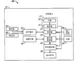
The assembly of an embodiment ofexemplary display device 40 schematically is illustrated among Fig. 6 B.Illustratedexemplary display device 40 comprisesshell 41, and can comprise the additional assemblies that at least partly is surrounded in it.For instance, in one embodiment,exemplary display device 40 comprisesnetwork interface 27, and saidnetwork interface 27 comprises theantenna 43 that is coupled totransceiver 47.Transceiver 47 is connected toprocessor 21, andprocessor 21 is connected to regulates hardware 52.Regulatinghardware 52 can be through being configured to conditioning signal (for example, signal being carried out filtering).Regulatehardware 52 and be connected toloudspeaker 45 andmicrophone 46.Processor 21 is also connected to inputmedia 48 and driver controller 29.Driver controller 29 is coupled toframe buffer 28 andarray driver 22, andarray driver 22 is coupled to array ofdisplay 30again.Power supply 50 is provided to all component by particularexemplary display device 40 designing requirement with electric power.
In an alternate embodiment,transceiver 47 can be replaced by a receiver.In another alternate embodiment,network interface 27 can be by a figure image source replacement, and the view data that is sent toprocessor 21 can be stored or produced to said figure image source.For instance, the figure image source can be digital video disk (DVD) or the hard disk drive that contains view data, or produces the software module of view data.
In one embodiment,processor 21 comprises that microcontroller, CPU or logical block control the operation of exemplary display device 40.Regulatehardware 52 and comprise amplifier and the wave filter that is used to transfer signals toloudspeaker 45 and is used for receiving signal substantially from microphone 46.Regulatehardware 52 and can be the discrete component in theexemplary display device 40, perhaps can be incorporated inprocessor 21 or other assembly.
Usually;Array driver 22 receives through formative information fromdriver controller 29; And video data is reformatted as one group of parallel waveform, said group of waveform many times is applied to the hundreds of and thousands of sometimes lead-in wires from the x-y picture element matrix of display by per second.
In one embodiment,driver controller 29,array driver 22 and array ofdisplay 30 are suitable for any kind display described herein.For instance, in one embodiment,driver controller 29 is conventional display controller or bistable state display controller (for example, interferometric modulator controller).In another embodiment,array driver 22 is conventional driver or bi-stable display driver (for example, interferometric modulator display).In one embodiment,driver controller 29 is integrated with array driver 22.This embodiment is common in the height integration system of for example cellular phone, wrist-watch and other small-area display.In another embodiment, array ofdisplay 30 is typical display array or bi-stable display array (display that for example, comprises interferometric modulator array).
As stated, in some embodiments, the control programmability is to be arranged in the driver controller at some places of electronic display system.In some cases, the control programmability is in the array driver 22.Above-mentioned optimization may be implemented in hardware and/or the component software of any number and in the various configurations.
CONSTRUCTED SPECIFICATION according to the interferometric modulator of the operate of above statement can change widely.For instance, Fig. 7 A explains five various embodiment of removable reflection horizon 14 and supporting construction thereof to Fig. 7 E.Fig. 7 A is the xsect of the embodiment of Fig. 1, and wherein strip of metal material 14 is deposited on the support member 18 of quadrature extension.In Fig. 7 B, the removable reflection horizon 14 of each interferometric modulator is being square or rectangle in shape and only on the corner on drift bolt 32, is being attached to support member.In Fig. 7 C, dangling for square or rectangle and from deformable layer 34 in shape in removable reflection horizon 14, and deformable layer 34 can comprise the flexible metal.Deformable layer 34 directly or indirectly is connected to substrate 20 around the periphery of deformable layer 34.These connections are known as support column in this article.Illustrated embodiment has support post plug 42 among Fig. 7 D, and deformable layer 34 is held on the said support post plug 42.Removable reflection horizon 14 keeps overhanging on the gap (like Fig. 7 A in Fig. 7 C), but deformable layer 34 does not form support column through the hole that is filled between deformable layer 34 and the Optical stack 16.On the contrary, support column is to be formed by smoothing material, and said smoothing material is in order to form support post plug 42.Illustrated embodiment is based on the embodiment that is showed among Fig. 7 D among Fig. 7 E, but also can be suitable for working with Fig. 7 A any person among the illustrated embodiment and the extra embodiment that does not show in Fig. 7 C.Among the embodiment that in Fig. 7 E, is showed, used the extra play of metal or other conductive material to form bus structure 44.This allows the back route signal along interferometric modulator, and it has been eliminated originally possibly must be formed at the some electrodes on the substrate 20.
In the embodiment of the for example embodiment shown in Fig. 7, interferometric modulator serves as the direct-view device, wherein inspects image from the front side of transparent substrates 20, said side and to be furnished with the side of modulator on it relative.In these embodiment, the part (comprising deformable layer 34) of the interferometric modulator on the side relative that reflection horizon 14 optics cover the reflection horizon with substrate 20.This allows under the situation that influences picture quality, to dispose not negatively and operate through shaded areas.For instance, this covers the bus structure 44 that allow among Fig. 7 E, said structure provide with the optical property of modulator and the electromechanical property of modulator (for example, addressing and by said addressing cause mobile) ability of separating.Structural design and the material that this discerptible modulator architecture allows to be used for dynamo-electric aspect and the optics aspect of modulator selected independently of one another and worked.In addition, Fig. 7 C has the optical property that derives from reflection horizon 14 and the additional benefit of its engineering properties decoupling zero to the embodiment shown in Fig. 7 E, and said engineering properties is realized by deformable layer 34.This structural design and material that allows to be used for reflection horizon 14 is able to optimization aspect optical property, and the structural design and the material that are used for deformable layer 34 are able to optimization aspect desired engineering properties.
In other embodiments, alternative drive scheme capable of using minimizes the required electric power of driving display, and permission common line to electromechanical assembly in the short period amount writes.In certain embodiments, for example the release of the electromechanical assembly of interferometric modulator or slack time comparable electromechanical assembly actuating time long do not activate or release conditions because maybe be only electromechanical assembly be moved to via the mechanical recovery force of displaceable layers.By contrast, the electrostatic force of actuator electric installation can act on the electromechanical assembly to cause the actuating of electromechanical assembly quickly.In the high voltage drive scheme of above argumentation, must be enough to not only allow the actuating of the previous electromechanical assembly that does not activate for the write time of alignment, and allow previous releasing to activate through the electromechanical assembly that activates.Therefore, in certain embodiments, the rate of release of electromechanical assembly is served as limiting factor, and it possibly suppress higher refresh rate is used for big array of display.
The alternative drive scheme that is called the low voltage drive scheme among this paper can provide the performance of comparing improvement with the drive scheme that applies bias voltage along common line and section line of above argumentation.Fig. 8 explains exemplary 2 * 3 array segment 100 of interferometric modulator, and wherein said array comprises three common line 110a, 110b and 110c and two section line 120a, 120b.Independent addressable pixel 130,131,132,133,134 and 135 is positioned at each intersection of common line and section line.Therefore, the voltage on the pixel 130 is poor between the voltage that puts on common line 110a and the section line 120a.This voltage difference on pixel alternatively is known as pixel voltage in this article.Similarly, pixel 131 is the intersection of common line 110b and section line 120a, and pixel 132 is the intersection of common line 110c and section line 120a.Pixel 133,134 and 135 is respectively the intersection of section line 120b and common line 110a, 110b and 110c.In illustrated example, common line comprises travelling electrode, and the electrode in the section line is the fixed part of Optical stack, but should be understood that in other embodiments the section line can comprise travelling electrode, and common line can comprise fixed electorde.Common voltage can be applied to common line 110a, 110b and 110c by common actuator circuit 102, and can section voltage be applied to section line 120a and 120b via section drive circuit 104.
In bi-chrome display, each among the pixel 130-135 can be identical in fact, has similar or identical electromechanical property.For instance; When electromechanical assembly is in the unactuated position; Gap between travelling electrode and the Optical stack can be identical in fact in the pixel each, and said pixel can have identical in fact actuating and release voltage and therefore identical in fact lag window.In color monitor, exemplary array section 100 can comprise the sub-pixel of three kinds of colors, and wherein each among the pixel 130-135 comprises the sub-pixel of a specific color.Color sub-pixel can make each common line 110a, 110b, 110c define the common line of the sub-pixel with similar color through arrangement.For instance; In the RGB display; Pixel 130 and 133 along common line 110a can comprise red sub-pixel, can comprise green sub-pixels along the pixel 131 and 134 of common line 110b, and can comprise blue subpixels along the pixel 132 and 135 of common line 110a.Though be depicted as three look displays, can in given color pixel, use any number subpixels.Therefore; 2 * 3 arrays can be represented two color pixel 138a and 138b in the RGB display; Wherein color pixel 138a comprises red sub-pixel 130, green sub-pixels 131 and blue subpixels 132, and color pixel 138b comprises red sub-pixel 133, green sub-pixels 134 and blue subpixels 135.
In other embodiments, use the sub-pixel of more or less kind of color, and correspondingly adjust the number of the common line of every pixel.In other embodiment again, can arrange the sub-pixel of an above color along single common line.For instance, in four look displays, 2 * 2 zones of display can form pixel, make that (for example)pixel 130 can be red sub-pixel, andpixel 133 can be green sub-pixels, andpixel 131 can be blue subpixels, andpixel 134 can be yellow sub-pixel.
In an embodiment who substitutes drive scheme, at high segment voltage VSHWith lower curtate voltage VSLBetween switch and to put on the voltage V onsection line 120a and the 120bSEGPut on the voltage V oncommon line
In a particular embodiment, high segment voltage VSHCan be low relatively voltage, approximately 1V-2V, and lower curtate voltage VSLCan be ground connection.Owing to high segment voltage and lower curtate voltage also are not in relation to the ground connection symmetry, the absolute value of therefore high maintenance and addressing voltage can be less than the absolute value (as seeing about (for example) Fig. 9 A after a while) of low maintenance and addressing voltage.Owing to being that pixel voltage is not only certain line voltage and is being controlled and activate,, but only need in the process of confirming suitable maintenance and addressing voltage, take in so this skew will can not influence the operation of pixel with disadvantageous mode.
For some electromechanical assembly, the positive lag window can be different with negative lag window, and can use along the offset voltage of common line and consider said difference.In this embodiment, when lower curtate voltage was set to ground connection, high and low maintenance voltage depended on high segment voltage VSHAnd the offset voltage V that can represent the INTRM intermediate point between positive lag value and the negative lagged valueOSAnd can represent the INTRM intermediate point and the offset voltage V of lag windowOSBetween the bias voltage V of differenceBIASSuitable high sustaining voltage can be provided by following formula
VCHOLD_H=1/2VSH-VOS+VBIAS
And suitable low maintenance voltage can be provided by following formula
VCHOLD_L=1/2VSH-VOS-VBIAS。
Can pass through extra voltage VADDBe added to high sustaining voltage and deduct V from the low voltage that keepsADDObtain high addressing voltage VCADD_HAnd low addressing voltage VCADD_LIt should be noted that can be through with 1/2 a Δ V (wherein Δ V representes poor between an any given height and the lower curtate voltage)replacement item 1/2VSHAnd more generally define said voltage to tackle the embodiment that low frequency voltage is not set at ground connection.In addition,, need sustaining voltage not placed the centre of lag window as discussing in more detail following, and through selecting to be used for VBIASThe comparable above exemplary values of discussing of value big or little.
Fig. 9 A explanation can put on the section line of Fig. 8 and the exemplary voltage waveform of common line, and Fig. 9 B explanation is in response to the gained pixel voltage on the pixel of Fig. 8 of the voltage that applies.Waveform 220a representes the time-varying section voltage that applies along thesection line 120a of Fig. 8, andwaveform 220b representes the section voltage that applies along sectionline 120b.Waveform 210a representes that the common voltage that applies along thealignment 110a of Fig. 8,waveform 210b represent the common voltage that applies alongalignment 110b, andwaveform 210c representes the common voltage that applies alongalignment 110c.Waveform 230 is illustrated in the pixel voltage on thepixel 130, and waveform 231-235 is illustrated in the pixel voltage on the pixel 131-135 respectively similarly.
In Fig. 9 A, can find out that each in the common line voltage starts from high retention value VCHOLD_H, for example, thehigh retention value 240a of waveform 220a.Applying this high retention value VCHOLD_HSome place during this time, the section line voltage (waveform 220a) ofsection line 120a is in lowercurtate voltage VS L250a, and the section line voltage (waveform 220a) ofsection line 120b is in high segment voltage VSH250b.Therefore, be directed against given VSEGParameter applies VCHOLD_HDuring this time,pixel 130 is exposed to maximum voltage difference, and in waveform 230 (betweenwaveform 210a and the 220a poor), can find out, this voltage difference on thepixel 130 does not move pixel voltage and exceeds negative actuation voltage 264.Similarly, be directed against given VSEGParameter applies VCHOLD_HDuring this time,pixel 133 is exposed to minimum voltage difference, and as can find out inwaveform 233 that the voltage on thepixel 133 does not move and exceeds the negative threshold value that discharges.Therefore, applying high sustaining voltage VC along the pixel 110 ofcommon line 110a and 113 state alongcommon line 110aHOLD_HKeep constant during this time, and irrelevant with the state of section voltage.
Common line voltage on thecommon line 110a (waveform 210a) then moves toground state 244a, and this causes along thepixel 130 ofcommon line pixel pixel 130 and 133.It may be noted that in this specific embodiment at this some place section voltage be lowercurtate voltage VS waveform
Common line voltage on theline 110a (waveform 210a) then moves to low retention value VCHOLD_L246a.When voltage was in low retention value 246, the section line voltage (waveform 210a) ofsection line 120a was in highsegment voltage VS H252a, and the section line voltage (waveform 210b) ofsection line 120b is in lower curtate voltage VSL250b.Voltage in thepixel positive release voltage 262 and arrives in the positive lag window, and is not moved beyondpositive actuation voltage 260, as can in thewaveform pixel
Then make the common line voltage (waveform 210a) on theline 110a be reduced to low addressing voltage VCADD_L248a.Pixel 130 and 133 behavior are looked current the section voltage that applies along its respective section line now and are decided.Forpixel 130, the section line voltage ofsection line 120a is in highsegment voltage VS H252a, and the pixel voltage increase ofpixel 130 exceedspositive actuation voltage 260, as can in thewaveform 230 of Fig. 9 B, finding out.Therefore this moment actuate pixel 130.Forpixel 133, pixel voltage (waveform 233) does not increase and exceeds positive actuation voltage, sopixel 133 keeps activating.
Next, will get back to thelow voltage 246a that keeps along common line voltage (waveform 210a) increase of line 110a.Like previous argumentation, low when keeping voltage 226a when applying, the voltage difference on the pixel keeps being in the lag window, and with the section independent from voltage.Voltage on the pixel 130 (waveform 230) therefore drops to positive actuation voltage below 260, but keeps being in positive release voltage more than 262, and therefore keeps through activating.Voltage on the pixel 133 (waveform 233) does not drop to positive release voltage below 262, and will keep not activating.
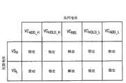
Figure 10 is for explaining the table of the pixel behavior that becomes with the voltage that puts on common line and section line.As can find out, apply release common voltage VCREL(pointing out that as above it can be ground state in many examples) will cause the release of pixel all the time, no matter section voltage is in high segment voltage VSHOr lower curtate voltage VSLSimilarly, apply sustaining voltage (VC along common lineHOLD_HOr VCHOLD_H) will make pixel be maintained at steady state (SS), and with the section voltage VS that appliesHOr VSLIrrelevant, and the pixel releasing that actuate pixel activates or warp activates is activated.When apply high addressing VC along common lineADD_HDuring voltage, can apply lower curtate voltage VS along the section lineLSo that activate, and can apply high segment voltage VS along other section line along the desired pixel of said common lineHSo that rest of pixels keeps not activating.When apply low addressing voltage VC along common lineADD_LDuring voltage, apply high segment voltage VSHWith the desired pixel actuating that makes along said common line, and lower curtate voltage VSLTo make pixel keep not activating.
In illustrated example, oncommon line 110b and 110c, apply similar common voltage, as can inwaveform waveform waveform 210a, but temporary transient respectively skew one and two line times.Because once only a common line is exposed to addressing voltage in this embodiment, so only said line will be written into, and the section voltage that during applying addressing voltage, applies is through selecting desired data are written to the current common line that just is being addressed.Also can find out, in the embodiment of Fig. 9 A and Fig. 9 B, carry out the whole releases and the ablation process of a given alignment at single line time durations.In other embodiments, a plurality of line times of the extensible leap of the part of this process will be as will discuss following in more detail.
In case addressing all common line, the initialcommon line 110a of addressing once more then begins to write the process of another frame.Can find out, in second ablation process (waveform 210a), use just keeping and addressing voltage the first common line 110a.Also can find out, write cycle period in negative polarity, when using low maintenance and addressing voltage, high segment voltage will cause along the actuating of the pixel of said section line.Similarly, write cycle period in positive polarity, lower curtate voltage will cause along the actuating of the pixel of said section line, and it will be big as much as possible (putting on the voltage difference between the voltage of common line and section line of said pixel) because the absolute value of pixel voltage.Because this meaning of the state of sector data (being known as " sensing " of data among this paper) in this embodiment one by one frame ground alternately, so must follow the tracks of the polarity of write-in program so that can suitably format to section voltage.
Can carry out a plurality of modifications to the low voltage drive scheme of above description.In the drive scheme of Fig. 9 A and Fig. 9 B, the purpose in order to simplify is set in 0V with offset voltage, but can use other suitable offset voltage.For instance, when common line during for the line of interferometric modulator with different electromechanical properties (for example, through being configured to reflect the sub-pixel of different color), actuation voltage, release voltage and offset voltage can be different.Therefore, comprise among the embodiment of sub-pixel of different color atcommon line
In addition, in other embodiments, section voltage can not change between lower curtate voltage and ground connection, and alternately between high segment voltage and lower curtate voltage (for example, positive section voltage and minus zone section voltage), changes.Equal in fact among the embodiment of absolute value of lower curtate voltage (under said situation, section voltage is the center with ground connection) at the absolute value of high segment voltage, just reaching negative keep and addressing voltage can be in fact about the offset voltage symmetry.In other embodiments, two section voltages can have identical polar, for example, high segment voltage are set to 2.5V and lower curtate voltage are set to 0.5 volt embodiment.Yet, in certain embodiments, the absolute value of section voltage is minimized the section driver is simplified.
In Fig. 9 A in the illustrated example, once write first frame through using a series of addressing voltages with identical polar that in the common line each is write.Then through using a series of addressing voltages with opposite polarity that in the common line each is write the polarity of once putting upside down second frame.Can continue end switch polarity at the write-in program of each frame.This frame is put upside down and can be helped to be equilibrated at the electric charge accumulation on the pixel of device through the polarity of write-in program alternately.Yet, in other embodiments, can before the end of the process that writes whole frame, put upside down polarity, for example, put upside down one by one line.In other embodiment (wherein each group comprises a common line of the interferometric modulator of specific color) that common line is arranged in the color group, can after each color group, change polarity.
The voltage signal that Figure 11 explanation can be used in thisembodiment.Voltage voltage 220a and the 220b about Fig. 9 A discusses like preceding text.Can applyvoltage 320a alongsection line 320a, and can applyvoltage 320b along section line 320b.Similarly, can applyvoltage common line
Can find out thatvoltage 310a at first comprises the write-in program of carrying out alongcommon line 110a with negative polarity.Subsequently, workingvoltage 310b carries out the write-in program with positive polarity along common line 110b.The polarity of write-in program continues one by one, and line ground replaces.In the illustrated embodiment, because there is the odd number common line, so the polarity of the write-in program of carrying out along a given common line also will replace in time.In the embodiment that has the even number common line, can be with to the polarity of the write-in program of last common line polarity, so that keep alter polarity along given common line with next write-in program of first common line of opposing.Perhaps, but the polarity of specific write-in program (for example, the first-line write-in program in the frame) is selected on pseudorandom ground.The polarity of the write-in program subsequently in the said frame one by one line or one by one color group ground alternately, or himself can be selected by pseudorandom ground.
Put upside down among the embodiment at the line of Figure 11, the sensing of data one by one line but not one by one frame ground change, but still can follow the tracks of the current polarity that writes voltage in a similar manner, and said polarity can be in order to suitably confirm will be along the data-signal of section line transmission.
In a further embodiment, can revise the low voltage drive scheme causes addressing voltage is put at least some in the step of the common line different with the common line of current positive addressing with execution.In a particular embodiment, make and discharge and write-in program extends across a plurality of line times and can allow the refresh rate faster of display.Can not cause not activating interferometric modulator (irrelevant) because be different from all voltages of the voltage that is used for high and low addressing voltage through being chosen as with addressing voltage; So can section voltage be set to appropriate value writing data into the common line of current positive addressing, and not influence along the state of the pixel of other common line.
Figure 12 explains the embodiment that carries out release and write-in program at three lines in the time.In one embodiment, be released in the common line of current two lines in line front that just are being written into, and will move to suitable sustaining voltage in the common line of the current line in line front that just is being written into.However, it should be understood that can be by arbitrary suitable order addressing common line, and as formerly show in the illustrated example, do not need addressing common line in regular turn.
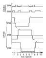
Figure 12 describes the waveform that expression can put on the voltage on three different common line (for example,common line waveform 410b representes to put on the voltage of the common line with green sub-pixels, and waveform 410c representes to put on the voltage of the common line with blue subpixels.Except based on the possible difference of the suitable offset voltage of the interferometric modulator of different color and bias voltage and revise the value of sustaining voltage and release voltage, also can change other parameter ofwaveform
In thefirst line time 470 illustrated in fig. 12, can find out that in the duration ofline duration 470,waveform 410a is in ground state 444a.As can find out that these waveforms can keep being in ground state best in greater than the time span of single line time about waveform 410b.Through in the time longer, on common line, applying ground voltage, can guarantee to have the release of the interferometric modulator of the release time longer than actuating time than the single line time.In other embodiments, high sustaining voltage and low keep transformation between the voltage can cause in the time enough amount, being applied in the release window of pixel voltage so that device discharge.Therefore, in certain embodiments, need in the specific time cycle, on alignment, not apply the for example fixedly release voltage ofvoltage 444a.
In thesecond line time 471,voltage 410a is increased to high retention value 440a.Voltage will not cause any one the actuating in the interferometric modulator because be increased tohigh retention value 440a, so need not remain onhigh retention value 440a in the same long time being inground connection value 444a with itsmaintenance.Voltage 410b remains onground state 444b during thisline time 471, and voltage 410c is increased to ground state 444c from low maintenance state 446c.
In the three-way time 472, sufficient to guarantee set activated along all pixels ofcommon line 110a with the time cycle that activated in,voltage 410a is increased to high addressing oroverdrive voltage 442a from high sustaining voltage 440a.Therefore carry out the positive polarity write-in program, wherein the position is that arbitrary pixel along the section line that has applied lower curtate voltage will activated incommon line 110a, and the position is that arbitrary pixel along the section line that has applied high segment voltage will keep actuating.Then voltage is rolled back high sustainingvoltage 440a downwards.In this line time 472,voltage 410b is reduced tolow maintenance voltage 446b, and voltage 410c remains on ground state 444c.
In the4th line time 473, carry out the negative polarity write-in program alongalignment 110b, whereinvoltage 410b is reduced to low addressingvoltage 448b from thelow voltage 446b that keeps in the time cycle of the desired pixel ofcommon line 110b being enough to activate.
In the 5th line time 474, to carry out the positive polarity write-in program along alignment 110c with the above similar mode of discussing about the positive polarity write-in program of in the three-way time 472, carrying out of mode alongalignment 110a.
Therefore, even complete release and write-in program are crossed over a plurality of line times, when section voltage when suitably selecting, the applying of release procedure and sustaining voltage also to influence pixel with the consistent mode of section independent from voltage.Therefore can these programs be applied to arbitrary desired common line, and with the data independence that just is being written to common line at the certain line time durations.Function that the line time is merely the write time is activated guaranteeing, but not also be the function of release time.
Point out that as above the suitable selection of magnitude of voltage is useful.Actuating and release voltage as the interferometric modulator of different color can change, and manufacturing variation or other factors can cause the interferometric modulator of same color to have activating or a certain difference of release voltage.Therefore can actuation voltage and release voltage be handled as little voltage range.Also can suppose a certain error allowance, and with it in order to the buffering between the expectation value that defines various voltages.Just to reach Fig. 3 of negative voltage range opposite with explanation, and Figure 13 explains the scope of the voltage that can apply in the various times of main leap positive voltage.
Can find out that in Figure 13 the minimum value of voltage swing Δ VS can be provided by the variation of actuation voltage.Because voltage swing Δ VS is identical for just reaching negative write-in program in certain embodiments, therefore just reaching the minimum value that the greater in the variation of negative actuation voltage can be Δ VS.In addition, because Δ VS is identical in the common line of the sub-pixel that different color is arranged each in certain embodiments, therefore has the minimum value of the subpixel colors may command voltage swing Δ VS that the maximum of actuating time changes on the said array.In certain embodiments, in the process of confirming various voltages, utilize extra buffer value to avoid unintentional actuating to pixel.
Actuating time is also looked addressing voltage (perhaps being known as overdrive voltage, as noted before) and is decided, because the addressing voltage that increases will be increased to the speed of the flow of charge of interferometric modulator, acts on the electrostatic force on the displaceable layers thereby increase.In particular, if make the distance between the foreign range of addressing voltage and actuation voltage bigger,, can increase the actuating time of pixel then owing to increase by all electrostatic force of experiencing through the pixel of addressing.If can make the actuation voltage window as much as possible little, then can guarantee that in the pixel each will experience extra electrostatic force, and can therefore reduce the line time for given voltage swing.
Point out that as above for example the use of the low voltage drive scheme of the above low voltage drive scheme of discussing can provide many advantages of comparing with the high voltage drive scheme.A significant advantage is the power consumption of minimizing as a rule.Under the high voltage drive scheme, " manifesting (rip) " or the required energy of reproduced image are looked the present image on the array of display and are decided, and by section voltage is switched to the required energy control of its set value from its preceding value.Because the switching of the section voltage in the high voltage drive scheme usually need be in the switching between positive bias voltage and the negative bias voltage, so the section voltage swing is approximately roughly 12 volts (supposition is 6 volts bias voltages roughly).By contrast, the section voltage swing in the low voltage drive scheme can be approximately roughly 2 volts.Therefore manifest the required energy of image by up to (2/12)2The factor reduce, thereby have significant energy-efficient.
In addition, use low-voltage to reduce the risk that is coupled to unintentional pixel switching of common line owing to the section signal along the section line.Reduce the amplitude and the duration of any spur signal (spurious signal) that produces by crosstalking, thereby reduced the possibility that wrong pixel is switched.This has also reduced the constraint to the resistance in whole array and the periphery, thereby allows to use material and the design with high electrical resistance, or in the periphery of array, uses narrower wiring.
But also increased the scope of the working voltage in the lag window.Because the high voltage drive scheme of above argumentation can intentionally should not be crossed over the pixel releasing that will activate when two continuous frames keep through actuating in pixel and activated and activate again, so must avoid unintentional actuating of pixel.Use can enough alleviate this problem through guaranteeing the switching between positive lag value and negative lagged value soon than the remarkable high bias voltage of DC release voltage, but just spendable bias voltage is restricted to the little and view picture than DC lag window thus and in the fixed quickflashing biasing window (flash bias window).By contrast, because in the low voltage drive scheme, before activating again, each pixel was released in cycle time, so unintentional release is not problem, and can use whole DC lag window.
Low-voltage area segment driver circuit also can reduce the cost of drive circuit.Because therefore employed low voltage can build through DLC(digital logic circuit) and put the section drive circuit.This can be specially adapted to have the big panel of a plurality of integrated circuit that drive panel.In the common actuator circuit, introduced a certain extra complicacy, because the common actuator circuit is through being configured on given common line five different voltages of output, but this complicacy is remedied by the simplification of section drive circuit.
That low voltage drive device circuit also permits using is less, interferometric modulator pixel faster.For less interferometric modulator element, it is unrealistic that the high voltage drive scheme can become.For instance, part when using the high voltage drive scheme, uses the interferometric modulator possibility of the spacing below 45 μ m spacings or the 45 μ m unrealistic owing to the actuation speed of the pixel that possibly discharge too fastly.By contrast, when using the low voltage drive scheme of the drive scheme of discussing among this paper for example, the interferometric modulator of the spacing below 38 μ m spacings or the 38 μ m is spendable.
Also can reduce the line time of interferometric modulator significantly.Use the high voltage drive scheme possibly be difficult on display, realize the line time, but when using the low voltage drive scheme less than 100 μ s, less than line time of 10 μ s be possible.In certain embodiments, line time decreased that can the low voltage drive scheme is required is written into the point of twice (once use positive polarity, and once use negative polarity) to the content in given frame.This pair ablation process is desirable charge balance process, because it does not depend on the probability of the charge balance on a large amount of frames.On the contrary, through writing with positive polarity and negative polarity, in each frame, each pixel is a charge balance.
As can in (for example) Figure 13, find out; Pixel remains on steady state following time with regard to activating during applying sustaining voltage; Owing to the section voltage that on the section line of correspondence, applies alternately, the institute's voltage that applies on the pixel can constantly replace between two voltages in lag window.When pixel is in not actuating state, confirm the position of displaceable layers based on the position that mechanical recovery force is equated with the electrostatic force that is produced by the pixel voltage difference.Because the color by the interferometric modulator reflection becomes with the position of displaceable layers with respect to Optical stack, the color that this change in location can cause being reflected by the interferometric modulator under actuating state is two variations that do not activate between the color.
In having the embodiment that frame puts upside down, the constant polarity of crossing over the zone of array in given image duration can cause certain obvious flicker of section line, because given section voltage will influence the nearly all not actuate pixel along the section line in the same manner.In certain embodiments; The line of the type of more than discussing is put upside down and can be alleviated this flicker; Because can receive the influence of the opposite way of given section voltage, possibly show as the much meticulous visual pattern that does not activate with two that the color state is blended together thereby produce along the neighborhood pixels of section line.In other embodiments, can intentionally switch section voltage to guarantee that actuate pixel does not spend its half the time in two each that do not activate in the color state at each line time durations.
Refreshing fast of display can take place during the demonstration of video or similar dynamic content, makes after having accomplished former frame, just to write next frame immediately or soon.Yet, in other embodiments, through in cycle time, applying sustaining voltage on each in common line, show particular frame in the time cycle of prolongation that can be after writing incoming frame.In certain embodiments, this is attributable to the demonstration of relative still image (for example, the GUI of mobile phone or other display).In other embodiments, the number of the common line in the display can be enough little (special in having slow refresh rate or the embodiment of short-term time) so that the write time of frame is significantly shorter than the demonstration time of frame.In other embodiments, the operation of specific GUI or out of Memory show possibly be only required in the part of refresh display in the given frame, and does not need other part of the said display of addressing.
In one embodiment, can avoid or alleviate flicker through during the cycle between at this moment section voltage being maintained constant voltage.In a particular embodiment, in the section voltage each is maintained identical voltage, said voltage can be high segment voltage, lower curtate voltage or intermediate value voltage.In other embodiments, can voltage be maintained in order to write data into the voltage of last common line.Yet, through on all section lines, keeping constant voltage, can be provided at the big homogeneity of color on the whole color monitor because each of given color not actuate pixel will have the pixel voltage that is similarly applied.
Figure 14 explanation writes the embodiment of the displaying scheme of themaintenance sequence 580 that has prolongation after 570 at frame.Putting on common line voltage on first alignment (for example, thecommon line 110a of 2 * 3 arrays of Fig. 8) writes 570 end at frame and is in high sustainingvoltage 540a (seeingwaveform 510a).Similarly; Put on common line voltage on second alignment ofcommon line 110b for example and write 570 end at frame and be in thelow voltage 546b (seeingwaveform 510b) of maintenance, and the common line voltage that puts on the 3rd common line of common line 110c for example is in high sustaining voltage 540c.
The section voltage that puts on the section line (for example, thesection line 120a and the 120b of the array of Fig. 8) changes (seeingwaveform high segment voltage lower curtate voltage 552a, 552b.Can find out thatsection voltage waveform
Write 570 end at frame, the voltage (seeingwaveform 520a) that puts on thesection line 120a moves tointermediate value voltage 554a, and the voltage (seeingwaveform 520b) that puts on thesection line 120b moves to intermediate value voltage 554b.As above mentioned; Section voltage alternately moves to high or low section voltage or arbitrary other voltage; But during the hold mode ground connection is being meaned that as section voltage pixel voltage on given pixel will equal the common line voltage that applies along the common line of correspondence in fact, this can simplify confirming desired sustaining voltage in other embodiments.Apply even voltage through in the section line each, the pixel voltage on the not actuate pixel on the given common line will equate.When putting on similar sustaining voltage on a plurality of common line, all with given sustaining voltage that is applied the not pixel voltage of actuate pixel will equate.
Therefore; In having the RGB display of red, green and blue common line; Can exist in six distinct sustaining voltages that apply during themaintenance sequence 580 of prolongation: high and low red sustaining voltage, high and low blue sustaining voltage, and high and low green sustaining voltage.Apply uniform section voltage through in the section line each, therefore the pixel voltage on the not actuate pixel in array will be one in six probable values (two values of each color).By contrast, if on various section lines, apply height and lower curtate voltage both, then can have 12 kinds of possible pixel voltages, this is attributable to the variation of the position of actuate pixel not and causes the marked change by the color of interferometric modulator array reflection.
In other embodiment, also can be along the sustaining voltage of common line through adjustment to consider this effect.In one embodiment, be used at least one of low and high sustaining voltage of a given color can be through adjustment so that be in the pixel under said height and the low-voltage pixel voltage absolute value each other near.If the absolute value of pixel voltage is equal to each other in fact, then given color all not actuate pixel will reflect same hue in fact, thereby be provided at the color uniformity preferably on the whole display.In addition, for the purpose of white balance, can make the sustaining voltage optimization of the various colors in multicolor display (for example, the RGB display), feasible combined reflected color by redness, green and blue pixel is in specific white point so that desired white balance to be provided.
In other embodiments, can adjust the height that is used for given color and low keep voltage both so that desired pixel voltage to be provided.For instance, possibly require the specific red tone of specific pixel voltage, and can make height and both optimizations of low-voltage so that desired pixel voltage to be provided when putting on constant section voltage on the section line.
When applying the section voltage of fluctuation, sustaining voltage is limited to the voltage that when applying the highest or minimum section voltage, will not cause the actuating or the release of pixel.By contrast, when the section voltage constant that applies, do not need this allowance, therefore increased and to have applied and do not change the scope of possible sustaining voltage of the state of pixel along common line.In particular, can use near the actuating of pixel and the sustaining voltage of release voltage.In certain embodiments, can be chosen in the voltage in this extra available voltage range to sustaining voltage.
In certain embodiments, can be be used for sustaining voltage (even frame write cycle during) through the sustaining voltage of optimizing.Yet,,, can use and can not write the sustaining voltage of using during 570 at frame in case therefore frame writes 570 end and just applying constant section voltage owing to can during thehold period 580 that prolongs, the voltage range as sustaining voltage increase.This of sustaining voltage writes back (post-write) adjustment and is illustrated among Figure 14, and wherein the voltage on thecommon line 110a (waveform 510) is increased to the sustaining voltage 549a through optimizing from high sustaining voltage 540a.Similarly, the voltage on thecommon line 110b (waveform 510b) is increased to the sustaining voltage 549b through optimizing from the low voltage 446a that keeps, and the voltage on the common line 110c (waveform 510c) is reduced to the sustaining voltage 549c through optimizing from high sustaining voltage 540c.
The variation of the sustaining voltage of suitable warp optimization with the consideration manufacture process confirmed on panel ground one by one.Through measuring the characteristic (for example, the electric capacity of interferometric modulator) of interferometric modulator, can confirm to provide the suitable pixel voltage and the sustaining voltage of desired optic response.
In other embodiments, even can in the display of the hold period that do not have to prolong, make sustaining voltage optimization.Because in given embodiment, possibly exist the adjustment sustaining voltage to guarantee simultaneously to be in a certain space in the lag window, so the minimized sustaining voltage of visual effect of this variation of position that can select to make displaceable layers is as sustaining voltage when the maintenance of pixel voltage when common line applies sustaining voltage.For instance, can select bias voltage so that the different tones of same color are reflected in two holding positions of the interferometric modulator that does not activate, but not in said state one in shift to another color.
Be susceptible to the above embodiment of above argumentation and the various combinations of method.In particular, though above embodiment in other embodiments, alternately arranges the interferometric modulator of specific color mainly to the embodiment that arranges the interferometric modulator of particular element along common line along the section line.In a particular embodiment, can the different value of height and lower curtate voltage be used for specific color, and can apply identical maintenance, release and addressing voltage along common line.In a further embodiment; When the sub-pixel that makes multicolour (is for example located along common line and section line; The four look displays of more than discussing) time; Can be along common line with the use that combines with the different value of maintenance and addressing voltage of the different value of height and lower curtate voltage, so that suitable pixel voltage is provided in four colors each.The method of the test of describing among this paper in addition, can be used with other method combination of driving machine electric installation.
Also will be appreciated that; Only if this paper has specific and clearly statement in addition; Otherwise look embodiment and decide; The action of any method of describing among this paper or incident can be carried out by other sequence, can be added, merge or save fully (for example, be not everything or incident are put into practice said method necessary).
Though the novel feature that is applicable to various embodiment has been showed, described and pointed out to above detailed description, can carry out form and various omissions, replacement and the change of details of the device of illustrated process.Can make does not provide all characteristics of stating among this paper and some forms of benefit, and some characteristics can be used with further feature or put into practice dividually.
Claims (63)
1. the method for a driving machine array of electrical devices, said method comprises:
Electromechanical assembly in the said array is carried out the actuating operation, and each actuating operation of wherein said electromechanical assembly being carried out comprises:
On said electromechanical assembly, apply release voltage, wherein said release voltage keeps being between the negative release voltage of positive release voltage and said electromechanical assembly of said electromechanical assembly; And
On said electromechanical assembly, apply addressing voltage, wherein said addressing voltage is greater than the positive actuation voltage of said electromechanical assembly or less than the negative actuation voltage of said electromechanical assembly.
2. method according to claim 1, wherein said release voltage changes between less than the high voltage of the positive release value of said electromechanical assembly and the low-voltage greater than the negative release value of said electromechanical assembly.
3. method according to claim 1, wherein each activates to operate further to be included on the said electromechanical assembly and applies sustaining voltage, and wherein said sustaining voltage keeps being in the lag window of said electromechanical assembly.
4. change between the low-voltage in the said same lag window of method according to claim 3, wherein said sustaining voltage high voltage and the said electromechanical assembly in the lag window of said electromechanical assembly.
5. method according to claim 1, wherein said electromechanical assembly array comprises interferometric modulator array.
6. method according to claim 1, it comprises extraly second electromechanical assembly carry out is activated operation, and wherein said method comprises simultaneously release voltage is applied to said second electromechanical assembly and addressing voltage is applied to said first mechanical hook-up.
7. display that comprises a plurality of dynamo-electric display elements, said display comprises:
Dynamo-electric display component array; And
Drive circuit, it is through being configured to that the electromechanical assembly in the said array is carried out the actuating operation, and each actuating operation of wherein said electromechanical assembly being carried out comprises:
On said electromechanical assembly, apply release voltage, wherein said release voltage keeps being between the negative release voltage of positive release voltage and said electromechanical assembly of said electromechanical assembly; And
On said electromechanical assembly, apply addressing voltage, wherein said addressing voltage is greater than the positive actuation voltage of said electromechanical assembly or less than the negative actuation voltage of said electromechanical assembly.
8. display according to claim 7, wherein said drive circuit is through further being configured to after applying said addressing voltage, on said electromechanical assembly, apply sustaining voltage, and wherein said sustaining voltage keeps being in the lag window of said electromechanical assembly.
9. change between the low-voltage in the said same lag window of display according to claim 8, wherein said sustaining voltage high voltage and the said electromechanical assembly in the lag window of said electromechanical assembly.
10. display according to claim 7, wherein said release voltage changes between less than the high voltage of the positive release value of said electromechanical assembly and the low-voltage greater than the negative release value of said electromechanical assembly.
11. display according to claim 7, wherein said drive circuit are applied to release voltage the second dynamo-electric display element and addressing voltage are applied to said dynamo-electric display element simultaneously through being configured to.
12. display according to claim 7, wherein said array comprise a plurality of interferometric modulators of first color and a plurality of interferometric modulators of second color.
13. display according to claim 12; Wherein said electromechanical compo comprises the interferometric modulator of said first color; And wherein second electromechanical compo comprises the interferometric modulator of second color, and wherein said drive circuit is applied to release voltage the second dynamo-electric display element and addressing voltage is applied to said dynamo-electric display element simultaneously through being configured to.
14. the method for the electromechanical assembly in the driving machine array of electrical devices, said electromechanical assembly comprises first electrode with section line electrical communication, said first electrode with open with second electrode gap of common line electrical communication, said method comprises:
On said section line, apply section voltage, wherein said section voltage changes between maximum voltage and minimum voltage, and the difference between wherein said maximum voltage and the said minimum voltage is less than the width of the lag window of said electromechanical assembly;
On said common line, apply resetting voltage, wherein said resetting voltage is through being configured to said electromechanical assembly placed not under the actuating state; And
On said common line, apply overdrive voltage, wherein said overdrive voltage is through being configured to based on the state of said section voltage said electromechanical assembly to be activated.
15. method according to claim 14, it is included in extraly on the said common line and applies sustaining voltage, and wherein said sustaining voltage maintains said electromechanical assembly under its current state through being configured to, and irrelevant with the said state of said section voltage.
16. method according to claim 15 wherein applies said sustaining voltage after applying said resetting voltage and before applying said overdrive voltage.
17. method according to claim 15 wherein applies said sustaining voltage after applying said overdrive voltage.
18. method according to claim 17; It is included in extraly and applies after the said resetting voltage and second sustaining voltage before applying said overdrive voltage; Wherein said first sustaining voltage is in first lag window of said electromechanical assembly, and wherein said second sustaining voltage is in second lag window of said electromechanical assembly.
19. method according to claim 18; Wherein apply resetting voltage and be included in and apply the voltage that changes to said second sustaining voltage from said first sustaining voltage on the said common line, said voltage kept being in the release window of said electromechanical assembly in the time cycle of the release that is enough to cause said electromechanical assembly.
20. method according to claim 15, the absolute value of wherein said overdrive voltage is greater than the absolute value of said sustaining voltage.
21. method according to claim 15, wherein said sustaining voltage is positioned at the lag window of said electromechanical assembly.
22. the method for a driving machine array of electrical devices; Said array comprises a plurality of common line and a plurality of section line; Each electromechanical assembly comprises first electrode with the common line electrical communication, said first electrode with open with second electrode gap of section line electrical communication, said method comprises:
Apply section voltage in said a plurality of section lines each, the said section voltage that wherein puts on the given section line can switch between high segment voltage status and lower curtate voltage status; And
Applying release voltage on first common line and on second common line, applying addressing voltage simultaneously; Wherein said release voltage causes along all of said first common line through the release of the electromechanical assembly that activates and irrelevant with the said state of the section voltage that is applied to each electromechanical assembly, and wherein said addressing voltage is looked said the state of the said section voltage that is applied to given electromechanical assembly and caused the actuating of electromechanical assembly surely.
23. method according to claim 22 wherein applies said addressing voltage on said second common line after the release of the electromechanical assembly that any warp along said second common line location activates.
24. method according to claim 22; It applies sustaining voltage after being included in extraly and applying said addressing voltage on said second common line; Wherein said sustaining voltage will maintain under its current state along the said electromechanical assembly of said second common line, and irrelevant with each the said state of said section voltage that is applied in the said electromechanical assembly.
25. method according to claim 22, wherein said array comprise through being configured to more than first electromechanical assembly of reflection first color in actuated position, reach through being configured to more than second electromechanical assembly of reflection second color in actuated position.
26. method according to claim 25, wherein said more than first electromechanical assembly are arranged along first common line, and wherein said more than second electromechanical assembly arranged along second common line.
27. method according to claim 26; The said addressing voltage that wherein puts on said first common line is first addressing voltage; The said addressing voltage that wherein puts on said second common line is second addressing voltage, and wherein said first addressing voltage is different with said second addressing voltage.
28. method according to claim 25, wherein said more than first electromechanical assembly are arranged along the first section line, and wherein said more than second electromechanical assembly arranged along the second section line.
29. method according to claim 28; The said section voltage that wherein puts on the said first section line changes between the first high segment voltage and the first lower curtate voltage; The said section voltage that wherein puts on the said second section line changes between the second high segment voltage and the second lower curtate voltage, and the wherein said first high segment voltage is different with the said second high segment voltage.
30. a display device, it comprises:
Electromechanical assembly array, said array comprise a plurality of common line and a plurality of section line, and each electromechanical assembly comprises first electrode with the common line electrical communication, said first electrode with open with second electrode gap of section line electrical communication; And
Drive circuit; It is through being configured on the section line, to apply high segment voltage and lower curtate voltage; And through being configured on common line, to apply release voltage and addressing voltage, wherein said drive circuit applies release voltage and applies addressing voltage along second common line along first common line through being configured to the while;
Wherein said high segment voltage and said lower curtate voltage through selecting so that said release voltage discharges along the electromechanical assembly of common line location with the said section independent from voltage that applies, and said addressing voltage is looked said the section voltage that applies and fixed causing along the actuating of the specific electromechanical assembly of common line.
31. display device according to claim 30; Wherein said drive circuit is through further being configured on common line, apply sustaining voltage; Wherein said sustaining voltage will maintain under its current state along the said electromechanical assembly of common line, and with the said section independent from voltage that applies.
32. display device according to claim 31, wherein said drive circuit is through being configured to apply one in release voltage, high sustaining voltage, high addressing voltage, low maintenance voltage and the low addressing voltage.
33. display device according to claim 32, wherein given electromechanical assembly activate after being to apply said high addressing voltage on the corresponding common line and on the section line of correspondence, applying said lower curtate voltage.
34. display device according to claim 32, wherein given electromechanical assembly activate after being to apply said low addressing voltage on the corresponding common line and on the section line of correspondence, applying said high segment voltage.
35. display device according to claim 31, wherein said drive circuit is through further being configured to when no addressing voltage is applied on any common line, identical section voltage put on each in the said section line.
36. display device according to claim 31; Wherein said drive circuit is through further being configured to when no addressing voltage is applied on any common line, to apply the sustaining voltage through optimizing, and wherein said sustaining voltage through optimization maintains the electromechanical assembly of not actuating in the desired unactuated position through being configured to.
37. display device according to claim 36, wherein said is that part is selected based on the gained white balance of said array when applying said sustaining voltage through optimization at least through the sustaining voltage of optimizing.
38. display device according to claim 36, wherein said sustaining voltage through optimization is different with said sustaining voltage.
39. the method for the electric charge in the equilibrator array of electrical devices, said array comprises a plurality of section lines and a plurality of common line, and said method comprises:
Said common line is carried out write operation, wherein carries out write operation and comprise:
At least part selects to be used for the polarity of said write operation based on the charge balance criterion;
Carry out reset operation through on common line, applying resetting voltage, each that said resetting voltage will be in the said electromechanical assembly of common line places not under the actuating state;
On said common line, apply the sustaining voltage with said selected polarity, wherein said sustaining voltage can not make any one actuating in the said electromechanical assembly of said common line; And
Side by side applying overdrive voltage on the said common line and on said section line, applying a plurality of section voltages with said selected polarity; Wherein said section voltage changes between first polarity and second polarity, and wherein when the said polarity of said overdrive voltage and the said polarity of corresponding section voltage are inequality said overdrive voltage cause the said actuating of electromechanical assembly.
40. according to the described method of claim 39, the polarity of wherein selecting to be used for the said write operation comprises the said polarity of the alternately write operation on said common line.
41. according to the described method of claim 39, the polarity of wherein selecting to be used for the said write operation comprises with pseudo-random fashion selection polarity.
42. according to the described method of claim 41; The polarity of wherein selecting to be used for the said write operation with pseudo-random fashion comprises the polarity of selecting to be used for first common line with pseudo random pattern, and said method further comprises based on the said selected polarity of said first common line confirms to be used for the polarity in the write operation subsequently of frame.
43. a method that drives display component array, said method comprises:
Voltage waveform is applied at least a portion of display component array; Said voltage waveform comprises frame and writes waveform and keep sequence waveform; Sizable number percent that wherein said frame writes waveform has the value that equals release voltage, high or low sustaining voltage or high or low addressing voltage in fact, and sizable number percent of wherein said maintenance sequence waveform comprises different with the said high or low sustaining voltage in fact sustaining voltages through adjustment.
44. according to the described method of claim 43, wherein said through the adjustment sustaining voltage be based in the said display element at least one electric capacity and be scheduled to.
45. according to the described method of claim 43, wherein said sustaining voltage warp through adjustment is predetermined so that desired optic response is provided.
46. according to the described method of claim 43, wherein said sustaining voltage warp through adjustment is predetermined so that desired white balance is provided.
47. according to the described method of claim 43, it further comprises the cross section that the section voltage waveform is applied to said array, the said cross section of said array part is at least overlapped with the said of said array.
48. according to the described method of claim 47; Wherein said section voltage waveform comprises the section frame and writes waveform and section maintenance sequence waveform; Sizable number percent that wherein said section frame writes waveform comprises the value that equals high or low section voltage in fact; Wherein said section keeps sizable number percent of sequence waveform to comprise the value that equals intermediate value voltage in fact, and wherein said intermediate value voltage is different with said high segment voltage and said lower curtate voltage in fact.
49. a method that drives array, said method comprises:
Respectively first, second and third voltage waveform is applied to first, second and third part of array; In wherein said first, second and third voltage waveform each comprises first, second and third frame respectively and writes waveform and first, second and third and keep sequence waveform, and in said first, second and third part of wherein said array each is associated with different primary colors;
Sizable number percent that wherein said first frame writes waveform has the value that equals first release voltage, the first high or low sustaining voltage or the first high or low addressing voltage in fact;
Sizable number percent that wherein said second frame writes waveform has the value that equals second release voltage, the second high or low sustaining voltage or the second high or low addressing voltage in fact;
Sizable number percent that wherein said the 3rd frame writes waveform has the value that equals the 3rd release voltage, the 3rd high or low sustaining voltage or the 3rd high or low addressing voltage in fact;
Sizable number percent of each in the wherein said first, second and third maintenance sequence waveform has the value of the sustaining voltage that equals first, second and third warp adjustment in fact respectively; And
Wherein said first is different with the said first high or low sustaining voltage in fact through the sustaining voltage of adjustment; Said second is different with the said second high or low sustaining voltage in fact through the sustaining voltage of adjustment, or the said the 3rd is different with the said the 3rd high or low sustaining voltage in fact through the sustaining voltage of adjustment.
50. according to the described method of claim 49, wherein said at least one warp in the sustaining voltage of adjustment is predetermined so that desired optic response is provided.
51. according to the described method of claim 50, wherein said at least one warp in the sustaining voltage of adjustment is predetermined so that desired white balance is provided.
52. according to the described method of claim 50, wherein said in the sustaining voltage of adjustment at least one through predetermined so that be in specific white point by the color of said first, second and third partial reflection of said array.
53. according to the described method of claim 49, said first, second and third part of wherein said array respectively with red, green and blue being associated.
54. according to the described method of claim 49, it is at least partly based on the image update data that wherein said frame writes waveform.
55. according to the described method of claim 49, it further comprises a plurality of cross sections that the section voltage waveform are applied to said array, each cross section of said array part is at least overlapped with said first, second and third of said array.
56. according to the described method of claim 55; In the wherein said section voltage waveform each comprises the section frame and writes waveform and section maintenance sequence waveform; Each sizable number percent that wherein said section frame writes in the waveform comprises the value that equals high or low section voltage in fact; Sizable number percent of each in the wherein said section maintenance sequence waveform comprises the value that equals intermediate value voltage in fact, and wherein said intermediate value voltage is different with said high segment voltage and said lower curtate voltage in fact.
57. a system that is used to drive array, said system comprises:
Circuit, it is through being configured to produce at least first, second and third voltage waveform, and each in wherein said first, second and third voltage waveform comprises first, second and third frame respectively and writes waveform and first, second and third maintenance sequence waveform,
Sizable number percent that wherein said first frame writes waveform has the value that equals first release voltage, the first high or low sustaining voltage or the first high or low addressing voltage in fact,
Sizable number percent that wherein said second frame writes waveform has the value that equals second release voltage, the second high or low sustaining voltage or the second high or low addressing voltage in fact,
Sizable number percent that wherein said the 3rd frame writes waveform has the value that equals the 3rd release voltage, the 3rd high or low sustaining voltage or the 3rd high or low addressing voltage in fact,
Sizable number percent of each in the wherein said first, second and third maintenance sequence waveform has the value of the sustaining voltage that equals first, second and third warp adjustment in fact respectively, and
Wherein said first is different with the said first high or low sustaining voltage in fact through the sustaining voltage of adjustment; Said second is different with the said second high or low sustaining voltage in fact through the sustaining voltage of adjustment, or the said the 3rd is different with the said the 3rd high or low sustaining voltage in fact through the sustaining voltage of adjustment; And
Wherein said circuit is through further being configured to respectively said first, second and third voltage waveform is applied to first, second and third part of array, and each in said first, second and third part of wherein said array is associated with different primary colors.
58. according to the described system of claim 57, wherein said circuit is through further being configured to receive view data and at least partly producing said first, second and third voltage waveform based on said view data.
59. according to the described system of claim 57, wherein said array is an interferometric modulator array.
60. a system that is used to drive array, said system comprises:
Be used to produce the member of at least first, second and third voltage waveform, each in wherein said first, second and third voltage waveform comprises first, second and third frame respectively and writes waveform and first, second and third maintenance sequence waveform,
Sizable number percent that wherein said first frame writes waveform has the value that equals first release voltage, the first high or low sustaining voltage or the first high or low addressing voltage in fact,
Sizable number percent that wherein said second frame writes waveform has the value that equals second release voltage, the second high or low sustaining voltage or the second high or low addressing voltage in fact,
Sizable number percent that wherein said the 3rd frame writes waveform has the value that equals the 3rd release voltage, the 3rd high or low sustaining voltage or the 3rd high or low addressing voltage in fact,
Sizable number percent of each in the wherein said first, second and third maintenance sequence waveform has the value of the sustaining voltage that equals first, second and third warp adjustment in fact respectively, and
Wherein said first is different with the said first high or low sustaining voltage in fact through the sustaining voltage of adjustment; Said second is different with the said second high or low sustaining voltage in fact through the sustaining voltage of adjustment, or the said the 3rd is different with the said the 3rd high or low sustaining voltage in fact through the sustaining voltage of adjustment; And
Be used for respectively said first, second and third voltage waveform being applied to the member of first, second and third part of array, each in said first, second and third part of wherein said array is associated with different primary colors.
61. according to the described system of claim 60; It further comprises the member that is used for the section voltage waveform is applied to a plurality of cross sections of said array, and each cross section of said array part is at least overlapped with said first, second and third of said array.
62. according to the described system of claim 61; In the wherein said section voltage waveform each comprises the section frame and writes waveform and section maintenance sequence waveform; Each sizable number percent that wherein said section frame writes in the waveform comprises the value that equals high or low section voltage in fact; Sizable number percent of each in the wherein said section maintenance sequence waveform comprises the value that equals intermediate value voltage in fact, and wherein said intermediate value voltage is different with said high segment voltage and said lower curtate voltage in fact.
63. a computer-readable storage medium, it comprises when being carried out by one or more processors causes computing machine to carry out the instruction of the method that drives array, and said method comprises:
Respectively first, second and third voltage waveform is applied to first, second and third part of array; In wherein said first, second and third voltage waveform each comprises first, second and third frame respectively and writes waveform and first, second and third and keep sequence waveform, and in said first, second and third part of wherein said array each is associated with different primary colors;
Sizable number percent that wherein said first frame writes waveform has the value that equals first release voltage, the first high or low sustaining voltage or the first high or low addressing voltage in fact;
Sizable number percent that wherein said second frame writes waveform has the value that equals second release voltage, the second high or low sustaining voltage or the second high or low addressing voltage in fact;
Sizable number percent that wherein said the 3rd frame writes waveform has the value that equals the 3rd release voltage, the 3rd high or low sustaining voltage or the 3rd high or low addressing voltage in fact;
Sizable number percent of each in the wherein said first, second and third maintenance sequence waveform has the value of the sustaining voltage that equals first, second and third warp adjustment in fact respectively; And
Wherein said first is different with the said first high or low sustaining voltage in fact through the sustaining voltage of adjustment; Said second is different with the said second high or low sustaining voltage in fact through the sustaining voltage of adjustment, or the said the 3rd is different with the said the 3rd high or low sustaining voltage in fact through the sustaining voltage of adjustment.
Applications Claiming Priority (5)
| Application Number | Priority Date | Filing Date | Title |
|---|---|---|---|
| US12/413,336US8405649B2 (en) | 2009-03-27 | 2009-03-27 | Low voltage driver scheme for interferometric modulators |
| US12/413,336 | 2009-03-27 | ||
| US12/690,391 | 2010-01-20 | ||
| US12/690,391US8736590B2 (en) | 2009-03-27 | 2010-01-20 | Low voltage driver scheme for interferometric modulators |
| PCT/US2010/028552WO2010111431A2 (en) | 2009-03-27 | 2010-03-24 | Low voltage driver scheme for interferometric modulators |
Publications (2)
| Publication Number | Publication Date |
|---|---|
| CN102365673Atrue CN102365673A (en) | 2012-02-29 |
| CN102365673B CN102365673B (en) | 2014-12-03 |
Family
ID=42136045
Family Applications (1)
| Application Number | Title | Priority Date | Filing Date |
|---|---|---|---|
| CN201080014077.4AExpired - Fee RelatedCN102365673B (en) | 2009-03-27 | 2010-03-24 | Low voltage driver scheme for interferometric modulators |
Country Status (15)
| Country | Link |
|---|---|
| US (1) | US8736590B2 (en) |
| EP (1) | EP2411974A2 (en) |
| JP (2) | JP5518994B2 (en) |
| KR (1) | KR20110132617A (en) |
| CN (1) | CN102365673B (en) |
| AU (1) | AU2010229967A1 (en) |
| BR (1) | BRPI1012284A2 (en) |
| CA (1) | CA2756778A1 (en) |
| IL (1) | IL215324A0 (en) |
| MX (1) | MX2011010092A (en) |
| RU (1) | RU2011139515A (en) |
| SG (1) | SG174547A1 (en) |
| TW (1) | TWI487945B (en) |
| WO (1) | WO2010111431A2 (en) |
| ZA (1) | ZA201107846B (en) |
Cited By (1)
| Publication number | Priority date | Publication date | Assignee | Title |
|---|---|---|---|---|
| CN104364837A (en)* | 2012-05-31 | 2015-02-18 | 高通Mems科技公司 | Charge pump for producing display driver output |
Families Citing this family (16)
| Publication number | Priority date | Publication date | Assignee | Title |
|---|---|---|---|---|
| US8310441B2 (en) | 2004-09-27 | 2012-11-13 | Qualcomm Mems Technologies, Inc. | Method and system for writing data to MEMS display elements |
| US20110109615A1 (en)* | 2009-11-12 | 2011-05-12 | Qualcomm Mems Technologies, Inc. | Energy saving driving sequence for a display |
| US20120235968A1 (en)* | 2011-03-15 | 2012-09-20 | Qualcomm Mems Technologies, Inc. | Method and apparatus for line time reduction |
| US8988440B2 (en)* | 2011-03-15 | 2015-03-24 | Qualcomm Mems Technologies, Inc. | Inactive dummy pixels |
| US20120236049A1 (en)* | 2011-03-15 | 2012-09-20 | Qualcomm Mems Technologies, Inc. | Color-dependent write waveform timing |
| JP5801602B2 (en)* | 2011-05-12 | 2015-10-28 | ピクストロニクス,インコーポレイテッド | Image display device |
| US8648845B2 (en)* | 2011-05-24 | 2014-02-11 | Apple Inc. | Writing data to sub-pixels using different write sequences |
| US20130021309A1 (en)* | 2011-07-22 | 2013-01-24 | Qualcomm Mems Technologies, Inc. | Methods and devices for driving a display using both an active matrix addressing scheme and a passive matrix addressing scheme |
| US8988409B2 (en) | 2011-07-22 | 2015-03-24 | Qualcomm Mems Technologies, Inc. | Methods and devices for voltage reduction for active matrix displays using variability of pixel device capacitance |
| US8786592B2 (en) | 2011-10-13 | 2014-07-22 | Qualcomm Mems Technologies, Inc. | Methods and systems for energy recovery in a display |
| US20130100099A1 (en)* | 2011-10-21 | 2013-04-25 | Qualcomm Mems Technologies, Inc. | Adaptive line time to increase frame rate |
| US20130100109A1 (en)* | 2011-10-21 | 2013-04-25 | Qualcomm Mems Technologies, Inc. | Method and device for reducing effect of polarity inversion in driving display |
| US20130314449A1 (en)* | 2012-05-25 | 2013-11-28 | Qualcomm Mems Technologies, Inc. | Display with selective line updating and polarity inversion |
| US20130321379A1 (en)* | 2012-05-31 | 2013-12-05 | Qualcomm Mems Technologies, Inc. | System and method of sensing actuation and release voltages of interferometric modulators |
| US9305497B2 (en)* | 2012-08-31 | 2016-04-05 | Qualcomm Mems Technologies, Inc. | Systems, devices, and methods for driving an analog interferometric modulator |
| KR102579347B1 (en)* | 2018-03-02 | 2023-09-18 | 삼성디스플레이 주식회사 | Liquid crystal display device and electronic device having the same |
Citations (4)
| Publication number | Priority date | Publication date | Assignee | Title |
|---|---|---|---|---|
| JP2000121970A (en)* | 1998-10-16 | 2000-04-28 | Fuji Photo Film Co Ltd | Array type optical modulation element and method for driving plane display |
| CN1744163A (en)* | 2004-08-27 | 2006-03-08 | Idc公司 | Systems and methods for addressing MEMS displays |
| US20060077520A1 (en)* | 2004-09-27 | 2006-04-13 | Clarence Chui | Method and device for selective adjustment of hysteresis window |
| WO2006121608A2 (en)* | 2005-05-05 | 2006-11-16 | Qualcomm Incorporated | Systems and methods of actuating mems display elements |
Family Cites Families (402)
| Publication number | Priority date | Publication date | Assignee | Title |
|---|---|---|---|---|
| US3982239A (en) | 1973-02-07 | 1976-09-21 | North Hills Electronics, Inc. | Saturation drive arrangements for optically bistable displays |
| NL8001281A (en) | 1980-03-04 | 1981-10-01 | Philips Nv | DISPLAY DEVICE. |
| US4441791A (en) | 1980-09-02 | 1984-04-10 | Texas Instruments Incorporated | Deformable mirror light modulator |
| NL8103377A (en) | 1981-07-16 | 1983-02-16 | Philips Nv | DISPLAY DEVICE. |
| US4571603A (en)* | 1981-11-03 | 1986-02-18 | Texas Instruments Incorporated | Deformable mirror electrostatic printer |
| NL8200354A (en) | 1982-02-01 | 1983-09-01 | Philips Nv | PASSIVE DISPLAY. |
| US4500171A (en)* | 1982-06-02 | 1985-02-19 | Texas Instruments Incorporated | Process for plastic LCD fill hole sealing |
| US4482213A (en) | 1982-11-23 | 1984-11-13 | Texas Instruments Incorporated | Perimeter seal reinforcement holes for plastic LCDs |
| US5633652A (en) | 1984-02-17 | 1997-05-27 | Canon Kabushiki Kaisha | Method for driving optical modulation device |
| DE3427986A1 (en) | 1984-07-28 | 1986-01-30 | Deutsche Thomson-Brandt Gmbh, 7730 Villingen-Schwenningen | CIRCUIT ARRANGEMENT FOR CONTROLLING LIQUID CRYSTAL DISPLAYS |
| US4710732A (en) | 1984-07-31 | 1987-12-01 | Texas Instruments Incorporated | Spatial light modulator and method |
| US4566935A (en)* | 1984-07-31 | 1986-01-28 | Texas Instruments Incorporated | Spatial light modulator and method |
| US4709995A (en) | 1984-08-18 | 1987-12-01 | Canon Kabushiki Kaisha | Ferroelectric display panel and driving method therefor to achieve gray scale |
| US4596992A (en) | 1984-08-31 | 1986-06-24 | Texas Instruments Incorporated | Linear spatial light modulator and printer |
| US4662746A (en) | 1985-10-30 | 1987-05-05 | Texas Instruments Incorporated | Spatial light modulator and method |
| US5096279A (en)* | 1984-08-31 | 1992-03-17 | Texas Instruments Incorporated | Spatial light modulator and method |
| US5061049A (en) | 1984-08-31 | 1991-10-29 | Texas Instruments Incorporated | Spatial light modulator and method |
| US4615595A (en) | 1984-10-10 | 1986-10-07 | Texas Instruments Incorporated | Frame addressed spatial light modulator |
| US5172262A (en) | 1985-10-30 | 1992-12-15 | Texas Instruments Incorporated | Spatial light modulator and method |
| US4859060A (en) | 1985-11-26 | 1989-08-22 | 501 Sharp Kabushiki Kaisha | Variable interferometric device and a process for the production of the same |
| US5835255A (en) | 1986-04-23 | 1998-11-10 | Etalon, Inc. | Visible spectrum modulator arrays |
| FR2605444A1 (en) | 1986-10-17 | 1988-04-22 | Thomson Csf | METHOD FOR CONTROLLING AN ELECTROOPTIC MATRIX SCREEN AND CONTROL CIRCUIT USING THE SAME |
| JPS63298287A (en) | 1987-05-29 | 1988-12-06 | シャープ株式会社 | Liquid crystal display device |
| US5010328A (en) | 1987-07-21 | 1991-04-23 | Thorn Emi Plc | Display device |
| US4879602A (en) | 1987-09-04 | 1989-11-07 | New York Institute Of Technology | Electrode patterns for solid state light modulator |
| CA1319767C (en) | 1987-11-26 | 1993-06-29 | Canon Kabushiki Kaisha | Display apparatus |
| US4956619A (en) | 1988-02-19 | 1990-09-11 | Texas Instruments Incorporated | Spatial light modulator |
| US4856863A (en) | 1988-06-22 | 1989-08-15 | Texas Instruments Incorporated | Optical fiber interconnection network including spatial light modulator |
| US5028939A (en) | 1988-08-23 | 1991-07-02 | Texas Instruments Incorporated | Spatial light modulator system |
| US4982184A (en)* | 1989-01-03 | 1991-01-01 | General Electric Company | Electrocrystallochromic display and element |
| US5162787A (en) | 1989-02-27 | 1992-11-10 | Texas Instruments Incorporated | Apparatus and method for digitized video system utilizing a moving display surface |
| US5192946A (en)* | 1989-02-27 | 1993-03-09 | Texas Instruments Incorporated | Digitized color video display system |
| US5272473A (en) | 1989-02-27 | 1993-12-21 | Texas Instruments Incorporated | Reduced-speckle display system |
| US5446479A (en) | 1989-02-27 | 1995-08-29 | Texas Instruments Incorporated | Multi-dimensional array video processor system |
| US5214419A (en) | 1989-02-27 | 1993-05-25 | Texas Instruments Incorporated | Planarized true three dimensional display |
| US5170156A (en) | 1989-02-27 | 1992-12-08 | Texas Instruments Incorporated | Multi-frequency two dimensional display system |
| KR100202246B1 (en) | 1989-02-27 | 1999-06-15 | 윌리엄 비. 켐플러 | Apparatus and method for digitalized video system |
| US5079544A (en)* | 1989-02-27 | 1992-01-07 | Texas Instruments Incorporated | Standard independent digitized video system |
| US5214420A (en) | 1989-02-27 | 1993-05-25 | Texas Instruments Incorporated | Spatial light modulator projection system with random polarity light |
| US5287096A (en)* | 1989-02-27 | 1994-02-15 | Texas Instruments Incorporated | Variable luminosity display system |
| US5206629A (en) | 1989-02-27 | 1993-04-27 | Texas Instruments Incorporated | Spatial light modulator and memory for digitized video display |
| DE69027163T2 (en) | 1989-09-15 | 1996-11-14 | Texas Instruments Inc | Spatial light modulator and method |
| US4954789A (en) | 1989-09-28 | 1990-09-04 | Texas Instruments Incorporated | Spatial light modulator |
| US5124834A (en) | 1989-11-16 | 1992-06-23 | General Electric Company | Transferrable, self-supporting pellicle for elastomer light valve displays and method for making the same |
| US5037173A (en) | 1989-11-22 | 1991-08-06 | Texas Instruments Incorporated | Optical interconnection network |
| US5227900A (en) | 1990-03-20 | 1993-07-13 | Canon Kabushiki Kaisha | Method of driving ferroelectric liquid crystal element |
| CH682523A5 (en)* | 1990-04-20 | 1993-09-30 | Suisse Electronique Microtech | A modulation matrix addressed light. |
| US5357267A (en)* | 1990-06-27 | 1994-10-18 | Canon Kabushiki Kaisha | Image information control apparatus and display system |
| US5216537A (en) | 1990-06-29 | 1993-06-01 | Texas Instruments Incorporated | Architecture and process for integrating DMD with control circuit substrates |
| US5083857A (en)* | 1990-06-29 | 1992-01-28 | Texas Instruments Incorporated | Multi-level deformable mirror device |
| US5099353A (en)* | 1990-06-29 | 1992-03-24 | Texas Instruments Incorporated | Architecture and process for integrating DMD with control circuit substrates |
| EP0467048B1 (en)* | 1990-06-29 | 1995-09-20 | Texas Instruments Incorporated | Field-updated deformable mirror device |
| US5018256A (en) | 1990-06-29 | 1991-05-28 | Texas Instruments Incorporated | Architecture and process for integrating DMD with control circuit substrates |
| US5142405A (en) | 1990-06-29 | 1992-08-25 | Texas Instruments Incorporated | Bistable dmd addressing circuit and method |
| US5192395A (en) | 1990-10-12 | 1993-03-09 | Texas Instruments Incorporated | Method of making a digital flexure beam accelerometer |
| US5526688A (en) | 1990-10-12 | 1996-06-18 | Texas Instruments Incorporated | Digital flexure beam accelerometer and method |
| US5331454A (en) | 1990-11-13 | 1994-07-19 | Texas Instruments Incorporated | Low reset voltage process for DMD |
| US5602671A (en)* | 1990-11-13 | 1997-02-11 | Texas Instruments Incorporated | Low surface energy passivation layer for micromechanical devices |
| JPH04249290A (en)* | 1991-02-06 | 1992-09-04 | Seiko Epson Corp | Driving method of liquid crystal electro-optical element |
| US5233459A (en) | 1991-03-06 | 1993-08-03 | Massachusetts Institute Of Technology | Electric display device |
| CA2063744C (en)* | 1991-04-01 | 2002-10-08 | Paul M. Urbanus | Digital micromirror device architecture and timing for use in a pulse-width modulated display system |
| US5142414A (en) | 1991-04-22 | 1992-08-25 | Koehler Dale R | Electrically actuatable temporal tristimulus-color device |
| US5226099A (en) | 1991-04-26 | 1993-07-06 | Texas Instruments Incorporated | Digital micromirror shutter device |
| US5179274A (en)* | 1991-07-12 | 1993-01-12 | Texas Instruments Incorporated | Method for controlling operation of optical systems and devices |
| US5287215A (en)* | 1991-07-17 | 1994-02-15 | Optron Systems, Inc. | Membrane light modulation systems |
| US5168406A (en) | 1991-07-31 | 1992-12-01 | Texas Instruments Incorporated | Color deformable mirror device and method for manufacture |
| US5254980A (en) | 1991-09-06 | 1993-10-19 | Texas Instruments Incorporated | DMD display system controller |
| US5563398A (en) | 1991-10-31 | 1996-10-08 | Texas Instruments Incorporated | Spatial light modulator scanning system |
| CA2081753C (en) | 1991-11-22 | 2002-08-06 | Jeffrey B. Sampsell | Dmd scanner |
| US5233385A (en) | 1991-12-18 | 1993-08-03 | Texas Instruments Incorporated | White light enhanced color field sequential projection |
| US5233456A (en) | 1991-12-20 | 1993-08-03 | Texas Instruments Incorporated | Resonant mirror and method of manufacture |
| US5648793A (en) | 1992-01-08 | 1997-07-15 | Industrial Technology Research Institute | Driving system for active matrix liquid crystal display |
| US6381022B1 (en) | 1992-01-22 | 2002-04-30 | Northeastern University | Light modulating device |
| CA2087625C (en) | 1992-01-23 | 2006-12-12 | William E. Nelson | Non-systolic time delay and integration printing |
| US5465168A (en) | 1992-01-29 | 1995-11-07 | Sharp Kabushiki Kaisha | Gradation driving method for bistable ferroelectric liquid crystal using effective cone angle in both states |
| JPH05216617A (en) | 1992-01-31 | 1993-08-27 | Canon Inc | Display drive device and information processing system |
| US5296950A (en)* | 1992-01-31 | 1994-03-22 | Texas Instruments Incorporated | Optical signal free-space conversion board |
| US5231532A (en) | 1992-02-05 | 1993-07-27 | Texas Instruments Incorporated | Switchable resonant filter for optical radiation |
| US5212582A (en) | 1992-03-04 | 1993-05-18 | Texas Instruments Incorporated | Electrostatically controlled beam steering device and method |
| DE69310974T2 (en) | 1992-03-25 | 1997-11-06 | Texas Instruments Inc | Built-in optical calibration system |
| US5312513A (en) | 1992-04-03 | 1994-05-17 | Texas Instruments Incorporated | Methods of forming multiple phase light modulators |
| US5613103A (en) | 1992-05-19 | 1997-03-18 | Canon Kabushiki Kaisha | Display control system and method for controlling data based on supply of data |
| JPH0651250A (en)* | 1992-05-20 | 1994-02-25 | Texas Instr Inc <Ti> | Monolithic space optical modulator and memory package |
| US5638084A (en) | 1992-05-22 | 1997-06-10 | Dielectric Systems International, Inc. | Lighting-independent color video display |
| JPH06214169A (en) | 1992-06-08 | 1994-08-05 | Texas Instr Inc <Ti> | Controllable optical and periodic surface filter |
| US5818095A (en)* | 1992-08-11 | 1998-10-06 | Texas Instruments Incorporated | High-yield spatial light modulator with light blocking layer |
| US5327286A (en) | 1992-08-31 | 1994-07-05 | Texas Instruments Incorporated | Real time optical correlation system |
| US5325116A (en) | 1992-09-18 | 1994-06-28 | Texas Instruments Incorporated | Device for writing to and reading from optical storage media |
| US5488505A (en)* | 1992-10-01 | 1996-01-30 | Engle; Craig D. | Enhanced electrostatic shutter mosaic modulator |
| US5285196A (en)* | 1992-10-15 | 1994-02-08 | Texas Instruments Incorporated | Bistable DMD addressing method |
| US5659374A (en) | 1992-10-23 | 1997-08-19 | Texas Instruments Incorporated | Method of repairing defective pixels |
| DE69411957T2 (en) | 1993-01-11 | 1999-01-14 | Canon K.K., Tokio/Tokyo | Display line distribution system |
| EP0610665B1 (en) | 1993-01-11 | 1997-09-10 | Texas Instruments Incorporated | Pixel control circuitry for spatial light modulator |
| US6674562B1 (en)* | 1994-05-05 | 2004-01-06 | Iridigm Display Corporation | Interferometric modulation of radiation |
| US5461411A (en) | 1993-03-29 | 1995-10-24 | Texas Instruments Incorporated | Process and architecture for digital micromirror printer |
| JP3524122B2 (en) | 1993-05-25 | 2004-05-10 | キヤノン株式会社 | Display control device |
| US5489952A (en) | 1993-07-14 | 1996-02-06 | Texas Instruments Incorporated | Method and device for multi-format television |
| US5365283A (en) | 1993-07-19 | 1994-11-15 | Texas Instruments Incorporated | Color phase control for projection display using spatial light modulator |
| US5526172A (en) | 1993-07-27 | 1996-06-11 | Texas Instruments Incorporated | Microminiature, monolithic, variable electrical signal processor and apparatus including same |
| US5619061A (en) | 1993-07-27 | 1997-04-08 | Texas Instruments Incorporated | Micromechanical microwave switching |
| US5581272A (en) | 1993-08-25 | 1996-12-03 | Texas Instruments Incorporated | Signal generator for controlling a spatial light modulator |
| US5552925A (en) | 1993-09-07 | 1996-09-03 | John M. Baker | Electro-micro-mechanical shutters on transparent substrates |
| US5457493A (en) | 1993-09-15 | 1995-10-10 | Texas Instruments Incorporated | Digital micro-mirror based image simulation system |
| US5629790A (en) | 1993-10-18 | 1997-05-13 | Neukermans; Armand P. | Micromachined torsional scanner |
| US5828367A (en) | 1993-10-21 | 1998-10-27 | Rohm Co., Ltd. | Display arrangement |
| US5497197A (en)* | 1993-11-04 | 1996-03-05 | Texas Instruments Incorporated | System and method for packaging data into video processor |
| US5526051A (en) | 1993-10-27 | 1996-06-11 | Texas Instruments Incorporated | Digital television system |
| US5459602A (en) | 1993-10-29 | 1995-10-17 | Texas Instruments | Micro-mechanical optical shutter |
| US5452024A (en) | 1993-11-01 | 1995-09-19 | Texas Instruments Incorporated | DMD display system |
| JPH07152340A (en) | 1993-11-30 | 1995-06-16 | Rohm Co Ltd | Display device |
| US5517347A (en) | 1993-12-01 | 1996-05-14 | Texas Instruments Incorporated | Direct view deformable mirror device |
| CA2137059C (en) | 1993-12-03 | 2004-11-23 | Texas Instruments Incorporated | Dmd architecture to improve horizontal resolution |
| US5583688A (en) | 1993-12-21 | 1996-12-10 | Texas Instruments Incorporated | Multi-level digital micromirror device |
| US5598565A (en)* | 1993-12-29 | 1997-01-28 | Intel Corporation | Method and apparatus for screen power saving |
| US5448314A (en) | 1994-01-07 | 1995-09-05 | Texas Instruments | Method and apparatus for sequential color imaging |
| US5500761A (en) | 1994-01-27 | 1996-03-19 | At&T Corp. | Micromechanical modulator |
| US5444566A (en) | 1994-03-07 | 1995-08-22 | Texas Instruments Incorporated | Optimized electronic operation of digital micromirror devices |
| US5526327A (en) | 1994-03-15 | 1996-06-11 | Cordova, Jr.; David J. | Spatial displacement time display |
| US5665997A (en) | 1994-03-31 | 1997-09-09 | Texas Instruments Incorporated | Grated landing area to eliminate sticking of micro-mechanical devices |
| JP3298301B2 (en) | 1994-04-18 | 2002-07-02 | カシオ計算機株式会社 | Liquid crystal drive |
| US20010003487A1 (en) | 1996-11-05 | 2001-06-14 | Mark W. Miles | Visible spectrum modulator arrays |
| US6710908B2 (en)* | 1994-05-05 | 2004-03-23 | Iridigm Display Corporation | Controlling micro-electro-mechanical cavities |
| US7123216B1 (en) | 1994-05-05 | 2006-10-17 | Idc, Llc | Photonic MEMS and structures |
| US6680792B2 (en) | 1994-05-05 | 2004-01-20 | Iridigm Display Corporation | Interferometric modulation of radiation |
| US6040937A (en) | 1994-05-05 | 2000-03-21 | Etalon, Inc. | Interferometric modulation |
| US7550794B2 (en)* | 2002-09-20 | 2009-06-23 | Idc, Llc | Micromechanical systems device comprising a displaceable electrode and a charge-trapping layer |
| US7460291B2 (en)* | 1994-05-05 | 2008-12-02 | Idc, Llc | Separable modulator |
| KR950033432A (en) | 1994-05-12 | 1995-12-26 | 윌리엄 이. 힐러 | Spatial Light Modulator Display Pointing Device |
| US5497172A (en)* | 1994-06-13 | 1996-03-05 | Texas Instruments Incorporated | Pulse width modulation for spatial light modulator with split reset addressing |
| US5673106A (en) | 1994-06-17 | 1997-09-30 | Texas Instruments Incorporated | Printing system with self-monitoring and adjustment |
| US5454906A (en) | 1994-06-21 | 1995-10-03 | Texas Instruments Inc. | Method of providing sacrificial spacer for micro-mechanical devices |
| US5499062A (en)* | 1994-06-23 | 1996-03-12 | Texas Instruments Incorporated | Multiplexed memory timing with block reset and secondary memory |
| JPH0822024A (en) | 1994-07-05 | 1996-01-23 | Mitsubishi Electric Corp | Active matrix substrate and manufacturing method thereof |
| US5636052A (en) | 1994-07-29 | 1997-06-03 | Lucent Technologies Inc. | Direct view display based on a micromechanical modulation |
| US5485304A (en) | 1994-07-29 | 1996-01-16 | Texas Instruments, Inc. | Support posts for micro-mechanical devices |
| US5544268A (en)* | 1994-09-09 | 1996-08-06 | Deacon Research | Display panel with electrically-controlled waveguide-routing |
| US6053617A (en) | 1994-09-23 | 2000-04-25 | Texas Instruments Incorporated | Manufacture method for micromechanical devices |
| US5650881A (en) | 1994-11-02 | 1997-07-22 | Texas Instruments Incorporated | Support post architecture for micromechanical devices |
| US5552924A (en) | 1994-11-14 | 1996-09-03 | Texas Instruments Incorporated | Micromechanical device having an improved beam |
| US5610624A (en)* | 1994-11-30 | 1997-03-11 | Texas Instruments Incorporated | Spatial light modulator with reduced possibility of an on state defect |
| US5883608A (en)* | 1994-12-28 | 1999-03-16 | Canon Kabushiki Kaisha | Inverted signal generation circuit for display device, and display apparatus using the same |
| US5612713A (en)* | 1995-01-06 | 1997-03-18 | Texas Instruments Incorporated | Digital micro-mirror device with block data loading |
| JPH08202318A (en) | 1995-01-31 | 1996-08-09 | Canon Inc | Display control method of display device having memory and display system thereof |
| US5567334A (en) | 1995-02-27 | 1996-10-22 | Texas Instruments Incorporated | Method for creating a digital micromirror device using an aluminum hard mask |
| US5610438A (en)* | 1995-03-08 | 1997-03-11 | Texas Instruments Incorporated | Micro-mechanical device with non-evaporable getter |
| US5535047A (en) | 1995-04-18 | 1996-07-09 | Texas Instruments Incorporated | Active yoke hidden hinge digital micromirror device |
| TW373095B (en)* | 1995-06-15 | 1999-11-01 | Canon Kk | Method for driving optical modulation unit, optical modulation or image display system |
| US5578976A (en) | 1995-06-22 | 1996-11-26 | Rockwell International Corporation | Micro electromechanical RF switch |
| DE19526656C2 (en) | 1995-07-21 | 2000-04-27 | Hahn Schickard Ges | Micromechanical arrangement with flaps arranged in a carrier plate |
| JP3638288B2 (en) | 1995-08-28 | 2005-04-13 | シチズン時計株式会社 | Liquid crystal display |
| DE69535818D1 (en) | 1995-09-20 | 2008-10-02 | Hitachi Ltd | IMAGE DISPLAY DEVICE |
| JP3799092B2 (en) | 1995-12-29 | 2006-07-19 | アジレント・テクノロジーズ・インク | Light modulation device and display device |
| US5638946A (en) | 1996-01-11 | 1997-06-17 | Northeastern University | Micromechanical switch with insulated switch contact |
| US5912758A (en) | 1996-09-11 | 1999-06-15 | Texas Instruments Incorporated | Bipolar reset for spatial light modulators |
| US5771116A (en) | 1996-10-21 | 1998-06-23 | Texas Instruments Incorporated | Multiple bias level reset waveform for enhanced DMD control |
| US6008785A (en) | 1996-11-28 | 1999-12-28 | Texas Instruments Incorporated | Generating load/reset sequences for spatial light modulator |
| US7471444B2 (en) | 1996-12-19 | 2008-12-30 | Idc, Llc | Interferometric modulation of radiation |
| DE69806846T2 (en)* | 1997-05-08 | 2002-12-12 | Texas Instruments Inc., Dallas | Improvements for spatial light modulators |
| US6480177B2 (en) | 1997-06-04 | 2002-11-12 | Texas Instruments Incorporated | Blocked stepped address voltage for micromechanical devices |
| US5808780A (en) | 1997-06-09 | 1998-09-15 | Texas Instruments Incorporated | Non-contacting micromechanical optical switch |
| US5883684A (en)* | 1997-06-19 | 1999-03-16 | Three-Five Systems, Inc. | Diffusively reflecting shield optically, coupled to backlit lightguide, containing LED's completely surrounded by the shield |
| US5867302A (en)* | 1997-08-07 | 1999-02-02 | Sandia Corporation | Bistable microelectromechanical actuator |
| US5966235A (en) | 1997-09-30 | 1999-10-12 | Lucent Technologies, Inc. | Micro-mechanical modulator having an improved membrane configuration |
| GB2330678A (en) | 1997-10-16 | 1999-04-28 | Sharp Kk | Addressing a ferroelectric liquid crystal display |
| US6028690A (en)* | 1997-11-26 | 2000-02-22 | Texas Instruments Incorporated | Reduced micromirror mirror gaps for improved contrast ratio |
| US6180428B1 (en)* | 1997-12-12 | 2001-01-30 | Xerox Corporation | Monolithic scanning light emitting devices using micromachining |
| KR100253378B1 (en) | 1997-12-15 | 2000-04-15 | 김영환 | Apparatus for displaying output data in asic(application specific ic) |
| GB9803441D0 (en) | 1998-02-18 | 1998-04-15 | Cambridge Display Tech Ltd | Electroluminescent devices |
| DE19811022A1 (en) | 1998-03-13 | 1999-09-16 | Siemens Ag | Active matrix LCD |
| JP3403635B2 (en) | 1998-03-26 | 2003-05-06 | 富士通株式会社 | Display device and method of driving the display device |
| US5943158A (en) | 1998-05-05 | 1999-08-24 | Lucent Technologies Inc. | Micro-mechanical, anti-reflection, switched optical modulator array and fabrication method |
| US6160833A (en) | 1998-05-06 | 2000-12-12 | Xerox Corporation | Blue vertical cavity surface emitting laser |
| US6282010B1 (en) | 1998-05-14 | 2001-08-28 | Texas Instruments Incorporated | Anti-reflective coatings for spatial light modulators |
| US6323982B1 (en) | 1998-05-22 | 2001-11-27 | Texas Instruments Incorporated | Yield superstructure for digital micromirror device |
| US6147790A (en) | 1998-06-02 | 2000-11-14 | Texas Instruments Incorporated | Spring-ring micromechanical device |
| US6295154B1 (en) | 1998-06-05 | 2001-09-25 | Texas Instruments Incorporated | Optical switching apparatus |
| US6496122B2 (en) | 1998-06-26 | 2002-12-17 | Sharp Laboratories Of America, Inc. | Image display and remote control system capable of displaying two distinct images |
| US6304297B1 (en) | 1998-07-21 | 2001-10-16 | Ati Technologies, Inc. | Method and apparatus for manipulating display of update rate |
| US6151167A (en) | 1998-08-05 | 2000-11-21 | Microvision, Inc. | Scanned display with dual signal fiber transmission |
| US6057903A (en) | 1998-08-18 | 2000-05-02 | International Business Machines Corporation | Liquid crystal display device employing a guard plane between a layer for measuring touch position and common electrode layer |
| JP2000075963A (en) | 1998-08-27 | 2000-03-14 | Sharp Corp | Display device power saving control system |
| US6113239A (en) | 1998-09-04 | 2000-09-05 | Sharp Laboratories Of America, Inc. | Projection display system for reflective light valves |
| JP4074714B2 (en)* | 1998-09-25 | 2008-04-09 | 富士フイルム株式会社 | Array type light modulation element and flat display driving method |
| US6323834B1 (en)* | 1998-10-08 | 2001-11-27 | International Business Machines Corporation | Micromechanical displays and fabrication method |
| US20070285385A1 (en) | 1998-11-02 | 2007-12-13 | E Ink Corporation | Broadcast system for electronic ink signs |
| US6391675B1 (en)* | 1998-11-25 | 2002-05-21 | Raytheon Company | Method and apparatus for switching high frequency signals |
| US6501107B1 (en) | 1998-12-02 | 2002-12-31 | Microsoft Corporation | Addressable fuse array for circuits and mechanical devices |
| GB9827945D0 (en) | 1998-12-19 | 1999-02-10 | Secr Defence | Method of driving a spatial light modulator |
| JP3119255B2 (en) | 1998-12-22 | 2000-12-18 | 日本電気株式会社 | Micromachine switch and method of manufacturing the same |
| US6590549B1 (en) | 1998-12-30 | 2003-07-08 | Texas Instruments Incorporated | Analog pulse width modulation of video data |
| US6606175B1 (en) | 1999-03-16 | 2003-08-12 | Sharp Laboratories Of America, Inc. | Multi-segment light-emitting diode |
| FR2791494B1 (en) | 1999-03-23 | 2001-06-01 | France Telecom | BI-MODE RADIO FREQUENCY RECEIVING DEVICE AND CORRESPONDING MULTIMEDIA RECEIVER |
| JP3466951B2 (en) | 1999-03-30 | 2003-11-17 | 株式会社東芝 | Liquid crystal display |
| US7012600B2 (en) | 1999-04-30 | 2006-03-14 | E Ink Corporation | Methods for driving bistable electro-optic displays, and apparatus for use therein |
| JP2001324959A (en) | 1999-05-14 | 2001-11-22 | Ngk Insulators Ltd | Device and method for driving display |
| US6690344B1 (en)* | 1999-05-14 | 2004-02-10 | Ngk Insulators, Ltd. | Method and apparatus for driving device and display |
| NL1015202C2 (en) | 1999-05-20 | 2002-03-26 | Nec Corp | Active matrix type liquid crystal display device includes adder provided by making scanning line and pixel electrode connected to gate electrode of TFT to overlap via insulating and semiconductor films |
| TW523727B (en)* | 1999-05-27 | 2003-03-11 | Koninkl Philips Electronics Nv | Display device |
| TW444456B (en)* | 1999-06-04 | 2001-07-01 | Inst Information Industry | Data display device and method for request of data update |
| US6201633B1 (en)* | 1999-06-07 | 2001-03-13 | Xerox Corporation | Micro-electromechanical based bistable color display sheets |
| US6862029B1 (en) | 1999-07-27 | 2005-03-01 | Hewlett-Packard Development Company, L.P. | Color display system |
| US6245590B1 (en) | 1999-08-05 | 2001-06-12 | Microvision Inc. | Frequency tunable resonant scanner and method of making |
| US6362912B1 (en)* | 1999-08-05 | 2002-03-26 | Microvision, Inc. | Scanned imaging apparatus with switched feeds |
| US6433907B1 (en) | 1999-08-05 | 2002-08-13 | Microvision, Inc. | Scanned display with plurality of scanning assemblies |
| US6507330B1 (en)* | 1999-09-01 | 2003-01-14 | Displaytech, Inc. | DC-balanced and non-DC-balanced drive schemes for liquid crystal devices |
| US6275326B1 (en) | 1999-09-21 | 2001-08-14 | Lucent Technologies Inc. | Control arrangement for microelectromechanical devices and systems |
| US7339993B1 (en) | 1999-10-01 | 2008-03-04 | Vidiator Enterprises Inc. | Methods for transforming streaming video data |
| WO2003007049A1 (en) | 1999-10-05 | 2003-01-23 | Iridigm Display Corporation | Photonic mems and structures |
| US6549338B1 (en) | 1999-11-12 | 2003-04-15 | Texas Instruments Incorporated | Bandpass filter to reduce thermal impact of dichroic light shift |
| US6552840B2 (en) | 1999-12-03 | 2003-04-22 | Texas Instruments Incorporated | Electrostatic efficiency of micromechanical devices |
| US6674090B1 (en)* | 1999-12-27 | 2004-01-06 | Xerox Corporation | Structure and method for planar lateral oxidation in active |
| US6545335B1 (en) | 1999-12-27 | 2003-04-08 | Xerox Corporation | Structure and method for electrical isolation of optoelectronic integrated circuits |
| US6548908B2 (en) | 1999-12-27 | 2003-04-15 | Xerox Corporation | Structure and method for planar lateral oxidation in passive devices |
| JP2001249287A (en)* | 1999-12-30 | 2001-09-14 | Texas Instr Inc <Ti> | Method for operating bistabl micro mirror array |
| JP2002162652A (en) | 2000-01-31 | 2002-06-07 | Fujitsu Ltd | Sheet display device, resin spherical body, and microcapsule |
| US7098884B2 (en) | 2000-02-08 | 2006-08-29 | Semiconductor Energy Laboratory Co., Ltd. | Semiconductor display device and method of driving semiconductor display device |
| KR20010112456A (en) | 2000-02-24 | 2001-12-20 | 요트.게.아. 롤페즈 | Display device comprising a light guide |
| JP3498033B2 (en) | 2000-02-28 | 2004-02-16 | Nec液晶テクノロジー株式会社 | Display device, portable electronic device, and method of driving display device |
| WO2001065800A2 (en)* | 2000-03-01 | 2001-09-07 | British Telecommunications Public Limited Company | Data transfer method and apparatus |
| DE60112677T2 (en) | 2000-03-14 | 2006-03-30 | Koninklijke Philips Electronics N.V. | LIQUID CRYSTAL DISPLAY DEVICE WITH MEANS FOR TEMPERATURE COMPENSATION OF OPERATING VOLTAGE |
| US6747775B2 (en) | 2000-03-20 | 2004-06-08 | Np Photonics, Inc. | Detunable Fabry-Perot interferometer and an add/drop multiplexer using the same |
| US20010051014A1 (en) | 2000-03-24 | 2001-12-13 | Behrang Behin | Optical switch employing biased rotatable combdrive devices and methods |
| US6674413B2 (en) | 2000-03-30 | 2004-01-06 | Matsushita Electric Industrial Co., Ltd. | Display control apparatus |
| US6788520B1 (en) | 2000-04-10 | 2004-09-07 | Behrang Behin | Capacitive sensing scheme for digital control state detection in optical switches |
| US20010052887A1 (en) | 2000-04-11 | 2001-12-20 | Yusuke Tsutsui | Method and circuit for driving display device |
| US6356085B1 (en)* | 2000-05-09 | 2002-03-12 | Pacesetter, Inc. | Method and apparatus for converting capacitance to voltage |
| WO2001090772A1 (en) | 2000-05-22 | 2001-11-29 | Koninklijke Philips Electronics N.V. | Gps receiver |
| JP3843703B2 (en)* | 2000-06-13 | 2006-11-08 | 富士ゼロックス株式会社 | Optical writable recording and display device |
| US6473274B1 (en) | 2000-06-28 | 2002-10-29 | Texas Instruments Incorporated | Symmetrical microactuator structure for use in mass data storage devices, or the like |
| GB2364209A (en)* | 2000-06-30 | 2002-01-16 | Nokia Oy Ab | Combined digital video broadcast receiver and cellular receiver |
| US6677709B1 (en) | 2000-07-18 | 2004-01-13 | General Electric Company | Micro electromechanical system controlled organic led and pixel arrays and method of using and of manufacturing same |
| US6853129B1 (en)* | 2000-07-28 | 2005-02-08 | Candescent Technologies Corporation | Protected substrate structure for a field emission display device |
| US6778155B2 (en) | 2000-07-31 | 2004-08-17 | Texas Instruments Incorporated | Display operation with inserted block clears |
| JP2002072974A (en) | 2000-08-29 | 2002-03-12 | Optrex Corp | Method for driving liquid crystal display device |
| US6643069B2 (en) | 2000-08-31 | 2003-11-04 | Texas Instruments Incorporated | SLM-base color projection display having multiple SLM's and multiple projection lenses |
| US6792293B1 (en) | 2000-09-13 | 2004-09-14 | Motorola, Inc. | Apparatus and method for orienting an image on a display of a wireless communication device |
| WO2002032149A2 (en) | 2000-10-12 | 2002-04-18 | Reveo, Inc. | 3d projection system with a digital micromirror device |
| US6504118B2 (en) | 2000-10-27 | 2003-01-07 | Daniel J Hyman | Microfabricated double-throw relay with multimorph actuator and electrostatic latch mechanism |
| US6859218B1 (en)* | 2000-11-07 | 2005-02-22 | Hewlett-Packard Development Company, L.P. | Electronic display devices and methods |
| US6593934B1 (en) | 2000-11-16 | 2003-07-15 | Industrial Technology Research Institute | Automatic gamma correction system for displays |
| US6433917B1 (en) | 2000-11-22 | 2002-08-13 | Ball Semiconductor, Inc. | Light modulation device and system |
| US6504641B2 (en) | 2000-12-01 | 2003-01-07 | Agere Systems Inc. | Driver and method of operating a micro-electromechanical system device |
| JP2002175053A (en) | 2000-12-07 | 2002-06-21 | Sony Corp | Active matrix display device and mobile terminal using the same |
| US6756996B2 (en) | 2000-12-19 | 2004-06-29 | Intel Corporation | Obtaining a high refresh rate display using a low bandwidth digital interface |
| FR2818795B1 (en) | 2000-12-27 | 2003-12-05 | Commissariat Energie Atomique | MICRO-DEVICE WITH THERMAL ACTUATOR |
| US6775174B2 (en) | 2000-12-28 | 2004-08-10 | Texas Instruments Incorporated | Memory architecture for micromirror cell |
| US6625047B2 (en) | 2000-12-31 | 2003-09-23 | Texas Instruments Incorporated | Micromechanical memory element |
| US6907167B2 (en) | 2001-01-19 | 2005-06-14 | Gazillion Bits, Inc. | Optical interleaving with enhanced spectral response and reduced polarization sensitivity |
| US6543286B2 (en) | 2001-01-26 | 2003-04-08 | Movaz Networks, Inc. | High frequency pulse width modulation driver, particularly useful for electrostatically actuated MEMS array |
| JP4109992B2 (en)* | 2001-01-30 | 2008-07-02 | 株式会社アドバンテスト | Switch and integrated circuit device |
| GB2373121A (en) | 2001-03-10 | 2002-09-11 | Sharp Kk | Frame rate controller |
| US6630786B2 (en) | 2001-03-30 | 2003-10-07 | Candescent Technologies Corporation | Light-emitting device having light-reflective layer formed with, or/and adjacent to, material that enhances device performance |
| SE0101184D0 (en) | 2001-04-02 | 2001-04-02 | Ericsson Telefon Ab L M | Micro electromechanical switches |
| US6657832B2 (en) | 2001-04-26 | 2003-12-02 | Texas Instruments Incorporated | Mechanically assisted restoring force support for micromachined membranes |
| US6465355B1 (en) | 2001-04-27 | 2002-10-15 | Hewlett-Packard Company | Method of fabricating suspended microstructures |
| US6809711B2 (en)* | 2001-05-03 | 2004-10-26 | Eastman Kodak Company | Display driver and method for driving an emissive video display |
| US7116287B2 (en) | 2001-05-09 | 2006-10-03 | Eastman Kodak Company | Drive for cholesteric liquid crystal displays |
| JP4449249B2 (en) | 2001-05-11 | 2010-04-14 | ソニー株式会社 | Method for driving optical multilayer structure, method for driving display device, and display device |
| US6822628B2 (en) | 2001-06-28 | 2004-11-23 | Candescent Intellectual Property Services, Inc. | Methods and systems for compensating row-to-row brightness variations of a field emission display |
| US7291363B2 (en) | 2001-06-30 | 2007-11-06 | Texas Instruments Incorporated | Lubricating micro-machined devices using fluorosurfactants |
| JP4032216B2 (en)* | 2001-07-12 | 2008-01-16 | ソニー株式会社 | OPTICAL MULTILAYER STRUCTURE, ITS MANUFACTURING METHOD, OPTICAL SWITCHING DEVICE, AND IMAGE DISPLAY DEVICE |
| US6862022B2 (en)* | 2001-07-20 | 2005-03-01 | Hewlett-Packard Development Company, L.P. | Method and system for automatically selecting a vertical refresh rate for a video display monitor |
| JP3749147B2 (en) | 2001-07-27 | 2006-02-22 | シャープ株式会社 | Display device |
| US6589625B1 (en) | 2001-08-01 | 2003-07-08 | Iridigm Display Corporation | Hermetic seal and method to create the same |
| US6600201B2 (en) | 2001-08-03 | 2003-07-29 | Hewlett-Packard Development Company, L.P. | Systems with high density packing of micromachines |
| US6632698B2 (en) | 2001-08-07 | 2003-10-14 | Hewlett-Packard Development Company, L.P. | Microelectromechanical device having a stiffened support beam, and methods of forming stiffened support beams in MEMS |
| JP3632637B2 (en)* | 2001-08-09 | 2005-03-23 | セイコーエプソン株式会社 | Electro-optical device, driving method thereof, driving circuit of electro-optical device, and electronic apparatus |
| US6781208B2 (en) | 2001-08-17 | 2004-08-24 | Nec Corporation | Functional device, method of manufacturing therefor and driver circuit |
| US6787438B1 (en) | 2001-10-16 | 2004-09-07 | Teravieta Technologies, Inc. | Device having one or more contact structures interposed between a pair of electrodes |
| US6870581B2 (en) | 2001-10-30 | 2005-03-22 | Sharp Laboratories Of America, Inc. | Single panel color video projection display using reflective banded color falling-raster illumination |
| US20030080839A1 (en) | 2001-10-31 | 2003-05-01 | Wong Marvin Glenn | Method for improving the power handling capacity of MEMS switches |
| JP4190862B2 (en) | 2001-12-18 | 2008-12-03 | シャープ株式会社 | Display device and driving method thereof |
| US6791735B2 (en)* | 2002-01-09 | 2004-09-14 | The Regents Of The University Of California | Differentially-driven MEMS spatial light modulator |
| US6750589B2 (en) | 2002-01-24 | 2004-06-15 | Honeywell International Inc. | Method and circuit for the control of large arrays of electrostatic actuators |
| JP4168757B2 (en) | 2002-02-01 | 2008-10-22 | 松下電器産業株式会社 | filter |
| US6794119B2 (en) | 2002-02-12 | 2004-09-21 | Iridigm Display Corporation | Method for fabricating a structure for a microelectromechanical systems (MEMS) device |
| US6700138B2 (en)* | 2002-02-25 | 2004-03-02 | Silicon Bandwidth, Inc. | Modular semiconductor die package and method of manufacturing thereof |
| US6574033B1 (en) | 2002-02-27 | 2003-06-03 | Iridigm Display Corporation | Microelectromechanical systems device and method for fabricating same |
| JP2003255338A (en)* | 2002-02-28 | 2003-09-10 | Mitsubishi Electric Corp | Liquid crystal display |
| US7283112B2 (en) | 2002-03-01 | 2007-10-16 | Microsoft Corporation | Reflective microelectrical mechanical structure (MEMS) optical modulator and optical display system |
| EP1343190A3 (en) | 2002-03-08 | 2005-04-20 | Murata Manufacturing Co., Ltd. | Variable capacitance element |
| EP1345197A1 (en) | 2002-03-11 | 2003-09-17 | Dialog Semiconductor GmbH | LCD module identification |
| US20030202264A1 (en) | 2002-04-30 | 2003-10-30 | Weber Timothy L. | Micro-mirror device |
| US6972882B2 (en) | 2002-04-30 | 2005-12-06 | Hewlett-Packard Development Company, L.P. | Micro-mirror device with light angle amplification |
| US6954297B2 (en) | 2002-04-30 | 2005-10-11 | Hewlett-Packard Development Company, L.P. | Micro-mirror device including dielectrophoretic liquid |
| US6791441B2 (en)* | 2002-05-07 | 2004-09-14 | Raytheon Company | Micro-electro-mechanical switch, and methods of making and using it |
| US20040212026A1 (en) | 2002-05-07 | 2004-10-28 | Hewlett-Packard Company | MEMS device having time-varying control |
| US6862141B2 (en) | 2002-05-20 | 2005-03-01 | General Electric Company | Optical substrate and method of making |
| EP1512138B1 (en) | 2002-05-29 | 2006-07-26 | ZBD Displays Limited | Display device having a material with at least two stable configurations and driving methods therefore |
| JP4342200B2 (en) | 2002-06-06 | 2009-10-14 | シャープ株式会社 | Liquid crystal display |
| JP2004021067A (en) | 2002-06-19 | 2004-01-22 | Sanyo Electric Co Ltd | Liquid crystal display and method for adjusting the same |
| JP2004029571A (en) | 2002-06-27 | 2004-01-29 | Nokia Corp | Liquid crystal display device, Vcom adjustment device and method |
| JP2003058134A (en) | 2002-06-28 | 2003-02-28 | Seiko Epson Corp | ELECTRO-OPTICAL DEVICE, ELECTRO-OPTICAL SUBSTANCE DRIVING METHOD, ITS DRIVE CIRCUIT, ELECTRONIC APPARATUS AND DISPLAY |
| US6741377B2 (en) | 2002-07-02 | 2004-05-25 | Iridigm Display Corporation | Device having a light-absorbing mask and a method for fabricating same |
| US7256795B2 (en)* | 2002-07-31 | 2007-08-14 | Ati Technologies Inc. | Extended power management via frame modulation control |
| TWI266106B (en) | 2002-08-09 | 2006-11-11 | Sanyo Electric Co | Display device with a plurality of display panels |
| US6775047B1 (en) | 2002-08-19 | 2004-08-10 | Silicon Light Machines, Inc. | Adaptive bipolar operation of MEM device |
| JP2004085607A (en) | 2002-08-22 | 2004-03-18 | Seiko Epson Corp | Image display device, image display method, and image display program |
| US7372999B2 (en) | 2002-09-09 | 2008-05-13 | Ricoh Company, Ltd. | Image coder and image decoder capable of power-saving control in image compression and decompression |
| TW544787B (en)* | 2002-09-18 | 2003-08-01 | Promos Technologies Inc | Method of forming self-aligned contact structure with locally etched gate conductive layer |
| US20050264472A1 (en) | 2002-09-23 | 2005-12-01 | Rast Rodger H | Display methods and systems |
| US20040080479A1 (en) | 2002-10-22 | 2004-04-29 | Credelle Thomas Lioyd | Sub-pixel arrangements for striped displays and methods and systems for sub-pixel rendering same |
| EP1414011A1 (en) | 2002-10-22 | 2004-04-28 | STMicroelectronics S.r.l. | Method for scanning sequence selection for displays |
| US6747785B2 (en) | 2002-10-24 | 2004-06-08 | Hewlett-Packard Development Company, L.P. | MEMS-actuated color light modulator and methods |
| US6666561B1 (en) | 2002-10-28 | 2003-12-23 | Hewlett-Packard Development Company, L.P. | Continuously variable analog micro-mirror device |
| US7370185B2 (en) | 2003-04-30 | 2008-05-06 | Hewlett-Packard Development Company, L.P. | Self-packaged optical interference display device having anti-stiction bumps, integral micro-lens, and reflection-absorbing layers |
| KR20060023946A (en) | 2002-11-07 | 2006-03-15 | 소니 도이치린드 게엠베하 | Probe Array for Projection Systems |
| US6972881B1 (en) | 2002-11-21 | 2005-12-06 | Nuelight Corp. | Micro-electro-mechanical switch (MEMS) display panel with on-glass column multiplexers using MEMS as mux elements |
| US6741503B1 (en) | 2002-12-04 | 2004-05-25 | Texas Instruments Incorporated | SLM display data address mapping for four bank frame buffer |
| US6813060B1 (en) | 2002-12-09 | 2004-11-02 | Sandia Corporation | Electrical latching of microelectromechanical devices |
| US7205675B2 (en) | 2003-01-29 | 2007-04-17 | Hewlett-Packard Development Company, L.P. | Micro-fabricated device with thermoelectric device and method of making |
| US20040147056A1 (en) | 2003-01-29 | 2004-07-29 | Mckinnell James C. | Micro-fabricated device and method of making |
| JP2004004553A (en) | 2003-02-10 | 2004-01-08 | Seiko Epson Corp | Liquid crystal display panel and drive circuit |
| US6903487B2 (en) | 2003-02-14 | 2005-06-07 | Hewlett-Packard Development Company, L.P. | Micro-mirror device with increased mirror tilt |
| FR2851683B1 (en) | 2003-02-20 | 2006-04-28 | Nemoptic | IMPROVED BISTABLE NEMATIC LIQUID CRYSTAL DISPLAY DEVICE AND METHOD |
| US7730407B2 (en) | 2003-02-28 | 2010-06-01 | Fuji Xerox Co., Ltd. | Systems and methods for bookmarking live and recorded multimedia documents |
| US6844953B2 (en) | 2003-03-12 | 2005-01-18 | Hewlett-Packard Development Company, L.P. | Micro-mirror device including dielectrophoretic liquid |
| WO2004093041A2 (en) | 2003-04-16 | 2004-10-28 | Koninklijke Philips Electronics N.V. | Display device comprising a display panel and a driver-circuit |
| US6998776B2 (en)* | 2003-04-16 | 2006-02-14 | Corning Incorporated | Glass package that is hermetically sealed with a frit and method of fabrication |
| JP4846571B2 (en) | 2003-04-24 | 2011-12-28 | ディスプレイテック,インコーポレイテッド | Microdisplay system and image display method |
| US6829132B2 (en)* | 2003-04-30 | 2004-12-07 | Hewlett-Packard Development Company, L.P. | Charge control of micro-electromechanical device |
| US7358966B2 (en) | 2003-04-30 | 2008-04-15 | Hewlett-Packard Development Company L.P. | Selective update of micro-electromechanical device |
| US6741384B1 (en) | 2003-04-30 | 2004-05-25 | Hewlett-Packard Development Company, L.P. | Control of MEMS and light modulator arrays |
| US7072093B2 (en) | 2003-04-30 | 2006-07-04 | Hewlett-Packard Development Company, L.P. | Optical interference pixel display with charge control |
| US7400489B2 (en) | 2003-04-30 | 2008-07-15 | Hewlett-Packard Development Company, L.P. | System and a method of driving a parallel-plate variable micro-electromechanical capacitor |
| US6853476B2 (en) | 2003-04-30 | 2005-02-08 | Hewlett-Packard Development Company, L.P. | Charge control circuit for a micro-electromechanical device |
| US6819469B1 (en) | 2003-05-05 | 2004-11-16 | Igor M. Koba | High-resolution spatial light modulator for 3-dimensional holographic display |
| US6865313B2 (en) | 2003-05-09 | 2005-03-08 | Opticnet, Inc. | Bistable latching actuator for optical switching applications |
| US7218499B2 (en) | 2003-05-14 | 2007-05-15 | Hewlett-Packard Development Company, L.P. | Charge control circuit |
| US6917459B2 (en) | 2003-06-03 | 2005-07-12 | Hewlett-Packard Development Company, L.P. | MEMS device and method of forming MEMS device |
| US6811267B1 (en) | 2003-06-09 | 2004-11-02 | Hewlett-Packard Development Company, L.P. | Display system with nonvisible data projection |
| US7221495B2 (en) | 2003-06-24 | 2007-05-22 | Idc Llc | Thin film precursor stack for MEMS manufacturing |
| US6903860B2 (en) | 2003-11-01 | 2005-06-07 | Fusao Ishii | Vacuum packaged micromirror arrays and methods of manufacturing the same |
| US7190380B2 (en)* | 2003-09-26 | 2007-03-13 | Hewlett-Packard Development Company, L.P. | Generating and displaying spatially offset sub-frames |
| US7173314B2 (en)* | 2003-08-13 | 2007-02-06 | Hewlett-Packard Development Company, L.P. | Storage device having a probe and a storage cell with moveable parts |
| TW593127B (en) | 2003-08-18 | 2004-06-21 | Prime View Int Co Ltd | Interference display plate and manufacturing method thereof |
| EP1656658A4 (en) | 2003-08-19 | 2009-12-30 | E Ink Corp | Methods for controlling electro-optic displays |
| JP2004145286A (en) | 2003-08-28 | 2004-05-20 | Seiko Epson Corp | Image display device, image display method, and image display program |
| US20050057442A1 (en)* | 2003-08-28 | 2005-03-17 | Olan Way | Adjacent display of sequential sub-images |
| US20050068583A1 (en)* | 2003-09-30 | 2005-03-31 | Gutkowski Lawrence J. | Organizing a digital image |
| US6861277B1 (en)* | 2003-10-02 | 2005-03-01 | Hewlett-Packard Development Company, L.P. | Method of forming MEMS device |
| US20050116924A1 (en) | 2003-10-07 | 2005-06-02 | Rolltronics Corporation | Micro-electromechanical switching backplane |
| US7333993B2 (en)* | 2003-11-25 | 2008-02-19 | Network Appliance, Inc. | Adaptive file readahead technique for multiple read streams |
| US7142346B2 (en) | 2003-12-09 | 2006-11-28 | Idc, Llc | System and method for addressing a MEMS display |
| US7161728B2 (en)* | 2003-12-09 | 2007-01-09 | Idc, Llc | Area array modulation and lead reduction in interferometric modulators |
| JP2007519046A (en) | 2004-01-22 | 2007-07-12 | コーニンクレッカ フィリップス エレクトロニクス エヌ ヴィ | Display device |
| US7342705B2 (en)* | 2004-02-03 | 2008-03-11 | Idc, Llc | Spatial light modulator with integrated optical compensation structure |
| TWI256941B (en) | 2004-02-18 | 2006-06-21 | Qualcomm Mems Technologies Inc | A micro electro mechanical system display cell and method for fabricating thereof |
| JP2005257981A (en) | 2004-03-11 | 2005-09-22 | Fuji Photo Film Co Ltd | Method of driving optical modulation element array, optical modulation apparatus, and image forming apparatus |
| US20060044291A1 (en) | 2004-08-25 | 2006-03-02 | Willis Thomas E | Segmenting a waveform that drives a display |
| US7499208B2 (en) | 2004-08-27 | 2009-03-03 | Udc, Llc | Current mode display driver circuit realization feature |
| US7515147B2 (en) | 2004-08-27 | 2009-04-07 | Idc, Llc | Staggered column drive circuit systems and methods |
| US7889163B2 (en)* | 2004-08-27 | 2011-02-15 | Qualcomm Mems Technologies, Inc. | Drive method for MEMS devices |
| US7551159B2 (en) | 2004-08-27 | 2009-06-23 | Idc, Llc | System and method of sensing actuation and release voltages of an interferometric modulator |
| US7560299B2 (en) | 2004-08-27 | 2009-07-14 | Idc, Llc | Systems and methods of actuating MEMS display elements |
| US7602375B2 (en) | 2004-09-27 | 2009-10-13 | Idc, Llc | Method and system for writing data to MEMS display elements |
| US7369296B2 (en)* | 2004-09-27 | 2008-05-06 | Idc, Llc | Device and method for modifying actuation voltage thresholds of a deformable membrane in an interferometric modulator |
| US8102407B2 (en)* | 2004-09-27 | 2012-01-24 | Qualcomm Mems Technologies, Inc. | Method and device for manipulating color in a display |
| US7813026B2 (en) | 2004-09-27 | 2010-10-12 | Qualcomm Mems Technologies, Inc. | System and method of reducing color shift in a display |
| US8362987B2 (en) | 2004-09-27 | 2013-01-29 | Qualcomm Mems Technologies, Inc. | Method and device for manipulating color in a display |
| US7920135B2 (en) | 2004-09-27 | 2011-04-05 | Qualcomm Mems Technologies, Inc. | Method and system for driving a bi-stable display |
| US7911428B2 (en) | 2004-09-27 | 2011-03-22 | Qualcomm Mems Technologies, Inc. | Method and device for manipulating color in a display |
| US20060066594A1 (en) | 2004-09-27 | 2006-03-30 | Karen Tyger | Systems and methods for driving a bi-stable display element |
| US8031133B2 (en) | 2004-09-27 | 2011-10-04 | Qualcomm Mems Technologies, Inc. | Method and device for manipulating color in a display |
| US7710632B2 (en) | 2004-09-27 | 2010-05-04 | Qualcomm Mems Technologies, Inc. | Display device having an array of spatial light modulators with integrated color filters |
| US7561323B2 (en) | 2004-09-27 | 2009-07-14 | Idc, Llc | Optical films for directing light towards active areas of displays |
| US20060077148A1 (en) | 2004-09-27 | 2006-04-13 | Gally Brian J | Method and device for manipulating color in a display |
| US8004504B2 (en)* | 2004-09-27 | 2011-08-23 | Qualcomm Mems Technologies, Inc. | Reduced capacitance display element |
| US7446927B2 (en) | 2004-09-27 | 2008-11-04 | Idc, Llc | MEMS switch with set and latch electrodes |
| US7289259B2 (en) | 2004-09-27 | 2007-10-30 | Idc, Llc | Conductive bus structure for interferometric modulator array |
| US7675669B2 (en) | 2004-09-27 | 2010-03-09 | Qualcomm Mems Technologies, Inc. | Method and system for driving interferometric modulators |
| US7136213B2 (en) | 2004-09-27 | 2006-11-14 | Idc, Llc | Interferometric modulators having charge persistence |
| US7355780B2 (en) | 2004-09-27 | 2008-04-08 | Idc, Llc | System and method of illuminating interferometric modulators using backlighting |
| US7724993B2 (en) | 2004-09-27 | 2010-05-25 | Qualcomm Mems Technologies, Inc. | MEMS switches with deforming membranes |
| US7345805B2 (en) | 2004-09-27 | 2008-03-18 | Idc, Llc | Interferometric modulator array with integrated MEMS electrical switches |
| US8310441B2 (en) | 2004-09-27 | 2012-11-13 | Qualcomm Mems Technologies, Inc. | Method and system for writing data to MEMS display elements |
| US7626581B2 (en) | 2004-09-27 | 2009-12-01 | Idc, Llc | Device and method for display memory using manipulation of mechanical response |
| US20060103643A1 (en)* | 2004-09-27 | 2006-05-18 | Mithran Mathew | Measuring and modeling power consumption in displays |
| US7532195B2 (en) | 2004-09-27 | 2009-05-12 | Idc, Llc | Method and system for reducing power consumption in a display |
| US8878825B2 (en) | 2004-09-27 | 2014-11-04 | Qualcomm Mems Technologies, Inc. | System and method for providing a variable refresh rate of an interferometric modulator display |
| US20060066586A1 (en) | 2004-09-27 | 2006-03-30 | Gally Brian J | Touchscreens for displays |
| US8514169B2 (en)* | 2004-09-27 | 2013-08-20 | Qualcomm Mems Technologies, Inc. | Apparatus and system for writing data to electromechanical display elements |
| US7327510B2 (en)* | 2004-09-27 | 2008-02-05 | Idc, Llc | Process for modifying offset voltage characteristics of an interferometric modulator |
| US7679627B2 (en) | 2004-09-27 | 2010-03-16 | Qualcomm Mems Technologies, Inc. | Controller and driver features for bi-stable display |
| US7843410B2 (en) | 2004-09-27 | 2010-11-30 | Qualcomm Mems Technologies, Inc. | Method and device for electrically programmable display |
| AU2005289445A1 (en) | 2004-09-27 | 2006-04-06 | Idc, Llc | Method and device for multistate interferometric light modulation |
| US7508571B2 (en) | 2004-09-27 | 2009-03-24 | Idc, Llc | Optical films for controlling angular characteristics of displays |
| US7545550B2 (en) | 2004-09-27 | 2009-06-09 | Idc, Llc | Systems and methods of actuating MEMS display elements |
| US7054051B1 (en) | 2004-11-26 | 2006-05-30 | Alces Technology, Inc. | Differential interferometric light modulator and image display device |
| US20070205969A1 (en) | 2005-02-23 | 2007-09-06 | Pixtronix, Incorporated | Direct-view MEMS display devices and methods for generating images thereon |
| US7502221B2 (en) | 2005-04-22 | 2009-03-10 | Microsoft Corporation | Multiple-use auxiliary display |
| US7920136B2 (en) | 2005-05-05 | 2011-04-05 | Qualcomm Mems Technologies, Inc. | System and method of driving a MEMS display device |
| US7834829B2 (en) | 2005-10-03 | 2010-11-16 | Hewlett-Packard Development Company, L.P. | Control circuit for overcoming stiction |
| US20070126673A1 (en) | 2005-12-07 | 2007-06-07 | Kostadin Djordjev | Method and system for writing data to MEMS display elements |
| US8391630B2 (en) | 2005-12-22 | 2013-03-05 | Qualcomm Mems Technologies, Inc. | System and method for power reduction when decompressing video streams for interferometric modulator displays |
| US7366393B2 (en) | 2006-01-13 | 2008-04-29 | Optical Research Associates | Light enhancing structures with three or more arrays of elongate features |
| US8194056B2 (en) | 2006-02-09 | 2012-06-05 | Qualcomm Mems Technologies Inc. | Method and system for writing data to MEMS display elements |
| US7903047B2 (en) | 2006-04-17 | 2011-03-08 | Qualcomm Mems Technologies, Inc. | Mode indicator for interferometric modulator displays |
| US8049713B2 (en) | 2006-04-24 | 2011-11-01 | Qualcomm Mems Technologies, Inc. | Power consumption optimized display update |
| US7471442B2 (en)* | 2006-06-15 | 2008-12-30 | Qualcomm Mems Technologies, Inc. | Method and apparatus for low range bit depth enhancements for MEMS display architectures |
| US7957589B2 (en) | 2007-01-25 | 2011-06-07 | Qualcomm Mems Technologies, Inc. | Arbitrary power function using logarithm lookup table |
| US8405649B2 (en) | 2009-03-27 | 2013-03-26 | Qualcomm Mems Technologies, Inc. | Low voltage driver scheme for interferometric modulators |
- 2010
- 2010-01-20USUS12/690,391patent/US8736590B2/ennot_activeExpired - Fee Related
- 2010-03-24WOPCT/US2010/028552patent/WO2010111431A2/enactiveApplication Filing
- 2010-03-24BRBRPI1012284Apatent/BRPI1012284A2/ennot_activeIP Right Cessation
- 2010-03-24AUAU2010229967Apatent/AU2010229967A1/ennot_activeAbandoned
- 2010-03-24SGSG2011069127Apatent/SG174547A1/enunknown
- 2010-03-24MXMX2011010092Apatent/MX2011010092A/ennot_activeApplication Discontinuation
- 2010-03-24EPEP10711806Apatent/EP2411974A2/ennot_activeWithdrawn
- 2010-03-24KRKR1020117025232Apatent/KR20110132617A/ennot_activeCeased
- 2010-03-24CACA2756778Apatent/CA2756778A1/ennot_activeAbandoned
- 2010-03-24JPJP2012502218Apatent/JP5518994B2/ennot_activeExpired - Fee Related
- 2010-03-24CNCN201080014077.4Apatent/CN102365673B/ennot_activeExpired - Fee Related
- 2010-03-24RURU2011139515/08Apatent/RU2011139515A/enunknown
- 2010-03-26TWTW099109219Apatent/TWI487945B/ennot_activeIP Right Cessation
- 2011
- 2011-09-22ILIL215324Apatent/IL215324A0/enunknown
- 2011-10-26ZAZA2011/07846Apatent/ZA201107846B/enunknown
- 2014
- 2014-04-02JPJP2014076016Apatent/JP2014149543A/ennot_activeCeased
Patent Citations (5)
| Publication number | Priority date | Publication date | Assignee | Title |
|---|---|---|---|---|
| JP2000121970A (en)* | 1998-10-16 | 2000-04-28 | Fuji Photo Film Co Ltd | Array type optical modulation element and method for driving plane display |
| US6327071B1 (en)* | 1998-10-16 | 2001-12-04 | Fuji Photo Film Co., Ltd. | Drive methods of array-type light modulation element and flat-panel display |
| CN1744163A (en)* | 2004-08-27 | 2006-03-08 | Idc公司 | Systems and methods for addressing MEMS displays |
| US20060077520A1 (en)* | 2004-09-27 | 2006-04-13 | Clarence Chui | Method and device for selective adjustment of hysteresis window |
| WO2006121608A2 (en)* | 2005-05-05 | 2006-11-16 | Qualcomm Incorporated | Systems and methods of actuating mems display elements |
Cited By (1)
| Publication number | Priority date | Publication date | Assignee | Title |
|---|---|---|---|---|
| CN104364837A (en)* | 2012-05-31 | 2015-02-18 | 高通Mems科技公司 | Charge pump for producing display driver output |
Also Published As
| Publication number | Publication date |
|---|---|
| RU2011139515A (en) | 2013-05-10 |
| JP2012522269A (en) | 2012-09-20 |
| SG174547A1 (en) | 2011-10-28 |
| TWI487945B (en) | 2015-06-11 |
| MX2011010092A (en) | 2011-11-18 |
| CA2756778A1 (en) | 2010-09-30 |
| US20100245311A1 (en) | 2010-09-30 |
| AU2010229967A2 (en) | 2011-11-17 |
| CN102365673B (en) | 2014-12-03 |
| BRPI1012284A2 (en) | 2016-03-15 |
| IL215324A0 (en) | 2011-12-29 |
| WO2010111431A3 (en) | 2011-03-10 |
| JP2014149543A (en) | 2014-08-21 |
| AU2010229967A1 (en) | 2011-11-10 |
| WO2010111431A2 (en) | 2010-09-30 |
| KR20110132617A (en) | 2011-12-08 |
| EP2411974A2 (en) | 2012-02-01 |
| US8736590B2 (en) | 2014-05-27 |
| ZA201107846B (en) | 2012-09-26 |
| TW201044009A (en) | 2010-12-16 |
| JP5518994B2 (en) | 2014-06-11 |
Similar Documents
| Publication | Publication Date | Title |
|---|---|---|
| CN102365673B (en) | Low voltage driver scheme for interferometric modulators | |
| CN101208736B (en) | Systems and methods of actuating MEMS display elements | |
| US8405649B2 (en) | Low voltage driver scheme for interferometric modulators | |
| KR101162189B1 (en) | System and method for addressing a mems display | |
| JP4652927B2 (en) | Display device using MEMS switch | |
| CN101326564B (en) | Method and system for writing data to mems display elements | |
| JP4981131B2 (en) | Method and apparatus for low range bit depth extension for MEMS display architectures | |
| US7777715B2 (en) | Passive circuits for de-multiplexing display inputs | |
| KR20060092907A (en) | Method and apparatus for electrically programmable display | |
| KR20060092930A (en) | Method and system to reduce power consumption of display | |
| KR20060092906A (en) | System and method for multilevel brightness in an interferometric modulator | |
| JP2008511867A (en) | MEMS display element driving system and method | |
| CN102792260A (en) | System and method for frame buffer storage and retrieval in alternating orientations | |
| JP2010519567A (en) | Passive circuit for demultiplexing display inputs | |
| CN102714022B (en) | Charge pump for producing a voltage for a display driver | |
| CN1755477B (en) | Interferometric modulator array display device with integrated MEMS electrical switches, and method therefor | |
| JP5043812B2 (en) | System and method for addressing a MEMS display | |
| CN1755505B (en) | System and method for implementation of interferometric modulator displays | |
| CN102714021A (en) | Reordering display line updates | |
| HK1164526A (en) | Low voltage driver scheme for interferometric modulators |
Legal Events
| Date | Code | Title | Description |
|---|---|---|---|
| C06 | Publication | ||
| PB01 | Publication | ||
| C10 | Entry into substantive examination | ||
| SE01 | Entry into force of request for substantive examination | ||
| REG | Reference to a national code | Ref country code:HK Ref legal event code:DE Ref document number:1164526 Country of ref document:HK | |
| C14 | Grant of patent or utility model | ||
| GR01 | Patent grant | ||
| C41 | Transfer of patent application or patent right or utility model | ||
| TR01 | Transfer of patent right | Effective date of registration:20161028 Address after:American California Patentee after:NUJIRA LTD. Address before:American California Patentee before:Qualcomm MEMS Technology Corp. | |
| REG | Reference to a national code | Ref country code:HK Ref legal event code:WD Ref document number:1164526 Country of ref document:HK | |
| CF01 | Termination of patent right due to non-payment of annual fee | ||
| CF01 | Termination of patent right due to non-payment of annual fee | Granted publication date:20141203 Termination date:20190324 |