CN102364857B - Primary side constant current switching power controller and method - Google Patents
Primary side constant current switching power controller and methodDownload PDFInfo
- Publication number
- CN102364857B CN102364857BCN2011100345342ACN201110034534ACN102364857BCN 102364857 BCN102364857 BCN 102364857BCN 2011100345342 ACN2011100345342 ACN 2011100345342ACN 201110034534 ACN201110034534 ACN 201110034534ACN 102364857 BCN102364857 BCN 102364857B
- Authority
- CN
- China
- Prior art keywords
- module
- terminal
- output
- voltage
- power supply
- Prior art date
- Legal status (The legal status is an assumption and is not a legal conclusion. Google has not performed a legal analysis and makes no representation as to the accuracy of the status listed.)
- Expired - Fee Related
Links
- 238000000034methodMethods0.000titleclaimsabstractdescription8
- 238000005070samplingMethods0.000claimsabstractdescription52
- 238000006243chemical reactionMethods0.000claimsabstractdescription51
- 238000001514detection methodMethods0.000claimsabstractdescription30
- 239000003990capacitorSubstances0.000claimsdescription60
- 238000004804windingMethods0.000claimsdescription14
- 238000001208nuclear magnetic resonance pulse sequenceMethods0.000claimsdescription4
- 230000010354integrationEffects0.000abstract1
- 238000010586diagramMethods0.000description11
- 230000008859changeEffects0.000description5
- 238000010521absorption reactionMethods0.000description4
- 230000008878couplingEffects0.000description3
- 238000010168coupling processMethods0.000description3
- 238000005859coupling reactionMethods0.000description3
- 230000000087stabilizing effectEffects0.000description3
- 230000005669field effectEffects0.000description2
- 229910044991metal oxideInorganic materials0.000description2
- 150000004706metal oxidesChemical class0.000description2
- 238000012986modificationMethods0.000description2
- 230000004048modificationEffects0.000description2
- 239000004065semiconductorSubstances0.000description2
- 230000032683agingEffects0.000description1
- 230000009286beneficial effectEffects0.000description1
- 230000008901benefitEffects0.000description1
- 238000005516engineering processMethods0.000description1
- 230000005284excitationEffects0.000description1
- 230000002452interceptive effectEffects0.000description1
- 238000002955isolationMethods0.000description1
- 230000007704transitionEffects0.000description1
Images


Classifications
- Y—GENERAL TAGGING OF NEW TECHNOLOGICAL DEVELOPMENTS; GENERAL TAGGING OF CROSS-SECTIONAL TECHNOLOGIES SPANNING OVER SEVERAL SECTIONS OF THE IPC; TECHNICAL SUBJECTS COVERED BY FORMER USPC CROSS-REFERENCE ART COLLECTIONS [XRACs] AND DIGESTS
- Y02—TECHNOLOGIES OR APPLICATIONS FOR MITIGATION OR ADAPTATION AGAINST CLIMATE CHANGE
- Y02B—CLIMATE CHANGE MITIGATION TECHNOLOGIES RELATED TO BUILDINGS, e.g. HOUSING, HOUSE APPLIANCES OR RELATED END-USER APPLICATIONS
- Y02B70/00—Technologies for an efficient end-user side electric power management and consumption
- Y02B70/10—Technologies improving the efficiency by using switched-mode power supplies [SMPS], i.e. efficient power electronics conversion e.g. power factor correction or reduction of losses in power supplies or efficient standby modes
Landscapes
- Dc-Dc Converters (AREA)
Abstract
Translated fromChinese
Description
Translated fromChinese技术领域technical field
本发明属于开关电源技术领域,涉及一种原边控制的恒流开关电源控制器及方法。The invention belongs to the technical field of switching power supplies, and relates to a primary side controlled constant current switching power supply controller and a method.
背景技术Background technique
目前很多隔离型电源如手机充电器和大功率的LED驱动器由于应用需求通常要求电路有输出恒流的功能;此外,为了减轻电力污染的危害程度,满足国际电工委员会的谐波标准IEEE555-2和IEC1000-3-2等,上述隔离型电源还必须具备功率因数校正(PFC)功能,图1为目前比较常用的单级功率因数校正方案:通过检测变压器副边侧的输出电流,经光耦反馈之后送到原边PFC控制电路。图1所示现有技术方案由于副边电流采样电路和光耦的存在,增加了电路的复杂性,进一步,由于光耦存在老化问题,使电路的稳定性和使用寿命都受到一定影响。At present, many isolated power supplies such as mobile phone chargers and high-power LED drivers usually require the circuit to have the function of outputting constant current due to application requirements; IEC1000-3-2, etc., the above-mentioned isolated power supply must also have the power factor correction (PFC) function. Figure 1 shows a commonly used single-stage power factor correction scheme: by detecting the output current on the secondary side of the transformer, the optocoupler feedback Then it is sent to the primary side PFC control circuit. The existing technical scheme shown in FIG. 1 increases the complexity of the circuit due to the existence of the secondary current sampling circuit and the optocoupler. Furthermore, due to the aging problem of the optocoupler, the stability and service life of the circuit are affected to a certain extent.
针对上述问题的解决方案是采用兼具原边恒流控制和功率因数校正功能的控制方案,即无需副边电流采样和光耦元件,直接通过在隔离变压器的原边获得输出电流的信息,加以控制实现输出恒流,并且同时实现高功率因数,如图2所示。目前市面上已经有一些能实现上述输出恒流和PFC功能的控制芯片,如infineon公司的ICL8001G、MPS的MP4020、PI的LinkSwitch-PH系列等。然而这些芯片都采用变频控制模式(电流临界断续模式),因此电路频率波动范围较大,比较难通过电磁兼容性标准;The solution to the above problems is to adopt a control scheme with both primary side constant current control and power factor correction functions, that is, without secondary side current sampling and optocoupler components, and directly obtain output current information on the primary side of the isolation transformer to control Realize output constant current, and realize high power factor at the same time, as shown in Figure 2. At present, there are already some control chips on the market that can realize the above output constant current and PFC functions, such as ICL8001G from Infineon, MP4020 from MPS, LinkSwitch-PH series from PI, etc. However, these chips all adopt frequency conversion control mode (current critical intermittent mode), so the circuit frequency fluctuation range is relatively large, and it is difficult to pass the electromagnetic compatibility standard;
另外上述芯片应用于反激电路时输入电流为:In addition, when the above chip is applied to the flyback circuit, the input current is:
其中
发明内容Contents of the invention
本发明提出了一种原边控制的恒流开关电源控制器及方法,只需采样原边电流即可实现输出恒流,并且同时可全输入范围内实现非常高的功率因数,结构非常简单,易集成;此外,当输出电压不变时,电路工作频率基本恒定,因此更容易通过电磁兼容性标准。The present invention proposes a constant current switching power supply controller and method controlled by the primary side, which can realize the output constant current only by sampling the primary side current, and at the same time can realize a very high power factor in the full input range, and the structure is very simple. Easy to integrate; in addition, when the output voltage is constant, the operating frequency of the circuit is basically constant, so it is easier to pass the electromagnetic compatibility standard.
原边控制的恒流开关电源控制器包括电流采样端、接地端、供电端、驱动端、电压检测端、频率设定端和相位检测端;前沿消隐模块、比较器模块、正弦半波基准产生模块、采样保持模块、电压/频率转换模块、驱动脉冲产生模块、驱动模块:The constant current switching power supply controller controlled by the primary side includes current sampling terminal, ground terminal, power supply terminal, drive terminal, voltage detection terminal, frequency setting terminal and phase detection terminal; leading edge blanking module, comparator module, sine half-wave reference Generation module, sample and hold module, voltage/frequency conversion module, drive pulse generation module, drive module:
前沿消隐模块的输入端接采样端,前沿消隐模块的输出端接比较器模块的正输入端,比较器模块的负输入端接正弦半波基准产生模块的输出端,正弦半波基准产生模块的输入端接相位检测端,比较器模块的输出端接驱动脉冲产生模块的一个输入端,驱动脉冲产生模块的另一个输入端接电压/频率转换模块的输出端,电压/频率转换模块的一个输入端接采样保持模块的输出端,电压/频率转换模块的另一个输入端接频率设定端,采样保持模块的输入端接电压检测端,驱动脉冲产生模块的输出端接驱动模块,驱动模块的输出接驱动端,芯片内部地接接地端。The input terminal of the leading edge blanking module is connected to the sampling terminal, the output terminal of the leading edge blanking module is connected to the positive input terminal of the comparator module, the negative input terminal of the comparator module is connected to the output terminal of the half-sine wave reference generation module, and the half-sine wave reference generation module The input terminal of the module is connected to the phase detection terminal, the output terminal of the comparator module is connected to one input terminal of the drive pulse generation module, the other input terminal of the drive pulse generation module is connected to the output terminal of the voltage/frequency conversion module, and the output terminal of the voltage/frequency conversion module One input terminal is connected to the output terminal of the sampling and holding module, the other input terminal of the voltage/frequency conversion module is connected to the frequency setting terminal, the input terminal of the sampling and holding module is connected to the voltage detection terminal, the output terminal of the driving pulse generating module is connected to the driving module, and the driving The output of the module is connected to the drive terminal, and the internal ground of the chip is connected to the ground terminal.
所述的前沿消隐模块经采样端与开关电源主电路的原边电流采样网络相连,对开关电源的原边电流在原边开关管开通瞬间产生的毛刺进行消隐;The leading edge blanking module is connected to the primary current sampling network of the main circuit of the switching power supply through the sampling terminal, and blanks the glitch generated by the primary current of the switching power supply at the moment when the primary switching tube is turned on;
所述的正弦半波基准产生模块根据相位检测端检测到的开关电源主电路输入整流桥的输出波形的相位,产生与其同频同相且幅值固定的正弦半波电压基准,其中,相位检测端经电阻接到开关电源主电路输入整流桥的正输出端;The half-sine-wave reference generation module generates a half-sine-wave voltage reference with the same frequency and phase and a fixed amplitude according to the phase of the output waveform of the switching power supply main circuit input rectifier bridge detected by the phase detection terminal, wherein the phase detection terminal Connect to the positive output terminal of the input rectifier bridge of the switching power supply main circuit through a resistor;
所述的比较器模块对经过前沿消隐模块后的原边电流采样波形和正弦半波基准产生模块输出的正弦半波电压基准进行比较,当经过前沿消隐模块后的原边电流采样波形幅值上升触及到与正弦半波电压基准相同时,比较器模块的输出电平由低电平置位为高电平,当经过前沿消隐模块后的原边电流采样波形幅值下降到小于正弦半波电压基准时,比较器模块的输出电平由高电平复位为低电平;The comparator module compares the current sampling waveform of the primary side after the leading edge blanking module with the half-sine wave voltage reference output by the half-sine wave reference generation module, and when the sampling waveform amplitude of the current sampling waveform of the primary side after the leading edge blanking module is When the value rises to the same as the sine half-wave voltage reference, the output level of the comparator module is set from low level to high level, and when the amplitude of the primary current sampling waveform after the leading edge blanking module drops to less than the sine When the half-wave voltage reference is used, the output level of the comparator module is reset from high level to low level;
所述的采样保持模块对电压检测端输入信号的高电平进行采样保持,其中电压检测端直接或经电阻耦接到主电路变压器辅助绕组的一端。The sample-and-hold module samples and holds the high level of the input signal of the voltage detection terminal, wherein the voltage detection terminal is coupled to one end of the auxiliary winding of the main circuit transformer directly or through a resistor.
所述的电压/频率转换模块输出为脉冲信号,通过频率设定端设置其产生的脉冲信号频率范围,通过采样保持模块的输出电压电平调节电压/频率转换模块的输出频率,当开关电源主电路的输出电压发生波动时,所述的电压/频率转换模块调节f/Vo使其为常数,其中Vo是开关电源主电路的输出电压,f是开关电源主电路工作频率其中频率设定端外接电容到地;The output of the voltage/frequency conversion module is a pulse signal, and the frequency range of the pulse signal generated by it is set through the frequency setting terminal, and the output frequency of the voltage/frequency conversion module is adjusted through the output voltage level of the sampling and holding module. When the output voltage of the circuit fluctuates, the voltage/frequency conversion module adjusts f/Vo to make it a constant, wherein Vo is the output voltage of the main circuit of the switching power supply, and f is the operating frequency of the main circuit of the switching power supply, wherein the frequency setting Connect an external capacitor to ground;
所述的驱动脉冲产生模块根据比较器模块的输出信号和电压/频率转换模块输出的脉冲信号产生脉冲信号:当比较器模块产生一个低电平到高电平的翻转时,驱动脉冲产生模块的脉冲输出信号由高电平复位到低电平,即驱动脉冲产生模块输出主电路的原边开关管的关断触发信号,从而使得开关电源的原边电流峰值保持不变;;当电压/频率转换模块输出的脉冲信号由低电平翻转为高电平时,驱动脉冲产生模块的脉冲输出信号由低电平置位到高电平,即驱动脉冲产生模块输出主电路的原边开关管的导通触发信号;周而复始,产生脉冲序列控制开关电源的原边开关管;The drive pulse generation module generates a pulse signal according to the output signal of the comparator module and the pulse signal output by the voltage/frequency conversion module: when the comparator module generates a transition from low level to high level, the drive pulse generation module The pulse output signal is reset from high level to low level, that is, the drive pulse generation module outputs the trigger signal for turning off the primary side switch tube of the main circuit, so that the peak value of the primary side current of the switching power supply remains unchanged; when the voltage/frequency When the pulse signal output by the conversion module is turned from low level to high level, the pulse output signal of the driving pulse generating module is set from low level to high level, that is, the driving pulse generating module outputs the conduction of the primary switch tube of the main circuit. Pass the trigger signal; go round and round, generate a pulse sequence to control the primary switch tube of the switching power supply;
所述的驱动模块的输入接驱动脉冲产生模块的输出,用来增强所述驱动脉冲产生模块的驱动能力,驱动模块的输出接驱动端。The input of the driving module is connected to the output of the driving pulse generating module to enhance the driving capability of the driving pulse generating module, and the output of the driving module is connected to the driving terminal.
所述控制器可以集成为单芯片。其中,所述的反激式LED驱动器工作在电流断续(DCM)或临界断续模式(BCM)。The controller can be integrated into a single chip. Wherein, the flyback LED driver works in discontinuous current mode (DCM) or critical discontinuous mode (BCM).
所述驱动模块可以是两个双极晶体管或金属氧化物半导体场效应管构成的推挽结构(图腾柱结构)。The driving module may be a push-pull structure (totem pole structure) formed by two bipolar transistors or metal oxide semiconductor field effect transistors.
当开关电源工作在断续或者临界断续模式有功率因数要求的应用场合,输入电压为交流正弦信号,根据功率平衡可以求出输出电流如式(2)所示:When the switching power supply works in discontinuous or critical discontinuous mode and has power factor requirements, the input voltage is an AC sinusoidal signal, and the output current can be calculated according to the power balance, as shown in formula (2):
其中,Np为变压器原边匝数,Ns为变压器副边匝数,Ipk为开关电源主电路的原边电流峰值,Vo是开关电源主电路的输出电压,Lm是变压器的激磁电感量,f是开关电源主电路的原边开关管的开关频率,Tline是输入交流信号的周期,k为式(2)确定的一个常数。由式(2)可知,当开关电源主电路的变压器参数一定,即Np、Ns和Lm一定,只要保持Ipk2f/Vo为常数即可实现输出电流恒流。本发明通过电压/频率转换模块实现f/Vo为常数,通过设定固定的正弦半波电压基准可使Ipk为恒定值,因此可以实现输出电流恒流。Among them, Np is the number of primary turns of the transformer, Ns is the number of turns of the secondary side of the transformer, Ipk is the peak value of the primary current of the main circuit of the switching power supply, Vo is the output voltage of the main circuit of the switching power supply, and Lm is the excitation of the transformer Inductance, f is the switching frequency of the primary switching tube of the main circuit of the switching power supply, Tline is the period of the input AC signal, and k is a constant determined by formula (2). It can be seen from formula (2) that when the transformer parameters of the main circuit of the switching power supply are constant, that is, Np , Ns and Lm are constant, as long as Ipk2 f/Vo is kept constant, the constant output current can be realized. The present invention realizes that f/Vo is a constant through the voltage/frequency conversion module, and makes Ipk a constant value by setting a fixed sinusoidal half-wave voltage reference, so that the constant output current can be realized.
对于本发明提出的控制器应用于工作在断续或者临界断续模式的反激电路,容易推出电路占空比为:For the controller proposed by the present invention to be applied to a flyback circuit operating in discontinuous or critical discontinuous mode, it is easy to deduce that the duty cycle of the circuit is:
其中,Vac是开关电源主电路的输入交流电压峰值,ω=2πf;当开关电源主电路的输出电压Vo保持不变,开关电源主电路的原边开关管的开关频率基本恒定,因此电路占空比D在特定的输入电压下为常数,由此可得到输入电流的平均值:Among them, Vac is the peak value of the input AC voltage of the main circuit of the switching power supply, ω=2πf; when the output voltage Vo of the main circuit of the switching power supply remains unchanged, the switching frequency of the primary switching tube of the main circuit of the switching power supply is basically constant, so the circuit The duty cycle D is constant at a specific input voltage, so the average value of the input current can be obtained:
由式(4)可见,输入电流的平均值是呈正弦规律变化,因此可以获得很高的功率因数。It can be seen from formula (4) that the average value of the input current changes sinusoidally, so a high power factor can be obtained.
为了避免应用不同输出电压时电路的工作频率变化较大,通过电压/频率转换模块实现f/Vo为常数,即f=kfVo,通过频率设定端(外接的电容可以改变kf,使得电路工作在合适的频率范围。In order to avoid large changes in the operating frequency of the circuit when applying different output voltages, the voltage/frequency conversion module realizes f/Vo as a constant, that is, f=kf Vo , and the frequency setting terminal (external capacitor can change kf , making the circuit work in a suitable frequency range.
原边控制的恒流开关电源控制方法,包括如下步骤:The primary side control constant current switching power supply control method includes the following steps:
(1)使开关电源的主电路工作在电流断续或者临界断续状态;(1) Make the main circuit of the switching power supply work in an intermittent or critical intermittent state;
(2)产生与开关电源的主电路的输入整流桥的输出波形的相位同频同相且幅值固定的正弦半波电压基准;(2) produce a sinusoidal half-wave voltage reference with the same frequency and phase and a fixed amplitude as the phase of the output waveform of the input rectifier bridge of the main circuit of the switching power supply;
(3)对开关电源的原边电流在原边开关管开通瞬间产生的毛刺进行消隐,所述消隐后的原边电流与所述正弦半波电压基准进行比较,当所述消隐后的原边电流的幅值上升触及到所述正弦半波电压基准时,获得主电路的原边开关管的关断触发信号,从而使得开关电源主电路的原边电流峰值,即Ipk,保持不变;(3) blanking the burr generated by the primary side current of the switching power supply at the moment when the primary side switch tube is turned on, the primary side current after the blanking is compared with the sine half-wave voltage reference, when the blanking When the amplitude of the primary current rises and touches the sine half-wave voltage reference, the trigger signal for turning off the primary switching tube of the main circuit is obtained, so that the peak value of the primary current of the main circuit of the switching power supply, i.e. Ipk, remains unchanged ;
(4)当开关电源主电路的输出电压稳定时,开关电源的工作频率f为固定值,原边开关管定时开通;当开关电源主电路的输出电压发生波动时,调节f/Vo使其为常数,其中Vo是开关电源主电路的输出电压,f是开关电源主电路工作频率。(4) When the output voltage of the main circuit of the switching power supply is stable, the operating frequency f of the switching power supply is a fixed value, and the primary switching tube is turned on at regular intervals; when the output voltage of the main circuit of the switching power supply fluctuates, adjust f/Vo to make it is a constant, where Vo is the output voltage of the main circuit of the switching power supply, and f is the operating frequency of the main circuit of the switching power supply.
本发明的有益效果在于:本发明提出的原边控制的恒流装置和控制方法,无需光耦和副边反馈电路即可实现输出恒流和高功率因数,结构简单,易于集成,容易通过电磁兼容标准。The beneficial effect of the present invention is that: the constant current device and control method of the primary side control proposed by the present invention can realize the output constant current and high power factor without optocoupler and secondary side feedback circuit, the structure is simple, easy to integrate, and easy to pass electromagnetic Compliant standards.
附图说明Description of drawings
图1为现有技术中的一种副边恒流的单级功率因数校正电路;Fig. 1 is a single-stage power factor correction circuit of secondary side constant current in the prior art;
图2为原边控制的具有高功率因数的恒流电路示意图;Fig. 2 is a schematic diagram of a constant current circuit with high power factor controlled by the primary side;
图3为采用变频控制(临界导通模式)的反激电路的输入电流计算波形Figure 3 is the input current calculation waveform of the flyback circuit using variable frequency control (critical conduction mode)
图4为本发明提出的原边控制的恒流开关电源控制器的示意图;Fig. 4 is the schematic diagram of the constant current switching power supply controller of primary side control proposed by the present invention;
图5为本发明控制器中正弦半波基准产生模块200一个具体实施例;Fig. 5 is a specific embodiment of the sine half-wave
图6(a)为本发明控制器中的采样保持模块400的第一具体实施例;Fig. 6 (a) is the first specific embodiment of the sample and hold
图6(b)本发明控制器中中采样保持模块400的第一具体实施例的波形图;Fig. 6 (b) is the waveform diagram of the first specific embodiment of the sample-and-
图7为本发明控制器中采样保持模块400的第二具体实施例;FIG. 7 is a second specific embodiment of the sample-and-
图8(a)为本发明控制器中的电压/频率转换模块500的第一具体实施例;Fig. 8 (a) is the first specific embodiment of the voltage/
图8(b)为本发明控制器中的电压/频率转换模块500的第一具体实施例的波形图;FIG. 8(b) is a waveform diagram of a first specific embodiment of the voltage/
图9(a)为本发明控制器中的电压/频率转换模块500的第二具体实施例;Fig. 9 (a) is the second specific embodiment of the voltage/
图9(b)为本发明控制器中中的电压/频率转换模块500的第二具体实施例的波形图;FIG. 9(b) is a waveform diagram of a second specific embodiment of the voltage/
图10为本发明控制器中与反激变换器主电路连接的示意图;Fig. 10 is a schematic diagram of the connection with the main circuit of the flyback converter in the controller of the present invention;
图11为图10实施例的波形图;Fig. 11 is the waveform diagram of Fig. 10 embodiment;
图12本发明与非隔离的升降压(buck-boost)主电路连接的示意图。Fig. 12 is a schematic diagram of the connection between the present invention and a non-isolated buck-boost main circuit.
具体实施方式Detailed ways
以下结合本发明框图以及具体实施例示意图本发明内容进行详细说明。The content of the present invention will be described in detail below in conjunction with the block diagram of the present invention and the schematic diagrams of specific embodiments.
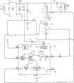
参照图4,本发明提出的原边控制的恒流开关电源控制器包括:Referring to Fig. 4, the constant current switching power supply controller of primary side control proposed by the present invention includes:
前沿消隐模块(LEB)100,所述的前沿消隐模块(LEB)100的输入端接电流采样端(CS),其输出端接比较器模块Uc(300)的正输入端,所述的前沿消隐模块(LEB)100用于对CS端的原边电流采样信号在开关电源的原边开关管开通瞬间产生的毛刺进行消隐,避免该毛刺对电路产生干扰;The leading edge blanking module (LEB) 100, the input terminal of the leading edge blanking module (LEB) 100 is connected to the current sampling terminal (CS), and its output terminal is connected to the positive input terminal of the comparator module Uc (300), the described The leading edge blanking module (LEB) 100 is used for blanking the glitch generated by the primary current sampling signal at the CS terminal when the primary switching tube of the switching power supply is turned on, so as to avoid the glitch from interfering with the circuit;
正弦半波基准产生模块200,所述的正弦半波基准产生模块200根据相位检测端(PD)检测到的反激变换器主电路输入整流桥的输出波形的相位,产生与其同频同相且幅值固定的正弦半波电压基准。Half sine wave
比较器模块300,所述的比较器模块300对经过前沿消隐模块(LEB)100后的原边电流采样波形和正弦半波基准产生模块200输出的正弦半波电压基准进行比较,当经过前沿消隐模块(LEB)100后的原边电流采样波形幅值上升触及到与正弦半波电压基准相同时,比较器模块300的输出电平由低电平置位到高电平,当经过前沿消隐模块(LEB)100后的原边电流采样波形幅值下降到小于正弦半波电压基准时,比较器模块的输出电平由高电平复位为低电平,比较器模块300包括比较器Uc。
采样保持模块400,所述的第二采样保持模块400对来自电压检测端(FB)的波形的高电平中间段进行采样保持,以获得比较准确的输出电压实时幅值,其中电压检测端直接或经电阻耦接到主电路变压器辅助绕组的一端。The sample and hold
电压/频率转换模块500,所述的电压/频率转换模块500一个输入端接采样保持模块400的输出,另一个输入端接频率设定端(FSET),所述的电压/频率转换模块500的输出为脉冲信号,脉冲信号的频率跟随采样保持模块400的输出信号电平幅值变化,当开关电源主电路的输出电压发生波动时,所述的电压/频率转换模块调节f/Vo使其为常数,其中Vo是开关电源主电路的输出电压,f是开关电源主电路工作频率。A voltage/
驱动脉冲产生模块600,所述的驱动脉冲产生模块600用于根据比较器模块300输出的信号和电压/频率转换模块500输出的脉冲信号来产生脉冲信号;驱动脉冲产生模块600可采用RS触发器实现,其中R脚接比较器模块300的输出,S脚接电压/频率转换模块500的输出:由当比较器模块300产生一个低电平到高电平的翻转时,驱动脉冲产生模块600的脉冲输出信号由高电平复位到低电平,即驱动脉冲产生模块输出主电路的原边开关管的关断触发信号从而使得开关电源的原边电流峰值包络线跟随所述的正弦半波电压基准;当电压/频率转换模块500输出的脉冲信号由低电平翻转为高电平时,即驱动脉冲产生模块输出主电路的原边开关管的导通触发信号,驱动脉冲产生模块600的脉冲输出信号由低电平置位到高电平;周而复始,产生脉冲序列控制开关电源的原边开关管;A driving pulse generating module 600, the driving pulse generating module 600 is used to generate a pulse signal according to the signal output by the comparator module 300 and the pulse signal output by the voltage/frequency conversion module 500; the driving pulse generating module 600 can use an RS flip-flop Implementation, wherein the R pin is connected to the output of the comparator module 300, and the S pin is connected to the output of the voltage/frequency conversion module 500: when the comparator module 300 generates a flip from low level to high level, the drive pulse generation module 600 The pulse output signal is reset from high level to low level, that is, the driving pulse generation module outputs the trigger signal for turning off the primary switch tube of the main circuit, so that the peak current envelope of the primary side current of the switching power supply follows the half-sine wave Voltage reference; when the pulse signal output by the voltage/frequency conversion module 500 is turned from low level to high level, that is, the drive pulse generation module outputs the conduction trigger signal of the primary switch tube of the main circuit, and the pulse of the drive pulse generation module 600 The output signal is set from low level to high level; it goes round and round to generate a pulse sequence to control the primary switching tube of the switching power supply;
驱动模块700,所述的驱动模块700的输入为驱动脉冲产生模块700的输出信号,用于增强所述驱动脉冲产生模块700的驱动能力。The
稳压模块800,所述的稳压模块800将外部接入的电源VDD转换成稳定的内部电源。The
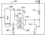
图5给出了正弦半波基准产生模块200的一个具体实施例:其中第一电阻201一端接相位检测端PD,第一电阻201另一端接三极管202的集电极、基极以及第一镜像电流源203和第二镜像电流源204的输入端,三极管202的发射极接地,第一镜像电流源203的输出接第二电阻205的一端、第一电容器206的一端以及除法器208的除数端(B),第二电阻205的另一端和第一电容器206的另一端接地,第二镜像电流源的另一端接第三电阻207的一端以及除法器208的被除数端,除法器208的输出端作为正弦半波基准产生模块200的输出端输出幅值恒定的正弦半波信号,其中三极管202也可以是金属氧化物半导体场效应管。Figure 5 shows a specific embodiment of the sine half-wave reference generation module 200: one end of the
图6(a)给出了采样保持电路400的一个具体实施例:Vcc可以是外接电源VDD或稳压模块800输出的直流电压;恒流源401一端接Vcc,另一端接第一开关402的一端,第一开关402的另一端与第二开关403的一端、第一电容器404的一端、第三开关405的一端和比较器408的正端相连,第二开关403的另一端与第一电容404的另一端相连之后接地,第三开关405的另一端、第二电容器406的一端、第四开关407的一端和比较器408的负端相连,第二电容406的另一端和第四开关407的另一端相连之后接地,比较器408的输出端与电阻409以及与门412的一个输入端相连,电阻409的另一端与第三电容器410的一端以及反相器411的输入端相连,反相器411的输出端与与门412的另一个输入端相连,与门412的输出端接第四开关407和第五开关414的门极和用来控制第四开关407和第五开关414的通断(高电平导通),第五开关414的一端接电压反馈端(FB),第五开关Sc5的另一端接第四电容器413的一端作为电压采样电路400的输出端,第四电容器Cc4的另一端接地;第一开关402、第二开关403、第三开关405的门极控制信号逻辑分别如图6(b)中Vgsc1、Vgsc2和Vgsc3波形所示,其中Vgsc1可由电压反馈端(FB)的高电平得到,Vgsc2由电压反馈端(FB)负电平区间中任意一段区间得到,Vgsc3由电压反馈端(FB)的负电平的前沿得到,本领域专业技术人员都可以通过现有技术实现产生上述三个逻辑电平信号;结合图6(b)波形对电压采样电路400的工作原理进行说明:VFB是电压反馈端(FB)的电压波形,V(A400)、V(B400)和V(C400)分别是图6(a)中A400、B400和C400各点波形,V400是采样保持电路400的输出波形;假设初始时VFB为正,第一开关402导通,恒流源Icc给第一电容器404线性充电;当VFB为零,第一开关402关断,第一电容器404的端电压V(A400)保持高电平,在VFB等于零或者小于零的区间里某个时间,第三开关405导通一小段区间,第一电容器404部分能量转移到第二电容器406,使第二电容器406的端电压V(B400)突变为高电平并保持;当VFB重新为正的时候,第二开关403导通一小段区间,将第一电容器404端电压V(A400)清零;第二开关403关断之后,第一开关402导通,恒流源Icc重新给第一电容器404线性充电;当第一电容器404端电压V(A400)上升的到大于第二电容器406的端电压V(B400)时,比较器408输出高电平;比较器4081输出的宽脉冲经电阻409、第三电容器410、反相器411和与门412构成的信号处理单元转换为窄脉冲Vgsamle,Vgsamle一方面接到第四开关407的门极,将第二电容406的端电压V(B400)进行清零,另一方面接到第五开关414的门极,对VFB的正电平进行采样;通过调节第一电容器404和第二电容器406的容值比,可以调整第二电容器406端电压V(B400)的高电平幅值,进而调整对VFB的正电平采样的时间点。Fig. 6 (a) has provided a specific embodiment of sample and hold circuit 400: Vcc can be the DC voltage that external power supply VDD or
其中,第一开关402、第二开关403、第三开关405、第四开关407和第五开关414可以是金属氧化物半导体场效应管,绝缘栅双极晶体管、双极晶体管或其它等效的开关电路构成。Wherein, the first switch 402, the second switch 403, the third switch 405, the fourth switch 407 and the fifth switch 414 may be metal oxide semiconductor field effect transistors, insulated gate bipolar transistors, bipolar transistors or other equivalent switch circuit configuration.
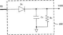
采样保持电路400也可以由图7所示二极管Dc、电容Cc和电阻Rc构成的简单的峰值采样保持电路实现,其中二极管Dc阳极接FB端,二极管阴极一端接电容Cc和电阻Rc的一端,电容Cc和电阻Rc的另一端接地;电阻Rc用来平衡Cc的电压,也可以用其它等效电路替代;图7所示的第二采样保持电路500优点是实现方式简单,缺点是对FB端正电平采样准确性较差。The sample-and-
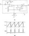
电压/频率转换模块500一个具体实施例如图8(a)所示,采样保持电路400的输出接第一二极管501的阳极,第一二极管501的阴极与第二二极管502的阴极相连,接到电阻503的一端,第二二极管502的阳极接电压源504,电阻503的另一端接电容器Ct的一端和开关506的一端后接到比较器508的正输入端,电容器Ct的另一端与开关506的一端接地,比较器508的负输入端接电源基准507(Vref),比较器508的输出接延时环节,延时环节的输出接开关506的控制端;图8(b)为图8(a)所示电压/频率转换模块500的主要工作波形,其中Vct为电容器Ct两端电压波形,V500为电压/频率转换模块500的输出波形,TD为延时环节的延时时间;采样保持电路400的输出电平V500远大于Vref,且电容器Ct取值较小,因此Vct的波形近似为三角波;在开关506关断区间,采样保持电路400的输出电压V400经电阻503给电容器Ct充电,当Vct电压上升到电压基准507(Vref),比较器508输出高电平,经延时环节后送到开关506的控制端,开关506导通,对电容器Ct放电,当Vct低于电压基准507(Vref),比较器508输出低电平,电容器Ct重新充电,延时环节的时间决定了电压/频率转换模块500输出的脉冲宽度;由于主电路启动瞬间V400电压为零,为了让主电路在启动时可以工作,电压源504经第二二极管502接到电阻503,从而可以使电路可以正常启动,并确定了电路的最低工作频率;V400电压越高,则电容Ct充电电流越大,频率越高,因此当FB输入正电平幅值发生变化时,电路的工作频率会相应变化;电容Ct经FSET端接到芯片外部,方便设置电路工作频率范围。A specific embodiment of the voltage/
电压/频率转换模块500也可采用压控振荡器电路来实现,如图9(a)所示的复位式压控振荡器电路,由第一电阻511、第二电阻514,电容Cx1,二极管512,电压源513、电流型运放515、开关516、电压源517(Vref2)以及比较器518组成,其中第一电阻511一端接采样保持电路400的输出端,第一电阻511的另一端与二极管512的阴极相连并接到运放515的负输入端,二极管512的阳极接电压源513的正极,电压源513的阴极接地,第二电阻514的一端接运放515的正输入端,第二电阻514的另一端接地,运放515的输出端接电容器Cx1、开关516的一端,并接到比较器518的正输入端,电容Cx1和开关516的另一端接地,比较器518的负输入端接电压源517(Vref2)的正极,电压源517(Vref2)的负极接地,比较器518的输出为电压/频率转换模块500的输出,并接开关516的控制端;图9(a)所示电路的主要波形如图9(b)所示,比较器518的输出脉冲的频率为:The voltage/frequency conversion module 500 can also be implemented by using a voltage-controlled oscillator circuit, such as the reset-type voltage-controlled oscillator circuit shown in Figure 9(a), consisting of a first resistor 511, a second resistor 514, a capacitor Cx1, and a diode 512 , a voltage source 513, a current-mode operational amplifier 515, a switch 516, a voltage source 517 (Vref2) and a comparator 518, wherein one end of the first resistor 511 is connected to the output end of the sample-and-hold circuit 400, and the other end of the first resistor 511 is connected to the diode The cathode of the diode 512 is connected and connected to the negative input terminal of the operational amplifier 515, the anode of the diode 512 is connected to the positive pole of the voltage source 513, the cathode of the voltage source 513 is grounded, one end of the second resistor 514 is connected to the positive input terminal of the operational amplifier 515, and the second The other end of resistor 514 is grounded, the output terminal of operational amplifier 515 is connected to capacitor Cx1, one end of switch 516, and connected to the positive input terminal of comparator 518, the other end of capacitor Cx1 and switch 516 is grounded, and the negative input terminal of comparator 518 Connect the positive pole of the voltage source 517 (Vref2), the negative pole of the voltage source 517 (Vref2) is grounded, the output of the comparator 518 is the output of the voltage/frequency conversion module 500, and connected to the control terminal of the switch 516; as shown in Figure 9 (a) The main waveform of the circuit is shown in Figure 9(b), and the frequency of the output pulse of the comparator 518 is:
其中,gm是电流型运放的跨导增益;由上式可以看到,当输入电压V500发生变化时,图9(a)所示电路频率可以跟随变化,改变Cx1也可以改变电路的频率,为了方便设置电路频率范围,将Cx1通过FSET端接到芯片外部;此外,为了让主电路可以正常启动,引入了箝位电压源513和二极管512,通过设定电压源517(Vref2)幅值可设定了电路的最低工作频率。Among them, gm is the transconductance gain of the current-mode operational amplifier; from the above formula, it can be seen that when the input voltage V500 changes, the frequency of the circuit shown in Figure 9(a) can follow the change, and changing Cx1 can also change the frequency of the circuit, In order to conveniently set the frequency range of the circuit, Cx1 is connected to the outside of the chip through FSET; in addition, in order to allow the main circuit to start normally, a clamping
进一步,作为本领域的专业技术人员也可选用其它现有的压控振荡器电路来实现所述电压/频率转换模块500的功能,如电荷平衡式压控振荡器等。Further, those skilled in the art may also select other existing voltage-controlled oscillator circuits to implement the functions of the voltage/
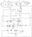
图10为本发明控制器000与反激式变换器主电路构成具有高功率因数隔离型原边恒流电路;交流输入电源10两端接整流桥11两个输入端,整流桥11的正输出端接第一电容器12(输入电容)的一端、第一电阻13、第二电阻23的一端、吸收网络16的一端和变压器17原边绕组的同名端,整流桥11的负输出端和第一电容器12的一端接地,第一电阻13的另一端接第二电容器14的一端、二极管15的一端和本发明控制器000供电端(VDD),第二电容器14的另一端接原边地,二极管15的另一端接变压器17辅助绕组的异名端和本发明控制器000电压反馈端(FB),第二电阻23的另一端接本发明控制器000的相位检测端(PD),变压器辅助绕组的同名端接地,吸收网络的一端接变压器17原边绕组的异名端和开关管18的漏极,开关管18的源极接第三电阻19(采样电阻)的一端和第四电阻22的一端,第四电阻22的另一端接本发明控制器000电流采样端(CS),开关管18的门极接本发明控制器000驱动端(DRV),第三电阻19的另一端接原边地,变压器17副边绕组的异名端接二极管20的阳极,二极管20的阴极接第三电容器21(输出电容)的正极,第三电容器21的负极接变压器17副边绕组的同名端,本发明控制器000接地端(GND)接原边地,本发明控制器频率设定(FSET)接电容第四电容器24的一端,第四电容器24的另一端接地;其中,整流桥11输出为正弦半波波形,第一电容器12为无极性小容量滤波电容,不影响整流桥11输出波形;吸收网络为电阻、电容和二极管构成的RCD吸收或其它吸收形式,开关管18可以是MOS管或三极管,第三电阻19用来对开关管电流进行采样,也可用其它等效电路替代;Figure 10 shows that the controller 000 of the present invention and the main circuit of the flyback converter form a high power factor isolated primary side constant current circuit; the two ends of the AC input power supply 10 are connected to the two input ends of the rectifier bridge 11, and the positive output of the rectifier bridge 11 Terminate one end of the first capacitor 12 (input capacitance), one end of the first resistor 13, one end of the second resistor 23, one end of the snubber network 16 and the same name end of the primary winding of the transformer 17, the negative output terminal of the rectifier bridge 11 and the first One end of the capacitor 12 is grounded, the other end of the first resistor 13 is connected to one end of the second capacitor 14, one end of the diode 15 and the power supply terminal (VDD) of the controller 000 of the present invention, the other end of the second capacitor 14 is connected to the primary ground, and the diode The other end of 15 is connected to the opposite end of the transformer 17 auxiliary winding and the voltage feedback terminal (FB) of the controller 000 of the present invention, and the other end of the second resistor 23 is connected to the phase detection terminal (PD) of the controller 000 of the present invention, and the auxiliary winding of the transformer The same-named end of the sink network is grounded, and one end of the absorption network is connected to the opposite-named end of the primary winding of the transformer 17 and the drain of the switch tube 18, and the source of the switch tube 18 is connected to one end of the third resistor 19 (sampling resistor) and one end of the fourth resistor 22 One end, the other end of the fourth resistor 22 is connected to the current sampling terminal (CS) of the controller 000 of the present invention, the gate of the switch tube 18 is connected to the drive terminal (DRV) of the controller 000 of the present invention, and the other end of the third resistor 19 is connected to the primary side Ground, the anode of the diode 20 connected to the opposite end of the secondary winding of the transformer 17, the cathode of the diode 20 connected to the positive pole of the third capacitor 21 (output capacitor), and the negative pole of the third capacitor 21 connected to the terminal of the same name of the secondary winding of the transformer 17. The ground terminal (GND) of the
图11为图10所示电路的主要波形,其中,v200是正弦半波基准产生模块200的输出波形,v300是比较器模块300的输出波形,v400是锯齿波产生模块400的输出波形,v500是电压/频率转换模块500的输出波形,vDRV是驱动模块700的输出波形,ipri是原边开关管18的电流波形,isec是副边二极管20的电流波形。Fig. 11 is the main waveform of the circuit shown in Fig. 10, wherein, v200 is the output waveform of the half-sine wave
本发明可以应用到隔离型输出,也可以应用到非隔离型输出。图12为本发明控制器000与一种非隔离的升降压(buck-boost)电路的主电路连接示意图。其中,非隔离的升降压(buck-boost)电路包括输入交流电源10、输入整流桥11、第一电容器12、第一电阻13、、第二电容器14、第一二极管15、电感17、开关管18、第二电阻19、第二二极管20、第三电容器21、第三电阻22、第四电阻23、第四电容器24和本发明控制器000;其中,输入整流桥11的两个输入端分别接输入交流电源10的两端,输入整流桥11的正输出端接第一电容器12的一端、第一电阻13的一端、电感17主绕组的同名端、第二二极管20的阴极和第四电阻23的一端,第一电阻13的一端接第二电容器14的一端、第一二极管15的一端和控制器000的供电端(VDD),第四电阻23的另一端接控制器000的相位检测端(PD),第一二极管15的阳极接电感17的耦合绕组的异名端以及控制器000的电压反馈端(FB),电感17的耦合绕组的同名端接地,电感17的耦合绕组的异名端电感17的异名端接开关管18的漏极以及第三电容器21的正极,第三电容器21的负极接第二二极管20的阳极,开关管18的源极接第二电阻19的一端以及第三电阻22的一端,第二电阻19的另一端接地,第三电阻22的另一端接控制器000的电流采样端(CS),开关管18的源极的门极接控制器000的驱动端(DRV),控制器000的频率设定段(PSET)接第四电容器24的一端,第四电容器24的另一端接地。The present invention can be applied to isolated output, and can also be applied to non-isolated output. FIG. 12 is a schematic diagram of the main circuit connection between the
本发明包括的具体模块如前沿消隐模块100、正弦半波基准产生模块200、采样保持模块400、电压/频率转换模块500等,本领域技术人员可以在不违背其精神的前提下,可以有多种实施方式,或通过各种不同的组合方式,形成不同的具体实施例,这里不再详细描述。The specific modules included in the present invention are such as leading
无论上文说明如何详细,还有可以有许多方式实施本发明,说明书中所述的只是本发明的一个具体实施例子。凡根据本发明精神实质所做的等效变换或修饰,都应涵盖在本发明的保护范围之内。No matter how detailed the above description is, there are still many ways to implement the present invention, and what is described in the specification is only a specific implementation example of the present invention. All equivalent changes or modifications made according to the spirit of the present invention shall fall within the protection scope of the present invention.
本发明实施例的上述详细说明并不是穷举的或者用于将本发明限制在上述明确的形式上。在上述以示意性目的说明本发明的特定实施例和实例的同时,本领域技术人员将认识到可以在本发明的范围内进行各种等同修改。The above detailed description of embodiments of the invention is not intended to be exhaustive or to limit the invention to the precise forms described above. While specific embodiments of, and examples for, the invention were described above for illustrative purposes, various equivalent modifications are possible within the scope of the invention, those skilled in the relevant art will recognize.
在上述说明描述了本发明的特定实施例并且描述了预期最佳模式的同时,无论在上文中出现了如何详细的说明,也可以许多方式实施本发明。上述电路结构及其控制方式的细节在其执行细节中可以进行相当多的变化,然而其仍然包含在这里所公开的本发明中。While the above description describes particular embodiments of the invention and describes the best mode contemplated, no matter how detailed the foregoing description appears, the invention can be practiced in many ways. The details of the above-described circuit structure and its control manner may vary considerably in its implementation details, yet it is still included in the invention disclosed herein.
如上述一样应当注意,在说明本发明的某些特征或者方案时所使用的特殊术语不应当用于表示在这里重新定义该术语以限制与该术语相关的本发明的某些特定特点、特征或者方案。总之,不应当将在随附的权利要求书中使用的术语解释为将本发明限定在说明书中公开的特定实施例,除非上述详细说明部分明确地限定了这些术语。因此,本发明的实际范围不仅包括所公开的实施例,还包括在权利要求书之下实施或者执行本发明的所有等效方案。As above, it should be noted that specific terms used in describing certain features or solutions of the present invention should not be used to indicate that the terms are redefined here to limit some specific features, features or aspects of the present invention to which the terms are related. plan. In conclusion, the terms used in the following claims should not be construed to limit the invention to the particular embodiments disclosed in the specification, unless the above detailed description expressly defines those terms. Accordingly, the actual scope of the invention includes not only the disclosed embodiments, but also all equivalent arrangements which practice or perform the invention under the claims.
Claims (10)
Translated fromChinesePriority Applications (1)
| Application Number | Priority Date | Filing Date | Title |
|---|---|---|---|
| CN2011100345342ACN102364857B (en) | 2011-02-01 | 2011-02-01 | Primary side constant current switching power controller and method |
Applications Claiming Priority (1)
| Application Number | Priority Date | Filing Date | Title |
|---|---|---|---|
| CN2011100345342ACN102364857B (en) | 2011-02-01 | 2011-02-01 | Primary side constant current switching power controller and method |
Publications (2)
| Publication Number | Publication Date |
|---|---|
| CN102364857A CN102364857A (en) | 2012-02-29 |
| CN102364857Btrue CN102364857B (en) | 2012-12-12 |
Family
ID=45691411
Family Applications (1)
| Application Number | Title | Priority Date | Filing Date |
|---|---|---|---|
| CN2011100345342AExpired - Fee RelatedCN102364857B (en) | 2011-02-01 | 2011-02-01 | Primary side constant current switching power controller and method |
Country Status (1)
| Country | Link |
|---|---|
| CN (1) | CN102364857B (en) |
Families Citing this family (24)
| Publication number | Priority date | Publication date | Assignee | Title |
|---|---|---|---|---|
| CN102684517B (en)* | 2012-05-24 | 2014-08-06 | 深圳市明微电子股份有限公司 | Switch power supply with high power factor and controller of switch power supply |
| CN102751696B (en)* | 2012-06-28 | 2013-06-19 | 天津大学 | Chip over-current protection circuit with adjustable delay time |
| CN103812323A (en)* | 2012-11-08 | 2014-05-21 | 常州隆辉照明科技有限公司 | Power factor compensating circuit |
| CN103424601B (en)* | 2013-08-21 | 2015-08-19 | 矽力杰半导体技术(杭州)有限公司 | A kind of voltage detecting circuit |
| CN104753605A (en)* | 2013-12-27 | 2015-07-01 | 华为技术有限公司 | Optical line terminal |
| CN104640326B (en)* | 2015-02-25 | 2017-03-29 | 苏州智浦芯联电子科技股份有限公司 | The high precision constant current LED drive circuit realized using digital method |
| CN105120571B (en) | 2015-09-14 | 2018-05-01 | 昂宝电子(上海)有限公司 | Systems and methods for current regulation in light emitting diode lighting systems |
| CN105490532B (en)* | 2016-01-06 | 2019-04-12 | 深圳欧创芯半导体有限公司 | DC-DC converter and system |
| CN107027201B (en)* | 2016-02-02 | 2020-10-30 | 佛山市顺德区美的电热电器制造有限公司 | Electromagnetic heating device and noise reduction control method thereof |
| CN106300925B (en)* | 2016-08-26 | 2018-07-17 | 杰华特微电子(杭州)有限公司 | Drive control circuit, method and its system of AC-DC circuits |
| CN106255270B (en)* | 2016-08-30 | 2019-02-22 | 华中科技大学 | Primary-side feedback flyback LED constant current driver based on power tube drain detection technology |
| CN106535409A (en)* | 2016-12-03 | 2017-03-22 | 河池学院 | Constant current switching power supply system for LED illumination |
| CN107817376B (en)* | 2017-11-15 | 2023-09-05 | 武汉合智数字能源技术有限公司 | A Negative Half Cycle Waveform Blanking Amplitude Sampling Device |
| CN108303579B (en)* | 2018-01-26 | 2020-08-25 | 成都芯源系统有限公司 | Voltage detection circuit and method |
| CN108736706B (en)* | 2018-08-01 | 2024-07-19 | 杭州老板电器股份有限公司 | Controllable switch power supply and purifying water tank comprising same |
| CN109168226A (en)* | 2018-10-25 | 2019-01-08 | 英飞特电子(杭州)股份有限公司 | A kind of LED adjusting method and circuit |
| CN109245546B (en)* | 2018-10-30 | 2020-07-03 | 西安微电子技术研究所 | Sampling compensation circuit and primary side feedback flyback converter |
| CN111163565B (en)* | 2020-02-25 | 2025-04-29 | 深圳市晟碟半导体有限公司 | A LED driving circuit and driving method for reducing harmonic distortion |
| CN111682773B (en)* | 2020-05-14 | 2021-09-21 | 杭州电子科技大学 | Primary side constant current controlled resonance conversion device and implementation method |
| CN111711364B (en)* | 2020-06-24 | 2023-03-21 | 电子科技大学 | Self-adaptive leading edge blanking circuit based on high-precision load current detection technology |
| CN112466110B (en)* | 2020-10-29 | 2024-02-23 | 欧普照明电器(中山)有限公司 | Equipment control system and equipment control method |
| CN113300587B (en)* | 2021-05-18 | 2022-07-15 | 西南交通大学 | A pulse sequence control method and device for a power factor correction converter |
| CN114244116B (en)* | 2021-12-21 | 2023-09-05 | 中国电子科技集团公司第二十四研究所 | Mode discrimination circuit for BUCK-BOOST controller |
| CN116131219B (en)* | 2023-02-16 | 2023-06-30 | 恩赛半导体(成都)有限公司 | Overvoltage protection circuit and electronic device |
Family Cites Families (4)
| Publication number | Priority date | Publication date | Assignee | Title |
|---|---|---|---|---|
| US7317625B2 (en)* | 2004-06-04 | 2008-01-08 | Iwatt Inc. | Parallel current mode control using a direct duty cycle algorithm with low computational requirements to perform power factor correction |
| US7554473B2 (en)* | 2007-05-02 | 2009-06-30 | Cirrus Logic, Inc. | Control system using a nonlinear delta-sigma modulator with nonlinear process modeling |
| US8279631B2 (en)* | 2008-08-05 | 2012-10-02 | Active-Semi, Inc. | Limiting primary peak charge to control output current of a flyback converter |
| CN101951177B (en)* | 2010-09-06 | 2014-05-07 | Bcd半导体制造有限公司 | Switching power supply system and switching power supply control circuit |
- 2011
- 2011-02-01CNCN2011100345342Apatent/CN102364857B/ennot_activeExpired - Fee Related
Also Published As
| Publication number | Publication date |
|---|---|
| CN102364857A (en) | 2012-02-29 |
Similar Documents
| Publication | Publication Date | Title |
|---|---|---|
| CN102364857B (en) | Primary side constant current switching power controller and method | |
| CN102368662B (en) | Current reference generating circuit, control circuit and method of constant current switching power supply | |
| CN102364848A (en) | A primary-side controlled constant current switching power supply controller and method | |
| US10291141B1 (en) | Flyback converter | |
| US9054592B2 (en) | Synchronous rectifying control method and circuit for isolated switching power supply | |
| US8988901B2 (en) | Switching power supply device | |
| US8625319B2 (en) | Bridgeless PFC circuit for critical continuous current mode and controlling method thereof | |
| US8456868B2 (en) | Controller for a resonant switched-mode power converter | |
| CN113937988B (en) | Asymmetric half-bridge flyback converter and control method thereof | |
| CN102364858B (en) | Constant-current switching power supply controller capable of controlling through primary side and method | |
| US20090230929A1 (en) | Bridgeless pfc circuit for crm and controlling method thereof | |
| KR100829121B1 (en) | Power Factor Correction Circuit for Single Power Operation in BCM Mode | |
| CN113300606B (en) | Flyback converter and control method thereof | |
| US10523127B1 (en) | Output clamped flyback converter | |
| CN108418435B (en) | Synchronous rectification flyback DC-DC power supply conversion device | |
| CN104660028B (en) | A kind of circuit of power factor correction | |
| Lee et al. | Soft-switching two-switch resonant AC–DC converter with high power factor | |
| CN103490636A (en) | Quasi-resonant control method, quasi-resonant system and quasi-resonant device for switching power supplies | |
| CN103298215B (en) | Control circuit of flyback LED (Light Emitting Diode) driver | |
| CN102208870B (en) | Method and apparatus for detecting continuous current mode operation of a magnetic device | |
| CN106255270A (en) | Primary side feedback inverse-excitation type LED constant-current driver based on power tube drain electrode detection technique | |
| CN110829846A (en) | A zero-voltage switching control circuit and method applied to switching power supply | |
| CN110943624A (en) | A zero-voltage switching resonant power conversion circuit and converter | |
| US11637489B2 (en) | Isolated DC/DC converter and AC/DC converter | |
| CN203206143U (en) | Step-down switching power supply |
Legal Events
| Date | Code | Title | Description |
|---|---|---|---|
| C06 | Publication | ||
| PB01 | Publication | ||
| C10 | Entry into substantive examination | ||
| SE01 | Entry into force of request for substantive examination | ||
| C14 | Grant of patent or utility model | ||
| GR01 | Patent grant | ||
| CF01 | Termination of patent right due to non-payment of annual fee | ||
| CF01 | Termination of patent right due to non-payment of annual fee | Granted publication date:20121212 |