CN102362551A - organic electroluminescent element - Google Patents
organic electroluminescent elementDownload PDFInfo
- Publication number
- CN102362551A CN102362551ACN2010800125863ACN201080012586ACN102362551ACN 102362551 ACN102362551 ACN 102362551ACN 2010800125863 ACN2010800125863 ACN 2010800125863ACN 201080012586 ACN201080012586 ACN 201080012586ACN 102362551 ACN102362551 ACN 102362551A
- Authority
- CN
- China
- Prior art keywords
- layer
- organic
- light
- carbon number
- general formula
- Prior art date
- Legal status (The legal status is an assumption and is not a legal conclusion. Google has not performed a legal analysis and makes no representation as to the accuracy of the status listed.)
- Granted
Links
- 0CCC1(c(cccc2)*2NC=C(CCC2CC2)C=NC11C)I1#CChemical compoundCCC1(c(cccc2)*2NC=C(CCC2CC2)C=NC11C)I1#C0.000description8
- IDQAKRKCZPTEHT-UHFFFAOYSA-OC(Cc(c1ccccc11)c[n]1-c1nccc[nH+]1)c(c1ccccc11)c[n]1-c1ncncn1Chemical compoundC(Cc(c1ccccc11)c[n]1-c1nccc[nH+]1)c(c1ccccc11)c[n]1-c1ncncn1IDQAKRKCZPTEHT-UHFFFAOYSA-O0.000description1
- XIULBLKYTAHTOK-SFHVURJKSA-NC(Cc1ncncn1)[C@@H]1c2ccccc2-c2ccc(c3ccccc3[n]3-c4ncncn4)c3c2C1Chemical compoundC(Cc1ncncn1)[C@@H]1c2ccccc2-c2ccc(c3ccccc3[n]3-c4ncncn4)c3c2C1XIULBLKYTAHTOK-SFHVURJKSA-N0.000description1
- HVZRQKHGGRUAOX-CRBKLXRCSA-NC/C=C\c1c(C[n]2c(c3c(cc4)c5ccccc5[n]3-c3ccccc3)c4c3ccccc23)cccc1C[n]1c(cccc2)c2c(C=C[C@@H]2c3c4cccc3)c1C2N4c1ccccc1Chemical compoundC/C=C\c1c(C[n]2c(c3c(cc4)c5ccccc5[n]3-c3ccccc3)c4c3ccccc23)cccc1C[n]1c(cccc2)c2c(C=C[C@@H]2c3c4cccc3)c1C2N4c1ccccc1HVZRQKHGGRUAOX-CRBKLXRCSA-N0.000description1
- QYOZUCWQTIMJJV-RSWYKCFKSA-NCC(NC/N=C\N)N(c1ccccc1/C1=C/C2C)/C1=C/Cc(cccc1)c1N2c1ncccn1Chemical compoundCC(NC/N=C\N)N(c1ccccc1/C1=C/C2C)/C1=C/Cc(cccc1)c1N2c1ncccn1QYOZUCWQTIMJJV-RSWYKCFKSA-N0.000description1
- RNZIXAPSKQTUQE-FQEVSTJZSA-NC[C@@H](c1ncccc1)[I]1c(cc(c(cccc2)c2[N-]2-c3ncccc3)c2c2)c2-c2ccccc12Chemical compoundC[C@@H](c1ncccc1)[I]1c(cc(c(cccc2)c2[N-]2-c3ncccc3)c2c2)c2-c2ccccc12RNZIXAPSKQTUQE-FQEVSTJZSA-N0.000description1
- CXDHSSOKAXIQSG-DAHUVGKNSA-NC[C@H](/C=C\C=C)c1cc(ccc(c2c3cccc2)c2[n]3-c3ccccc3)c2[n]1-c1cccc(-[n]2c(-c3c(CC4)c(cccc5)c5[n]3-c3ccccc3)c4c3ccccc23)n1Chemical compoundC[C@H](/C=C\C=C)c1cc(ccc(c2c3cccc2)c2[n]3-c3ccccc3)c2[n]1-c1cccc(-[n]2c(-c3c(CC4)c(cccc5)c5[n]3-c3ccccc3)c4c3ccccc23)n1CXDHSSOKAXIQSG-DAHUVGKNSA-N0.000description1
- ARHYSXKRLZTEAO-UHFFFAOYSA-Nc(cc1)cc(c2ccc(c3ccccc3[n]3-c4ncncc4)c3c22)c1[n]2-c1ccccn1Chemical compoundc(cc1)cc(c2ccc(c3ccccc3[n]3-c4ncncc4)c3c22)c1[n]2-c1ccccn1ARHYSXKRLZTEAO-UHFFFAOYSA-N0.000description1
- MZYDBGLUVPLRKR-UHFFFAOYSA-Nc(cc1)cc(c2ccccc22)c1[n]2-c1cc(-[n]2c3ccccc3c3c2cccc3)ccc1Chemical compoundc(cc1)cc(c2ccccc22)c1[n]2-c1cc(-[n]2c3ccccc3c3c2cccc3)ccc1MZYDBGLUVPLRKR-UHFFFAOYSA-N0.000description1
- KWMIIWDUQBSERL-UHFFFAOYSA-Nc(cc1)ccc1-[n]1c2cc(c3ccccc3[n]3-c4ccccc4)c3nc2c2ccccc12Chemical compoundc(cc1)ccc1-[n]1c2cc(c3ccccc3[n]3-c4ccccc4)c3nc2c2ccccc12KWMIIWDUQBSERL-UHFFFAOYSA-N0.000description1
- OFELAVAVZOCYSS-UHFFFAOYSA-Nc(cc1)ccc1-c1nc(-[n]2c3ccccc3c3c2cccc3)nc(-[n](c(cccc2)c2c2ccc3c4c5cccc4)c2c3[n]5-c2ccccc2)n1Chemical compoundc(cc1)ccc1-c1nc(-[n]2c3ccccc3c3c2cccc3)nc(-[n](c(cccc2)c2c2ccc3c4c5cccc4)c2c3[n]5-c2ccccc2)n1OFELAVAVZOCYSS-UHFFFAOYSA-N0.000description1
Images

Classifications
- C—CHEMISTRY; METALLURGY
- C09—DYES; PAINTS; POLISHES; NATURAL RESINS; ADHESIVES; COMPOSITIONS NOT OTHERWISE PROVIDED FOR; APPLICATIONS OF MATERIALS NOT OTHERWISE PROVIDED FOR
- C09K—MATERIALS FOR MISCELLANEOUS APPLICATIONS, NOT PROVIDED FOR ELSEWHERE
- C09K11/00—Luminescent, e.g. electroluminescent, chemiluminescent materials
- C09K11/06—Luminescent, e.g. electroluminescent, chemiluminescent materials containing organic luminescent materials
- H—ELECTRICITY
- H05—ELECTRIC TECHNIQUES NOT OTHERWISE PROVIDED FOR
- H05B—ELECTRIC HEATING; ELECTRIC LIGHT SOURCES NOT OTHERWISE PROVIDED FOR; CIRCUIT ARRANGEMENTS FOR ELECTRIC LIGHT SOURCES, IN GENERAL
- H05B33/00—Electroluminescent light sources
- H05B33/12—Light sources with substantially two-dimensional radiating surfaces
- H05B33/22—Light sources with substantially two-dimensional radiating surfaces characterised by the chemical or physical composition or the arrangement of auxiliary dielectric or reflective layers
- H—ELECTRICITY
- H10—SEMICONDUCTOR DEVICES; ELECTRIC SOLID-STATE DEVICES NOT OTHERWISE PROVIDED FOR
- H10K—ORGANIC ELECTRIC SOLID-STATE DEVICES
- H10K50/00—Organic light-emitting devices
- H10K50/10—OLEDs or polymer light-emitting diodes [PLED]
- H10K50/11—OLEDs or polymer light-emitting diodes [PLED] characterised by the electroluminescent [EL] layers
- H—ELECTRICITY
- H10—SEMICONDUCTOR DEVICES; ELECTRIC SOLID-STATE DEVICES NOT OTHERWISE PROVIDED FOR
- H10K—ORGANIC ELECTRIC SOLID-STATE DEVICES
- H10K50/00—Organic light-emitting devices
- H10K50/10—OLEDs or polymer light-emitting diodes [PLED]
- H10K50/18—Carrier blocking layers
- H—ELECTRICITY
- H10—SEMICONDUCTOR DEVICES; ELECTRIC SOLID-STATE DEVICES NOT OTHERWISE PROVIDED FOR
- H10K—ORGANIC ELECTRIC SOLID-STATE DEVICES
- H10K50/00—Organic light-emitting devices
- H10K50/10—OLEDs or polymer light-emitting diodes [PLED]
- H10K50/18—Carrier blocking layers
- H10K50/181—Electron blocking layers
- H—ELECTRICITY
- H10—SEMICONDUCTOR DEVICES; ELECTRIC SOLID-STATE DEVICES NOT OTHERWISE PROVIDED FOR
- H10K—ORGANIC ELECTRIC SOLID-STATE DEVICES
- H10K85/00—Organic materials used in the body or electrodes of devices covered by this subclass
- H10K85/30—Coordination compounds
- H10K85/321—Metal complexes comprising a group IIIA element, e.g. Tris (8-hydroxyquinoline) gallium [Gaq3]
- H10K85/324—Metal complexes comprising a group IIIA element, e.g. Tris (8-hydroxyquinoline) gallium [Gaq3] comprising aluminium, e.g. Alq3
- H—ELECTRICITY
- H10—SEMICONDUCTOR DEVICES; ELECTRIC SOLID-STATE DEVICES NOT OTHERWISE PROVIDED FOR
- H10K—ORGANIC ELECTRIC SOLID-STATE DEVICES
- H10K85/00—Organic materials used in the body or electrodes of devices covered by this subclass
- H10K85/30—Coordination compounds
- H10K85/341—Transition metal complexes, e.g. Ru(II)polypyridine complexes
- H10K85/342—Transition metal complexes, e.g. Ru(II)polypyridine complexes comprising iridium
- H—ELECTRICITY
- H10—SEMICONDUCTOR DEVICES; ELECTRIC SOLID-STATE DEVICES NOT OTHERWISE PROVIDED FOR
- H10K—ORGANIC ELECTRIC SOLID-STATE DEVICES
- H10K85/00—Organic materials used in the body or electrodes of devices covered by this subclass
- H10K85/60—Organic compounds having low molecular weight
- H10K85/649—Aromatic compounds comprising a hetero atom
- H10K85/654—Aromatic compounds comprising a hetero atom comprising only nitrogen as heteroatom
- H—ELECTRICITY
- H10—SEMICONDUCTOR DEVICES; ELECTRIC SOLID-STATE DEVICES NOT OTHERWISE PROVIDED FOR
- H10K—ORGANIC ELECTRIC SOLID-STATE DEVICES
- H10K85/00—Organic materials used in the body or electrodes of devices covered by this subclass
- H10K85/60—Organic compounds having low molecular weight
- H10K85/649—Aromatic compounds comprising a hetero atom
- H10K85/657—Polycyclic condensed heteroaromatic hydrocarbons
- H10K85/6572—Polycyclic condensed heteroaromatic hydrocarbons comprising only nitrogen in the heteroaromatic polycondensed ring system, e.g. phenanthroline or carbazole
- C—CHEMISTRY; METALLURGY
- C09—DYES; PAINTS; POLISHES; NATURAL RESINS; ADHESIVES; COMPOSITIONS NOT OTHERWISE PROVIDED FOR; APPLICATIONS OF MATERIALS NOT OTHERWISE PROVIDED FOR
- C09K—MATERIALS FOR MISCELLANEOUS APPLICATIONS, NOT PROVIDED FOR ELSEWHERE
- C09K2211/00—Chemical nature of organic luminescent or tenebrescent compounds
- C09K2211/10—Non-macromolecular compounds
- C09K2211/1018—Heterocyclic compounds
- C09K2211/1025—Heterocyclic compounds characterised by ligands
- C09K2211/1029—Heterocyclic compounds characterised by ligands containing one nitrogen atom as the heteroatom
- H—ELECTRICITY
- H10—SEMICONDUCTOR DEVICES; ELECTRIC SOLID-STATE DEVICES NOT OTHERWISE PROVIDED FOR
- H10K—ORGANIC ELECTRIC SOLID-STATE DEVICES
- H10K2101/00—Properties of the organic materials covered by group H10K85/00
- H10K2101/10—Triplet emission
- H—ELECTRICITY
- H10—SEMICONDUCTOR DEVICES; ELECTRIC SOLID-STATE DEVICES NOT OTHERWISE PROVIDED FOR
- H10K—ORGANIC ELECTRIC SOLID-STATE DEVICES
- H10K2101/00—Properties of the organic materials covered by group H10K85/00
- H10K2101/30—Highest occupied molecular orbital [HOMO], lowest unoccupied molecular orbital [LUMO] or Fermi energy values
Landscapes
- Chemical & Material Sciences (AREA)
- Engineering & Computer Science (AREA)
- Materials Engineering (AREA)
- Physics & Mathematics (AREA)
- Optics & Photonics (AREA)
- Spectroscopy & Molecular Physics (AREA)
- Organic Chemistry (AREA)
- Inorganic Chemistry (AREA)
- Crystallography & Structural Chemistry (AREA)
- Electroluminescent Light Sources (AREA)
- Nitrogen Condensed Heterocyclic Rings (AREA)
Abstract
Description
Translated fromChinese技术领域technical field
本发明涉及含有吲哚并咔唑化合物的有机电致发光元件,详细而言,涉及对由有机化合物构成的发光层施加电场而放出光的薄膜型器件。The present invention relates to an organic electroluminescent device containing an indolocarbazole compound, and more specifically, to a thin-film device that emits light by applying an electric field to a light-emitting layer made of an organic compound.
背景技术Background technique
一般而言,有机电致发光元件(以下,称为有机EL元件),作为其最简单的结构由夹着发光层的一对对置电极构成。即,在有机EL元件中,利用如下现象:当在两电极间施加电场时,从阴极注入电子,从阳极注入空穴,它们在发光层中复合,放出光。In general, an organic electroluminescence element (hereinafter, referred to as an organic EL element) is constituted by a pair of opposing electrodes sandwiching a light-emitting layer as its simplest structure. That is, in an organic EL element, a phenomenon is utilized in which electrons are injected from the cathode and holes are injected from the anode when an electric field is applied between the two electrodes, and these recombine in the light-emitting layer to emit light.
近年来,进行了使用有机薄膜的有机EL元件的开发。特别是为了提高发光效率,以从电极的载流子的注入提高为目的,对电极的种类进行了最优化,开发了在电极间将包含芳香族二胺的空穴传输层和包含8-羟基喹啉铝络合物(Alq3)的发光层作为薄膜而设置的元件,由此与以往的使用了蒽等的单晶的元件相比,进行了大幅的发光效率的改善,因此,以面向具有自发光·高速应答性这样的特征的高性能平板的实用化的目标进行了发展。In recent years, development of organic EL elements using organic thin films has been advanced. In particular, in order to improve the luminous efficiency and improve the injection of carriers from the electrodes, the type of electrodes was optimized, and a hole transport layer containing aromatic diamine and a layer containing 8-hydroxyl were developed between the electrodes. The device in which the light-emitting layer of quinoline aluminum complex (Alq3) is provided as a thin film has greatly improved the luminous efficiency compared with the conventional device using a single crystal such as anthracene. The goal is to realize the practical application of high-performance flat panels with characteristics such as self-illumination and high-speed response.
另外,作为提高元件的发光效率的尝试,还在研究不使用荧光而使用磷光。以上述的设置了包含芳香族二胺的空穴传输层和包含Alq3的发光层的元件为首的许多元件利用荧光发光而成,但通过使用磷光发光、即利用来自三重激发态的发光,与以往的使用荧光(单重态)的元件相比,可期待提高3~4倍左右的效率提高。为了该目的,对将香豆素衍生物、二苯甲酮衍生物作为发光层进行了研究,但只得到极低的亮度。另外,作为利用三重态的尝试,对使用铕络合物进行了研究,但这也未达到高效率的发光。近年来,如专利文献1中举出的那样以发光的高效率化、长寿命化为目的,以铱络合物等的有机金属络合物为中心进行了许多研究。In addition, as an attempt to improve the luminous efficiency of the device, the use of phosphorescence instead of fluorescence has been studied. Many devices, including the above-mentioned device provided with a hole transport layer containing aromatic diamine and a light emitting layer containing Alq3, are produced by fluorescence emission, but by using phosphorescence emission, that is, emission from a triplet excited state, it is different from conventional Compared with conventional devices using fluorescence (singlet state), an efficiency improvement of about 3 to 4 times can be expected. For this purpose, coumarin derivatives and benzophenone derivatives have been studied as light-emitting layers, but only extremely low luminance was obtained. In addition, as an attempt to utilize the triplet state, the use of europium complexes has been studied, but high-efficiency light emission has not yet been achieved. In recent years, as mentioned in
现有技术文献prior art literature
专利文献patent documents
专利文献1:特表2003-515897号公报Patent Document 1: Special Publication No. 2003-515897
专利文献2:特开平11-162650号公报Patent Document 2: Japanese Unexamined Patent Application Publication No. H11-162650
专利文献3:特平11-176578号公报Patent Document 3: Japanese Patent Publication No. 11-176578
非专利文献non-patent literature
非专利文献1:New Journal of Chemistry 2002,26,1171Non-Patent Document 1: New Journal of Chemistry 2002, 26, 1171
非专利文献2:APPLIED PHYSICS LETTERS 2003,83,3818Non-Patent Document 2: APPLIED PHYSICS LETTERS 2003, 83, 3818
非专利文献3:APPLIED PHYSICS LETTERS 2003,93,143307Non-Patent Document 3: APPLIED PHYSICS LETTERS 2003, 93, 143307
但是,有机EL元件,通过从两电极平衡良好地向发光层注入空穴及电子、注入的空穴及电子在发光层中有效地复合,由此得到良好的发光效率。换句话说,由于两电荷向发光层中注入平衡、在发光层内的两电荷的传输平衡破坏,因此产生电荷向传输层的泄露,在发光层内的复合概率降低。进而在两电荷的平衡破坏了的状态下,发光层内的复合区域被限定在传输层界面附近的狭小区域。在这种情况下,产生激子从发光层向传输层的泄露,导致发光效率的降低。特别是电子以及激子向空穴传输层的泄露,在招致发光效率的降低的同时招致起因于空穴传输材料的劣化的元件寿命降低,因此,成为极其重要的问题。However, in an organic EL element, holes and electrons are well-balancedly injected from both electrodes into the light-emitting layer, and the injected holes and electrons are efficiently recombined in the light-emitting layer, whereby good luminous efficiency is obtained. In other words, since the balance of the injection of the two charges into the light-emitting layer breaks the transfer balance of the two charges in the light-emitting layer, leakage of charges to the transport layer occurs, and the probability of recombination in the light-emitting layer decreases. Furthermore, in the state where the balance of the two electric charges is broken, the recombination region in the light-emitting layer is limited to a narrow region near the interface of the transport layer. In this case, leakage of excitons from the light-emitting layer to the transport layer occurs, resulting in a decrease in luminous efficiency. In particular, leakage of electrons and excitons to the hole transport layer causes a decrease in luminous efficiency and a decrease in device life due to degradation of the hole transport material, and thus becomes an extremely important problem.
为了解决上述的问题,在非专利文献1中提案有使用下述化合物在发光层的阳极侧界面设置电子及/或激子阻挡层,在效率提高方面提高效果。In order to solve the above-mentioned problems, Non-Patent
进而,在非专利文献2、3中公开有使用1,3-二咔唑基苯(mCP)作为电子阻挡层、激子阻挡层的例子。Furthermore,

但是,在这些元件中,由于驱动电压高、另外使用的化合物的耐久性不足,因此具有不能显示出实用的发光特性和驱动寿命的课题。However, in these devices, since the driving voltage is high and the durability of the separately used compound is insufficient, there is a problem that practical light emitting characteristics and driving life cannot be exhibited.
即,作为用于实现显示出良好的发光特性和寿命特性的有机EL元件的方法,有通过在空穴传输层与发光层之间插入有机层、由此阻止电子及/或激子向空穴传输层泄露的手法,但发挥该功能的实用水平的材料处于未知的状况。在空穴传输层和发光层之间插入的有机层,由于为阻止电子及/或激子向空穴传输层泄露的有机层,因此也称为电子阻挡层或激子阻挡层。本发明书中所谓的电子及/或激子阻挡层是指该有机层。以下,也将电子及/或激子阻挡层称为EB层。That is, as a method for realizing an organic EL device exhibiting good light emission characteristics and life characteristics, there is an organic layer inserted between the hole transport layer and the light emission layer, thereby preventing the transfer of electrons and/or excitons to holes. The means by which the transport layer is leaked, but materials at a practical level to perform this function are unknown. The organic layer interposed between the hole transport layer and the light emitting layer is also called an electron blocking layer or an exciton blocking layer because it prevents leakage of electrons and/or excitons to the hole transport layer. The term "electron and/or exciton blocking layer" in this specification refers to this organic layer. Hereinafter, the electron and/or exciton blocking layer is also referred to as an EB layer.
另一方面,专利文献2以及专利文献3公开了以下的吲哚并咔唑化合物,虽然这些专利文献公开了含有吲哚并咔唑化合物作为电荷传输成分,推荐作为空穴注入层或空穴传输层的材料使用,但没有教导作为在发光层和空穴传输层之间与发光层邻接的EB层的材料的使用。On the other hand,

另外,虽然在空穴传输层使用了这些吲哚并咔唑化合物的有机EL素子的特性得到了公开,但残留有驱动电压高、寿命特性差这样的问题,难以说在发光特性和寿命特性的两者中实用上充分满足。In addition, although the characteristics of organic EL elements using these indolocarbazole compounds in the hole transport layer have been disclosed, there are still problems such as high driving voltage and poor lifetime characteristics, and it is difficult to say whether the luminous characteristics and lifetime characteristics are the same. Of the two, it is practically sufficient.
发明内容Contents of the invention
为了将有机EL元件应用于平板显示器等的显示元件,需要改善元件的发光效率的同时充分确保驱动时的稳定性。本发明,鉴于上述现状,目的在于提供一种具有高效率且高驱动稳定性的实用上有用的有机EL元件及适合于其的化合物。In order to apply an organic EL element to a display element such as a flat panel display, it is necessary to sufficiently ensure stability during driving while improving the luminous efficiency of the element. In view of the above circumstances, the present invention aims to provide a practically useful organic EL device having high efficiency and high driving stability and a compound suitable therefor.
本发明人等进行了潜心研究,结果发现,通过将特定结构的吲哚并咔唑化合物在有机EL元件的EB层中实用,可以解决上述课题,以至完成了本发明。As a result of intensive studies, the present inventors have found that the above-mentioned problems can be solved by using an indolocarbazole compound of a specific structure for practical use in the EB layer of an organic EL device, and completed the present invention.
即,本发明涉及一种有机电致发光元件,其为夹持至少含空穴传输层和发光侧的有机层而成的有机电致发光元件,其特征在于,在发光层中含有磷光发光材料,在空穴传输层和发光层之间具有与发光层邻接而含有下述通式(1)表示的吲哚并咔唑化合物的电子及/或激子阻挡层(EB层)。That is, the present invention relates to an organic electroluminescent element, which is an organic electroluminescent element sandwiching at least a hole transport layer and an organic layer on the light-emitting side, characterized in that the light-emitting layer contains a phosphorescent light-emitting material An electron and/or exciton blocking layer (EB layer) adjacent to the light emitting layer and containing an indolocarbazole compound represented by the following general formula (1) is provided between the hole transport layer and the light emitting layer.

通式(1)中,Z表示n价的碳数6~50的芳香族烃基或碳数3~50的芳香族杂环基,Y表示式(1a)表示的基团,n表示1~6的整数。在n为2以上的情况下,Y可以相同也可以不同。In the general formula (1), Z represents an n-valent aromatic hydrocarbon group with 6 to 50 carbons or an aromatic heterocyclic group with 3 to 50 carbons, Y represents a group represented by formula (1a), and n represents 1 to 6 an integer of . When n is 2 or more, Y may be the same or different.
式(1a)中,环A表示与邻接环缩合的式(1b)表示的芳香族环,环B表示与邻接环缩合的式(1c)表示的杂环。R1、R2分别独立地表示氢、碳数1~10的脂肪族烃基、碳数6~12的芳香族烃基或碳数3~11的芳香族杂环基。In formula (1a), ring A represents an aromatic ring represented by formula (1b) condensed with an adjacent ring, and ring B represents a heterocyclic ring represented by formula (1c) condensed with an adjacent ring. R1 and R2 each independently represent hydrogen, an aliphatic hydrocarbon group having 1 to 10 carbons, an aromatic hydrocarbon group having 6 to 12 carbons, or an aromatic heterocyclic group having 3 to 11 carbons.
式(1b)中,X表示次甲基或氮,R3表示氢、碳数1~10的脂肪族烃基、碳数6~12的芳香族烃基或碳数3~11的芳香族杂环基,但可以与含X的环缩合而形成稠环。In formula (1b), X represents methine or nitrogen, andR represents hydrogen, an aliphatic hydrocarbon group with 1 to 10 carbons, an aromatic hydrocarbon group with 6 to 12 carbons, or an aromatic heterocyclic group with 3 to 11 carbons , but can be condensed with a ring containing X to form a fused ring.
式(1c)中,Ar表示碳数6~50的芳香族烃基或碳数3~50的芳香族杂环基。In formula (1c), Ar represents an aromatic hydrocarbon group having 6 to 50 carbon atoms or an aromatic heterocyclic group having 3 to 50 carbon atoms.
作为通式(1)表示的吲哚并咔唑化合物,有下述通式(2)表示的吲哚并咔唑化合物。Examples of the indolocarbazole compound represented by the general formula (1) include indolocarbazole compounds represented by the following general formula (2).

通式(2)中,环B表示与邻接环缩合的式(1c)表示的杂环。Z、Ar、R1、R2与通式(1)中的含义相同。R3表示氢、碳数1~10的脂肪族烃基、碳数6~12的芳香族烃基或碳数3~11的芳香族杂环基。n表示1或2的整数。In general formula (2), ring B represents a heterocyclic ring represented by formula (1c) condensed with an adjacent ring. Z, Ar, R1 and R2 have the same meanings as in the general formula (1). R3 represents hydrogen, an aliphatic hydrocarbon group having 1 to 10 carbons, an aromatic hydrocarbon group having 6 to 12 carbons, or an aromatic heterocyclic group having 3 to 11 carbons. n represents an integer of 1 or 2.
作为通式(2)表示的吲哚并咔唑化合物,有选自通式(3)~(6)表示的吲哚并咔唑化合物。The indolocarbazole compound represented by the general formula (2) is selected from the indolocarbazole compounds represented by the general formulas (3) to (6).

通式(3)~(6)中,Z、Ar、R1、R2、R3及n与(2)的那些的含义相同。In general formulas (3) to (6), Z, Ar, R1 , R2 , R3 and n have the same meanings as those in (2).
上述有机电致发光元件中,优选在发光层中并用磷光发光材料和电子传输性主体材料。此时,磷光发光材料及电子传输性主体材料可以为单一化合物,也可以为混合物。In the above-mentioned organic electroluminescent device, it is preferable to use a phosphorescent material and an electron-transporting host material in combination in the light-emitting layer. In this case, the phosphorescent material and the electron-transporting host material may be a single compound or a mixture.
优选上述有机电致发光元件还具有电子传输层、在该电子传输层中使用的材料的至少1种的材料的电子移动速度为1×10⁻⁷cm2/V·s以上。Preferably, the organic electroluminescent device further includes an electron transport layer, and at least one of the materials used in the electron transport layer has an electron movement velocity of 1×10⁻⁷ cm2 /V·s or more.
在上述EB层中含有的吲哚并咔唑化合物的LUMO能量,优选比在与EB层邻接的发光层中含有的主体材料的LUMO能量大。另外,优选该吲哚并咔唑化合物的LUMO的能量为-1.2eV以上。例如,在该发光层并用磷光发光材料和电子传输性主体材料的情况下,从电子传输性主体材料的LUMO能量导出,在电子传输性主体材料为混合物的情况下从其主要化合物的LUMO能量导出。The LUMO energy of the indolocarbazole compound contained in the EB layer is preferably larger than the LUMO energy of the host material contained in the light-emitting layer adjacent to the EB layer. In addition, it is preferable that the LUMO energy of the indolocarbazole compound is -1.2 eV or more. For example, when a phosphorescent material and an electron-transporting host material are used in combination for the light-emitting layer, the energy is derived from the LUMO energy of the electron-transporting host material, and when the electron-transporting host material is a mixture, the energy is derived from the LUMO energy of its main compound. .
另外,优选在空穴传输层中含有的空穴传输性材料的HOMO能量比在上述EB层中含有的吲哚并咔唑化合物的HOMO能量大。另外,优选在与阳极或空穴注入层邻接的空穴传输层中含有的空穴传输性材料的HOMO能量为-4.8eV以上。In addition, it is preferable that the HOMO energy of the hole-transporting material contained in the hole-transporting layer is larger than the HOMO energy of the indolocarbazole compound contained in the EB layer. In addition, it is preferable that the HOMO energy of the hole-transporting material contained in the hole-transporting layer adjacent to the anode or the hole-injecting layer is -4.8 eV or more.
附图说明Description of drawings
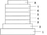
图1表示有机EL元件的一例的剖面图。FIG. 1 shows a cross-sectional view of an example of an organic EL element.
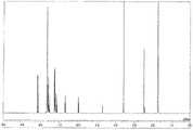
图2表示化合物1-1的1H-NMR图表。Fig. 2 shows a1 H-NMR chart of Compound 1-1.
图3表示化合物2-1的1H-NMR图表。Fig. 3 shows a1 H-NMR chart of compound 2-1.
图4表示化合物3-1的1H-NMR图表。Fig. 4 shows a1 H-NMR chart of compound 3-1.
具体实施方式Detailed ways
本发明的有机EL元件,在阳极和阴极之间夹持包含至少含空穴传输层、发光层的多个层的有机层。而且,与空穴传输层侧的发光层邻接而具有EB层,从EB来看在阳极侧配置空穴传输层。发光层含有磷光发光材料,EB层含有上述通式(1)表示的吲哚并咔唑化合物。In the organic EL device of the present invention, an organic layer including a plurality of layers including at least a hole transport layer and a light emitting layer is interposed between an anode and a cathode. Furthermore, an EB layer is provided adjacent to the light-emitting layer on the side of the hole transport layer, and the hole transport layer is disposed on the anode side when viewed from the EB. The light-emitting layer contains a phosphorescent light-emitting material, and the EB layer contains an indolocarbazole compound represented by the above general formula (1).
通式(1)所示的吲哚并咔唑化合物的若干已经在上述专利文献等中已知,但其使用形态不同。但是,如果为作为空穴传输性材料已知的吲哚并咔唑化合物,则可以有利地使用其。Some indolocarbazole compounds represented by the general formula (1) are already known in the above-mentioned patent documents and the like, but their usage forms are different. However, if it is an indolocarbazole compound known as a hole-transporting material, it can be advantageously used.
在本发明中使用的吲哚并咔唑化合物,在通式(1)中,Z表示n价的碳数6~50的芳香族烃基、碳数3~50的芳香族杂环基,n表示1~6的整数。Y表示具有式(1a)表示的吲哚并咔唑骨架的基团。这些芳香族烃基及芳香族杂环基可以具有取代基,也可以不具有取代基。In the indolocarbazole compound used in the present invention, in the general formula (1), Z represents an n-valent aromatic hydrocarbon group with 6 to 50 carbons and an aromatic heterocyclic group with 3 to 50 carbons, and n represents An integer of 1 to 6. Y represents a group having an indolocarbazole skeleton represented by formula (1a). These aromatic hydrocarbon groups and aromatic heterocyclic groups may or may not have a substituent.
作为不具有取代基的芳香族烃基及芳香族杂环基的优选具体例,可以举出从苯、吡啶、嘧啶、三嗪、吲哚、咔唑、萘、喹啉、异喹啉、喹喔啉、萘啶或连接有多个这些芳香环的芳香族化合物中除去n个氢而生成的n价基团,更优选可以举出从苯、吡啶、嘧啶、三嗪、吲哚、咔唑、萘、喹啉或连接有多个这些芳香环的芳香族化合物中除去n个氢而生成的n价基团。需要说明的是,在为由连接有多个芳香环的芳香族化合物生成的基团的情况下,连接的数优选为2~10,更优选为2~7。此时,与Y的连接位置没有限定,可以为末端的环,也可以为中央部的环。Preferable specific examples of aromatic hydrocarbon groups and aromatic heterocyclic groups without substituents include benzene, pyridine, pyrimidine, triazine, indole, carbazole, naphthalene, quinoline, isoquinoline, quinoxa N-valent groups formed by removing n hydrogens from lines, naphthyridines, or aromatic compounds connected with a plurality of these aromatic rings, more preferably benzene, pyridine, pyrimidine, triazine, indole, carbazole, An n-valent group formed by removing n hydrogens from naphthalene, quinoline, or an aromatic compound to which a plurality of these aromatic rings are linked. In addition, when it is a group produced|generated from the aromatic compound to which several aromatic rings were linked, the number of links is preferably 2-10, and it is more preferable that it is 2-7. At this time, the connection position to Y is not limited, and may be a terminal loop or a central loop.
其中,在由连接有多个芳香环的芳香族化合物生成的基团为2价的基团的情况下,例如,可由下述式所示。However, when the group produced from the aromatic compound which couple|bonded the several aromatic ring is a divalent group, it can be represented by the following formula, for example.

(Ar1~Ar6为无取代的单环或稠环的芳香环)(Ar1 to Ar6 are unsubstituted monocyclic or condensed aromatic rings)
作为从连接有多个上述芳香环的芳香族化合物中除去氢而生成的基团的具体例,可以举出例如从联苯、三联苯、联吡啶、联嘧啶、联三嗪、三联吡啶、双三嗪基苯、二咔唑基苯、咔唑基联苯、二咔唑基联苯、苯基三联苯、咔唑基三联苯、联萘、苯基吡啶、苯基咔唑、二苯基咔唑、二苯基吡啶、苯基嘧啶、二苯基嘧啶、苯基三嗪、二苯基三嗪、苯基萘、二苯基萘等中除去n个氢而生成的基团。Specific examples of groups formed by removing hydrogen from an aromatic compound to which a plurality of the above-mentioned aromatic rings are linked include biphenyl, terphenyl, bipyridine, bipyrimidine, bitriazine, terpyridine, bis Triazinylbenzene, biscarbazolylbenzene, carbazolylbiphenyl, dicarbazolylbiphenyl, phenyl terphenyl, carbazolyl terphenyl, binaphthyl, phenylpyridine, phenylcarbazole, diphenyl A group formed by removing n hydrogens from carbazole, diphenylpyridine, phenylpyrimidine, diphenylpyrimidine, phenyltriazine, diphenyltriazine, phenylnaphthalene, diphenylnaphthalene, etc.
在上述芳香族烃基或芳香族杂环基具有取代基的情况下,作为优选的取代基,有碳数1~4的烷基,碳数1~2的烷氧基、乙酰基,碳数6~24的二芳基氨基。更优选为甲基或二苯基氨基。另外,由连接有多个芳香环的芳香族化合物生成的基团也同样可以具有取代基。When the above-mentioned aromatic hydrocarbon group or aromatic heterocyclic group has a substituent, preferred substituents include an alkyl group having 1 to 4 carbons, an alkoxy group having 1 to 2 carbons, an acetyl group, and an acetyl group having 6 carbons. ~24 diarylamino groups. More preferred is methyl or diphenylamino. In addition, a group formed from an aromatic compound having a plurality of aromatic rings linked thereto may also have a substituent.
在上述芳香族烃基或芳香族杂环基具有取代基的情况下,取代基的总数为1~10。优选为1~6,更优选为1~4。另外,在上述芳香族烃基或芳香族杂环基具有2个以上的取代基的情况下,它们可以相同,也可以不同。另外,在上述芳香族烃基或芳香族杂环基的碳数的计算中,在具有取代基的情况下,包含其取代基的碳数。When the above-mentioned aromatic hydrocarbon group or aromatic heterocyclic group has a substituent, the total number of substituents is 1-10. Preferably it is 1-6, More preferably, it is 1-4. In addition, when the above-mentioned aromatic hydrocarbon group or aromatic heterocyclic group has two or more substituents, they may be the same or different. In addition, in the calculation of the carbon number of the above-mentioned aromatic hydrocarbon group or aromatic heterocyclic group, when it has a substituent, the carbon number of the substituent is included.
通式(1)中,n为1~6的整数,但优选为为1~4,更优选为1~3。In general formula (1), n is an integer of 1-6, Preferably it is 1-4, More preferably, it is 1-3.
通式(1)中,Y由式(1a)表示,式(1a)中的环A由式(1b)表示。式(1b)中,X为次甲基或氮。R3表示氢、碳数1~10的烷基族烃基、碳数6~12的芳香族烃基、碳数3~11的芳香族杂环基、或与含X的六元环缩合的基团。在R3为与含X的六元环进行缩合的基团的情况下,作为从缩合形成的稠环中除去含X的六元环的环,可以为吡咯环、呋喃环、噻吩环、吲哚环、苯并呋喃环、苯并噻吩环、苯环、萘环。这些环也可以具有取代基,优选的是为可以具有取代基的吲哚环,此时如果包含含有X的六元环则可以形成咔唑环。在R3与含X的六元环进行缩合的情况下,为R3在含X的六元环上进行取代的位置的邻接位的碳具有可取代的氢的情况,形成咔唑环的情况还限定在X为次甲基的情况。In general formula (1), Y is represented by formula (1a), and ring A in formula (1a) is represented by formula (1b). In formula (1b), X is methine or nitrogen. R3 represents hydrogen, an alkyl hydrocarbon group with 1 to 10 carbons, an aromatic hydrocarbon group with 6 to 12 carbons, an aromatic heterocyclic group with 3 to 11 carbons, or a group condensed with a six-membered ring containing X . In the case whereR3 is a group that condenses with a six-membered ring containing X, the ring that removes the six-membered ring containing X from the condensed ring formed by condensation may be a pyrrole ring, a furan ring, a thiophene ring, an ind Indole ring, benzofuran ring, benzothiophene ring, benzene ring, naphthalene ring. These rings may also have a substituent, preferably an indole ring which may have a substituent, and in this case, a carbazole ring may be formed if a six-membered ring containing X is included. In the case whereR3 is condensed with a six-membered ring containing X, when the carbon adjacent to the position whereR3 is substituted on the six-membered ring containing X has a substitutable hydrogen, a carbazole ring is formed It is also limited to the case where X is a methine group.
式(1a)中,环B由式(1c)表示。式(1c)中,Ar表示碳数6~50的芳香族烃基、碳数3~50的芳香族杂环基。这些芳香族烃基或芳香族杂环基可以具有取代基,也可以不具有取代基。这些芳香族烃基及芳香族杂环基的优选的例子,除了为1价的基团以外,与上述构成Z的芳香族烃基或芳香族杂环基相同。另外,式(1c)中的N与Ar的取代位置没有限定。In formula (1a), ring B is represented by formula (1c). In formula (1c), Ar represents an aromatic hydrocarbon group having 6 to 50 carbon atoms or an aromatic heterocyclic group having 3 to 50 carbon atoms. These aromatic hydrocarbon groups or aromatic heterocyclic groups may or may not have substituents. Preferred examples of these aromatic hydrocarbon groups and aromatic heterocyclic groups are the same as the above-mentioned aromatic hydrocarbon groups or aromatic heterocyclic groups constituting Z, except that they are monovalent groups. In addition, the substitution positions of N and Ar in the formula (1c) are not limited.
作为不具有取代基的芳香族烃基及芳香族杂环基的优选的具体例子,可以举出由苯、吡啶、嘧啶、三嗪、吲哚、咔唑、萘、喹啉、异喹啉、喹喔啉、萘啶产生的1价基团,更优选的是,可以举出苯、吡啶、嘧啶、三嗪、吲哚、咔唑或萘产生的1价基团。另外,也可以优选举出由连接有多个这些芳香环的芳香族化合物产生的1价基团,可以举出例如由联苯、三联苯、联吡啶、联嘧啶、联三嗪、三联吡啶、双三嗪基苯、二咔唑基苯、咔唑基联苯、二咔唑基联苯、苯基三联苯、咔唑基三联苯、联萘、苯基吡啶、苯基咔唑、二苯基咔唑、二苯基吡啶、苯基嘧啶、二苯基嘧啶、苯基三嗪、二苯基三嗪、苯基萘、二苯基萘等产生的1价基团。另外,在具有取代基的情况下,作为优选的取代基,为碳数1~4的烷基,碳数1~2的烷氧基、乙酰基或碳数6~24的二酰基氨基。更优选为甲基或二苯基氨基。Preferable specific examples of aromatic hydrocarbon groups and aromatic heterocyclic groups without substituents include benzene, pyridine, pyrimidine, triazine, indole, carbazole, naphthalene, quinoline, isoquinoline, quinoline, Monovalent groups derived from oxaline and naphthyridine, more preferably monovalent groups derived from benzene, pyridine, pyrimidine, triazine, indole, carbazole or naphthalene. In addition, a monovalent group derived from an aromatic compound to which a plurality of these aromatic rings are linked can also be preferably mentioned, such as biphenyl, terphenyl, bipyridine, bipyrimidine, bitriazine, terpyridine, Bis-triazinylbenzene, biscarbazolylbenzene, carbazolylbiphenyl, dicarbazolylbiphenyl, phenyl terphenyl, carbazolyl terphenyl, binaphthyl, phenylpyridine, phenylcarbazole, diphenyl Monovalent groups produced by carbazole, diphenylpyridine, phenylpyrimidine, diphenylpyrimidine, phenyltriazine, diphenyltriazine, phenylnaphthalene, diphenylnaphthalene, etc. Moreover, when it has a substituent, a preferable substituent is an alkyl group having 1 to 4 carbons, an alkoxy group having 1 to 2 carbons, an acetyl group, or a diacylamino group having 6 to 24 carbons. More preferred is methyl or diphenylamino.
式(1a)中,R1、R2分别独立地表示氢、碳数1~10的脂肪族烃基、碳数6~12的芳香族烃基或碳数3~11的芳香族杂环基。优选为氢、碳数1~4的烷基、苯基、吡啶基、嘧啶基、三嗪基、萘基、联苯基、联嘧啶基或咔唑基,更优选为氢、苯基或咔唑基。In formula (1a), R1 and R2 each independently represent hydrogen, an aliphatic hydrocarbon group having 1 to 10 carbons, an aromatic hydrocarbon group having 6 to 12 carbons, or an aromatic heterocyclic group having 3 to 11 carbons. Preferably hydrogen, alkyl with 1 to 4 carbons, phenyl, pyridyl, pyrimidyl, triazinyl, naphthyl, biphenyl, bipyrimidyl or carbazolyl, more preferably hydrogen, phenyl or carbazolyl Azolyl.
需要说明的是,在上述R1、R2及R3为碳数1~10的脂肪族烃基、碳数6~12的芳香族烃基或碳数3~11的芳香族杂环基的情况下,其各自优选的基团共通。It should be noted that, when the above-mentioned R1 , R2 and R3 are an aliphatic hydrocarbon group having 1 to 10 carbons, an aromatic hydrocarbon group having 6 to 12 carbons, or an aromatic heterocyclic group having 3 to 11 carbons , and their respective preferred groups are common.
作为上述通式(1)表示的吲哚并咔唑化合物,通式(2)表示的吲哚并咔唑化合物作为优选的。As the indolocarbazole compound represented by the above general formula (1), an indolocarbazole compound represented by the general formula (2) is preferable.
通式(2)中,环B表示与邻接环缩合的式(1c)表示的杂环。该环B或式(1c)具有与通式(1)的环B或式(1c)相同的含义。另外,Z、Ar、R1、R2具有通式(1)的Z、Ar、R1、R2相同的含义。R3表示氢、碳数1~10的烷基、碳数6~12的芳香族烃基、或碳数3~11的芳香族杂环基。其中,上述芳香族烃基及芳香族杂环基优选不是稠环结构。n表示1或2的整数。In general formula (2), ring B represents a heterocyclic ring represented by formula (1c) condensed with an adjacent ring. The ring B or the formula (1c) has the same meaning as the ring B of the general formula (1) or the formula (1c). In addition, Z, Ar, R1 and R2 have the same meanings as Z, Ar, R1 and R2 in the general formula (1). R3 represents hydrogen, an alkyl group having 1 to 10 carbons, an aromatic hydrocarbon group having 6 to 12 carbons, or an aromatic heterocyclic group having 3 to 11 carbons. Among them, the above-mentioned aromatic hydrocarbon group and aromatic heterocyclic group are preferably not condensed ring structures. n represents an integer of 1 or 2.
作为上述通式(2)表示的吲哚并咔唑化合物,通式(3)~(6)的任一式表示的吲哚并咔唑化合物作为优选的。As the indolocarbazole compound represented by the general formula (2), an indolocarbazole compound represented by any one of the general formulas (3) to (6) is preferable.
通式(3)~(6)中,Z、Ar、R1、R2、R3及n具有与通式(2)的那些相同的含义。In general formulas (3) to (6), Z, Ar, R1 , R2 , R3 and n have the same meanings as those of general formula (2).
通式(1)~(6)表示的吲哚并咔唑化合物,可以使用公知的手法进行合成。The indolocarbazole compounds represented by the general formulas (1) to (6) can be synthesized by known methods.
例如,通式(3)表示的吲哚并咔唑化合物的吲哚并咔唑骨架,以Synlett,2005,No.1,p42-48所示的合成例为参考通过以下的反应式来进行合成。For example, the indolocarbazole skeleton of the indolocarbazole compound represented by general formula (3) is synthesized by the following reaction formula with reference to the synthesis example shown in Synlett, 2005, No.1, p42-48 .

另外,通式(4)及通式(5)表示的吲哚并咔唑骨架,可以以TheJournal of Organic Chemistry,2007,72(15)5886以及Tetrahedron,1999,55,p2371所示的合成例为参考通过以下的反应式来进行合成。In addition, the indolocarbazole skeleton represented by the general formula (4) and the general formula (5) can be synthesized as shown in TheJournal of Organic Chemistry, 2007, 72 (15) 5886 and Tetrahedron, 1999, 55, p2371 as Refer to the following reaction formula to synthesize.

进而,通式(6)表示的吲哚并咔唑骨架,可以以ArchivderPharmazie(Weinheim,Germany),1987,320(3),p280-2所示的合成例为参考通过以下的反应式来进行合成。Furthermore, the indolocarbazole skeleton represented by general formula (6) can be synthesized by the following reaction formula with reference to the synthesis example shown in Archivder Pharmazie (Weinheim, Germany), 1987, 320 (3), p280-2 .

可以通过使上述的反应式得到的各吲哚并咔唑与对应的卤素取代芳香族化合物等进行偶联反应,在存在于吲哚并咔唑骨架中的2个氮上进行取代的氢被取代为芳香族基团,合成通式(1)~(6)表示的本发明的吲哚并咔唑化合物。Each indolocarbazole obtained by the above reaction formula can be subjected to a coupling reaction with a corresponding halogen-substituted aromatic compound, etc., and the hydrogens that are substituted on the two nitrogens existing in the indolocarbazole skeleton are substituted The indolocarbazole compounds of the present invention represented by general formulas (1) to (6) are synthesized as aromatic groups.
以下示出通式(1)~(6)表示的吲哚并咔唑化合物的优选具体例,但本发明使用的吲哚并咔化合物不限定于这些具体例。Preferred specific examples of indolocarbazole compounds represented by general formulas (1) to (6) are shown below, but the indolocarbazole compounds used in the present invention are not limited to these specific examples.


本发明的有机EL元件,在阳极和阴极之间夹持含空穴传输层和发光层的有机层而成,在发光层中含有磷光发光材料,在空穴传输层和发光层之间具有与发光层邻接而含有通式(1)表示的吲哚并咔唑化合物的EB层。The organic EL element of the present invention is formed by sandwiching an organic layer containing a hole transport layer and a light-emitting layer between the anode and the cathode, the light-emitting layer contains a phosphorescent light-emitting material, and has a The light-emitting layer is adjacent to the EB layer containing the indolocarbazole compound represented by the general formula (1).
其中,已知在空穴传输层的空穴传输性材料、发光层的主体材料中使用通式(1)表示的吲哚并咔唑化合物中所含的一部分的化合物,但在本发明中,在空穴传输层和发光层之间设置上述EB层。而且,在与EB分开设置的空穴传输性层中使用的材料使用具有比在EB层中使用的吲哚并咔唑化合物的HOMO能量大的HOMO能量的空穴传输性材料,优选使用吲哚并咔唑化合物以外的空穴传输性材料。Among them, it is known to use a part of the compounds contained in the indolocarbazole compound represented by the general formula (1) in the hole-transporting material of the hole-transporting layer and the host material of the light-emitting layer, but in the present invention, The above-mentioned EB layer is provided between the hole transport layer and the light emitting layer. Furthermore, the material used in the hole-transporting layer provided separately from EB uses a hole-transporting material having a HOMO energy greater than that of the indolocarbazole compound used in the EB layer, preferably indole Hole-transporting materials other than carbazole compounds.
优选EB层的邻接层之一为发光层,另一层为含空穴传输层或空穴传输性材料的层。在此,由于在EB层和阳极之间配置的含空穴传输性材料的层也作为空穴传输层发挥功能,因此在本发明书中该层也称为空穴传输层。因此,空穴传输层可以为1层,也可以为2层以上。Preferably, one of the adjacent layers of the EB layer is a light-emitting layer, and the other layer is a layer containing a hole-transporting layer or a hole-transporting material. Here, since the layer containing the hole-transporting material disposed between the EB layer and the anode also functions as a hole-transporting layer, this layer is also referred to as a hole-transporting layer in the present specification. Therefore, the hole transport layer may be one layer, or may be two or more layers.
优选在EB层中所含有的吲哚并咔唑化合物的LUMO能量比邻接的发光层中所含的化合物的LUMO能量大。在邻接的发光层含有多种化合物的情况下,优选比作为其主成分的化合物大。吲哚并咔唑化合物的LUMO能量比发光层中所含的化合物(主成分)的LUMO能量大0.1eV以上、优选大0.3eV以上、进一步优选大0.5eV以上为宜。Preferably, the LUMO energy of the indolocarbazole compound contained in the EB layer is larger than the LUMO energy of the compound contained in the adjacent light-emitting layer. When the adjacent light-emitting layer contains a plurality of compounds, it is preferably larger than the compound that is its main component. The LUMO energy of the indolocarbazole compound is preferably greater than that of the compound (main component) contained in the light-emitting layer by 0.1 eV or more, preferably 0.3 eV or more, more preferably 0.5 eV or more.
吲哚并咔唑化合物的LUMO能量优选为-1.2eV以上,更优选为-1.0eV以上,最优选-0.9eV以上。The LUMO energy of the indolocarbazole compound is preferably -1.2 eV or higher, more preferably -1.0 eV or higher, and most preferably -0.9 eV or higher.
另外,优选空穴传输层中含有的空穴传输性材料的HOMO能量比上述通式(1)表示的吲哚并咔唑化合物的HOMO能量大。另外,虽然没有特别限定,但与阳极或空穴注入层邻接的空穴传输材料的HOMO能量优选为-4.8eV以上。In addition, it is preferable that the HOMO energy of the hole-transporting material contained in the hole-transporting layer is larger than the HOMO energy of the indolocarbazole compound represented by the above general formula (1). In addition, although not particularly limited, the HOMO energy of the hole transport material adjacent to the anode or the hole injection layer is preferably -4.8 eV or more.
作为本发明的有机EL元件的优选方式,发光层含有至少一种磷光发光材料和至少一种电子传输性主体材料。此时,流过发光层中的电子被EBL有效地阻挡,降低电子向空穴传输层的泄露。由此,发光层中的空穴与电子的复合概率提高,磷光发光材料的发光效率提高。In a preferred embodiment of the organic EL device of the present invention, the light-emitting layer contains at least one phosphorescent material and at least one electron-transporting host material. At this time, the electrons flowing through the light-emitting layer are effectively blocked by the EBL, reducing the leakage of electrons to the hole transport layer. As a result, the recombination probability of holes and electrons in the light-emitting layer increases, and the light-emitting efficiency of the phosphorescent light-emitting material increases.
作为更优选的有机EL元件的方式,除上述以外,在阴极和发光层之间具有电子传输层。作为用于电子传输层的材料的优选的电子移动速度,为1×10⁻⁷cm2/V·s以上,更优选为1×10-6cm2/V·s以上,最优选为1×10-5cm2/V·s以上。As a more preferable aspect of the organic EL element, in addition to the above, an electron transport layer is provided between the cathode and the light emitting layer. The preferred electron movement speed of the material used for the electron transport layer is 1×10⁻⁷ cm2 /V·s or more, more preferably 1×10 -6
需要说明的是,本发明书所谓的LUMO能量及HOMO能量的值,为使用美国Gaussian公司制的分子轨道计算用软件即Gaussian03而求得的值,定义为通过B3LYP/6-31G*水平的结构最优化计算而算出的值。It should be noted that the values of LUMO energy and HOMO energy referred to in this specification are values obtained using Gaussian03, a software for molecular orbital calculations manufactured by Gaussian Corporation of the United States, and are defined as structures passing through the B3LYP/6-31G* level The value calculated by the optimization calculation.
另外,本发明书所谓的电子移动速度的值,为用Time Of Fright(TOF)法测定的电场E1/2=500(V/cm)1/2时的值。In addition, the value of electron movement speed referred to in this specification is the value when the electric field E1/2 = 500 (V/cm)1/2 measured by the Time Of Fright (TOF) method.
接着,一边参照附图一边对本发明的有机EL元件的结构进行说明,但本发明的有机EL元件的结构并不限定于任何图示的结构。Next, the structure of the organic EL element of the present invention will be described with reference to the drawings, but the structure of the organic EL element of the present invention is not limited to any of the illustrated structures.
图1是示意性地表示用于本发明的一般的有机EL元件的结构例的剖面图,分别为1表示基板,2表示阳极,3表示空穴注入层,4表示空穴传输层,5表示EB层,6表示发光层,7表示电子传输层,8表示阴极。本发明的有机EL元件中,具有阳极、空穴传输层、EB层、发光层及阴极作为必须的层。有利的是,具有阳极、空穴传输层、EB层、发光层、电子传输层及阴极。1 is a cross-sectional view schematically showing a structural example of a general organic EL element used in the present invention, where 1 denotes a substrate, 2 denotes an anode, 3 denotes a hole injection layer, 4 denotes a hole transport layer, and 5 denotes a In the EB layer, 6 represents the light-emitting layer, 7 represents the electron transport layer, and 8 represents the cathode. The organic EL device of the present invention has an anode, a hole transport layer, an EB layer, a light emitting layer, and a cathode as essential layers. It is advantageous to have an anode, a hole transport layer, an EB layer, an emitting layer, an electron transport layer and a cathode.
另外,本发明的有机EL元件也可以在必须的层以外的层中具有电子传输层、电子注入层、空穴阻挡层。进而,空穴传输层也可以为具有空穴注入功能的空穴注入传输层,电子传输层也可以为具有电子注入功能的电子注入传输层。In addition, the organic EL device of the present invention may have an electron transport layer, an electron injection layer, and a hole blocking layer in layers other than the essential layers. Furthermore, the hole transport layer may be a hole injection transport layer having a hole injection function, and the electron transport layer may also be an electron injection transport layer having an electron injection function.
需要说明的是,本发明的有机EL元件,也可以为与图1相反的结构,即,可在基板1上依次层叠阴极8、电子传输层7、发光层6、EB层5、空穴传输层4、阳极2,此时,也可以根据需要追加层或省略层。It should be noted that the organic EL element of the present invention can also have a structure opposite to that of FIG.
以下,对各部件及各层进行说明。Each member and each layer will be described below.
-基板--Substrate-
本发明的有机EL元件,优选被支承于基板上。对于该基板,没有特别的限定,为以往有机EL元件中常用的基板即可,例如可以使用由玻璃、透明塑料、石英等构成的基板。The organic EL element of the present invention is preferably supported on a substrate. The substrate is not particularly limited, and it may be a substrate commonly used in conventional organic EL elements. For example, a substrate made of glass, transparent plastic, quartz, or the like can be used.
-阳极--anode-
作为有机EL元件中的阳极,优选使用以功能函数大的(4eV以上)金属、合金、电传导性化合物及这些的混合物作为电极物质的阳极。作为这样的电极物质的具体例,可以举出Au等的金属、CuI、铟锡氧化物(ITO)、SnO2、ZnO等的导电性透明材料。另外,也可以使用IDIXO(In2O3-ZnO)等可以制作非晶质透明导电膜的材料。另外,对阳极而言,可以将这些电极物质通过蒸镀、溅射等的方法,形成薄膜,用光刻法形成所需的形状的图案,或者在不大需要图案精度的情况下(100μm以上左右),也可以在上述电极物质的蒸镀、溅射时经由所期望的形状的掩膜形成图案。或者,使用有机导电性化合物这样的可涂布物质的情况下,也可以使用印刷方式、涂敷方式等的湿式成膜法。在由该阳极取得发光的情况下,优选使透过率大于10%,另外,作为阳极的薄层电阻优选为数百Ω/□以下。进而膜厚也取决于材料,但通常在10~1000nm、优选在10~200nm的范围选择。As the anode in the organic EL element, it is preferable to use an anode having a large functional function (4 eV or more), a metal, an alloy, an electrically conductive compound, or a mixture thereof as an electrode substance. Specific examples of such an electrode substance include metals such as Au, and conductive transparent materials such as CuI, indium tin oxide (ITO), SnO2 , and ZnO. In addition, a material capable of forming an amorphous transparent conductive film such as IDIXO (In2 O3 -ZnO) may be used. In addition, for the anode, these electrode substances can be formed into a thin film by evaporation, sputtering, etc., and a pattern of the desired shape can be formed by photolithography, or when the pattern accuracy is not required (more than 100 μm) left and right), and patterning may be formed through a mask of a desired shape during vapor deposition and sputtering of the above-mentioned electrode material. Alternatively, when a coatable substance such as an organic conductive compound is used, a wet film-forming method such as a printing method or a coating method may be used. When light emission is obtained from the anode, the transmittance is preferably greater than 10%, and the sheet resistance of the anode is preferably several hundred Ω/□ or less. Furthermore, the film thickness also depends on the material, but is usually selected within a range of 10 to 1000 nm, preferably 10 to 200 nm.
-阴极--cathode-
另一方面,作为阴极,可以使用以功能函数小的(4eV以下)金属(称为电子注入性金属)、合金、电传导性化合物及这些的混合物作为电极物质的阴极。作为这样的电极物质的具体例,可以举出钠、钠-钾合金、镁、锂、镁/铜混合物、镁/银混合物、镁/铝混合物、镁/铟混合物、铝/氧化铝(Al2O3)混合物、铟、锂/铝混合物、稀土类金属等。其中,从电子注入性及对氧化等的耐久性的方面考虑,电子注入性金属和功能函数的值比其大的稳定的金属即第二金属的混合物,例如,镁/银混合物、镁/铝混合物、镁/铟混合物、铝/氧化铝(Al2O3)混合物、锂/铝混合物、铝等是优选的。阴极可以通过将这些电极物质通过蒸镀、溅射等的方法形成薄膜,由此进行制作。另外,作为阴极的薄层电阻优选为数百Ω/□以下,膜厚通常在10nm~5μm、优选在50~200nm的范围选择。需要说明的是,为了使发出的光透过,有机EL元件的阳极或阴极的任一者为透明或半透明。On the other hand, as the cathode, a metal having a small functional function (4 eV or less) (called an electron-injecting metal), an alloy, an electrically conductive compound, or a mixture thereof as an electrode substance can be used. Specific examples of such electrode materials include sodium, sodium-potassium alloys, magnesium, lithium, magnesium/copper mixtures, magnesium/silver mixtures, magnesium/aluminum mixtures, magnesium/indium mixtures, aluminum/alumina (Al2 O3 ) mixtures, indium, lithium/aluminum mixtures, rare earth metals, etc. Among them, from the viewpoint of electron injectability and durability against oxidation, etc., a mixture of an electron injectable metal and a stable metal having a function function larger than it, that is, a second metal, for example, a magnesium/silver mixture, magnesium/aluminum Mixtures, magnesium/indium mixtures, aluminum/alumina (Al2 O3 ) mixtures, lithium/aluminum mixtures, aluminum, and the like are preferred. The cathode can be produced by forming a thin film of these electrode substances by vapor deposition, sputtering, or the like. In addition, the sheet resistance of the cathode is preferably several hundred Ω/□ or less, and the film thickness is usually selected in the range of 10 nm to 5 μm, preferably 50 to 200 nm. In addition, in order to transmit emitted light, either the anode or the cathode of an organic EL element is transparent or translucent.
另外,通过在阴极中使用在阳极的说明中举出的导电性透明材料,可以制作透明或半透明的阴极,通过应用这些导电性透明材料可以制作阳极和阴极两者具有透过性的元件。In addition, by using the conductive transparent material mentioned in the description of the anode for the cathode, a transparent or translucent cathode can be produced, and by using these conductive transparent materials, an element having both the anode and the cathode can be produced.
-发光层--Emitting layer-
发光层为磷光发光层,含有磷光发光材料和主体材料。作为发光层中的磷光发光材料,为含有包含选自钌、铑、钯、银、铼、锇、铱、白金及金中的至少一种的金属的有机金属络合物即可。该有机金属络合物,在上述专利文献等中是公知的,可以选择使用这些有机金属络合物。The light-emitting layer is a phosphorescent light-emitting layer, which contains phosphorescent light-emitting materials and host materials. The phosphorescent material in the light emitting layer may be an organometallic complex containing at least one metal selected from the group consisting of ruthenium, rhodium, palladium, silver, rhenium, osmium, iridium, platinum and gold. Such organometallic complexes are known in the above-mentioned patent documents and the like, and these organometallic complexes can be selected and used.
作为优选的磷光发光材料,可以举出具有Ir等贵的金属元素作为中心金属的Ir(ppy)3等的络合物类、Ir(bt)2·acac3等的络合物类、PtOEt3等的络合物类。将这些络合物类的具体例示于以下,但并不限定于下述化合物。Preferable phosphorescent luminescent materials include complexes such as Ir(ppy)3, complexes such as Ir(bt)2.acac3, and PtOEt3 having a noble metal element such as Ir as a central metal. Complexes. Specific examples of these complexes are shown below, but are not limited to the following compounds.


上述磷光发光材料在发光层中所含有的量在1~20重量%、优选在5~10重量%的范围即可。The amount of the above-mentioned phosphorescent light-emitting material contained in the light-emitting layer may be in the range of 1 to 20% by weight, preferably in the range of 5 to 10% by weight.
发光层中的主体材料,通过许多的专利文献等而得知,因此可以从中选择。作为主体材料的具体例,没有特别的限定,可以举出吲哚衍生物、咔唑衍生物、吲哚并咔唑衍生物、三唑衍生物、唑衍生物、二唑衍生物、咪唑衍生物、聚芳基烷烃衍生物、吡唑啉衍生物、吡唑啉酮衍生物、苯二胺衍生物、芳基胺衍生物、氨基取代查尔酮衍生物、苯乙烯基蒽衍生物、芴酮衍生物、腙衍生物、芪衍生物、硅氮烷衍生物、芳香族叔胺化合物、苯乙烯基胺化合物、芳香族二亚甲基系化合物、卟啉系化合物、蒽醌二甲烷衍生物、蒽酮衍生物、二苯基苯醌衍生物、硫代吡喃二氧化物衍生物、萘并苝等杂环四甲酸酐、酞菁衍生物、以8-喹啉衍生物的金属络合物或金属酞菁、苯并
一般而言,主体材料具有空穴和电子的两电荷的传输能,特别是将空穴传输性能优异的材料称为空穴传输性主体材料,另外将电子传输能优异的材料称为电子传输性主体材料。In general, a host material has the ability to transport two charges of holes and electrons. In particular, a material with excellent hole-transport performance is called a hole-transport host material, and a material with excellent electron-transport performance is called an electron-transport host material. Body material.
在本发明的有机EL元件中,优选使用电子传输性主体材料。本说明书中所谓的电子传输性主体材料,定义为电子移动速度比空穴移动速度大的主体材料、或电子移动速度为1×10⁻⁷cm2/V·s以上的主体材料。特别优选电子传输性主体材料的电子移动速度为1×10-6cm2/V·s以上。In the organic EL device of the present invention, an electron-transporting host material is preferably used. The term "electron-transporting host material" in this specification is defined as a host material whose electron movement speed is higher than that of holes, or a host material whose electron movement speed is 1×10⁻⁷ cm2 /V·s or more. It is particularly preferable that the electron transport velocity of the electron-transporting host material is 1×10⁻⁶ cm2 /V·s or more.
作为具体的电子传输性主体材料,可以举出咔唑衍生物、吲哚并咔唑衍生物、吡啶、嘧啶、三嗪、咪唑衍生物、吡唑、三唑衍生物、


-注入层--injection layer-
注入层是指为了驱动电压的降低、发光亮度的提高而在电极和有机层之间设置的层,具有空穴注入层和电子注入层,可以存在于阳极和发光层或空穴传输层之间、及在阴极和发光层或电子传输层之间。注入层可以根据需要设置。The injection layer refers to the layer arranged between the electrode and the organic layer for the purpose of reducing the driving voltage and improving the luminous brightness. It has a hole injection layer and an electron injection layer, and can exist between the anode and the light emitting layer or the hole transport layer. , and between the cathode and the light emitting layer or electron transport layer. The injection layer can be set as needed.
-阻挡层--Barrier layer-
阻挡层可以阻止存在于发光层中的电荷(电子或空穴)及/或激子向发光层外的扩散。电子阻挡层可以配置在发光层及空穴传输层之间,阻止电子朝向空穴传输层的方向通过发光层。同样,空穴阻挡层可以配置在发光层及电子传输层之间,阻止空穴朝向电子传输层的方向通过发光层。阻挡层另外还可以用于阻止激子扩散至发光层的外侧而使用。即电子阻挡层、空穴阻挡层也可以分别兼备作为激子阻挡层的功能。本说明书中所谓的EB层,以为一层含有具有电子阻挡层及/或激子阻挡层功能的层而使用。The blocking layer can prevent charges (electrons or holes) and/or excitons present in the light emitting layer from diffusing out of the light emitting layer. The electron blocking layer can be disposed between the light-emitting layer and the hole transport layer to prevent electrons from passing through the light-emitting layer toward the hole transport layer. Likewise, the hole blocking layer can be disposed between the light emitting layer and the electron transport layer, preventing holes from passing through the light emitting layer toward the electron transport layer. The barrier layer can also be used to prevent excitons from diffusing to the outside of the light emitting layer. That is, the electron blocking layer and the hole blocking layer may each have a function as an exciton blocking layer. The EB layer referred to in this specification is used for one layer including a layer having the function of an electron blocking layer and/or an exciton blocking layer.
-空穴阻挡层--Hole blocking layer-
空穴阻挡层具有一边传输电子一边阻止空穴到达电子传输层的作用,由此可以使在发光层中的电子和空穴的复合概率提高。作为空穴阻挡层的材料,可以举出铝金属络合物、苯乙烯基衍生物、三唑衍生物、菲咯啉衍生物、
-电子阻挡层--Electron blocking layer-
电子阻挡层具有一边传输空穴一边阻止电子到达空穴传输层的作用,由此可以使在发光层中的电子和空穴的复合概率提高。The electron blocking layer has a function of preventing electrons from reaching the hole transporting layer while transporting holes, thereby improving the recombination probability of electrons and holes in the light emitting layer.
作为电子阻挡层的材料,优选使用通式(1)表示的吲哚并咔唑化合物。As a material for the electron blocking layer, an indolocarbazole compound represented by the general formula (1) is preferably used.
-激子阻挡层--Exciton blocking layer-
激子阻挡层为用于阻止因在发光层内空穴和电子复合而产生的激子扩散至电荷传输层的层,通过本层的插入可以有效地将激子约束在发光层内,可以使元件的发光效率提高。激子阻挡层可以邻接于发光层而插入阳极侧、阴极侧的任意一侧,也可以同时插入两侧。即,在阳极侧具有激子阻挡层的情况下,可以在空穴传输层和发光层之间与发光层邻接而插入该层,在插入于阴极侧的情况下,可以在发光层和阴极之间与发光层邻接而插入该层。另外,可以在阳极和与发光层的阳极侧邻接的激子阻挡层之间具有空穴注入层、电子阻挡层等,可以在阴极和与发光层的阴极侧邻接的激子阻挡层之间具有电子注入层、电子传输层、空穴阻挡层等。The exciton blocking layer is a layer used to prevent the excitons generated by the recombination of holes and electrons in the light-emitting layer from diffusing to the charge transport layer. The insertion of this layer can effectively confine the excitons in the light-emitting layer, which can make The luminous efficiency of the element is improved. The exciton blocking layer may be inserted adjacent to the light emitting layer on either the anode side or the cathode side, or may be inserted on both sides at the same time. That is, when there is an exciton blocking layer on the anode side, the layer can be inserted adjacent to the light-emitting layer between the hole transport layer and the light-emitting layer, and when it is inserted on the cathode side, it can be inserted between the light-emitting layer and the cathode. This layer is inserted adjacent to the light-emitting layer. In addition, a hole injection layer, an electron blocking layer, etc. may be provided between the anode and the exciton blocking layer adjacent to the anode side of the light-emitting layer, and an exciton blocking layer may be provided between the cathode and the exciton blocking layer adjacent to the cathode side of the light-emitting layer. Electron injection layer, electron transport layer, hole blocking layer, etc.
本发明涉及的EB层,由于作为电子阻挡层及/或激子阻挡层发挥功能,因此在发光层和阳极之间除EB层以外不设置电子阻挡层及激子阻挡层是有利的。需要说明的是,可以在发光层和阴极之间根据需要设置。EB层的膜厚优选为3~100nm,更优选为5~30nm。Since the EB layer according to the present invention functions as an electron blocking layer and/or an exciton blocking layer, it is advantageous not to provide an electron blocking layer and an exciton blocking layer other than the EB layer between the light emitting layer and the anode. It should be noted that it can be provided between the light-emitting layer and the cathode as needed. The film thickness of the EB layer is preferably 3 to 100 nm, more preferably 5 to 30 nm.
作为激子阻挡层的材料,优选使用通式(1)表示的吲哚并咔唑化合物,该衍生物更优选作为阳极侧的激子阻挡层来使用,但也可以为其它公知的激子阻挡材料。As the material of the exciton blocking layer, the indolocarbazole compound represented by the general formula (1) is preferably used, and the derivative is more preferably used as the exciton blocking layer on the anode side, but other known exciton blocking layers may also be used. Material.
作为可以使用的公知的激子阻止层用材料,例如可以举出1,3-二咔唑基苯(mCP)、双(2-甲基-8-羟基喹啉)-4-联苯羟基铝(III)(BAlq)。Known materials for the exciton blocking layer that can be used include, for example, 1,3-dicarbazolylbenzene (mCP), bis(2-methyl-8-quinolinol)-4-biphenylhydroxyaluminum (III) (BAlq).
-空穴传输层--Hole transport layer-
空穴传输层包含具有传输空穴功能的空穴传输材料,空穴传输层可以设置单层或多层。空穴传输层设置于EB层与阳极之间,含有空穴传输材料。空穴传输层优选与阳极或空穴注入层邻接。The hole transport layer includes a hole transport material having the function of transporting holes, and the hole transport layer can be provided as a single layer or multiple layers. The hole transport layer is disposed between the EB layer and the anode, and contains a hole transport material. The hole transport layer preferably adjoins the anode or the hole injection layer.
作为空穴传输材料,具有空穴的传输功能,也可以兼备注入功能。作为空穴传输材料。可以为有机物、无机物的任意一种。作为可以使用的公知的空穴传输材料,例如可以举出三唑衍生物、

EB层中含有的吲哚并咔唑化合物也为空穴传输材料的一种,但通过将含有该化合物的层与空穴传输层分开配置于发光层侧,可以作为EB层发挥功能。The indolocarbazole compound contained in the EB layer is also a type of hole transport material, but it can function as the EB layer by arranging a layer containing this compound on the side of the light emitting layer separately from the hole transport layer.
已知有使用了2层以上的空穴传输层的有机EL元件,但未知将吲哚并咔唑化合物如在本发明的有机EL元件中的EB层这样的位置进行配置而使用的例子。而且,通过设置上述EB层,显示出迄今为止没有的显著效果。认为,对显示出该优异效果的EB层而言,利用大的LUMO能量的优异的电子阻挡效果、适度的HOMO能量和空穴传输能力防止电子或激子从发光层泄露,可以赋予稳定、良好的元件特性。即使为已知有多种空穴传输材料的状况,也未知赋予这样的良好的元件特性的EB层用的化合物,为本发明人等首次发现。需要说明的是,在通常的空穴传输层中含有上述吲哚并咔唑化合物的情况下,空穴传输层为单层时,则有HOMO能量不适当,驱动电压高电压化,短寿命的趋势。An organic EL device using two or more hole transport layers is known, but an example in which an indolocarbazole compound is arranged and used at a position such as the EB layer in the organic EL device of the present invention is not known. Furthermore, by providing the above-mentioned EB layer, a remarkable effect that has not been seen so far is exhibited. It is considered that for the EB layer showing this excellent effect, the excellent electron blocking effect of large LUMO energy, moderate HOMO energy, and hole transport ability prevent leakage of electrons or excitons from the light-emitting layer, and can impart stable, good component characteristics. Even though many kinds of hole transport materials are known, there is no known compound for the EB layer that imparts such favorable device characteristics, and it was discovered by the present inventors for the first time. In addition, in the case where the above-mentioned indolocarbazole compound is contained in a normal hole transport layer, when the hole transport layer is a single layer, the HOMO energy is not appropriate, the driving voltage is increased, and the lifetime is short. trend.
-电子传输层--Electron transport layer-
电子传输层包含具有传输电子的功能的材料,电子传输层可以设置单层或多层。The electron transport layer contains a material having the function of transporting electrons, and the electron transport layer may be provided in a single layer or in multiple layers.
作为电子传输材料,只要具有将由阴极注入的电子传达到发光层的功能即可。作为可以使用的电子传输层,例如可以举出以Alq3为代表的铝络合物类、硝基取代芴衍生物、二苯基苯醌衍生物、硫代吡喃二氧化物衍生物、碳化二亚胺、亚芴基甲烷衍生物、蒽醌二甲烷及蒽酮衍生物、


-EB层--EB layer-
EB层为具有电子阻挡层、激子阻挡层或两者的功能的层,含有通式(1)表示的吲哚并咔唑化合物。The EB layer is a layer having the function of an electron blocking layer, an exciton blocking layer, or both, and contains an indolocarbazole compound represented by the general formula (1).
本发明的有机EL元件,可以为单一的元件、由阵列状配置的结构构成的元件、阳极和阴极以X-Y矩阵状配置的结构中的任意一种。本发明的有机EL元件,与发光层邻接、在空穴传输层和磷光发光层之间设置EB层,由此可以阻止电子及/或激子从发光层向空穴传输层的泄露,可以得到与以往的元件相比发光效率高且在驱动稳定方面也得到大大改善了的元件。The organic EL element of the present invention may be any of a single element, an element having a structure arranged in an array, and a structure in which anodes and cathodes are arranged in an X-Y matrix. In the organic EL element of the present invention, the EB layer is provided adjacent to the light-emitting layer and between the hole transport layer and the phosphorescent light-emitting layer, thereby preventing leakage of electrons and/or excitons from the light-emitting layer to the hole transport layer, and can obtain Compared with conventional devices, it has high luminous efficiency and greatly improved drive stability.
实施例Example
以下,通过实施例进一步详细地说明本发明,但本发明当然并不限定于这些实施例,只要不超出本发明的主旨,就可以以各种方式实施。Hereinafter, the present invention will be described in more detail by way of examples, but the present invention is of course not limited to these examples, and can be implemented in various forms as long as the gist of the present invention is not exceeded.
以下示出本发明化合物的合成例。需要说明的是,化合物编号对应上述化学式所带的编号。Synthesis examples of the compounds of the present invention are shown below. It should be noted that the compound numbers correspond to the numbers attached to the above chemical formulas.
合成例1Synthesis Example 1
化合物1-1的合成Synthesis of compound 1-1

在氮气氛下,将吲哚20.0g(0.17mol)的脱水乙醚300ml溶液在室温下一边搅拌一边在浓硫酸211.7g(2.16mol)中用1小时滴加浓盐酸112.0g(1.10mol),吹入产生的氯化氢气体。将反应溶液在室温下搅拌15小时后,添加醋酸乙酯121.0g和饱和碳酸氢钠水溶液303.2g。将水层用醋酸乙酯(2×100ml)萃取后,将有机层用饱和碳酸氢钠水溶液(100ml)和蒸馏水(2×100ml)清洗。将有机层用无水硫酸镁干燥后,过滤分离硫酸镁,减压蒸馏除去溶剂。将得到的残渣溶解在甲苯150ml中,加入钯/活性炭2.5g后,在111℃下一边加热回流一边搅拌3小时。将反应溶液冷却至室温后,过滤分离钯/活性炭,减压蒸馏除去溶剂。通过再结晶进行精制,得到作为白色结晶的中间体A 14.7g(收率37%)。Under a nitrogen atmosphere, 20.0 g (0.17 mol) of indole in dehydrated ether 300 ml solution was stirred at room temperature while adding 112.0 g (1.10 mol) of concentrated hydrochloric acid dropwise in 211.7 g (2.16 mol) of concentrated sulfuric acid in 1 hour, blowing into the hydrogen chloride gas produced. After stirring the reaction solution at room temperature for 15 hours, 121.0 g of ethyl acetate and 303.2 g of saturated aqueous sodium bicarbonate solution were added. After the aqueous layer was extracted with ethyl acetate (2×100 ml), the organic layer was washed with saturated aqueous sodium bicarbonate (100 ml) and distilled water (2×100 ml). After the organic layer was dried over anhydrous magnesium sulfate, the magnesium sulfate was separated by filtration, and the solvent was distilled off under reduced pressure. The obtained residue was dissolved in 150 ml of toluene, and after adding 2.5 g of palladium/activated carbon, the mixture was stirred at 111° C. under reflux for 3 hours. After cooling the reaction solution to room temperature, the palladium/activated carbon was separated by filtration, and the solvent was distilled off under reduced pressure. Purification was carried out by recrystallization to obtain 14.7 g of Intermediate A as white crystals (yield 37%).

在氮气氛下,将中间体A 14.1g(0.061mol)、N,N-二甲基氨基乙醛二乙基乙缩醛11.4g(0.071mol)和醋酸110.0g在118℃下一边加热回流一边搅拌8小时。将反应溶液冷却至室温后,滤取析出的结晶,用醋酸(30ml)清洗。将得到的结晶再浆液(reslurry)精制,得到作为白色结晶的中间体B 10.4g(收率67%)。Under a nitrogen atmosphere, 14.1 g (0.061 mol) of intermediate A, 11.4 g (0.071 mol) of N, N-dimethylaminoacetaldehyde diethyl acetal and 110.0 g of acetic acid were heated to reflux at 118 ° C. Stir for 8 hours. After cooling the reaction solution to room temperature, the precipitated crystals were collected by filtration and washed with acetic acid (30 ml). The obtained crystals were reslurry-purified to obtain 10.4 g of intermediate B as white crystals (yield 67%).

在氮气氛下,将中间体B 10.0g(0.039mol)、碘代苯79.6g(0.39mol)、铜12.4g(0.20mol)、碳酸钾16.2g(0.12mol)和四乙二醇二甲醚200ml在190℃下一边加热一边搅拌72小时。将反应溶液冷却至室温,过滤分离无机物后,在该溶液中一边搅拌一边加入蒸馏水(200ml),滤取析出的结晶。通过硅胶柱色谱法进行精制,得到作为白色固体的化合物1-110.0g(收率65%)。将熔点176℃、APCI-TOFMS,m/z 409[M+H]+、1H-NMR测定结果(测定溶剂:THF-d8)示于图2。Under nitrogen atmosphere, intermediate B 10.0g (0.039mol), iodobenzene 79.6g (0.39mol), copper 12.4g (0.20mol), potassium carbonate 16.2g (0.12mol) and tetraethylene glycol dimethyl ether 200 ml was stirred while heating at 190° C. for 72 hours. The reaction solution was cooled to room temperature, and after the inorganic matter was separated by filtration, distilled water (200 ml) was added to the solution while stirring, and the precipitated crystals were collected by filtration. Purification was carried out by silica gel column chromatography to obtain 10.0 g of Compound 1-11 as a white solid (yield 65%). Fig. 2 shows melting point 176°C, APCI-TOFMS, m/z 409 [M+H]+ , and1 H-NMR measurement results (measurement solvent: THF-d8).
合成例2Synthesis example 2
化合物2-1的合成Synthesis of compound 2-1

在氮气氛下,将1,2-环己二醇33.3g(0.30mol)、苯肼盐酸盐86.0g(0.60mol)和乙醇1000ml在室温下一边搅拌一边用5分钟滴加浓硫酸3.0g(0.031ml)后,在65℃下一边加热一边搅拌4小时。将反应溶液冷却至室温后,滤取析出的结晶,用乙醇(2×500ml)进行清洗,得到紫褐色结晶80.0g。将该结晶72.0g(0.26mol)、三氟乙酸72.0和醋酸720.0g在100℃下一边加热一边搅拌15小时。将反应溶液冷却至室温后,滤取析出的结晶,用醋酸(200ml)清洗。进行再浆液精制,得到作为白色结晶的中间体C 30.0g(收率45%)。Under a nitrogen atmosphere, 33.3 g (0.30 mol) of 1,2-cyclohexanediol, 86.0 g (0.60 mol) of phenylhydrazine hydrochloride, and 1000 ml of ethanol were added dropwise to 3.0 g of concentrated sulfuric acid over 5 minutes while stirring at room temperature. (0.031 ml), stirred while heating at 65° C. for 4 hours. After cooling the reaction solution to room temperature, the precipitated crystals were collected by filtration and washed with ethanol (2×500 ml) to obtain 80.0 g of purple-brown crystals. 72.0 g (0.26 mol) of this crystal, 72.0 g of trifluoroacetic acid, and 720.0 g of acetic acid were stirred while heating at 100° C. for 15 hours. After cooling the reaction solution to room temperature, the precipitated crystals were collected by filtration and washed with acetic acid (200 ml). Reslurry refining was carried out to obtain 30.0 g of Intermediate C (yield 45%) as white crystals.
在氮气氛下,将中间体C 10.0g(0.039mol)、碘代苯79.6g(0.39mol)、铜12.4g(0.20mol)、碳酸钾21.6g(0.16mol)和四乙二醇二甲醚200ml在190℃下一边加热一边搅拌120小时。将反应溶液冷却至室温,过滤分离无机物后,在该溶液中一边搅拌一边加入蒸馏水(200ml),滤取析出的结晶。通过硅胶柱色谱法进行精制,得到作为白色固体的化合物2-19.6g(收率60%)。将熔点263℃、APCI-TOFMS,m/z 409[M+H]+、1H-NMR测定结果(测定溶剂:THF-d8)示于图3。Under nitrogen atmosphere, intermediate C 10.0g (0.039mol), iodobenzene 79.6g (0.39mol), copper 12.4g (0.20mol), potassium carbonate 21.6g (0.16mol) and tetraethylene glycol dimethyl ether 200 ml was stirred while heating at 190° C. for 120 hours. The reaction solution was cooled to room temperature, and after the inorganic matter was separated by filtration, distilled water (200 ml) was added to the solution while stirring, and the precipitated crystals were collected by filtration. Purification was carried out by silica gel column chromatography to obtain Compound 2-19.6 g (yield 60%) as a white solid. Fig. 3 shows melting point 263°C, APCI-TOFMS, m/z 409 [M+H]+ , and1 H-NMR measurement results (measurement solvent: THF-d8).
合成例3Synthesis example 3
化合物3-1的合成Synthesis of compound 3-1

在氮气氛下,将3,3’-亚甲基联吲哚50.69g(0.21mol)、原甲酸三乙酯30.55g(0.21mol)和甲醇640g在室温一边搅拌一边用3分钟滴加浓硫酸5.0g(0.052ml)后,在65℃下一边加热回流一边搅拌1小时。将反应溶液冷却至室温后,滤取析出的结晶,用甲醇清洗,得到作为红褐色结晶的中间体D 36.81g(收率70%)。Under a nitrogen atmosphere, 50.69 g (0.21 mol) of 3,3'-methylene biindole, 30.55 g (0.21 mol) of triethyl orthoformate, and 640 g of methanol were added dropwise to concentrated sulfuric acid over 3 minutes while stirring at room temperature. After 5.0 g (0.052 ml), it was stirred at 65°C for 1 hour while heating to reflux. After cooling the reaction solution to room temperature, the precipitated crystals were collected by filtration and washed with methanol to obtain 36.81 g (yield 70%) of intermediate D as reddish-brown crystals.

在氮气氛下,将中间体D 10.0g(0.039mol)、碘代苯39.8g(0.20mol)、铜12.4g(0.20mol)、碳酸钾21.6g(0.16mol)和四乙二醇二甲醚200ml在190℃下一边加热一边搅拌72小时。将反应溶液冷却至室温后,滤取无机物后,在该溶液中一边搅拌一边加入蒸馏水(200ml),滤取析出的结晶。通过硅胶柱色谱法进行精制,得到作为白色固体的化合物3-111.9g(收率75%)。将熔点309℃、APCI-TOFMS,m/z409[M+H]+、1H-NMR测定结果(测定溶剂:THF-d8)示于图4。Under nitrogen atmosphere, intermediate D 10.0g (0.039mol), iodobenzene 39.8g (0.20mol), copper 12.4g (0.20mol), potassium carbonate 21.6g (0.16mol) and tetraethylene glycol dimethyl ether 200 ml was stirred while heating at 190° C. for 72 hours. After cooling the reaction solution to room temperature, and collecting inorganic substances by filtration, distilled water (200 ml) was added to the solution while stirring, and the precipitated crystals were collected by filtration. Purification was carried out by silica gel column chromatography to obtain 11.9 g of Compound 3-11 as a white solid (yield 75%). Fig. 4 shows melting point 309°C, APCI-TOFMS, m/z 409 [M+H]+ , and1 H-NMR measurement results (measurement solvent: THF-d8).
以下,示出在实施例中的有机EL元件中使用的各材料。Each material used in the organic EL element in the example is shown below.

通过飞行时间(TOF)法测定的2,6-二(4-咔唑基苯基)吡啶(DCZP)及Alq3的电子移动速度示于下面。需要说明的是,DCZP作为主体材料使用,Alq3作为电子传输材料使用。The electron movement speeds of 2,6-bis(4-carbazolylphenyl)pyridine (DCZP) and Alq3 measured by the time-of-flight (TOF) method are shown below. It should be noted that DCZP is used as a host material, and Alq3 is used as an electron transport material.
以下所示的数值,表示电场E1/2=500(V/cm)1/2时的值。The numerical values shown below represent values when the electric field E1/2 =500 (V/cm)1/2 .
DCZP:3×10⁻⁶Gm2/V·sDCZP: 3×10⁻⁶ Gm2 /V·s
Alq3:1×10⁻⁶Gm2/V·sAlq3: 1×10⁻⁶ Gm2 /V·s
使用Gaussian03,将对若干化合物通过B3LYP/6-31G*水平的结构最优化计算而算出的LUMO能量示于表1。Table 1 shows the LUMO energies calculated by B3LYP/6-31G* level structure optimization calculations for some compounds using Gaussian03.
[表1][Table 1]

使用Gaussian03,将对若干化合物通过B3LYP/6-31G*水平的结构最优化计算而算出的HOMO能量示于表2。Table 2 shows HOMO energies calculated by B3LYP/6-31G* level structure optimization calculations for some compounds using Gaussian03.
[表2][Table 2]

实施例1Example 1
在形成有由膜厚150nm的ITO构成的阳极的玻璃基板上,用真空蒸镀法在真空度4.0×10⁻⁴Pa下层叠各薄膜。首先,在ITO上形成25nm厚的CuPc作为空穴注入层。接着,形成30nm厚的NPB作为空穴传输层。接着,在空穴传输层上,形成10nm厚的化合物1-1作为EB层。接着,由不同蒸镀源共蒸镀DCZP和Ir(PPy)3,形成40nm厚作为发光层。此时,Ir(PPy)3的浓度为6.0wt%。接着,形成20nm厚的Alq3作为电子传输层。进而,在电子传输层上,形成0.5nm厚的氟化锂(LiF)作为电子注入层。最后,在电子注入层上,形成170nm厚的铝(Al)作为电极,制成有机EL元件。On a glass substrate on which an anode made of ITO with a film thickness of 150 nm was formed, each thin film was laminated at a vacuum degree of 4.0×10⁻⁴ Pa by a vacuum evaporation method. First, 25 nm thick CuPc was formed on ITO as a hole injection layer. Next, 30 nm thick NPB was formed as a hole transport layer. Next, on the hole transport layer, Compound 1-1 was formed as an EB layer to a thickness of 10 nm. Next, DCZP and Ir(PPy)3 were co-evaporated from different deposition sources to form a 40 nm thick light emitting layer. At this time, the concentration of Ir(PPy)3 was 6.0 wt%. Next, Alq3 was formed to a thickness of 20 nm as an electron transport layer. Furthermore, on the electron transport layer, lithium fluoride (LiF) was formed as an electron injection layer to a thickness of 0.5 nm. Finally, on the electron injection layer, aluminum (Al) was formed as an electrode with a thickness of 170nm to make an organic EL element.
在得到的有机EL元件上连接外部电源,施加直流电压,结果可确认具有如表3那样的发光特性。表1中,亮度、电压及发光效率表示在2.5mA/cm2下的驱动时的值,另外,亮度减半时间在20mA/cm2的一定电流驱动下进行评价,表示将该结果换算为初期亮度1000cd/m2时的值。可知元件发光光谱的极大波长为517nm,可以得到来自Ir(PPy)3的发光。An external power source was connected to the obtained organic EL element, and a DC voltage was applied. As a result, it was confirmed that the organic EL element had light emission characteristics as shown in Table 3. In Table 1, the luminance, voltage and luminous efficiency represent values when driven at 2.5mA/cm2 , and the halving time of luminance is evaluated under a constant current drive of 20mA/cm2 , which means that the results are converted to initial The value when the brightness is 1000cd/m2 . It can be seen that the maximum wavelength of the emission spectrum of the element is 517nm, and the emission from Ir(PPy)3 can be obtained.
实施例2Example 2
在实施例1中作为EB层使用化合物2-1,除此之外与实施例1同样地制作有机EL元件。可知元件发光光谱的极大波长为517nm,可以得到来自Ir(PPy)3的发光。将得到的发光特性示于表1。An organic EL device was produced in the same manner as in Example 1 except that Compound 2-1 was used as the EB layer in Example 1. It can be seen that the maximum wavelength of the emission spectrum of the element is 517nm, and the emission from Ir(PPy)3 can be obtained. Table 1 shows the obtained emission characteristics.
实施例3Example 3
在实施例1中作为EB层使用化合物3-1,除此之外与实施例1同样地制作有机EL元件。可知元件发光光谱的极大波长为517nm,可以得到来自Ir(PPy)3的发光。将得到的发光特性示于表1。An organic EL device was fabricated in the same manner as in Example 1 except that Compound 3-1 was used as the EB layer in Example 1. It can be seen that the maximum wavelength of the emission spectrum of the element is 517nm, and the emission from Ir(PPy)3 can be obtained. Table 1 shows the obtained emission characteristics.
实施例4Example 4
在实施例1中作为EB层使用化合物1-7,除此之外与实施例1同样地制作有机EL元件。In Example 1, except having used compound 1-7 as an EB layer, it carried out similarly to Example 1, and produced the organic EL element.
实施例5Example 5
在实施例1中作为EB层使用化合物2-12,除此之外与实施例1同样地制作有机EL元件。In Example 1, except having used compound 2-12 as an EB layer, it carried out similarly to Example 1, and produced the organic EL element.
实施例6Example 6
在实施例1中作为EB层使用化合物6-2,除此之外与实施例1同样地制作有机EL元件。An organic EL device was fabricated in the same manner as in Example 1 except that Compound 6-2 was used as the EB layer in Example 1.
比较例1Comparative example 1
在实施例1中使作为空穴传输层的NPB膜厚为40nm、不使用电子阻挡层,除此之外与实施例1同样地制作有机EL元件。In Example 1, an organic EL element was fabricated in the same manner as in Example 1 except that the thickness of the NPB film as the hole transport layer was 40 nm and the electron blocking layer was not used.
比较例2Comparative example 2
在实施例1中作为空穴输送层使用化合物1-1、使其膜厚为40nm、不使用EB层,除此之外与实施例1同样地制作有机EL元件。In Example 1, an organic EL device was fabricated in the same manner as in Example 1, except that Compound 1-1 was used as the hole transport layer, the film thickness was 40 nm, and the EB layer was not used.
比较例3Comparative example 3
实施例1中作为EB层使用mCP,除此之外与实施例1同样地制作有机EL元件。In Example 1, except having used mCP as an EB layer, it carried out similarly to Example 1, and produced the organic EL element.
实施例1~6以比较例1~3得到的有机EL元件的元件发光光谱的极大波长均为517nm,可知得到来自Ir(PPy)3的发光。将发光特性示于表3。The maximum wavelength of the device emission spectrum of the organic EL devices obtained in Examples 1 to 6 and Comparative Examples 1 to 3 was all 517 nm, and it was found that the emission originating from Ir(PPy)3 was obtained. The emission characteristics are shown in Table 3.
[表3][table 3]

由表3,可以判断出相对于不使用EB层的比较例1,在将特定的吲哚并咔唑衍生物用于EB层的实施例1、2、3、4、5及6中,观察到亮度的提高及驱动电压的降低、发光效率提高。进而,驱动寿命特性得到大幅改善。另一方面,在将mCP用于EB层的比较例3中,虽然观察到亮度的提高,但驱动电压上升,另外驱动寿命降低,判断吲哚并咔唑衍生物的优越性。在将吲哚并咔唑衍生物作为空穴传输层使用的比较例2中,虽然亮度提高,但驱动电压上升,另外,观察不到寿命特性的改善,由此可知吲哚并咔唑衍生物作为EB层使用是有效的。由这些结果表明,通过将上述吲哚并咔唑衍生物用于EB层,实现高效率、显示良好寿命特性的有机EL磷光元件。From Table 3, it can be judged that in Examples 1, 2, 3, 4, 5, and 6 in which specific indolocarbazole derivatives were used in the EB layer, compared with Comparative Example 1 in which the EB layer was not used, observed To the improvement of brightness and the reduction of driving voltage, the luminous efficiency is improved. Furthermore, the driving life characteristic is greatly improved. On the other hand, in Comparative Example 3 in which mCP was used for the EB layer, although an improvement in luminance was observed, the driving voltage increased and the driving lifetime decreased, so the superiority of the indolocarbazole derivative was judged. In Comparative Example 2 in which an indolocarbazole derivative was used as a hole-transporting layer, although the luminance was improved, the driving voltage was increased, and no improvement in lifetime characteristics was observed. It is effective to use as EB layer. From these results, it was revealed that an organic EL phosphorescent device with high efficiency and good lifetime characteristics was realized by using the above-mentioned indolocarbazole derivatives for the EB layer.
实施例7Example 7
在形成有由膜厚150nm的ITO构成的阳极的玻璃基板上,通过真空蒸镀法在真空度4.0×10⁻⁴Pa下层叠各薄膜。首先,在ITO上形成25nm厚的CuPc作为空穴注入层,接着,形成45nm厚的NPB作为空穴传输层。接着,在空穴传输层上,形成10nm厚的化合物1-1作为EB层。接着,由不同蒸镀源共蒸镀DCZP和Ir(piq)2acac,形成40nm厚作为发光层。此时,Ir(piq)2acac的浓度为4.5wt%。接着,形成37.5nm厚的Alq3作为电子传输层。进而,在电子传输层上,形成0.5nm厚的氟化锂(LiF)作为电子注入层。最后,在电子注入层上,形成170nm厚的铝(Al)作为电极,制成有机EL元件。On a glass substrate on which an anode made of ITO with a film thickness of 150 nm was formed, each thin film was laminated at a vacuum degree of 4.0×10⁻⁴ Pa by a vacuum evaporation method. First, 25nm-thick CuPc was formed on ITO as a hole injection layer, and then, 45nm-thick NPB was formed as a hole-transport layer. Next, on the hole transport layer, Compound 1-1 was formed as an EB layer to a thickness of 10 nm. Next, DCZP and Ir(piq)2 acac were co-evaporated from different deposition sources to form a 40 nm thick light emitting layer. At this time, the concentration of Ir(piq)2 acac was 4.5 wt%. Next, Alq3 was formed to a thickness of 37.5 nm as an electron transport layer. Furthermore, on the electron transport layer, lithium fluoride (LiF) was formed as an electron injection layer to a thickness of 0.5 nm. Finally, on the electron injection layer, aluminum (Al) was formed as an electrode with a thickness of 170nm to make an organic EL element.
在得到的有机EL元件上连接外部电源,施加直流电压,结果确认到具有如表4那样的发光特性。表4中,亮度、电压及发光效率表示在2.5mA/cm2下驱动时的值,另外,亮度减半时间在20mA/cm2的一定电流驱动下进行评价,表示将该结果换算为初期亮度1000cd/m2时的值。元件发光光谱的极大波长为620nm,可知得到来自Ir(piq)2acac的发光。An external power source was connected to the obtained organic EL element, and a DC voltage was applied. As a result, it was confirmed that the obtained organic EL element had light emission characteristics as shown in Table 4. In Table 4, the luminance, voltage and luminous efficiency represent values when driven at 2.5mA/cm2 , and the halving time of luminance is evaluated under a constant current of 20mA/cm2 , which means that the results are converted into initial luminance The value at 1000cd/m2 . The maximum wavelength of the emission spectrum of the device was 620 nm, and it was found that emission derived from Ir(piq)2 acac was obtained.
实施例8Example 8
在实施例7中作为EB层使用化合物1-40,除此之外与实施例7同样地制作有机EL元件。In Example 7, except having used compound 1-40 as an EB layer, it carried out similarly to Example 7, and produced the organic EL element.
实施例9Example 9
在实施例7中作为EB层使用化合物2-12,除此之外与实施例7同样地制作有机EL元件。In Example 7, except having used compound 2-12 as an EB layer, it carried out similarly to Example 7, and produced the organic EL element.
实施例10Example 10
在实施例7中作为EB层使用化合物6-2,除此之外与实施例7同样地制作有机EL元件。In Example 7, except having used compound 6-2 as an EB layer, it carried out similarly to Example 7, and produced the organic EL element.
比较例4Comparative example 4
在实施例4中使作为空穴传输层的NPB的膜厚为55nm、不使用EB层,除此之外与实施例4同样地制作有机EL元件。In Example 4, an organic EL element was fabricated in the same manner as in Example 4 except that the film thickness of NPB as the hole transport layer was 55 nm and the EB layer was not used.
实施例7~10及比较例4得到的有机EL元件的元件发光光谱的极大波长均为620nm,可知得到来自Ir(piq)2acac的发光。将得到的发光特性示于表4。The maximum wavelength of the device emission spectrum of the organic EL devices obtained in Examples 7 to 10 and Comparative Example 4 was 620 nm, and it was found that the emission derived from Ir(piq)2 acac was obtained. Table 4 shows the obtained emission characteristics.
[表4][Table 4]
由表4,可以判断出相对于不使用EB层的比较例4,在将特定的吲哚并咔唑衍生物用于EB层的实施例7、8、9及10中,发光效率和驱动寿命大幅提高。From Table 4, it can be judged that the luminous efficiency and driving life of Examples 7, 8, 9 and 10 in which specific indolocarbazole derivatives are used in the EB layer are lower than those of Comparative Example 4 in which the EB layer is not used. A substantial increase.
产业上的可利用性Industrial availability
本发明中使用的吲哚并咔唑化合物,显示出良好的空穴传输特性、且具有大的LUMO能量。因此,将含有其的EB层与磷光发光层邻接而设置在空穴传输层和磷光发光层之间,由此空穴从阳极到发光层传输可以有效地进行,同时可以阻止电子或激子从发光层向空穴传输层泄露,其结果,可以与元件的发光效率提高一起来改善驱动寿命。即,本发明中的EB层,具有作为电子阻挡层及/或激子阻挡层的功能,该EB层大幅改善有机EL元件的初期特性以及驱动寿命。The indolocarbazole compound used in the present invention exhibits good hole transport properties and has a large LUMO energy. Therefore, the EB layer containing it is disposed adjacent to the phosphorescent emitting layer between the hole transport layer and the phosphorescent emitting layer, whereby holes can be efficiently transported from the anode to the emitting layer, and at the same time electrons or excitons can be prevented from The light-emitting layer leaks to the hole-transporting layer, and as a result, the driving lifetime can be improved together with the improvement of the light-emitting efficiency of the device. That is, the EB layer in the present invention functions as an electron blocking layer and/or an exciton blocking layer, and this EB layer greatly improves the initial characteristics and driving life of the organic EL element.
而且,发现该吲哚并咔唑化合物具有良好的薄膜稳定性和热稳定性,可知道,具有含有其的EB层的有机EL元件,为显示出优异驱动稳定性的耐久性高的有机EL元件。Furthermore, it was found that this indolocarbazole compound has good film stability and thermal stability, and it can be known that an organic EL device having an EB layer containing it is a highly durable organic EL device that exhibits excellent driving stability. .
本发明的有机EL元件,在发光特性、驱动寿命及耐久性方面处于可以满足实际应用的水平,在向平板显示器(便携电话显示元件、车载显示元件、OA计算机显示元件、电视机等),利用作为面发光体的特征的光源(照明、复印机的光源、液晶显示器或仪器类的背光源)、显示板和标识灯等的应用方面,其技术价值大。The organic EL element of the present invention is at a level that can satisfy practical applications in terms of luminescence characteristics, driving life, and durability. Its technical value is high in applications such as light sources (illumination, light sources for copiers, backlights for liquid crystal displays, and instruments), display panels, and sign lights, which are characteristic of surface light emitters.
Claims (9)


Applications Claiming Priority (3)
| Application Number | Priority Date | Filing Date | Title |
|---|---|---|---|
| JP2009-085657 | 2009-03-31 | ||
| JP2009085657 | 2009-03-31 | ||
| PCT/JP2010/055240WO2010113761A1 (en) | 2009-03-31 | 2010-03-25 | Organic electroluminescent device |
Publications (2)
| Publication Number | Publication Date |
|---|---|
| CN102362551Atrue CN102362551A (en) | 2012-02-22 |
| CN102362551B CN102362551B (en) | 2016-03-23 |
Family
ID=42828054
Family Applications (1)
| Application Number | Title | Priority Date | Filing Date |
|---|---|---|---|
| CN201080012586.3AActiveCN102362551B (en) | 2009-03-31 | 2010-03-25 | organic electroluminescent element |
Country Status (7)
| Country | Link |
|---|---|
| US (1) | US9299947B2 (en) |
| EP (1) | EP2416627B1 (en) |
| JP (1) | JP5723764B2 (en) |
| KR (1) | KR101759966B1 (en) |
| CN (1) | CN102362551B (en) |
| TW (1) | TWI468494B (en) |
| WO (1) | WO2010113761A1 (en) |
Cited By (5)
| Publication number | Priority date | Publication date | Assignee | Title |
|---|---|---|---|---|
| CN104160525A (en)* | 2012-03-12 | 2014-11-19 | 新日铁住金化学株式会社 | Organic electroluminescent element |
| CN104736542A (en)* | 2012-10-18 | 2015-06-24 | 东丽株式会社 | Benzindolocarbazole derivative, light-emitting element material produced using same, and light-emitting element |
| CN110024155A (en)* | 2017-05-15 | 2019-07-16 | 株式会社Lg化学 | Organic light emitting device |
| CN113861201A (en)* | 2016-03-16 | 2021-12-31 | 环球展览公司 | Composition, organic light-emitting device and method of making the same, and consumer product |
| CN114447238A (en)* | 2020-10-30 | 2022-05-06 | 财团法人纺织产业综合研究所 | Electroluminescent wire |
Families Citing this family (19)
| Publication number | Priority date | Publication date | Assignee | Title |
|---|---|---|---|---|
| KR101477613B1 (en)* | 2009-03-31 | 2014-12-30 | 롬엔드하스전자재료코리아유한회사 | Novel compounds for organic electronic materials and organic electronic devices containing them |
| KR101823400B1 (en)* | 2009-10-23 | 2018-02-01 | 신닛테츠 수미킨 가가쿠 가부시키가이샤 | Organic electroluminescent element |
| US9260433B2 (en)* | 2009-12-28 | 2016-02-16 | Nippon Steel & Sumikin Chemical Co., Ltd. | Organic electroluminescent device |
| TWI429650B (en) | 2010-02-12 | 2014-03-11 | Nippon Steel & Sumikin Chem Co | Organic electroluminescent elements |
| JP2012140367A (en)* | 2010-12-28 | 2012-07-26 | Idemitsu Kosan Co Ltd | Condensed polycyclic compound, material for organic electroluminescent element, and organic electroluminescent element using the material |
| KR101472295B1 (en)* | 2011-12-19 | 2014-12-15 | 단국대학교 산학협력단 | Multicyclic aromatic compound and organic light emitting device including the same |
| TWI585091B (en)* | 2012-03-30 | 2017-06-01 | 新日鐵住金化學股份有限公司 | Organic electroluminescent elements |
| KR101401620B1 (en) | 2012-07-17 | 2014-06-02 | (주)피엔에이치테크 | Novel compound for organic electroluminescent device and organic electroluminescent device comprising the same |
| DE202013012834U1 (en) | 2012-08-31 | 2020-03-19 | lDEMITSU KOSAN CO., LTD. | Aromatic amine derivative and organic electroluminescent element using the same |
| EP2984692B1 (en) | 2013-04-08 | 2018-01-31 | Merck Patent GmbH | Organic electroluminescence device with thermally activated delayed fluorescence (tadf) material |
| KR101759238B1 (en) | 2013-09-05 | 2017-07-18 | 제일모직 주식회사 | Compound for optoelectric device, organic optoelectric device including the same, and display device |
| WO2016002646A1 (en) | 2014-07-03 | 2016-01-07 | 住友化学株式会社 | Polymeric compound and light-emitting element using same |
| CN106328816B (en)* | 2015-06-16 | 2018-11-13 | 昆山国显光电有限公司 | A kind of organic electroluminescence device and preparation method thereof |
| JP6657895B2 (en)* | 2015-12-10 | 2020-03-04 | コニカミノルタ株式会社 | Organic electroluminescence element, display device and lighting device |
| KR20180007617A (en) | 2016-07-13 | 2018-01-23 | 삼성에스디아이 주식회사 | Composition for organic optoelectronic device and organic optoelectronic device and display device |
| KR102001478B1 (en) | 2016-08-11 | 2019-07-24 | 삼성에스디아이 주식회사 | Composition for organic optoelectric device and organic optoelectric device and display device |
| KR102862788B1 (en)* | 2019-12-06 | 2025-09-22 | 엘지디스플레이 주식회사 | White Organic Light Emitting Element and Display Device Using the Same |
| TWI731616B (en)* | 2020-03-09 | 2021-06-21 | 財團法人紡織產業綜合研究所 | Electroluminescence wire |
| TWI878660B (en)* | 2022-03-21 | 2025-04-01 | 財團法人紡織產業綜合研究所 | Electroluminescence wire |
Citations (10)
| Publication number | Priority date | Publication date | Assignee | Title |
|---|---|---|---|---|
| US5942340A (en)* | 1997-10-02 | 1999-08-24 | Xerox Corporation | Indolocarbazole electroluminescent devices |
| JP2003229275A (en)* | 2001-11-27 | 2003-08-15 | Semiconductor Energy Lab Co Ltd | Light emitting element |
| US20050006642A1 (en)* | 2003-07-10 | 2005-01-13 | Yeh-Jiun Tung | Organic light emitting device structure for obtaining chromaticity stability |
| JP2006032599A (en)* | 2004-07-15 | 2006-02-02 | Konica Minolta Holdings Inc | Organic electroluminescence element, illuminator and display device |
| JP2007063754A (en)* | 2005-08-29 | 2007-03-15 | Matsumoto Kensetsu:Kk | Grating for side ditch cover |
| WO2008056746A1 (en)* | 2006-11-09 | 2008-05-15 | Nippon Steel Chemical Co., Ltd. | Compound for organic electroluminescent device and organic electroluminescent device |
| WO2008146839A1 (en)* | 2007-05-29 | 2008-12-04 | Nippon Steel Chemical Co., Ltd. | Compound for organic electroluminescent device and organic electroluminescent device |
| WO2008149691A1 (en)* | 2007-05-30 | 2008-12-11 | Nippon Steel Chemical Co., Ltd. | Compound for organic electroluminescent device and organic electroluminescent device |
| JP4243876B2 (en)* | 1997-10-02 | 2009-03-25 | エルジー ディスプレイ カンパニー リミテッド | Electroluminescent device |
| JPWO2007063754A1 (en)* | 2005-12-01 | 2009-05-07 | 新日鐵化学株式会社 | Compound for organic electroluminescence device and organic electroluminescence device |
Family Cites Families (7)
| Publication number | Priority date | Publication date | Assignee | Title |
|---|---|---|---|---|
| JP2001313177A (en)* | 2000-04-28 | 2001-11-09 | Pioneer Electronic Corp | Organic electroluminescence device |
| US6759146B2 (en)* | 2001-11-08 | 2004-07-06 | Xerox Corporation | Organic devices |
| US20040209116A1 (en)* | 2003-04-21 | 2004-10-21 | Xiaofan Ren | Organic light emitting devices with wide gap host materials |
| DE102005023437A1 (en)* | 2005-05-20 | 2006-11-30 | Merck Patent Gmbh | Connections for organic electronic devices |
| KR100846590B1 (en)* | 2006-11-08 | 2008-07-16 | 삼성에스디아이 주식회사 | Silaneyl amine-based compound, method for manufacturing the same, and an organic light emitting device having an organic film including the same |
| JP2008277648A (en)* | 2007-05-02 | 2008-11-13 | Seiko Epson Corp | ORGANIC EL ELEMENT AND METHOD FOR PRODUCING ORGANIC EL ELEMENT |
| JP5115061B2 (en)* | 2007-07-09 | 2013-01-09 | コニカミノルタホールディングス株式会社 | Organic electroluminescence element, display device and lighting device |
- 2010
- 2010-03-25USUS13/257,163patent/US9299947B2/enactiveActive
- 2010-03-25KRKR1020117025685Apatent/KR101759966B1/enactiveActive
- 2010-03-25EPEP10758534.1Apatent/EP2416627B1/ennot_activeNot-in-force
- 2010-03-25CNCN201080012586.3Apatent/CN102362551B/enactiveActive
- 2010-03-25TWTW99108907Apatent/TWI468494B/ennot_activeIP Right Cessation
- 2010-03-25WOPCT/JP2010/055240patent/WO2010113761A1/ennot_activeCeased
- 2010-03-25JPJP2011507133Apatent/JP5723764B2/enactiveActive
Patent Citations (10)
| Publication number | Priority date | Publication date | Assignee | Title |
|---|---|---|---|---|
| US5942340A (en)* | 1997-10-02 | 1999-08-24 | Xerox Corporation | Indolocarbazole electroluminescent devices |
| JP4243876B2 (en)* | 1997-10-02 | 2009-03-25 | エルジー ディスプレイ カンパニー リミテッド | Electroluminescent device |
| JP2003229275A (en)* | 2001-11-27 | 2003-08-15 | Semiconductor Energy Lab Co Ltd | Light emitting element |
| US20050006642A1 (en)* | 2003-07-10 | 2005-01-13 | Yeh-Jiun Tung | Organic light emitting device structure for obtaining chromaticity stability |
| JP2006032599A (en)* | 2004-07-15 | 2006-02-02 | Konica Minolta Holdings Inc | Organic electroluminescence element, illuminator and display device |
| JP2007063754A (en)* | 2005-08-29 | 2007-03-15 | Matsumoto Kensetsu:Kk | Grating for side ditch cover |
| JPWO2007063754A1 (en)* | 2005-12-01 | 2009-05-07 | 新日鐵化学株式会社 | Compound for organic electroluminescence device and organic electroluminescence device |
| WO2008056746A1 (en)* | 2006-11-09 | 2008-05-15 | Nippon Steel Chemical Co., Ltd. | Compound for organic electroluminescent device and organic electroluminescent device |
| WO2008146839A1 (en)* | 2007-05-29 | 2008-12-04 | Nippon Steel Chemical Co., Ltd. | Compound for organic electroluminescent device and organic electroluminescent device |
| WO2008149691A1 (en)* | 2007-05-30 | 2008-12-11 | Nippon Steel Chemical Co., Ltd. | Compound for organic electroluminescent device and organic electroluminescent device |
Cited By (9)
| Publication number | Priority date | Publication date | Assignee | Title |
|---|---|---|---|---|
| CN104160525A (en)* | 2012-03-12 | 2014-11-19 | 新日铁住金化学株式会社 | Organic electroluminescent element |
| CN104160525B (en)* | 2012-03-12 | 2016-10-12 | 新日铁住金化学株式会社 | Organic electroluminescent device |
| CN104736542A (en)* | 2012-10-18 | 2015-06-24 | 东丽株式会社 | Benzindolocarbazole derivative, light-emitting element material produced using same, and light-emitting element |
| CN104736542B (en)* | 2012-10-18 | 2017-04-12 | 东丽株式会社 | Benzindolocarbazole derivative, light-emitting element material produced using same, and light-emitting element |
| CN113861201A (en)* | 2016-03-16 | 2021-12-31 | 环球展览公司 | Composition, organic light-emitting device and method of making the same, and consumer product |
| CN110024155A (en)* | 2017-05-15 | 2019-07-16 | 株式会社Lg化学 | Organic light emitting device |
| CN110024155B (en)* | 2017-05-15 | 2023-07-04 | 株式会社Lg化学 | Organic light emitting device |
| CN114447238A (en)* | 2020-10-30 | 2022-05-06 | 财团法人纺织产业综合研究所 | Electroluminescent wire |
| CN114447238B (en)* | 2020-10-30 | 2024-02-02 | 财团法人纺织产业综合研究所 | Electroluminescent wire |
Also Published As
| Publication number | Publication date |
|---|---|
| JPWO2010113761A1 (en) | 2012-10-11 |
| EP2416627A4 (en) | 2014-02-26 |
| US20120007070A1 (en) | 2012-01-12 |
| TWI468494B (en) | 2015-01-11 |
| CN102362551B (en) | 2016-03-23 |
| JP5723764B2 (en) | 2015-05-27 |
| WO2010113761A1 (en) | 2010-10-07 |
| EP2416627B1 (en) | 2019-01-02 |
| US9299947B2 (en) | 2016-03-29 |
| TW201107447A (en) | 2011-03-01 |
| KR20120003922A (en) | 2012-01-11 |
| EP2416627A1 (en) | 2012-02-08 |
| KR101759966B1 (en) | 2017-07-20 |
Similar Documents
| Publication | Publication Date | Title |
|---|---|---|
| CN102362551B (en) | organic electroluminescent element | |
| KR102005723B1 (en) | Organic electroluminescent element | |
| CN102318101B (en) | Material for phosphorescent light-emitting element and organic electroluminescent element using same | |
| TWI429650B (en) | Organic electroluminescent elements | |
| CN102341396B (en) | Material for use in phosphorescent device and organic electroluminescent device using same | |
| CN102770981B (en) | Organic electroluminescent element | |
| KR101992874B1 (en) | Organic electroluminescent element | |
| KR101838675B1 (en) | Organic electroluminescent element | |
| CN102696126B (en) | Organic electroluminescent element | |
| CN102598344B (en) | Organic electroluminescent element | |
| CN102939674B (en) | Organic electroluminescent element | |
| JP5399418B2 (en) | Organic electroluminescence device | |
| CN103098253B (en) | organic electroluminescent element | |
| CN102754238B (en) | Organic electroluminescent element | |
| CN103797602B (en) | Organic electroluminescent device |
Legal Events
| Date | Code | Title | Description |
|---|---|---|---|
| C06 | Publication | ||
| PB01 | Publication | ||
| C10 | Entry into substantive examination | ||
| SE01 | Entry into force of request for substantive examination | ||
| C53 | Correction of patent of invention or patent application | ||
| CB02 | Change of applicant information | Address after:Tokyo, Japan Applicant after:NIPPON STEEL & SUMIKIN CHEMICAL Co.,Ltd. Applicant after:PIONEER Corp. Address before:Tokyo, Japan Applicant before:NIPPON STEEL CHEMICAL Co.,Ltd. Applicant before:PIONEER Corp. | |
| COR | Change of bibliographic data | Free format text:CORRECT: APPLICANT; FROM: NIPPON SEEL CHEMICAL CO., LTD. TO: NIPPON STEEL + SUMITOMO METAL CORPORATION | |
| C14 | Grant of patent or utility model | ||
| GR01 | Patent grant | ||
| TR01 | Transfer of patent right | ||
| TR01 | Transfer of patent right | Effective date of registration:20190220 Address after:Tokyo, Japan Co-patentee after:PIONEER Corp. Patentee after:NIPPON STEEL & SUMIKIN CHEMICAL Co.,Ltd. Address before:Tokyo, Japan Co-patentee before:PIONEER Corp. Patentee before:NIPPON STEEL & SUMIKIN CHEMICAL Co.,Ltd. | |
| TR01 | Transfer of patent right | ||
| TR01 | Transfer of patent right | Effective date of registration:20240408 Address after:Tokyo Patentee after:NIPPON STEEL & SUMIKIN CHEMICAL Co.,Ltd. Country or region after:Japan Address before:Tokyo Patentee before:NIPPON STEEL & SUMIKIN CHEMICAL Co.,Ltd. Country or region before:Japan Patentee before:PIONEER Corp. |