CN102361028A - Semiconductor package structure with multi-bump structure - Google Patents
Semiconductor package structure with multi-bump structureDownload PDFInfo
- Publication number
- CN102361028A CN102361028ACN2011103056005ACN201110305600ACN102361028ACN 102361028 ACN102361028 ACN 102361028ACN 2011103056005 ACN2011103056005 ACN 2011103056005ACN 201110305600 ACN201110305600 ACN 201110305600ACN 102361028 ACN102361028 ACN 102361028A
- Authority
- CN
- China
- Prior art keywords
- semiconductor element
- semiconductor
- bumps
- bump
- electrically connected
- Prior art date
- Legal status (The legal status is an assumption and is not a legal conclusion. Google has not performed a legal analysis and makes no representation as to the accuracy of the status listed.)
- Pending
Links
- 239000004065semiconductorSubstances0.000titleclaimsabstractdescription120
- 239000002184metalSubstances0.000claimsdescription28
- 238000004806packaging method and processMethods0.000abstractdescription11
- 230000006870functionEffects0.000abstractdescription9
- 239000000758substrateSubstances0.000description25
- 238000012986modificationMethods0.000description2
- 230000004048modificationEffects0.000description2
- 230000000694effectsEffects0.000description1
- 230000010354integrationEffects0.000description1
- 238000000034methodMethods0.000description1
Images


Classifications
- H—ELECTRICITY
- H01—ELECTRIC ELEMENTS
- H01L—SEMICONDUCTOR DEVICES NOT COVERED BY CLASS H10
- H01L24/00—Arrangements for connecting or disconnecting semiconductor or solid-state bodies; Methods or apparatus related thereto
- H01L24/01—Means for bonding being attached to, or being formed on, the surface to be connected, e.g. chip-to-package, die-attach, "first-level" interconnects; Manufacturing methods related thereto
- H01L24/02—Bonding areas ; Manufacturing methods related thereto
- H01L24/04—Structure, shape, material or disposition of the bonding areas prior to the connecting process
- H01L24/05—Structure, shape, material or disposition of the bonding areas prior to the connecting process of an individual bonding area
- H—ELECTRICITY
- H01—ELECTRIC ELEMENTS
- H01L—SEMICONDUCTOR DEVICES NOT COVERED BY CLASS H10
- H01L24/00—Arrangements for connecting or disconnecting semiconductor or solid-state bodies; Methods or apparatus related thereto
- H01L24/01—Means for bonding being attached to, or being formed on, the surface to be connected, e.g. chip-to-package, die-attach, "first-level" interconnects; Manufacturing methods related thereto
- H01L24/10—Bump connectors ; Manufacturing methods related thereto
- H01L24/15—Structure, shape, material or disposition of the bump connectors after the connecting process
- H01L24/17—Structure, shape, material or disposition of the bump connectors after the connecting process of a plurality of bump connectors
- H—ELECTRICITY
- H01—ELECTRIC ELEMENTS
- H01L—SEMICONDUCTOR DEVICES NOT COVERED BY CLASS H10
- H01L2224/00—Indexing scheme for arrangements for connecting or disconnecting semiconductor or solid-state bodies and methods related thereto as covered by H01L24/00
- H01L2224/01—Means for bonding being attached to, or being formed on, the surface to be connected, e.g. chip-to-package, die-attach, "first-level" interconnects; Manufacturing methods related thereto
- H01L2224/02—Bonding areas; Manufacturing methods related thereto
- H01L2224/023—Redistribution layers [RDL] for bonding areas
- H01L2224/0237—Disposition of the redistribution layers
- H01L2224/02381—Side view
- H—ELECTRICITY
- H01—ELECTRIC ELEMENTS
- H01L—SEMICONDUCTOR DEVICES NOT COVERED BY CLASS H10
- H01L2224/00—Indexing scheme for arrangements for connecting or disconnecting semiconductor or solid-state bodies and methods related thereto as covered by H01L24/00
- H01L2224/01—Means for bonding being attached to, or being formed on, the surface to be connected, e.g. chip-to-package, die-attach, "first-level" interconnects; Manufacturing methods related thereto
- H01L2224/02—Bonding areas; Manufacturing methods related thereto
- H01L2224/04—Structure, shape, material or disposition of the bonding areas prior to the connecting process
- H01L2224/0401—Bonding areas specifically adapted for bump connectors, e.g. under bump metallisation [UBM]
- H—ELECTRICITY
- H01—ELECTRIC ELEMENTS
- H01L—SEMICONDUCTOR DEVICES NOT COVERED BY CLASS H10
- H01L2224/00—Indexing scheme for arrangements for connecting or disconnecting semiconductor or solid-state bodies and methods related thereto as covered by H01L24/00
- H01L2224/01—Means for bonding being attached to, or being formed on, the surface to be connected, e.g. chip-to-package, die-attach, "first-level" interconnects; Manufacturing methods related thereto
- H01L2224/02—Bonding areas; Manufacturing methods related thereto
- H01L2224/04—Structure, shape, material or disposition of the bonding areas prior to the connecting process
- H01L2224/05—Structure, shape, material or disposition of the bonding areas prior to the connecting process of an individual bonding area
- H01L2224/0554—External layer
- H01L2224/0555—Shape
- H01L2224/05556—Shape in side view
- H01L2224/05558—Shape in side view conformal layer on a patterned surface
- H—ELECTRICITY
- H01—ELECTRIC ELEMENTS
- H01L—SEMICONDUCTOR DEVICES NOT COVERED BY CLASS H10
- H01L2224/00—Indexing scheme for arrangements for connecting or disconnecting semiconductor or solid-state bodies and methods related thereto as covered by H01L24/00
- H01L2224/01—Means for bonding being attached to, or being formed on, the surface to be connected, e.g. chip-to-package, die-attach, "first-level" interconnects; Manufacturing methods related thereto
- H01L2224/02—Bonding areas; Manufacturing methods related thereto
- H01L2224/04—Structure, shape, material or disposition of the bonding areas prior to the connecting process
- H01L2224/05—Structure, shape, material or disposition of the bonding areas prior to the connecting process of an individual bonding area
- H01L2224/0554—External layer
- H01L2224/0556—Disposition
- H01L2224/05569—Disposition the external layer being disposed on a redistribution layer on the semiconductor or solid-state body
- H—ELECTRICITY
- H01—ELECTRIC ELEMENTS
- H01L—SEMICONDUCTOR DEVICES NOT COVERED BY CLASS H10
- H01L2224/00—Indexing scheme for arrangements for connecting or disconnecting semiconductor or solid-state bodies and methods related thereto as covered by H01L24/00
- H01L2224/01—Means for bonding being attached to, or being formed on, the surface to be connected, e.g. chip-to-package, die-attach, "first-level" interconnects; Manufacturing methods related thereto
- H01L2224/02—Bonding areas; Manufacturing methods related thereto
- H01L2224/04—Structure, shape, material or disposition of the bonding areas prior to the connecting process
- H01L2224/05—Structure, shape, material or disposition of the bonding areas prior to the connecting process of an individual bonding area
- H01L2224/0554—External layer
- H01L2224/0556—Disposition
- H01L2224/05571—Disposition the external layer being disposed in a recess of the surface
- H01L2224/05572—Disposition the external layer being disposed in a recess of the surface the external layer extending out of an opening
- H—ELECTRICITY
- H01—ELECTRIC ELEMENTS
- H01L—SEMICONDUCTOR DEVICES NOT COVERED BY CLASS H10
- H01L2224/00—Indexing scheme for arrangements for connecting or disconnecting semiconductor or solid-state bodies and methods related thereto as covered by H01L24/00
- H01L2224/01—Means for bonding being attached to, or being formed on, the surface to be connected, e.g. chip-to-package, die-attach, "first-level" interconnects; Manufacturing methods related thereto
- H01L2224/10—Bump connectors; Manufacturing methods related thereto
- H01L2224/12—Structure, shape, material or disposition of the bump connectors prior to the connecting process
- H01L2224/14—Structure, shape, material or disposition of the bump connectors prior to the connecting process of a plurality of bump connectors
- H01L2224/141—Disposition
- H01L2224/14104—Disposition relative to the bonding areas, e.g. bond pads, of the semiconductor or solid-state body
- H01L2224/1411—Disposition relative to the bonding areas, e.g. bond pads, of the semiconductor or solid-state body the bump connectors being bonded to at least one common bonding area
- H—ELECTRICITY
- H01—ELECTRIC ELEMENTS
- H01L—SEMICONDUCTOR DEVICES NOT COVERED BY CLASS H10
- H01L2224/00—Indexing scheme for arrangements for connecting or disconnecting semiconductor or solid-state bodies and methods related thereto as covered by H01L24/00
- H01L2224/01—Means for bonding being attached to, or being formed on, the surface to be connected, e.g. chip-to-package, die-attach, "first-level" interconnects; Manufacturing methods related thereto
- H01L2224/10—Bump connectors; Manufacturing methods related thereto
- H01L2224/15—Structure, shape, material or disposition of the bump connectors after the connecting process
- H01L2224/16—Structure, shape, material or disposition of the bump connectors after the connecting process of an individual bump connector
- H01L2224/161—Disposition
- H01L2224/16135—Disposition the bump connector connecting between different semiconductor or solid-state bodies, i.e. chip-to-chip
- H01L2224/16145—Disposition the bump connector connecting between different semiconductor or solid-state bodies, i.e. chip-to-chip the bodies being stacked
- H—ELECTRICITY
- H01—ELECTRIC ELEMENTS
- H01L—SEMICONDUCTOR DEVICES NOT COVERED BY CLASS H10
- H01L2224/00—Indexing scheme for arrangements for connecting or disconnecting semiconductor or solid-state bodies and methods related thereto as covered by H01L24/00
- H01L2224/01—Means for bonding being attached to, or being formed on, the surface to be connected, e.g. chip-to-package, die-attach, "first-level" interconnects; Manufacturing methods related thereto
- H01L2224/10—Bump connectors; Manufacturing methods related thereto
- H01L2224/15—Structure, shape, material or disposition of the bump connectors after the connecting process
- H01L2224/16—Structure, shape, material or disposition of the bump connectors after the connecting process of an individual bump connector
- H01L2224/161—Disposition
- H01L2224/16151—Disposition the bump connector connecting between a semiconductor or solid-state body and an item not being a semiconductor or solid-state body, e.g. chip-to-substrate, chip-to-passive
- H01L2224/16221—Disposition the bump connector connecting between a semiconductor or solid-state body and an item not being a semiconductor or solid-state body, e.g. chip-to-substrate, chip-to-passive the body and the item being stacked
- H01L2224/16225—Disposition the bump connector connecting between a semiconductor or solid-state body and an item not being a semiconductor or solid-state body, e.g. chip-to-substrate, chip-to-passive the body and the item being stacked the item being non-metallic, e.g. insulating substrate with or without metallisation
- H01L2224/16227—Disposition the bump connector connecting between a semiconductor or solid-state body and an item not being a semiconductor or solid-state body, e.g. chip-to-substrate, chip-to-passive the body and the item being stacked the item being non-metallic, e.g. insulating substrate with or without metallisation the bump connector connecting to a bond pad of the item
- H—ELECTRICITY
- H01—ELECTRIC ELEMENTS
- H01L—SEMICONDUCTOR DEVICES NOT COVERED BY CLASS H10
- H01L2224/00—Indexing scheme for arrangements for connecting or disconnecting semiconductor or solid-state bodies and methods related thereto as covered by H01L24/00
- H01L2224/01—Means for bonding being attached to, or being formed on, the surface to be connected, e.g. chip-to-package, die-attach, "first-level" interconnects; Manufacturing methods related thereto
- H01L2224/10—Bump connectors; Manufacturing methods related thereto
- H01L2224/15—Structure, shape, material or disposition of the bump connectors after the connecting process
- H01L2224/17—Structure, shape, material or disposition of the bump connectors after the connecting process of a plurality of bump connectors
- H01L2224/1701—Structure
- H01L2224/1703—Bump connectors having different sizes, e.g. different diameters, heights or widths
- H—ELECTRICITY
- H01—ELECTRIC ELEMENTS
- H01L—SEMICONDUCTOR DEVICES NOT COVERED BY CLASS H10
- H01L2224/00—Indexing scheme for arrangements for connecting or disconnecting semiconductor or solid-state bodies and methods related thereto as covered by H01L24/00
- H01L2224/01—Means for bonding being attached to, or being formed on, the surface to be connected, e.g. chip-to-package, die-attach, "first-level" interconnects; Manufacturing methods related thereto
- H01L2224/10—Bump connectors; Manufacturing methods related thereto
- H01L2224/15—Structure, shape, material or disposition of the bump connectors after the connecting process
- H01L2224/17—Structure, shape, material or disposition of the bump connectors after the connecting process of a plurality of bump connectors
- H01L2224/171—Disposition
- H01L2224/17104—Disposition relative to the bonding areas, e.g. bond pads
- H01L2224/17106—Disposition relative to the bonding areas, e.g. bond pads the bump connectors being bonded to at least one common bonding area
- H01L2224/17107—Disposition relative to the bonding areas, e.g. bond pads the bump connectors being bonded to at least one common bonding area the bump connectors connecting two common bonding areas
- H—ELECTRICITY
- H01—ELECTRIC ELEMENTS
- H01L—SEMICONDUCTOR DEVICES NOT COVERED BY CLASS H10
- H01L2224/00—Indexing scheme for arrangements for connecting or disconnecting semiconductor or solid-state bodies and methods related thereto as covered by H01L24/00
- H01L2224/01—Means for bonding being attached to, or being formed on, the surface to be connected, e.g. chip-to-package, die-attach, "first-level" interconnects; Manufacturing methods related thereto
- H01L2224/10—Bump connectors; Manufacturing methods related thereto
- H01L2224/15—Structure, shape, material or disposition of the bump connectors after the connecting process
- H01L2224/17—Structure, shape, material or disposition of the bump connectors after the connecting process of a plurality of bump connectors
- H01L2224/171—Disposition
- H01L2224/1718—Disposition being disposed on at least two different sides of the body, e.g. dual array
- H01L2224/17181—On opposite sides of the body
- H—ELECTRICITY
- H01—ELECTRIC ELEMENTS
- H01L—SEMICONDUCTOR DEVICES NOT COVERED BY CLASS H10
- H01L2924/00—Indexing scheme for arrangements or methods for connecting or disconnecting semiconductor or solid-state bodies as covered by H01L24/00
- H01L2924/10—Details of semiconductor or other solid state devices to be connected
- H01L2924/11—Device type
- H01L2924/14—Integrated circuits
- H—ELECTRICITY
- H01—ELECTRIC ELEMENTS
- H01L—SEMICONDUCTOR DEVICES NOT COVERED BY CLASS H10
- H01L2924/00—Indexing scheme for arrangements or methods for connecting or disconnecting semiconductor or solid-state bodies as covered by H01L24/00
- H01L2924/15—Details of package parts other than the semiconductor or other solid state devices to be connected
- H01L2924/151—Die mounting substrate
- H01L2924/153—Connection portion
- H01L2924/1531—Connection portion the connection portion being formed only on the surface of the substrate opposite to the die mounting surface
- H01L2924/15311—Connection portion the connection portion being formed only on the surface of the substrate opposite to the die mounting surface being a ball array, e.g. BGA
Landscapes
- Engineering & Computer Science (AREA)
- Computer Hardware Design (AREA)
- Microelectronics & Electronic Packaging (AREA)
- Power Engineering (AREA)
- Semiconductor Integrated Circuits (AREA)
Abstract
Description
Translated fromChinese技术领域technical field
本发明涉及一种半导体封装结构,且特别是涉及一种堆叠式封装的多重凸块结构。 The invention relates to a semiconductor package structure, and in particular to a multi-bump structure of a stacked package. the
背景技术Background technique
在现今资讯社会的时代,电子产品已成为不可或缺的生活必须品之一,琳琅满目的电子产品充斥于市面上。随着电子科技的进步,许多功能性强、运算速度快及记忆容量大的电子产品便研发出来,但是体积不但没有增加,反而却朝向轻、薄、短、小的趋势迈进。为达到缩小体积及重量的目的,就电路设计而言,是融入整合的概念,如此仅须利用一芯片便可以达到许多功能,且芯片内已能够制作出纳米等级线宽的集成电路,故即使芯片整合了许多功能,还是可以制作出体积甚小的芯片。 In today's information society era, electronic products have become one of the indispensable necessities of life, and a wide variety of electronic products are flooding the market. With the advancement of electronic technology, many electronic products with strong functions, fast computing speed and large memory capacity have been developed, but instead of increasing in size, they are moving towards the trend of lightness, thinness, shortness and smallness. In order to achieve the purpose of reducing the size and weight, the concept of integration is integrated into the circuit design, so that only one chip can be used to achieve many functions, and integrated circuits with nanometer-level line widths can be produced in the chip, so even The chip integrates many functions, and it is still possible to make a chip with a very small size. the
就半导体封装而言,为达到上述轻、薄、短、小的设计理念,许多厂商便开发出许多符合此理念的芯片封装,比如是多芯片模块(MCM)、芯片尺寸构装(CSP)及堆叠型多芯片封装等。 As far as semiconductor packaging is concerned, in order to achieve the above-mentioned light, thin, short, and small design concepts, many manufacturers have developed many chip packages that meet this concept, such as multi-chip modules (MCM), chip-scale packaging (CSP) and Stacked multi-chip packaging, etc. the
在堆叠型的半导体封装中,不同的芯片或基板通过凸块相互接合,而由于各种芯片与基板的热膨胀系数差异,因此位于接面上的凸块必须承受相当大的应力。特别是,随着凸块尺寸的缩小,位于元件接面角落的凸块受到应力破坏而失效的风险大幅增加,使得半导体封装的可靠度受到严峻考验。 In a stacked semiconductor package, different chips or substrates are bonded to each other through bumps, and due to differences in thermal expansion coefficients between various chips and substrates, the bumps on the junction must bear considerable stress. In particular, as the size of the bumps shrinks, the risk of failure of the bumps located at the corners of the device junction increases greatly due to stress damage, which severely challenges the reliability of the semiconductor package. the
发明内容Contents of the invention
为解决上述问题,本发明提供一种半导体封装结构,包括一第一半导体元件、一第二半导体元件、多个第一凸块以及多个第二凸块。第一半导体元件具有一上表面以及一下表面。第二半导体元件接合至第一半导体元件的下表面。第一凸块以及第二凸块配置于第一半导体元件的下表面,用以连接第一半导体元件以及第二半导体元件,其中第二导电凸块位于第一半导体元件 与第二半导体元件的接面的至少一角落,且位于同一角落的第二导电凸块相互电连接,以传递相同的信号。 To solve the above problems, the present invention provides a semiconductor package structure, which includes a first semiconductor element, a second semiconductor element, a plurality of first bumps and a plurality of second bumps. The first semiconductor element has an upper surface and a lower surface. The second semiconductor element is bonded to the lower surface of the first semiconductor element. The first bump and the second bump are arranged on the lower surface of the first semiconductor element for connecting the first semiconductor element and the second semiconductor element, wherein the second conductive bump is located at the junction of the first semiconductor element and the second semiconductor element at least one corner of the surface, and the second conductive bumps located at the same corner are electrically connected to each other to transmit the same signal. the
本发明还提供一种半导体封装结构,包括相互堆叠的多个半导体元件、多个第一凸块、多个第二凸块、多个第一导电路径和多个第二导电路径。第一凸块和第二凸块配置于任两相邻的半导体元件之间,用以连接所述多个半导体元件。第二凸块并且位于所述两相邻的半导体元件的接面的至少一角落。第一半导体元件中集成电路的一金属层为第一导电路径,用以电连接所述多个第二凸块,以传递相同的信号。第二半导体元件中集成电路的一金属层为第二导电路径,用以电连接所述多个第二凸块,以传递相同的信号。 The present invention also provides a semiconductor package structure, including a plurality of semiconductor elements stacked on each other, a plurality of first bumps, a plurality of second bumps, a plurality of first conductive paths and a plurality of second conductive paths. The first bump and the second bump are arranged between any two adjacent semiconductor elements for connecting the plurality of semiconductor elements. The second bump is located at least one corner of the junction of the two adjacent semiconductor elements. A metal layer of the integrated circuit in the first semiconductor element is a first conductive path for electrically connecting the plurality of second bumps to transmit the same signal. A metal layer of the integrated circuit in the second semiconductor device is a second conductive path for electrically connecting the plurality of second bumps to transmit the same signal. the
基于上述,本发明在元件接面的角落上形成多重凸块结构,以相互电连接的多个凸块提供相同的电性功能,例如传输同一个电信号。此相互电连接的多个凸块可以增加元件接面上的裂缝扩展路径(crack propagation path),即可避免因元件翘曲,造成部分位于角落的凸块受到应力破坏而失效时,仍有与其电连接的其他凸块维持正常的功能,因而可有效避免元件之间的电连接路径遭受应力破坏而失效,以确保半导体封装结构的可靠度。 Based on the above, the present invention forms a multi-bump structure on the corner of the component interface, so that the multiple bumps electrically connected to each other provide the same electrical function, such as transmitting the same electrical signal. The plurality of bumps that are electrically connected to each other can increase the crack propagation path on the component junction, which can prevent the warping of the component, causing some bumps located at the corners to fail due to stress damage, and there is still a gap with them. The other bumps that are electrically connected maintain normal functions, thus effectively avoiding the failure of the electrical connection path between the components due to stress damage, so as to ensure the reliability of the semiconductor package structure. the
为让本发明的上述特征和优点能更明显易懂,下文特举实施例,并配合所附附图作详细说明如下。 In order to make the above-mentioned features and advantages of the present invention more comprehensible, the following specific embodiments are described in detail together with the accompanying drawings. the
附图说明Description of drawings
图1绘示依照本发明的一实施例的一种半导体封装结构; Fig. 1 illustrates a kind of semiconductor packaging structure according to an embodiment of the present invention;
图2A-图2C还绘示图1的多重凸块结构可能采用的几种设计; Figures 2A-2C also illustrate several possible designs of the multi-bump structure of Figure 1;
图3绘示依照本发明的另一实施例的一种半导体封装结构; Fig. 3 illustrates a kind of semiconductor packaging structure according to another embodiment of the present invention;
图4还绘示图3的多重凸块结构的局部放大图; Fig. 4 also depicts a partially enlarged view of the multi-bump structure of Fig. 3;
图5绘示依照本发明的又一实施例的一种半导体封装结构; Fig. 5 illustrates a kind of semiconductor packaging structure according to another embodiment of the present invention;
图6还绘示图5的多重凸块结构的局部放大图; Figure 6 also shows a partial enlarged view of the multiple bump structure of Figure 5;
图7绘示依照本发明的再一实施例的一种半导体封装结构; Fig. 7 illustrates a kind of semiconductor package structure according to another embodiment of the present invention;
图8还绘示图7的多重凸块结构的局部放大图。 FIG. 8 also shows a partially enlarged view of the multi-bump structure in FIG. 7 . the
具体实施方式Detailed ways
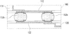
参照图1,其绘示依照本发明的一实施例的一种半导体封装结构100。此半导体封装结构100是由半导体元件110~140堆叠而成。 Referring to FIG. 1 , it illustrates a semiconductor package structure 100 according to an embodiment of the present invention. The semiconductor package structure 100 is formed by stacking semiconductor elements 110 - 140 . the
半导体元件110,在本实施例中,例如是芯片,具有一上表面110a及一下表面110b,该下表面110b具有多个焊垫112,及多个底下金属层114配置于焊垫112上。半导体元件110可通过配置于该底下金属层114上的第一凸块152a及第二凸块152b,接合至半导体元件120。该第一凸块152a配置于该半导体元件110的下表面110b的中间区域,该第二凸块152b配置于该半导体元件110的下表面110b的角落区域,该第二凸块152b围绕该第一凸块152而设置,且该第二凸块152b为一多重凸块结构160,亦即至少两个凸块相互电连接并提供相同的电性功能,可避免因元件翘曲,造成部分位于角落的凸块受到应力破坏而失效时,仍有与其电连接的其他凸块维持正常的功能。 In this embodiment, the
半导体元件120,在本实施例中,例如是中介基板,具有一上表面120a及一下表面120b,通过第三凸块154接合至线路基板130,配置于该第四表面120b的角落区域的第三凸块154,如上所述,可为一多重凸块结构。 The
线路基板130,具有一上表面130a及一下表面130b,通过第四凸块156接合至电路板140,配置于该下表面130b的角落区域的第四凸块156,如上所述,可为一多重凸块结构。 The circuit substrate 130 has an upper surface 130a and a lower surface 130b, and is bonded to the circuit board 140 through a fourth bump 156. The fourth bump 156 disposed in the corner area of the lower surface 130b, as mentioned above, can be a plurality of Heavy bump structure. the
多重凸块结构160,例如是由至少两个凸块152所构成,图1中的粗体线段代表通过此多重凸块结构160的导电路径172。通过位于半导体元件110上的导电路径172以及位于半导体元件120上的导电路径174来连接多重凸块结构160中的凸块152。 The
以下通过图2A-图2C来举例说明几种导电路径可能的设计。 2A-2C illustrate several possible designs of the conductive paths below. the
参照图2A,其更绘示图1的多重凸块结构160的局部放大图。所述导电路径172例如是位于半导体元件110中集成电路的一金属层118,而所述导电路径174例如是位于半导体元件120中集成电路的一金属层128。 Referring to FIG. 2A , it further shows a partially enlarged view of the
多重凸块结构经由半导体元件所提供的导电路径并不限于半导体元件中集成电路的一金属层。举凡半导体元件表层线路,皆可作为连接本申请的多重凸块结构的导电路径。 The conductive path provided by the multi-bump structure through the semiconductor device is not limited to a metal layer of the integrated circuit in the semiconductor device. For example, any surface circuit of the semiconductor element can be used as a conductive path connecting the multi-bump structure of the present application. the
如图2B所示,本实施例绘示该多重凸块结构160配置于该半导体元件110的底下金属层114上以及该半导体元件120的底下金属层124上,可经由该底下金属层114、124形成的导电路径,将所述多个第二凸块152b相互电连接。 As shown in FIG. 2B , the present embodiment shows that the
另一实施例,如图2C所示,绘示该多重凸块结构160配置于该半导体元件110的焊垫112上以及该半导体元件120的焊垫122,可经由相同焊垫形成的一导电路径,将所述多个第二凸块152b相互电连接。 Another embodiment, as shown in FIG. 2C, shows that the
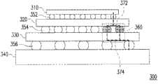
参考图3,其绘示依照本发明的另一实施例的一半导体封装结构300。此半导体封装结构300是由半导体元件310~320、线路基板330及电路板340堆叠而成,其中半导体元件310,例如是芯片,通过凸块352接合至半导体元件320,半导体元件320,例如是中介基板,通过凸块354接合至线路基板330,而线路基板330通过凸块356接合至电路板340。 Referring to FIG. 3 , it illustrates a
本实施例选择将半导体元件320与330的接面角落的凸块354形成多重凸块结构360。本实施例的多重凸块结构360例如是由两个凸块354所构成,而图3中的粗体线段代表通过此多重凸块结构360的导电路径。如图3所示,本实施例通过半导体元件320所提供的导电路径372以及半导体元件330所提供的导电路径374来连接多重凸块结构360中的凸块354。 In this embodiment, the
参考图4,其还绘示图3的多重凸块结构360的局部放大图。如图4所示,所述导电路径372例如是位于半导体元件320中集成电路的一金属层322。此外,导电路径374例如是位于线路基板330内部的线路332。多重凸块结构360的凸块354分别通过相应的导电通孔334连接到重布线路332。 Referring to FIG. 4 , it also shows a partially enlarged view of the
当然,本实施例也可以如图2B与2C所示,选择通过半导体元件的底下金属层以及焊垫来连接凸块354,此处不再赘述。 Of course, in this embodiment, as shown in FIGS. 2B and 2C , the
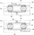
参考图5,其绘示依照本发明的又一实施例的一种半半导体封装结构500。此半导体封装结构500是由半导体元件510~520、线路基板530和电路板540堆叠而成,其中半导体元件510,例如是芯片,通过凸块552接合至半导体元件520,半导体元件520,例如是中介基板,通过凸块554接合至线路基板530,而线路基板530通过凸块556接合至电路板540。本实施例选择将半导体元件520与线路基板530的接面角落的凸块554形成多重凸块结构560。本实施例的多重凸块结构560例如是由两个凸块552所构成,而图5中的粗体线段代表通过此多重凸块结构560的导电路径。如图5所示,本实施例通过位于半导体元件520所提供的导电路径572以及位于半导体元件530所提供的导电路径574来连接多重凸块结构560中的凸块554。 Referring to FIG. 5 , it illustrates a semi-semiconductor package structure 500 according to yet another embodiment of the present invention. The semiconductor package structure 500 is formed by stacking semiconductor elements 510-520, a
图6还绘示图5的多重凸块结构560的局部放大图。如图6所示,所述导电路径572例如是位于半导体元件520中集成电路的一金属层522。此外, 导电路径574例如是位于半导体元件530内部的基板线路532。在此,半导体元件520为中介基板,且具有多个导电通孔(conductive via)524,以提供一垂直导电路径。多重凸块结构560的凸块554分别通过相应的导电通孔524向上连接到半导体元件520中集成电路的一金属层522。 FIG. 6 also shows a partially enlarged view of the
当然,本实施例也可以如图2B与2C所示,选择通过半导体元件的底下金属层以及焊垫来连接凸块554,此处不再赘述。 Of course, in this embodiment, as shown in FIGS. 2B and 2C , the
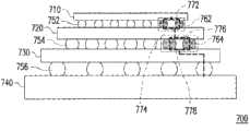
图7绘示依照本发明的再一实施例的一种半导体封装结构700。此半导体封装结构700是由半导体元件710~720、线路基板730和电路板740堆叠而成,其中半导体元件710,例如是芯片,通过凸块752接合至半导体元件720,半导体元件720,例如是中介基板,通过凸块754接合至线路基板730,而线路基板730通过凸块756接合至电路板740。 FIG. 7 illustrates a
本实施例在两处元件接面上分别形成多重凸块结构,包括选择将半导体元件710与720的接面角落的凸块752形成多重凸块结构760,以及,将半导体元件720与730的接面角落的凸块754形成多重凸块结构770。本实施例的多重凸块结构762例如是由两个凸块752所构成,多重凸块结构764例如是由两个凸块754所构成,而图7中的粗体线段代表通过多重凸块结构762与764的导电路径。如图7所示,本实施例通过位于半导体元件710上的导电路径772以及位于半导体元件720上的导电路径774来连接多重凸块结构762中的凸块752,并且,通过位于半导体元件720上的导电路径776以及位于半导体元件730上的导电路径778来连接多重凸块结构764中的凸块754。 In this embodiment, multiple bump structures are respectively formed on two component junctions, including selecting the
图8还绘示图7的多重凸块结构762与764的局部放大图。如图8所示,所述导电路径772例如是位于半导体元件710中集成电路的一金属层712。此外,导电路径774例如是位于半导体元件720中集成电路的一金属层722。此外,导电路径776例如是位于半导体元件720中集成电路的一金属层724。此外,导电路径778例如是位于半导体元件730内部的基板线路732。在此,半导体元件720为中介基板,具有导电通孔726,用以连接半导体元件720中集成电路的一金属层722与724。 FIG. 8 also shows a partially enlarged view of the
当然,本实施例也可以如图2B与2C所示,选择通过半导体元件的底下金属层以及焊垫来连接凸块752与754,此处不再赘述。 Certainly, in this embodiment, as shown in FIGS. 2B and 2C , the
综上所述,本申请通过在元件接面的角落上形成多重凸块结构可以增加 元件接面上的裂缝扩展路径。如此,当多重凸块结构中的部分凸块受到应力破坏而失效时,多重凸块结构中的其他凸块仍可维持正常的功能,以避免元件之间的电连接路径遭受应力破坏而失效,进而确保封装结构的可靠度。 In summary, the present application can increase the crack propagation path on the element junction by forming multiple bump structures on the corners of the element junction. In this way, when some of the bumps in the multi-bump structure fail due to stress damage, other bumps in the multi-bump structure can still maintain normal functions, so as to avoid the failure of the electrical connection path between components due to stress damage. Thus, the reliability of the packaging structure is ensured. the
此外,本申请提出的多重凸块结构可以应用于堆叠式封装的任两相邻的元件之间,且随着半导体封装结构的元件组成的不同,所选元件可能是芯片、中介基板、线路基板以及电路板等常见的半导体封装组成元件中的任两者。因此,上述多个实施例的封装结构仅是用来说明本发明的技术方案,并非用以限制此技术方案的应用范畴。本技术领域的技术人员当可依据实际状况对本申请提出的各个设计概念与变化进行组合、调整或省略,并且将其应用于各类封装结构的元件接面上,以达到类似的技术效果。 In addition, the multi-bump structure proposed in this application can be applied between any two adjacent components of the stacked package, and with the different components of the semiconductor package structure, the selected components may be chips, intermediary substrates, and circuit substrates. and any of the common components of semiconductor packages such as circuit boards. Therefore, the packaging structures of the above-mentioned multiple embodiments are only used to illustrate the technical solution of the present invention, and are not used to limit the application scope of the technical solution. Those skilled in the art can combine, adjust or omit various design concepts and changes proposed in this application according to the actual situation, and apply them to component junctions of various packaging structures to achieve similar technical effects. the
虽然结合以上实施例揭露了本发明,然而其并非用以限定本发明,任何所属技术领域中熟悉此技术者,在不脱离本发明的精神和范围内,可作些许的更动与润饰,故本发明的保护范围应以附上的权利要求所界定的为准。 Although the present invention has been disclosed in conjunction with the above embodiments, it is not intended to limit the present invention. Anyone skilled in the art can make some modifications and modifications without departing from the spirit and scope of the present invention. The scope of protection of the present invention should be defined by the appended claims. the
Claims (10)
Priority Applications (1)
| Application Number | Priority Date | Filing Date | Title |
|---|---|---|---|
| CN2011103056005ACN102361028A (en) | 2011-10-11 | 2011-10-11 | Semiconductor package structure with multi-bump structure |
Applications Claiming Priority (1)
| Application Number | Priority Date | Filing Date | Title |
|---|---|---|---|
| CN2011103056005ACN102361028A (en) | 2011-10-11 | 2011-10-11 | Semiconductor package structure with multi-bump structure |
Publications (1)
| Publication Number | Publication Date |
|---|---|
| CN102361028Atrue CN102361028A (en) | 2012-02-22 |
Family
ID=45586308
Family Applications (1)
| Application Number | Title | Priority Date | Filing Date |
|---|---|---|---|
| CN2011103056005APendingCN102361028A (en) | 2011-10-11 | 2011-10-11 | Semiconductor package structure with multi-bump structure |
Country Status (1)
| Country | Link |
|---|---|
| CN (1) | CN102361028A (en) |
Cited By (1)
| Publication number | Priority date | Publication date | Assignee | Title |
|---|---|---|---|---|
| US9508671B2 (en) | 2015-04-20 | 2016-11-29 | Advanced Semiconductor Engineering, Inc. | Semiconductor device and semiconductor package |
Citations (5)
| Publication number | Priority date | Publication date | Assignee | Title |
|---|---|---|---|---|
| US20080001296A1 (en)* | 2005-04-18 | 2008-01-03 | Chao-Chun Tu | Bond pad structures and semiconductor devices using the same |
| US20080157341A1 (en)* | 2006-12-29 | 2008-07-03 | Advanced Chip Engineering Technology Inc. | RF module package |
| CN101315922A (en)* | 2007-05-30 | 2008-12-03 | 力成科技股份有限公司 | Semiconductor packaging stacking device for preventing micro-contact welding spot fracture of semiconductor stacking |
| CN101355070A (en)* | 2007-07-24 | 2009-01-28 | 力成科技股份有限公司 | Stackable semiconductor packaging structure with multiple columns |
| CN102148166A (en)* | 2010-02-04 | 2011-08-10 | 力成科技股份有限公司 | Method and structure for filling multi-layer chip stacking gap |
- 2011
- 2011-10-11CNCN2011103056005Apatent/CN102361028A/enactivePending
Patent Citations (5)
| Publication number | Priority date | Publication date | Assignee | Title |
|---|---|---|---|---|
| US20080001296A1 (en)* | 2005-04-18 | 2008-01-03 | Chao-Chun Tu | Bond pad structures and semiconductor devices using the same |
| US20080157341A1 (en)* | 2006-12-29 | 2008-07-03 | Advanced Chip Engineering Technology Inc. | RF module package |
| CN101315922A (en)* | 2007-05-30 | 2008-12-03 | 力成科技股份有限公司 | Semiconductor packaging stacking device for preventing micro-contact welding spot fracture of semiconductor stacking |
| CN101355070A (en)* | 2007-07-24 | 2009-01-28 | 力成科技股份有限公司 | Stackable semiconductor packaging structure with multiple columns |
| CN102148166A (en)* | 2010-02-04 | 2011-08-10 | 力成科技股份有限公司 | Method and structure for filling multi-layer chip stacking gap |
Cited By (2)
| Publication number | Priority date | Publication date | Assignee | Title |
|---|---|---|---|---|
| US9508671B2 (en) | 2015-04-20 | 2016-11-29 | Advanced Semiconductor Engineering, Inc. | Semiconductor device and semiconductor package |
| US9768139B2 (en) | 2015-04-20 | 2017-09-19 | Advanced Semiconductor Engineering, Inc. | Semiconductor device and semiconductor package |
Similar Documents
| Publication | Publication Date | Title |
|---|---|---|
| US11469201B2 (en) | Semiconductor package and method for fabricating base for semiconductor package | |
| JP3581086B2 (en) | Semiconductor device | |
| JP5042668B2 (en) | Stacked package | |
| US9177899B2 (en) | Semiconductor package and method for fabricating base for semiconductor package | |
| TWI724189B (en) | Film product and film packages | |
| KR20130007049A (en) | Package on package using through silicon via technique | |
| US8502366B2 (en) | Semiconductor package | |
| US10043789B2 (en) | Semiconductor packages including an adhesive pattern | |
| KR20110091194A (en) | Laminated Semiconductor Packages | |
| CN111755392A (en) | semiconductor package | |
| US20140217573A1 (en) | Low cost and high performance flip chip package | |
| KR101321170B1 (en) | Package and Method for manufacturing the same | |
| KR101374144B1 (en) | Semiconductor device for preventing warpage | |
| KR101078744B1 (en) | Laminated Semiconductor Packages | |
| KR102723551B1 (en) | Semiconductor package | |
| TWI675459B (en) | Semiconductor structure and method for manufacturing the same | |
| CN102361028A (en) | Semiconductor package structure with multi-bump structure | |
| KR101099579B1 (en) | Stacked Chip Semiconductor Packages | |
| KR20110137059A (en) | Laminated Semiconductor Packages | |
| TWI435667B (en) | Print circuit board assembly | |
| KR20110091189A (en) | Laminated Semiconductor Packages | |
| JP3558070B2 (en) | Semiconductor device and manufacturing method thereof | |
| KR101169688B1 (en) | Semiconductor device and stacked semiconductor package | |
| JP2011119619A (en) | Semiconductor package | |
| JP6320681B2 (en) | Semiconductor device |
Legal Events
| Date | Code | Title | Description |
|---|---|---|---|
| C06 | Publication | ||
| PB01 | Publication | ||
| C10 | Entry into substantive examination | ||
| SE01 | Entry into force of request for substantive examination | ||
| C02 | Deemed withdrawal of patent application after publication (patent law 2001) | ||
| WD01 | Invention patent application deemed withdrawn after publication | Application publication date:20120222 |