CN102355136A - Control method and control circuit for controlling output current of converter - Google Patents
Control method and control circuit for controlling output current of converterDownload PDFInfo
- Publication number
- CN102355136A CN102355136ACN201110295481XACN201110295481ACN102355136ACN 102355136 ACN102355136 ACN 102355136ACN 201110295481X ACN201110295481X ACN 201110295481XACN 201110295481 ACN201110295481 ACN 201110295481ACN 102355136 ACN102355136 ACN 102355136A
- Authority
- CN
- China
- Prior art keywords
- signal
- current
- circuit
- control
- output
- Prior art date
- Legal status (The legal status is an assumption and is not a legal conclusion. Google has not performed a legal analysis and makes no representation as to the accuracy of the status listed.)
- Granted
Links
- 238000000034methodMethods0.000titleclaimsabstractdescription27
- 238000001514detection methodMethods0.000claimsabstractdescription109
- 238000005070samplingMethods0.000claimsabstractdescription10
- 238000004804windingMethods0.000claimsdescription14
- 230000008878couplingEffects0.000claimsdescription8
- 238000010168coupling processMethods0.000claimsdescription8
- 238000005859coupling reactionMethods0.000claimsdescription8
- 238000002955isolationMethods0.000claimsdescription7
- 238000001914filtrationMethods0.000claimsdescription2
- 230000000694effectsEffects0.000abstractdescription2
- 238000010586diagramMethods0.000description25
- 230000005284excitationEffects0.000description7
- 102100038817CDGSH iron-sulfur domain-containing protein 1Human genes0.000description6
- 101000883055Homo sapiens CDGSH iron-sulfur domain-containing protein 1Proteins0.000description6
- 239000003990capacitorSubstances0.000description5
- 230000003044adaptive effectEffects0.000description1
- 230000007547defectEffects0.000description1
- 238000010292electrical insulationMethods0.000description1
- 238000009413insulationMethods0.000description1
- 230000002452interceptive effectEffects0.000description1
- 238000012986modificationMethods0.000description1
- 230000004048modificationEffects0.000description1
Images


Landscapes
- Dc-Dc Converters (AREA)
Abstract
Translated fromChinese
Description
Translated fromChinese技术领域technical field
本发明涉电源电路,特别涉及一种控制变流器输出电流的控制方法及其控制电路。The invention relates to a power supply circuit, in particular to a control method and a control circuit for controlling the output current of a converter.
背景技术Background technique
在传统的在传统的小功率电源设备中,尤其是小功率开关电源,用于便携式设备的充电器,如手机充电器、笔记本电脑适配器、移动式设备的充电器,以及小功率LED照明的驱动电源,包括LED驱动器或者LED,其电源电路通常需要控制输出电流为恒定或者可调;传统的控制方式为对输出电流进行采样,然后用反馈电路控制电源电路中可控开关的导通时间或者频率进行调节。In traditional low-power power supply equipment, especially low-power switching power supplies, chargers for portable devices, such as mobile phone chargers, laptop adapters, mobile device chargers, and low-power LED lighting drivers Power supply, including LED driver or LED, its power supply circuit usually needs to control the output current to be constant or adjustable; the traditional control method is to sample the output current, and then use the feedback circuit to control the conduction time or frequency of the controllable switch in the power supply circuit Make adjustments.
在隔离型变流器中,通常使用变压器实现电气隔离;由于输出电流检测电路在主电路的输出端,但可控开关位于变压器的原边使得控制电路通常在主电路的输入端,这造成输出电流的反馈回路相应需要电气隔离;现有技术中一般选用的光耦隔离为:将输出电流反馈的误差信号经光耦输入原边上的控制电路,以控制原边上可控开关的工作状态。In an isolated converter, a transformer is usually used to achieve electrical isolation; since the output current detection circuit is at the output end of the main circuit, but the controllable switch is located at the primary side of the transformer, the control circuit is usually at the input end of the main circuit, which causes the output The current feedback loop needs electrical isolation accordingly; the optocoupler isolation generally selected in the prior art is: the error signal of the output current feedback is input into the control circuit on the primary side through the optocoupler to control the working state of the controllable switch on the primary side .
如图1所示的传统隔离型反激式变流器及其输出电流的控制电路,包括反馈电路W和集成电路A,反馈电路W位于反激电路的输出端,集成电路A位于反激电路的输入端;所述的反馈电路W采集电流输出端的电流信号Iload,将电流信号Iload与基准电压源U提供的基准电压信号Vref进行比较,产生一误差信号Vea,误差信号Vea经过光耦隔离传输到集成电路A,用来控制原边上可控开关Q的工作状态,实现反激电路输出电流的闭环控制。这种方法不仅线路复杂,因采集输出端的电流信号Iload导致增加电路损耗,而且光耦的存在对电气绝缘不利,容易产生漏电流,降低了电源电路的可靠性。As shown in Figure 1, the traditional isolated flyback converter and its output current control circuit include a feedback circuit W and an integrated circuit A, the feedback circuit W is located at the output end of the flyback circuit, and the integrated circuit A is located in the flyback circuit The input terminal; the feedback circuit W collects the current signal Iload of the current output terminal, compares the current signal Iload with the reference voltage signal Vref provided by the reference voltage source U, and generates an error signal Vea, and the error signal Vea is transmitted through optocoupler isolation To the integrated circuit A, which is used to control the working state of the controllable switch Q on the primary side, and realize the closed-loop control of the output current of the flyback circuit. This method not only has complex circuits, but also increases circuit loss due to the collection of the current signal Iload at the output end, and the existence of the optocoupler is not good for electrical insulation, which is prone to leakage current and reduces the reliability of the power supply circuit.
在非隔离型变流器中,尽管输入输出不需要电气隔离,但是由于采集输出端的电流信号与控制电路不共地,导致二者的电压参考点不一样,同样存在信号隔离的问题。如图2所示的BUCK-BOOST变流器及其输出电流的控制电路,BUCK-BOOST变流器即为非隔离型反激式变流器,为了方便驱动可控开关Q,一般将可控开关Q串联在输入端的地线上,这导致控制电路采集的输出端的电流信号Iload与控制电路的参考电位不一致。为了克服这种缺陷,实际操作中往往使用差分电路或者隔离的采样电路,如霍尔元件、电流互感器等,将电流信号Iload经过上述电路输入控制电路。但上述差分电路或采样电路通常价格较高,有不能适用高频场合等缺点,并且使用后存在与隔离型变流器相同的问题,如输出电流信号采样较困难、需要进行隔离等。In non-isolated converters, although the input and output do not need to be electrically isolated, because the current signal at the acquisition output terminal and the control circuit do not share the same ground, the voltage reference points of the two are different, and there is also the problem of signal isolation. The BUCK-BOOST converter and its output current control circuit are shown in Figure 2. The BUCK-BOOST converter is a non-isolated flyback converter. In order to facilitate the driving of the controllable switch Q, generally the controllable The switch Q is connected in series with the ground wire of the input end, which causes the current signal Iload of the output end collected by the control circuit to be inconsistent with the reference potential of the control circuit. In order to overcome this defect, differential circuits or isolated sampling circuits, such as Hall elements and current transformers, are often used in actual operation to input the current signal Iload into the control circuit through the above circuits. However, the above-mentioned differential circuit or sampling circuit is usually expensive, and has disadvantages such as not being suitable for high-frequency applications, and has the same problems as isolated converters after use, such as difficult sampling of output current signals and the need for isolation.
同样,如图3所示的一种非隔离型BUCK类变流器及其输出电流的控制电路,为了方便驱动可控开关Q,通常也将可控开关Q串联在输入端的地线上。显然,采集的输出端电流信号与控制电路的参考电位不一致,与BUCK-BOOST变流器输出电流的控制电路存在类似的问题。Similarly, for a non-isolated BUCK converter and its output current control circuit shown in Figure 3, in order to drive the controllable switch Q conveniently, the controllable switch Q is usually connected in series with the ground wire at the input end. Obviously, the collected output current signal is inconsistent with the reference potential of the control circuit, which is similar to the control circuit of the output current of the BUCK-BOOST converter.
除了上述输出电流的反馈控制电路外,不直接采样输出电流的控制电路也得到一定程度的使用,在隔离型变流器中,基于变压器输入端的电流信号进行输出电流的反馈控制,但这种控制电路一般仅适用于电流断续工作模式(DCM)和电流临界断续模式(CRM),不适用于电流连续模式(CCM),电路结构也非常复杂。In addition to the feedback control circuit of the output current mentioned above, the control circuit that does not directly sample the output current is also used to a certain extent. In the isolated converter, the feedback control of the output current is performed based on the current signal at the input terminal of the transformer, but this control The circuit is generally only suitable for discontinuous current mode (DCM) and critical discontinuous current mode (CRM), but not for continuous current mode (CCM), and the circuit structure is also very complicated.
公开号为CN101242143的中国专利于2008年8月13日公开了一种开关电路的自适应输出电流控制,该开关电路具有彼此电气绝缘的输入电路和输出电路;输出电流值可以基于输出电压,输出电路和表示相应于输出电压的输入电路中的电压的反射输出电压来确定;输入电路中的开关元件被控制来产生输出电流的确定值;存在下述问题:在CCM和DCM工作模式下的输出电流计算公式不一致,使得不同电流工作模式下的电路无法统一;DCM工作模式下的计算公式用到了开方计算,使得实现较为复杂。The Chinese patent with the publication number CN101242143 disclosed an adaptive output current control of a switch circuit on August 13, 2008. The switch circuit has an input circuit and an output circuit electrically insulated from each other; the output current value can be based on the output voltage, the output The circuit and the reflected output voltage representing the voltage in the input circuit corresponding to the output voltage are determined; the switching elements in the input circuit are controlled to produce a determined value of the output current; the following problems exist: the output in CCM and DCM operating modes The current calculation formulas are inconsistent, which makes the circuits in different current working modes unable to be unified; the calculation formulas in the DCM working mode use the square root calculation, which makes the implementation more complicated.
发明内容Contents of the invention
为解决如上所述的,在隔离型变流器中存在的输出电流控制电路复杂、损耗较大、绝缘性差和易产生漏电流等问题,在非隔离型变流器如BUCK-BOOST变流器和BUCK类变流器中存在的因输出电流控制电路与可控开关的输出电流参考电位不一致导致的技术难题,本发明提供了一种能够控制变流器输出电流的控制方法及其控制电路,在适用于DCM工作模式和CRM工作模式的同时也适用于CCM工作模式。In order to solve the problems of complex output current control circuit, large loss, poor insulation and easy leakage current in isolated converters as mentioned above, in non-isolated converters such as BUCK-BOOST converters In order to solve the technical problems caused by the inconsistency between the output current control circuit and the output current reference potential of the controllable switch in the BUCK type converter, the present invention provides a control method capable of controlling the output current of the converter and its control circuit, While being applicable to the DCM working mode and the CRM working mode, it is also applicable to the CCM working mode.
一种控制变流器输出电流的控制方法,包括以下步骤:A control method for controlling the output current of a converter, comprising the following steps:
(1)获取基准电压信号,并采集变流器中可控开关的电流信号和上一时刻的控制信号,以及变流器中的一电压信号;(1) Obtain the reference voltage signal, and collect the current signal of the controllable switch in the converter and the control signal at the previous moment, as well as a voltage signal in the converter;
(2)滤除所述的可控开关电流信号中的开关频率分量,得到平均电流信号;(2) filtering out the switching frequency component in the controllable switching current signal to obtain the average current signal;
(3)对所述的电压信号进行转换,得到电压指示信号,然后对所述的电压指示信号进行检测,得到二极管导通时间信号;(3) converting the voltage signal to obtain a voltage indication signal, and then detecting the voltage indication signal to obtain a diode conduction time signal;
(4)基于可控开关上一时刻的控制信号,得到可控开关导通时间信号;(4) Obtain the conduction time signal of the controllable switch based on the control signal of the controllable switch at the previous moment;
(5)基于所述的平均电流信号、二极管导通时间信号和可控开关导通时间信号,计算得到输出电流信号;将所述的输出电流信号与所述的基准电压信号进行比较,得到误差信号;(5) Calculate the output current signal based on the average current signal, the diode conduction time signal and the controllable switch conduction time signal; compare the output current signal with the reference voltage signal to obtain the error Signal;
(6)将所述的误差信号进行调制得到可控开关当前时刻的控制信号,以控制变流器中可控开关的导通或关断;所述的调制以PWM调制为最佳。(6) The error signal is modulated to obtain the control signal of the controllable switch at the current moment, so as to control the turn-on or turn-off of the controllable switch in the converter; the modulation is preferably PWM modulation.
所述的步骤(1)中,可以对变流器的交流信号进行切相角控制,并经调制获取基准电压信号。In the step (1), the phase angle control of the AC signal of the converter can be performed, and the reference voltage signal can be obtained through modulation.
所述的步骤(3)中,对电压指示信号进行检测的过程为:先对所述的电压指示信号进行过零检测,得到零电流检测信号;然后对所述的零电流检测信号进行脉宽检测,得到二极管导通时间信号。In the step (3), the process of detecting the voltage indication signal is as follows: first, the zero-crossing detection is performed on the voltage indication signal to obtain a zero-current detection signal; then, the pulse width of the zero-current detection signal is Detect and get the diode conduction time signal.
所述的步骤(4)中,对可控开关上一时刻的控制信号进行脉宽检测,得到可控开关导通时间信号。In the step (4), pulse width detection is performed on the control signal of the controllable switch at a previous moment to obtain a conduction time signal of the controllable switch.
所述的步骤(5)中,基于平均电流信号、二极管导通时间信号和可控开关导通时间信号,计算输出电流信号的公式为:In the step (5), based on the average current signal, the diode conduction time signal and the controllable switch conduction time signal, the formula for calculating the output current signal is:
在反激式变流器中为:In a flyback converter it is:
Io=Iavg*Ton_s/Ton_p;Io=Iavg*Ton_s/Ton_p;
在BUCK类变流器中为:In the BUCK type converter is:
Io=Iavg*(Ton_s+Ton_p)/Ton_p;Io=Iavg*(Ton_s+Ton_p)/Ton_p;
其中,Io为输出电流信号,Iavg为平均电流信号,Ton_s为二极管导通时间信号,Ton_p为可控开关导通时间信号。Among them, Io is the output current signal, Iavg is the average current signal, Ton_s is the diode conduction time signal, and Ton_p is the controllable switch conduction time signal.
一种控制变流器输出电流的控制电路,包括:A control circuit for controlling the output current of a converter, comprising:
低通滤波器,用于接收变流器中可控开关的电流信号,并输出平均电流信号;所述的低通滤波器可以为RC滤波器;A low-pass filter is used to receive the current signal of the controllable switch in the converter and output the average current signal; the low-pass filter can be an RC filter;
电压采样电路,用于采集变流器中的电压信号,并输出电压指示信号;所述的电压采样电路:在隔离型变流器,如隔离型反激式变流器中,为变流器中反激变压器的辅助绕组或微分电路;在非隔离型变流器,如BUCK-BOOST变流器和非隔离型BUCK类变流器中,为变流器中电感的耦合绕组;The voltage sampling circuit is used to collect the voltage signal in the converter and output the voltage indication signal; the voltage sampling circuit is: in an isolated converter, such as an isolated flyback converter, it is a converter The auxiliary winding or differential circuit of the flyback transformer; in non-isolated converters, such as BUCK-BOOST converters and non-isolated BUCK converters, it is the coupling winding of the inductance in the converter;
二极管导通时间检测电路,用于接收所述的电压指示信号,并输出二极管导通时间信号;所述的二极管导通时间检测电路,包括:The diode conduction time detection circuit is used to receive the voltage indication signal and output the diode conduction time signal; the diode conduction time detection circuit includes:
过零检测电路,用于接收所述的电压指示信号,输出零电流检测信号;A zero-crossing detection circuit, configured to receive the voltage indication signal and output a zero-current detection signal;
脉宽检测电路,用于接收所述的零电流检测信号,输出二极管导通时间信号;A pulse width detection circuit for receiving the zero current detection signal and outputting a diode conduction time signal;
可控开关导通时间检测电路,用于接收可控开关上一时刻的控制信号,并输出可控开关导通时间信号;The conduction time detection circuit of the controllable switch is used to receive the control signal of the previous moment of the controllable switch and output the conduction time signal of the controllable switch;
运算电路,用于接收所述的平均电流信号、二极管导通时间信号和可控开关导通时间信号,并产生输出电流信号;所述的运算电路可以为乘法器;An operation circuit, used to receive the average current signal, the diode conduction time signal and the controllable switch conduction time signal, and generate an output current signal; the operation circuit may be a multiplier;
基准电压源,用于提供基准电压信号;A reference voltage source, configured to provide a reference voltage signal;
误差补偿电路,用于接收所述的基准电压信号以及所述的输出电流信号,并输出误差信号;an error compensation circuit, configured to receive the reference voltage signal and the output current signal, and output an error signal;
调制电路,用于接收所述的误差信号,并输出可控开关当前时刻的控制信号至可控开关的控制端;所述的调制电路可以为PWM调制电路。The modulation circuit is used to receive the error signal, and output the control signal of the controllable switch to the control terminal of the controllable switch; the modulation circuit can be a PWM modulation circuit.
本发明通过采集可控开关的电流信号、变流器中的电压信号和可控开关上一时刻的控制信号,并获取基准电压源提供的基准电压信号,经计算、比较、检测和调制等处理,得出平均电流信号、二极管导通时间信号和可控开关导通时间信号,产生控制可控开关导通或关断的可控开关当前时刻的控制信号,以达到控制变流器输出电流的效果,能够应用于各种控制方式,如变频率控制(VF,variable frequency)、定频控制方式(CF,constantfrequency);并且,本发明基于可控开关输出端的信号和变流器中的电压信号即可得到输出电流的信息,实现输出电流的间接控制,减少对变流器的电流采样,不但简化了电路结构、降低了电路损耗,也节约了电路组成的成本费用。The present invention collects the current signal of the controllable switch, the voltage signal in the converter and the control signal of the previous moment of the controllable switch, and obtains the reference voltage signal provided by the reference voltage source, and processes such as calculation, comparison, detection and modulation , get the average current signal, the diode conduction time signal and the controllable switch conduction time signal, and generate the control signal of the controllable switch that controls the controllable switch to be turned on or off at the current moment, so as to control the output current of the converter effect, can be applied to various control modes, such as variable frequency control (VF, variable frequency), fixed frequency control mode (CF, constant frequency); and, the present invention is based on the signal of the output terminal of the controllable switch and the voltage signal in the converter The information of the output current can be obtained, the indirect control of the output current can be realized, and the current sampling of the converter can be reduced, which not only simplifies the circuit structure, reduces the circuit loss, but also saves the cost of the circuit composition.
附图说明Description of drawings
图1为一种隔离型反激式变流器及现有技术中一种控制其输出电流的控制电路的结构示意图。FIG. 1 is a structural schematic diagram of an isolated flyback converter and a control circuit for controlling its output current in the prior art.
图2为一种BUCK-BOOST变流器及现有技术中一种控制其输出电流的控制电路的结构示意图。FIG. 2 is a structural schematic diagram of a BUCK-BOOST converter and a control circuit for controlling its output current in the prior art.
图3为一种非隔离型BUCK类变流器及现有技术中一种控制其输出电流的控制电路的结构示意图。FIG. 3 is a structural schematic diagram of a non-isolated BUCK converter and a control circuit for controlling its output current in the prior art.
图4为本发明一种控制变流器输出电流的方法的流程示意图。FIG. 4 is a schematic flowchart of a method for controlling the output current of a converter according to the present invention.
图5为图1所示的隔离型反激式变流器及本发明控制其输出电流的一种控制电路的结构示意图。FIG. 5 is a structural schematic diagram of the isolated flyback converter shown in FIG. 1 and a control circuit for controlling its output current according to the present invention.
图6为图5中控制电路A的内部结构方框图。FIG. 6 is a block diagram of the internal structure of the control circuit A in FIG. 5 .
图7为图6中RC滤波器A1的电路结构示意图。FIG. 7 is a schematic diagram of the circuit structure of the RC filter A1 in FIG. 6 .
图8为图5电路的工作波形图。FIG. 8 is a working waveform diagram of the circuit in FIG. 5 .
图9为图6中二极管导通时间检测电路A2的一种结构示意图。FIG. 9 is a schematic structural diagram of the diode conduction time detection circuit A2 in FIG. 6 .
图10为图9中二极管导通时间检测电路A2去掉RS触发器F的结构示意图。FIG. 10 is a schematic structural diagram of the diode conduction time detection circuit A2 in FIG. 9 without the RS flip-flop F.
图11为图6中可控开关导通时间检测电路A3的一种结构示意图。FIG. 11 is a schematic structural diagram of the turn-on time detection circuit A3 of the controllable switch in FIG. 6 .
图12为图6中误差补偿电路A5的一种结构示意图。FIG. 12 is a schematic structural diagram of the error compensation circuit A5 in FIG. 6 .
图13为图6中脉宽调制电路A6的一种结构示意图。FIG. 13 is a schematic structural diagram of the pulse width modulation circuit A6 in FIG. 6 .
图14为图6中以数字化方式实现二极管导通时间检测电路A2的一种结构示意图。FIG. 14 is a schematic structural diagram of a digitally implemented diode conduction time detection circuit A2 in FIG. 6 .
图15为图14中二极管导通时间检测电路A2去掉RS触发器F的结构示意图。FIG. 15 is a schematic structural diagram of the diode conduction time detection circuit A2 in FIG. 14 without the RS flip-flop F.
图16为图6中以数字化方式实现可控开关导通时间检测电路A3的一种结构示意图。FIG. 16 is a schematic structural diagram of a controllable switch on-time detection circuit A3 implemented digitally in FIG. 6 .
图17为图1所示的隔离型反激式变流器及本发明控制其输出电流的一种带微分电路的控制电路的结构示意图。FIG. 17 is a structural schematic diagram of the isolated flyback converter shown in FIG. 1 and a control circuit with a differential circuit for controlling its output current according to the present invention.
图18为图17所示电路的工作波形图。FIG. 18 is a working waveform diagram of the circuit shown in FIG. 17 .
图19为图2所示的BUCK-BOOST变流器及本发明控制其输出电流的一种控制电路的结构示意图。FIG. 19 is a structural schematic diagram of the BUCK-BOOST converter shown in FIG. 2 and a control circuit for controlling its output current according to the present invention.
图20为图3所示的非隔离型BUCK类变流器及本发明控制其输出电流的一种控制电路的结构示意图。FIG. 20 is a structural schematic diagram of the non-isolated BUCK converter shown in FIG. 3 and a control circuit for controlling its output current according to the present invention.
图21为图20中控制电路A的内部结构方框图。FIG. 21 is a block diagram of the internal structure of the control circuit A in FIG. 20 .
图22为图20所示电路的工作波形图。FIG. 22 is a working waveform diagram of the circuit shown in FIG. 20 .
图23为一种含TRIAC调光电路的隔离型变流器及本发明控制其输出电流的一种控制电路的结构示意图。FIG. 23 is a structural schematic diagram of an isolated converter including a TRIAC dimming circuit and a control circuit for controlling its output current according to the present invention.
图24为基准电压源U的一种结构示意图。FIG. 24 is a schematic structural diagram of the reference voltage source U.
图25为TRIAC调光电路的输入电压波形图。FIG. 25 is a waveform diagram of the input voltage of the TRIAC dimming circuit.
图26为PWM调制的一种电路实施示意图。FIG. 26 is a schematic diagram of a circuit implementation of PWM modulation.
具体实施方式Detailed ways
下面结合附图详细介绍本发明的具体实施方式,然而,应当清楚,本发明的原理对任何可控开关电流与输出电流有对应关系的电源电路均适用。The specific implementation of the present invention will be described in detail below with reference to the accompanying drawings. However, it should be clear that the principle of the present invention is applicable to any power supply circuit that has a corresponding relationship between controllable switch current and output current.
如图4所示的一种控制变流器输出电流的控制方法,包括以下步骤:A control method for controlling the output current of a converter as shown in FIG. 4 includes the following steps:
S1采集变流器中可控开关的电流信号、变流器中的电压信号、可控开关上一时刻的控制信号,并获取基准电压信号;S1 collects the current signal of the controllable switch in the converter, the voltage signal in the converter, the control signal of the controllable switch at the previous moment, and obtains the reference voltage signal;
S2滤除可控开关电流信号中的开关频率分量,得到平均电流信号;S2 filters out the switching frequency component in the controllable switch current signal to obtain the average current signal;
S3对电压信号进行转换,得到电压指示信号;对电压指示信号进行检测,得到二极管导通时间信号;S3 converts the voltage signal to obtain a voltage indication signal; detects the voltage indication signal to obtain a diode conduction time signal;
S3中,对电压指示信号进行检测包括如下步骤:In S3, detecting the voltage indication signal includes the following steps:
S31对电压指示信号进行过零检测,得到零电流检测信号;S31 performs zero-crossing detection on the voltage indication signal to obtain a zero-current detection signal;
S32对零电流检测信号进行脉宽检测,得到二极管导通时间信号;S32 detects the pulse width of the zero current detection signal to obtain a diode conduction time signal;
S4对可控开关上一时刻的控制信号进行脉宽检测,得到可控开关导通时间信号;S4 detects the pulse width of the control signal of the controllable switch at the previous moment, and obtains the conduction time signal of the controllable switch;
S5中,S51基于平均电流信号、二极管导通时间信号和可控开关导通时间信号,计算得到输出电流信号;In S5, S51 calculates the output current signal based on the average current signal, the diode conduction time signal and the controllable switch conduction time signal;
其中,计算输出电流信号的公式为:Among them, the formula for calculating the output current signal is:
S511在反激式变流器中为:S511 in the flyback converter is:
Io=Iavg*Ton_s/Ton_p;Io=Iavg*Ton_s/Ton_p;
S512在BUCK类变流器中为:S512 in the BUCK converter is:
Io=Iavg*(Ton_s+Ton_p)/Ton_p;Io=Iavg*(Ton_s+Ton_p)/Ton_p;
其中,Io为输出电流信号,Iavg为平均电流信号,Ton_s为二极管导通时间信号,Ton_p为可控开关导通时间信号;Among them, Io is the output current signal, Iavg is the average current signal, Ton_s is the diode conduction time signal, Ton_p is the controllable switch conduction time signal;
S52将输出电流信号与基准电压信号进行比较,得到误差信号;S52 compares the output current signal with the reference voltage signal to obtain an error signal;
S6对误差信号进行PWM调制,得到可控开关当前时刻的控制信号,以可控开关当前时刻的控制信号控制变流器中可控开关的导通或关断,从而控制产生变流器输出电流为一确定值。S6 performs PWM modulation on the error signal to obtain the control signal of the controllable switch at the current moment, and uses the control signal of the controllable switch at the current moment to control the turn-on or turn-off of the controllable switch in the converter, thereby controlling the generation of the output current of the converter is a certain value.
实施例1:Example 1:
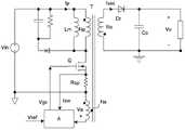
如图5所示的一种控制隔离型反激式变流器输出电流的控制电路,包括:集成电路A、基准电压源U、反激式变流器中的反激变压器T、接入反激变压器T原边的可控开关Q和反激变压器T的辅助绕组Na;As shown in Figure 5, a control circuit for controlling the output current of an isolated flyback converter includes: an integrated circuit A, a reference voltage source U, a flyback transformer T in the flyback converter, and an access flyback The controllable switch Q on the primary side of the excitation transformer T and the auxiliary winding Na of the flyback transformer T;
辅助绕组Na采集反激式变流器中变压器上的电压信号,输出电压指示信号Va;The auxiliary winding Na collects the voltage signal on the transformer in the flyback converter, and outputs the voltage indicating signal Va;
集成电路A的第一输入端与可控开关Q的输出端相连,并接收可控开关Q的电流信号Isw;The first input end of the integrated circuit A is connected to the output end of the controllable switch Q, and receives the current signal Isw of the controllable switch Q;
集成电路A的第二输入端与辅助绕组Na的正端相连,并接收电压指示信号Va;The second input terminal of the integrated circuit A is connected to the positive terminal of the auxiliary winding Na, and receives the voltage indication signal Va;
集成电路A的第三输入端接收基准电压源U提供的基准电压信号Vref;基准电压信号Vref也可以选择在集成电路A的内部实现;The third input terminal of the integrated circuit A receives the reference voltage signal Vref provided by the reference voltage source U; the reference voltage signal Vref can also be implemented inside the integrated circuit A;
集成电路A的输出端与可控开关Q的控制端相连,输出可控开关当前时刻的控制信号Vgs。The output terminal of the integrated circuit A is connected to the control terminal of the controllable switch Q, and outputs the control signal Vgs of the controllable switch at the current moment.
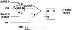
如图6所示,集成电路A包括:As shown in Figure 6, integrated circuit A includes:
RC滤波器A1、二极管导通时间检测电路A2、可控开关导通时间检测电路A3、乘法器A4、误差补偿电路A5和脉宽调制电路A6:RC filter A1, diode conduction time detection circuit A2, controllable switch conduction time detection circuit A3, multiplier A4, error compensation circuit A5 and pulse width modulation circuit A6:
RC滤波器A1的输入端11为集成电路A的第一输入端,接收可控开关的电流信号Isw;RC滤波器A1的输出端1与乘法器A4的第一输入端41相连并输出平均电流信号Iavg;The
二极管导通时间检测电路A2输入端21为集成电路A的第二输入端,接收电压指示信号Va;二极管导通时间检测电路A2的输出端2与乘法器A4的第二输入端42相连并输出二极管导通时间信号Ton_s;The
可控开关导通时间检测电路A3的输入端31接收可控开关上一时刻的控制信号Vgs,可控开关导通时间检测电路A3的输出端3与乘法器A4的第三输入端43相连并输出可控开关导通时间信号Ton_p;The
乘法器A4的第一输入端41接收平均电流信号Iavg,第二输入端42接收二极管导通时间信号Ton_s,第三输入端43接收输出端可控开关导通时间信号Ton_p;乘法器A4的输出端4与误差补偿电路A5的第一输入端51相连并输出输出电流信号Io;乘法器A4内部实现的计算公式为:Io=Iavg*Ton_s/Ton_p;The
误差补偿电路A5的第一输入端51接收输出电流信号Io,第二输入端52为集成电路A的第三输入端,并接收基准电压信号Vref;误差补偿电路A5的输出端5与脉宽调制电路A6的输入端61相连并输出误差信号Vea;The
脉宽调制电路A6的输入端61接收误差信号Vea,输出端6为集成电路A的输出端,输出可控开关当前时刻控制信号Vgs。The
如图7所示的RC滤波器A1,电阻R与电容C的串联端为RC滤波器A1的输出端1,电阻R的另一端为RC滤波器A1的输入端11。In the RC filter A1 shown in FIG. 7 , the series terminal of the resistor R and the capacitor C is the
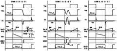
如图9所示的二极管导通时间检测电路A2,包括过零检测电路A21和脉宽检测电路A22;过零检测电路A21中的比较器B的正端为二极管导通时间检测电路A2的输入端21,接收电压指示信号Va,比较器B的输出端输出零电流信号ZCD1,零电流信号ZCD1经过RS触发器F,在与门G的输出端输出零电流检测信号ZCD;脉宽检测电路A22的输出端为二极管导通时间检测电路A2的输出端2,脉宽检测电路A22的输入端接收零电流检测信号ZCD,在输出端输出二极管导通时间信号Ton_s;The diode conduction time detection circuit A2 as shown in Figure 9 includes a zero-crossing detection circuit A21 and a pulse width detection circuit A22; the positive terminal of the comparator B in the zero-crossing detection circuit A21 is the input of the diode conduction time detection circuit A2 The terminal 21 receives the voltage indication signal Va, and the output terminal of the comparator B outputs the zero current signal ZCD1, the zero current signal ZCD1 passes through the RS flip-flop F, and outputs the zero current detection signal ZCD at the output terminal of the AND gate G; the pulse width detection circuit A22 The output terminal of is the
结合图8可知,在电流工作模式为DCM模式下,如果电流断续时间比较长,比较器B的输出端输出的零电流信号ZCD1在二极管电流为零期间会输出一个窄脉冲It,这可能影响二极管导通时间检测电路A2正常检测二极管导通时间信号Ton_s;在本实施例中,如图9所示,二极管导通时间检测电路A2中的过零检测电路A21包括的RS触发器F实现了本控制电路可以同时适用于CRM、DCM和CCM三种电流工作模式;在DCM模式下,RS触发器F的S端接收可控开关内部提供的可控开关上一时刻的控制信号Vgs,实现在可控开关Q关断时,可控开关控制信号Vgs为下降沿,只有第一个下降沿触发有效,以屏蔽后面的脉冲;而在CRM和CCM模式下,不存在上述问题,可以选择去掉RS触发器F,如图10所示的去掉RS触发器F的二极管导通时间检测电路A2,过零检测电路A21中的比较器B的正端为二极管导通时间检测电路A2的输入端21,接收电压指示信号Va,比较器B的输出端输出的为零电流检测信号ZCD;脉宽检测电路A22的输出端为二极管导通时间检测电路A2的输出端2,脉宽检测电路A22的输入端接收零电流检测信号ZCD,并在输出端输出二极管导通时间信号Ton_s。Combining with Figure 8, it can be seen that when the current working mode is DCM mode, if the current discontinuity time is relatively long, the zero current signal ZCD1 output by the output terminal of comparator B will output a narrow pulse It during the period when the diode current is zero, which may affect The diode conduction time detection circuit A2 normally detects the diode conduction time signal Ton_s; in this embodiment, as shown in Figure 9, the RS flip-flop F included in the zero-crossing detection circuit A21 in the diode conduction time detection circuit A2 realizes This control circuit can be applied to three current working modes of CRM, DCM and CCM at the same time; in the DCM mode, the S terminal of the RS flip-flop F receives the control signal Vgs of the controllable switch at the previous moment provided by the controllable switch, and realizes When the controllable switch Q is turned off, the controllable switch control signal Vgs is a falling edge, and only the first falling edge trigger is valid to shield the subsequent pulses; in the CRM and CCM modes, the above problems do not exist, you can choose to remove RS Flip-flop F, as shown in FIG. 10 , remove the diode conduction time detection circuit A2 of the RS trigger F, and the positive terminal of the comparator B in the zero-crossing detection circuit A21 is the input terminal 21 of the diode conduction time detection circuit A2, Receive the voltage indication signal Va, the output terminal of the comparator B outputs the zero current detection signal ZCD; the output terminal of the pulse width detection circuit A22 is the output terminal 2 of the diode conduction time detection circuit A2, and the input terminal of the pulse width detection circuit A22 Receive the zero current detection signal ZCD, and output the diode conduction time signal Ton_s at the output terminal.
如图11所示的一种可控开关导通时间检测电路A3,为一种脉宽检测电路,脉宽检测电路的输入端为可控开关导通时间检测电路A3的输入端31,脉宽调制电路的输出端为可控开关导通时间检测电路A3的输出端3。A controllable switch conduction time detection circuit A3 as shown in Figure 11 is a pulse width detection circuit, the input terminal of the pulse width detection circuit is the
如图12所示的一种误差补偿电路A5,包括比较器B1,其中比较器B1的负端为误差补偿电路A5的第一输入端51,比较器B1的正端为误差补偿电路A5的第二输入端52,比较器B1的输出端为为误差补偿电路A5的输出端5。An error compensation circuit A5 as shown in FIG. 12 includes a comparator B1, wherein the negative terminal of the comparator B1 is the
如图13所示的一种脉宽调制电路A6,包括比较器B2和RS触发器F1,比较器B2的负端为脉宽调制电路A6的输入端61;RS触发器F1的R端连接比较器B2的输出端,RS触发器F1的Q端为脉宽调制电路A6的输出端6。A pulse width modulation circuit A6 as shown in Figure 13 includes a comparator B2 and an RS flip-flop F1, the negative end of the comparator B2 is the
本实施例控制变流器输出电流的控制方法,包括以下步骤:The control method for controlling the output current of the converter in this embodiment includes the following steps:
(1)采集变流器中可控开关Q的电流信号Isw、变流器中变压器的电压信号、可控开关上一时刻的控制信号Vgs,并获取基准电压信号Vref;(1) Collect the current signal Isw of the controllable switch Q in the converter, the voltage signal of the transformer in the converter, the control signal Vgs of the controllable switch at the previous moment, and obtain the reference voltage signal Vref;
(2)滤除可控开关电流信号Isw中的开关频率分量,得到平均电流信号Iavg;(2) Filter out the switching frequency component in the controllable switching current signal Isw to obtain the average current signal Iavg;
(3)对电压信号进行转换,得到电压指示信号Va;对电压指示信号Va进行检测,得到二极管导通时间信号Ton_s;(3) Convert the voltage signal to obtain the voltage indication signal Va; detect the voltage indication signal Va to obtain the diode conduction time signal Ton_s;
对电压指示信号Va进行检测包括如下步骤:Detecting the voltage indication signal Va includes the following steps:
(a)对电压指示信号Va进行过零检测,得到零电流检测信号ZCD;(a) Perform zero-crossing detection on the voltage indication signal Va to obtain a zero-current detection signal ZCD;
(b)对零电流检测信号ZCD进行脉宽检测,得到二极管导通时间信号Ton_s;(b) Perform pulse width detection on the zero current detection signal ZCD to obtain the diode conduction time signal Ton_s;
在二极管导通时间检测中,可采用模拟的方法实现,在本实施例中,利用零电流检测信号ZCD控制一恒流源,恒流源在零电流检测信号ZCD有效期间持续对一电容充电,电容的电压与脉冲宽度成正比,利用此电压值,得到二极管导通时间信号Ton_s;In the detection of the conduction time of the diode, it can be realized by an analog method. In this embodiment, the zero current detection signal ZCD is used to control a constant current source, and the constant current source continues to charge a capacitor during the effective period of the zero current detection signal ZCD. The voltage of the capacitor is proportional to the pulse width. Using this voltage value, the diode conduction time signal Ton_s is obtained;
更为简单的方式是将ZCD信号经过一个低通滤波器(可以采用同图7所述的RC滤波器的电路结构形式),得到其平均值,该平均值与ZCD信号的脉宽成正比,也体现了二极管的导通时间。A simpler way is to pass the ZCD signal through a low-pass filter (the same circuit structure of the RC filter described in Figure 7 can be used) to obtain its average value, which is proportional to the pulse width of the ZCD signal, It also reflects the conduction time of the diode.
(4)对可控开关上一时刻的控制信号Vgs进行脉宽检测,得到可控开关导通时间信号Ton_p;(4) Perform pulse width detection on the control signal Vgs of the controllable switch at the previous moment, and obtain the conduction time signal Ton_p of the controllable switch;
在可控开关导通时间检测中,可采用模拟的方法实现,在本实施例中,利用可控开关上一时刻的控制信号Vgs控制一恒流源,恒流源在可控开关上一时刻的控制信号Vgs有效期间持续对一电容充电,电容的电压与脉冲宽度成正比,利用此电压值,得到可控开关导通时间信号Ton_p;In the detection of the turn-on time of the controllable switch, an analog method can be used to realize it. In this embodiment, a constant current source is controlled by the control signal Vgs at the previous moment of the controllable switch. During the effective period of the control signal Vgs, a capacitor is continuously charged, and the voltage of the capacitor is proportional to the pulse width. Using this voltage value, the controllable switch conduction time signal Ton_p is obtained;
更为简单的方式是将Vgs信号经过一个低通滤波器(可以采用同图7所述的RC滤波器的电路结构形式),得到其平均值,该平均值与Vgs信号的脉宽成正比,也体现了开关管的导通时间。A simpler way is to pass the Vgs signal through a low-pass filter (the same circuit structure of the RC filter as shown in Figure 7 can be used) to obtain its average value, which is proportional to the pulse width of the Vgs signal, It also reflects the conduction time of the switch tube.
(5)基于平均电流信号Iavg、二极管导通时间信号Ton_s和可控开关导通时间信号Ton_p,计算得到输出电流信号Io;(5) Calculate the output current signal Io based on the average current signal Iavg, the diode conduction time signal Ton_s and the controllable switch conduction time signal Ton_p;
其中,计算公式为:Among them, the calculation formula is:
Io=Iavg*Ton_s/Ton_p;Io=Iavg*Ton_s/Ton_p;
将输出电流信号Io与基准电压信号Vref进行比较,得到误差信号Vea;Comparing the output current signal Io with the reference voltage signal Vref to obtain the error signal Vea;
(6)将误差信号Vea进行PWM调制得到可控开关Q当前时刻的控制信号Vgs,以控制变流器中可控开关Q的导通或关断,从而控制产生变流器输出电流的确定值。(6) Perform PWM modulation on the error signal Vea to obtain the control signal Vgs of the controllable switch Q at the current moment, so as to control the turn-on or turn-off of the controllable switch Q in the converter, so as to control the definite value of the output current of the converter .
实施例2:Example 2:
本实施例中的一种控制隔离型反激式变流器输出电流的控制电路的其他结构与实施例1相同,与实施例1不同的是,实现脉宽检测采用了数字化的方式:The other structure of the control circuit for controlling the output current of the isolated flyback converter in this embodiment is the same as that of
集成电路A中的二极管导通时间检测电路A2包括过零检测电路A21与计数器A22,如图14所示的一种二极管导通时间检测电路A2,过零检测电路A21中的比较器B的正端为二极管导通时间检测电路A2的输入端21,接收电压指示信号Va,比较器B的输出端输出零电流信号ZCD1,零电流信号ZCD1经过RS触发器F,在与门G的输出端输出零电流检测信号ZCD;计数器A22的输出端为二极管导通时间检测电路A2的输出端2,计数器A22的输入端接收零电流检测信号ZCD,在输出端输出二极管导通时间信号Ton_s;The diode conduction time detection circuit A2 in the integrated circuit A includes a zero-crossing detection circuit A21 and a counter A22, a diode conduction time detection circuit A2 as shown in FIG. The terminal is the
与实施例1相同,二极管导通时间检测电路A2中的过零检测电路A21包括的RS触发器F实现了本控制电路可以同时适用于CRM、DCM和CCM三种电流工作模式;而在CRM和CCM的工作模式下,过零检测电路A21可以选择去掉RS触发器F,二极管导通时间检测电路A2此时的电路结构则如图15所示;Same as
集成电路A中的可控开关导通时间检测电路A3,如图16所示,为一计数器,计数器的输入端为可控开关导通时间检测电路A3的输入端31,接收可控开关上一时刻的控制信号Vgs;计数器的输出端为可控开关导通时间检测电路A3的输出端3,输出可控开关导通时间信号Ton_p。The on-time detection circuit A3 of the controllable switch in the integrated circuit A, as shown in FIG. Time control signal Vgs; the output terminal of the counter is the
本实施例控制变流器输出电流的控制方法,包括以下步骤:The control method for controlling the output current of the converter in this embodiment includes the following steps:
(1)获取基准电压信号Vref,并采集变流器中可控开关Q的电流信号Isw、变流器中变压器的电压信号、可控开关上一时刻的控制信号Vgs;(1) Obtain the reference voltage signal Vref, and collect the current signal Isw of the controllable switch Q in the converter, the voltage signal of the transformer in the converter, and the control signal Vgs of the controllable switch at the previous moment;
(2)滤除可控开关电流信号Isw中的开关频率分量,得到平均电流信号Iavg;(2) Filter out the switching frequency component in the controllable switching current signal Isw to obtain the average current signal Iavg;
(3)对电压信号进行转换,得到电压指示信号Va;对电压指示信号Va进行检测,得到二极管导通时间信号Ton_s;(3) Convert the voltage signal to obtain the voltage indication signal Va; detect the voltage indication signal Va to obtain the diode conduction time signal Ton_s;
对电压指示信号Va进行检测包括如下步骤:Detecting the voltage indication signal Va includes the following steps:
(a)对电压指示信号Va进行过零检测,得到零电流检测信号ZCD;(a) Perform zero-crossing detection on the voltage indication signal Va to obtain a zero-current detection signal ZCD;
(b)对零电流检测信号ZCD进行脉宽检测,得到二极管导通时间信号Ton_s;在本实施例中,利用计数测试零电流检测信号ZCD的脉冲宽度,得到二极管导通时间信号Ton_s。(b) Perform pulse width detection on the zero current detection signal ZCD to obtain the diode conduction time signal Ton_s; in this embodiment, the pulse width of the zero current detection signal ZCD is measured by counting to obtain the diode conduction time signal Ton_s.
(4)对可控开关上一时刻的控制信号Vgs进行脉宽检测,得到可控开关导通时间信号Ton_p;在本实施例中,利用计数测试可控开关上一时刻的控制信号Vgs的脉冲宽度,得到可控开关导通时间信号Ton_p;(4) Perform pulse width detection on the control signal Vgs at the last moment of the controllable switch to obtain the on-time signal Ton_p of the controllable switch; in this embodiment, use counting to test the pulse of the control signal Vgs at the last moment of the controllable switch Width, get the controllable switch conduction time signal Ton_p;
(5)基于平均电流信号Iavg、二极管导通时间信号Ton_s和可控开关导通时间信号Ton_p,计算得到输出电流信号Io,(5) Based on the average current signal Iavg, the diode conduction time signal Ton_s and the controllable switch conduction time signal Ton_p, the output current signal Io is calculated,
其中,计算公式为:Among them, the calculation formula is:
Io=Iavg*Ton_s/Ton_p;Io=Iavg*Ton_s/Ton_p;
将输出电流信号Io与基准电压信号Vref进行比较,得到误差信号Vea;Comparing the output current signal Io with the reference voltage signal Vref to obtain the error signal Vea;
(6)将误差信号Vea进行PWM调制得到可控开关Q当前时刻的控制信号Vgs,以控制变流器中可控开关Q的导通或关断,从而控制产生变流器输出电流的确定值。(6) Perform PWM modulation on the error signal Vea to obtain the control signal Vgs of the controllable switch Q at the current moment, so as to control the turn-on or turn-off of the controllable switch Q in the converter, so as to control the definite value of the output current of the converter .
实施例3:Example 3:
如图17所示的一种带微分电路的控制隔离型反激式变流器输出电流的控制电路,包括与实施例1结构相同的主电路、集成电路A和基准电压源U,本实施例还包括一微分电路Lco;所述的微分电路Lco的输入端采集反激式变流器中变压器原边绕组一端上的电压信号,输出端输出电压指示信号Va;As shown in Figure 17, a control circuit with a differential circuit for controlling the output current of an isolated flyback converter includes a main circuit, an integrated circuit A, and a reference voltage source U with the same structure as that of
如图18所示为本实施例中电路在CRM、DCM和CCM三种工作模式下的工作波形,同样,采用微分电路lco作为电压采样电路,在DCM工作模式下,如果电流断续时间比较长,集成电路A中的二极管导通时间检测电路A2中的比较器B的输出端输出的零电流信号ZCD1在二极管电流为零期间也会输出一个窄脉冲It,这同样会影响二极管导通时间检测电路A2正常检测二极管导通时间信号Ton_s;据此,本实施例中二极管导通时间检测电路A2的实施方式与实施例1中所述一致。As shown in Figure 18, the working waveforms of the circuit in the three working modes of CRM, DCM and CCM in this embodiment are shown. Similarly, the differential circuit lco is used as the voltage sampling circuit. In the working mode of DCM, if the current intermittent time is relatively long , the zero current signal ZCD1 output by the output terminal of the comparator B in the diode conduction time detection circuit A2 in the integrated circuit A will also output a narrow pulse It when the diode current is zero, which will also affect the detection of the diode conduction time The circuit A2 normally detects the diode conduction time signal Ton_s; accordingly, the implementation of the diode conduction time detection circuit A2 in this embodiment is consistent with that described in
本实施例控制变流器输出电流的方法同实施例1。The method for controlling the output current of the converter in this embodiment is the same as that in
实施例4:Example 4:
如图19所示的一种控制BUCK-BOOST变流器输出电流的控制电路,包括:集成电路A、基准电压源U、BUCK-BOOST变流器中的激磁电感Lo、可控开关Q和激磁电感Lo的耦合绕组Na;As shown in Figure 19, a control circuit for controlling the output current of a BUCK-BOOST converter includes: integrated circuit A, reference voltage source U, excitation inductance Lo in the BUCK-BOOST converter, controllable switch Q and excitation Coupling winding Na of inductor Lo;
耦合绕组Na采集反激式变流器中激磁电感Lo上的电压信号,输出电压指示信号Va;The coupling winding Na collects the voltage signal on the excitation inductance Lo in the flyback converter, and outputs the voltage indication signal Va;
集成电路A的第一输入端与可控开关Q的输出端相连,并接收可控开关Q的电流信号Isw;The first input end of the integrated circuit A is connected to the output end of the controllable switch Q, and receives the current signal Isw of the controllable switch Q;
集成电路A的第二输入端接入激磁电感Lo的端电压,接收所述的电压指示信号Va;The second input terminal of the integrated circuit A is connected to the terminal voltage of the excitation inductance Lo, and receives the voltage indication signal Va;
集成电路A的第三输入端接收基准电压源U提供的基准电压信号Vref;The third input terminal of the integrated circuit A receives the reference voltage signal Vref provided by the reference voltage source U;
集成电路A的输出端与可控开关Q的控制端相连,输出可控开关当前时刻的控制信号Vgs。The output terminal of the integrated circuit A is connected to the control terminal of the controllable switch Q, and outputs the control signal Vgs of the controllable switch at the current moment.
实施例4中的集成电路A结构及相关原理同实施例1。The structure and related principles of integrated circuit A in
本实施例控制变流器输出电流的方法同实施例1。The method for controlling the output current of the converter in this embodiment is the same as that in
实施例5:Example 5:
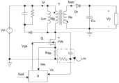
如图20所示的一种控制非隔离型BUCK类变流器输出电流的控制电路,包括:集成电路A、基准电压源U、变流器的输出电感Lo、可控开关Q和输出电感Lo的耦合绕组Na;As shown in Figure 20, a control circuit for controlling the output current of a non-isolated BUCK type converter includes: an integrated circuit A, a reference voltage source U, an output inductance Lo of the converter, a controllable switch Q and an output inductance Lo The coupling winding Na;
耦合绕组Na采集BUCK类变流器中激磁电感Lo上的电压信号,输出电压指示信号Va;The coupling winding Na collects the voltage signal on the excitation inductance Lo in the BUCK type converter, and outputs the voltage indication signal Va;
集成电路A的第一输入端与可控开关Q的输出端相连,并接收可控开关Q的电流信号Isw;The first input end of the integrated circuit A is connected to the output end of the controllable switch Q, and receives the current signal Isw of the controllable switch Q;
集成电路A的第二输入端接入输出激磁电感Lo的耦合绕组的一端电压,接收所述的电压指示信号Va;The second input end of the integrated circuit A is connected to the voltage at one end of the coupling winding of the output excitation inductance Lo, and receives the voltage indication signal Va;
集成电路A的第三输入端接收基准电压源U提供的基准电压信号Vref;基准电压信号Vref也可以选择在在集成电路A的内部实现;The third input terminal of the integrated circuit A receives the reference voltage signal Vref provided by the reference voltage source U; the reference voltage signal Vref can also be implemented inside the integrated circuit A;
集成电路A的输出端与可控开关Q的控制端相连,输出可控开关当前时刻的控制信号Vgs。The output terminal of the integrated circuit A is connected to the control terminal of the controllable switch Q, and outputs the control signal Vgs of the controllable switch at the current moment.
如图21所示,集成电路A包括:As shown in Figure 21, integrated circuit A includes:
RC滤波器A1、二极管导通时间检测电路A2、可控开关导通时间检测电路A3、乘法器A4、误差补偿电路A5和脉宽调制电路A6:RC filter A1, diode conduction time detection circuit A2, controllable switch conduction time detection circuit A3, multiplier A4, error compensation circuit A5 and pulse width modulation circuit A6:
RC滤波器A1的输入端11为集成电路A的第一输入端,接收可控开关的电流信号Isw;RC滤波器A2的输出端1与乘法器A4的第一输入端41相连并输出平均电流信号Iavg;The
二极管导通时间检测电路A2输入端21为集成电路A的第二输入端,接收电压指示信号Va;二极管导通时间检测电路A2的输出端2与乘法器A4的第二输入端42相连并输出二极管导通时间信号Ton_s;The
可控开关导通时间检测电路A3的输入端31接收可控开关上一时刻的控制信号Vgs,可控开关导通时间检测电路A3的输出端3与乘法器A4的第三输入端43相连并输出可控开关导通时间信号Ton_p;The
乘法器A4的第一输入端41接收平均电流信号Iavg,第二输入端42接收二极管导通时间信号Ton_s,第三输入端43接收输出端可控开关导通时间信号Ton_p,乘法器A4的输出端4与误差补偿电路A5的第一输入端51相连并输出输出电流信号Io;乘法器A4内部实现的计算公式为:Io=Iavg*(Ton_s+Ton_p)/Ton_p;The
误差补偿电路A5的第一输入端51接收输出电流信号Io,第二输入端52为集成电路A的第三输入端并接收一基准电压信号Vref;误差补偿电路A5的输出端5与脉宽调制电路A6的输入端61相连并输出误差信号Vea;The
脉宽调制电路A6的输出端61接收误差信号Vea,输出端6为集成电路A的输出端,输出可控开关当前时刻控制信号Vgs。The
如图22所示为本实施例电路的在CRM、DCM和CCM三种工作模式下的工作波形,其波形特征同实施例1。在本实施例中,所述的RC滤波器A1、二极管导通时间检测电路A2、可控开关导通时间检测电路A3、误差补偿电路A5和脉宽调制电路A6的具体电路结构与实施例1相同。As shown in FIG. 22 , the working waveforms of the circuit in this embodiment under the three working modes of CRM, DCM and CCM are the same as those in the first embodiment. In this embodiment, the specific circuit structure of the RC filter A1, the diode conduction time detection circuit A2, the controllable switch conduction time detection circuit A3, the error compensation circuit A5 and the pulse width modulation circuit A6 is the same as in
本实施例控制变流器输出电流的控制方法,包括以下步骤:The control method for controlling the output current of the converter in this embodiment includes the following steps:
(1)采集变流器中可控开关Q的电流信号Isw、变流器中与输出电感Lo相耦合的耦合绕组Na的电压信号、可控开关上一时刻的控制信号Vgs,并获取基准电压信号Vref;(1) Collect the current signal Isw of the controllable switch Q in the converter, the voltage signal of the coupling winding Na coupled with the output inductor Lo in the converter, the control signal Vgs of the controllable switch at the previous moment, and obtain the reference voltage Signal Vref;
(2)滤除可控开关电流信号Isw中的开关频率分量,得到平均电流信号Iavg;(2) Filter out the switching frequency component in the controllable switching current signal Isw to obtain the average current signal Iavg;
(3)对电压信号进行转换,得到电压指示信号Va;对电压指示信号Va进行检测,得到二极管导通时间信号Ton_s;(3) Convert the voltage signal to obtain the voltage indication signal Va; detect the voltage indication signal Va to obtain the diode conduction time signal Ton_s;
对电压指示信号Va进行检测包括如下步骤:Detecting the voltage indication signal Va includes the following steps:
(a)对电压指示信号Va进行过零检测,得到零电流检测信号ZCD;(a) Perform zero-crossing detection on the voltage indication signal Va to obtain a zero-current detection signal ZCD;
(b)对零电流检测信号ZCD进行脉宽检测,得到二极管导通时间信号Ton_s;(b) Perform pulse width detection on the zero current detection signal ZCD to obtain the diode conduction time signal Ton_s;
(4)对可控开关上一时刻的控制信号Vgs进行脉宽检测,得到可控开关导通时间信号Ton_p;(4) Perform pulse width detection on the control signal Vgs of the controllable switch at the previous moment, and obtain the conduction time signal Ton_p of the controllable switch;
(5)基于平均电流信号Iavg、二极管导通时间信号Ton_s和可控开关导通时间信号Ton_p,计算得到输出电流信号Io,(5) Based on the average current signal Iavg, the diode conduction time signal Ton_s and the controllable switch conduction time signal Ton_p, the output current signal Io is calculated,
其中,计算公式为:Among them, the calculation formula is:
Io=Iavg*(Ton_s+Ton_p)/Ton_p;Io=Iavg*(Ton_s+Ton_p)/Ton_p;
将输出电流信号Io与基准电压信号Vref进行比较,得到误差信号Vea;Comparing the output current signal Io with the reference voltage signal Vref to obtain the error signal Vea;
(6)将误差信号Vea进行调制得到可控开关Q当前时刻的控制信号Vgs,以控制变流器中可控开关Q的导通或关断,从而控制产生变流器输出电流值。(6) Modulate the error signal Vea to obtain the control signal Vgs of the controllable switch Q at the current moment, so as to control the turn-on or turn-off of the controllable switch Q in the converter, thereby controlling the output current value of the converter.
实施例6:Embodiment 6:
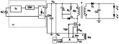
如图23所示是本发明应用于一种基于Triac调节输出电流的隔离型反激式电源的一个具体实施例;Triac调光电路用于实现输出电流的可调。As shown in FIG. 23 , it is a specific embodiment of the present invention applied to an isolated flyback power supply based on Triac to adjust the output current; the Triac dimming circuit is used to realize the adjustable output current.
Triac调光电路U1包括:依次串联的相控调光器Tr、EMI滤波器Em和整流桥z;Triac调光电路U1用于接收变流器交流输入信号,并输出一具有切相角的交流信号;基准电压调制电路U2,用于藕接至所述具有切相角的交流信号,基于所述切相角信号,输出所述的基准电压信号Vref;The Triac dimming circuit U1 includes: a phase-controlled dimmer Tr, an EMI filter Em, and a rectifier bridge z in series; the Triac dimming circuit U1 is used to receive the AC input signal of the converter and output an AC signal with a phase cut angle. signal; a reference voltage modulation circuit U2, configured to couple to the AC signal with a phase cut angle, and output the reference voltage signal Vref based on the phase cut angle signal;
在本实施例中,以交流输入电源(如通常的市电)经过Triac调光电路U1,利用整流桥,输出一直流电压,施加到所述反激式变流器。图23所示实施例中,EMI滤波器等是为防止电源对电网的干扰而施加,对本发明的具体实施没有影响。In this embodiment, the AC input power (such as common commercial power) passes through the Triac dimming circuit U1 and uses a rectifier bridge to output a DC voltage, which is applied to the flyback converter. In the embodiment shown in Fig. 23, the EMI filter and the like are applied to prevent the power supply from interfering with the power grid, and have no influence on the specific implementation of the present invention.
Triac调光电路通过对交流信号的导通角进行控制,控制施加到电源的输入电压,如图25所示。切相角越大,希望输出电流越小。由于输入电压为直流脉动电压,通常,反激变流器的输入电流也跟踪输入电压的波形信号(实现所谓的PFC控制),在一个工频(line frequency)周期内实现输出电流的平均值与基准电压相等。因此,为了调节输出电流的大小,可以通过改变基准电压信号Vref来实现。图24所示,其输出电流基准Vref与导通角成正比,最大值是全导通时的设定值Vref0,这对本领域技术人员而言是显而易见的。The Triac dimming circuit controls the conduction angle of the AC signal to control the input voltage applied to the power supply, as shown in Figure 25. The larger the phase-cut angle, the smaller the expected output current. Since the input voltage is a DC pulsating voltage, usually, the input current of the flyback converter also tracks the waveform signal of the input voltage (to realize the so-called PFC control), and the average value of the output current and the reference value are realized within one line frequency cycle. The voltages are equal. Therefore, in order to adjust the magnitude of the output current, it can be realized by changing the reference voltage signal Vref. As shown in FIG. 24 , the output current reference Vref is proportional to the conduction angle, and the maximum value is the set value Vref0 at full conduction, which is obvious to those skilled in the art.
其余实现方式,与实施例1等相同,这里不再详细描述。其PWM调制方式,为实现PFC功能,因此,其PWM调制可基于图26所示CRM PFC控制方式(带输入电压前馈)或者恒导通时间控制等方法。The rest of the implementation manners are the same as those in
以上虽然结合附图描述了本发明的实施方式,但是本领域普通技术人员可以在所附权利要求的范围内作出各种变更或修改。Although the embodiments of the present invention have been described above with reference to the accompanying drawings, those skilled in the art can make various changes or modifications within the scope of the appended claims.
Claims (9)
Priority Applications (1)
| Application Number | Priority Date | Filing Date | Title |
|---|---|---|---|
| CN 201110295481CN102355136B (en) | 2011-09-30 | 2011-09-30 | Control method and control circuit for controlling output current of converter |
Applications Claiming Priority (1)
| Application Number | Priority Date | Filing Date | Title |
|---|---|---|---|
| CN 201110295481CN102355136B (en) | 2011-09-30 | 2011-09-30 | Control method and control circuit for controlling output current of converter |
Publications (2)
| Publication Number | Publication Date |
|---|---|
| CN102355136Atrue CN102355136A (en) | 2012-02-15 |
| CN102355136B CN102355136B (en) | 2013-10-02 |
Family
ID=45578656
Family Applications (1)
| Application Number | Title | Priority Date | Filing Date |
|---|---|---|---|
| CN 201110295481ActiveCN102355136B (en) | 2011-09-30 | 2011-09-30 | Control method and control circuit for controlling output current of converter |
Country Status (1)
| Country | Link |
|---|---|
| CN (1) | CN102355136B (en) |
Cited By (9)
| Publication number | Priority date | Publication date | Assignee | Title |
|---|---|---|---|---|
| CN103730921A (en)* | 2013-11-18 | 2014-04-16 | 青岛盛嘉信息科技有限公司 | Charger |
| CN105763030A (en)* | 2014-12-17 | 2016-07-13 | 万国半导体(开曼)股份有限公司 | Circuit and method for inhibit excessive current during the starting phase of voltage converter |
| CN105846677A (en)* | 2015-02-03 | 2016-08-10 | 雅达电子国际有限公司 | DC-DC Power Converters Used in Datacom Distributed Power Architectures |
| CN106887959A (en)* | 2015-12-16 | 2017-06-23 | 立锜科技股份有限公司 | Power converter and switch control module therein |
| CN108736706A (en)* | 2018-08-01 | 2018-11-02 | 杭州老板电器股份有限公司 | Controllable switch power supply and purification water tank comprising the power supply |
| CN108988641A (en)* | 2017-06-01 | 2018-12-11 | 现代自动车株式会社 | Control the method for the onboard charger of vehicle and the onboard charger system of vehicle |
| CN109039093A (en)* | 2018-09-29 | 2018-12-18 | 杰华特微电子(杭州)有限公司 | Isolation type switching power supply and its control method |
| CN110190735A (en)* | 2019-06-21 | 2019-08-30 | 杰华特微电子(杭州)有限公司 | switching power supply |
| WO2025161752A1 (en)* | 2024-01-30 | 2025-08-07 | 深圳英集芯科技股份有限公司 | Control circuit |
Families Citing this family (1)
| Publication number | Priority date | Publication date | Assignee | Title |
|---|---|---|---|---|
| TWI499181B (en)* | 2013-10-25 | 2015-09-01 | Asian Power Devices Inc | Can be applied to the power factor correction converter control circuit module |
Citations (5)
| Publication number | Priority date | Publication date | Assignee | Title |
|---|---|---|---|---|
| US7352595B2 (en)* | 2005-11-08 | 2008-04-01 | System General Corp. | Primary-side controlled switching regulator |
| CN101777770A (en)* | 2010-02-12 | 2010-07-14 | 浙江大学 | Control circuit for voltage dropping type power factor corrector |
| CN101925237A (en)* | 2010-08-20 | 2010-12-22 | 杭州电子科技大学 | Primary Side Constant Current Control Device of Isolated Flyback Converter |
| CN201805600U (en)* | 2010-09-30 | 2011-04-20 | 杭州电子科技大学 | A LED driver primary side constant current control device |
| CN102186292A (en)* | 2011-04-30 | 2011-09-14 | 杭州电子科技大学 | Primary edge current reference generating circuit and method for high power factor constant-current switch power supply |
- 2011
- 2011-09-30CNCN 201110295481patent/CN102355136B/enactiveActive
Patent Citations (5)
| Publication number | Priority date | Publication date | Assignee | Title |
|---|---|---|---|---|
| US7352595B2 (en)* | 2005-11-08 | 2008-04-01 | System General Corp. | Primary-side controlled switching regulator |
| CN101777770A (en)* | 2010-02-12 | 2010-07-14 | 浙江大学 | Control circuit for voltage dropping type power factor corrector |
| CN101925237A (en)* | 2010-08-20 | 2010-12-22 | 杭州电子科技大学 | Primary Side Constant Current Control Device of Isolated Flyback Converter |
| CN201805600U (en)* | 2010-09-30 | 2011-04-20 | 杭州电子科技大学 | A LED driver primary side constant current control device |
| CN102186292A (en)* | 2011-04-30 | 2011-09-14 | 杭州电子科技大学 | Primary edge current reference generating circuit and method for high power factor constant-current switch power supply |
Cited By (14)
| Publication number | Priority date | Publication date | Assignee | Title |
|---|---|---|---|---|
| CN103730921A (en)* | 2013-11-18 | 2014-04-16 | 青岛盛嘉信息科技有限公司 | Charger |
| CN105763030A (en)* | 2014-12-17 | 2016-07-13 | 万国半导体(开曼)股份有限公司 | Circuit and method for inhibit excessive current during the starting phase of voltage converter |
| CN105763030B (en)* | 2014-12-17 | 2018-07-13 | 万国半导体(开曼)股份有限公司 | In the circuit and method that electric pressure converter startup stage inhibits electric current excessive |
| CN105846677A (en)* | 2015-02-03 | 2016-08-10 | 雅达电子国际有限公司 | DC-DC Power Converters Used in Datacom Distributed Power Architectures |
| US10862398B2 (en) | 2015-02-03 | 2020-12-08 | Astec International Limited | DC-DC power converter for use in data communications distributed power architecture |
| CN106887959B (en)* | 2015-12-16 | 2019-08-30 | 立锜科技股份有限公司 | Power converter and switch control module therein |
| CN106887959A (en)* | 2015-12-16 | 2017-06-23 | 立锜科技股份有限公司 | Power converter and switch control module therein |
| CN108988641A (en)* | 2017-06-01 | 2018-12-11 | 现代自动车株式会社 | Control the method for the onboard charger of vehicle and the onboard charger system of vehicle |
| CN108988641B (en)* | 2017-06-01 | 2023-04-07 | 现代自动车株式会社 | Method of controlling on-board charger of vehicle and on-board charger system of vehicle |
| CN108736706A (en)* | 2018-08-01 | 2018-11-02 | 杭州老板电器股份有限公司 | Controllable switch power supply and purification water tank comprising the power supply |
| CN109039093A (en)* | 2018-09-29 | 2018-12-18 | 杰华特微电子(杭州)有限公司 | Isolation type switching power supply and its control method |
| CN109039093B (en)* | 2018-09-29 | 2024-01-23 | 杰华特微电子股份有限公司 | Isolation type switching power supply and control method thereof |
| CN110190735A (en)* | 2019-06-21 | 2019-08-30 | 杰华特微电子(杭州)有限公司 | switching power supply |
| WO2025161752A1 (en)* | 2024-01-30 | 2025-08-07 | 深圳英集芯科技股份有限公司 | Control circuit |
Also Published As
| Publication number | Publication date |
|---|---|
| CN102355136B (en) | 2013-10-02 |
Similar Documents
| Publication | Publication Date | Title |
|---|---|---|
| CN102355136B (en) | Control method and control circuit for controlling output current of converter | |
| TWI508613B (en) | High efficiency LED driver circuit and its driving method | |
| CN102497711B (en) | LED drive circuit and comprise the Switching Power Supply of this drive circuit | |
| CN205160392U (en) | System for an equipment and be used for power conversion for power transistor driver of control power circuit | |
| US8670255B2 (en) | Utilization of a multifunctional pin combining voltage sensing and zero current detection to control a switched-mode power converter | |
| CN102364991B (en) | Switching power supply controller for constant current driving of LED by primary side control and method for constant current driving of LED | |
| US9502981B2 (en) | Enhanced power factor correction | |
| CN204131392U (en) | Boost power factor correction conversion circuit and control circuit thereof | |
| CN102946196B (en) | High power factor constant current driving circuit and constant-current device | |
| CN105991050A (en) | Method and device for high-power-factor flyback converter | |
| CN103716934A (en) | Driving circuit for driving light source, method and controller | |
| TW201308842A (en) | Buck converter and its control circuit and control method | |
| CN104967323B (en) | Low Output Voltage Ripple Discontinuous Mode Flyback Power Factor Correction Converter | |
| CN103716965A (en) | LED driving device and control circuit and output current detection circuit thereof | |
| CN104902648A (en) | LED light-adjustment circuit with silicon controlled rectifier, and light-adjustment method | |
| EP4106167B1 (en) | Control circuit and ac-dc power supply applying the same | |
| CN103683919A (en) | High-power-factor low-harmonic-distortion constant current circuit and device | |
| CN106655777A (en) | Switching power supply output cable pressure drop compensating circuit and compensating method | |
| CN202997938U (en) | A high power factor constant current drive circuit and a high power factor constant current device | |
| CN104702095A (en) | Switching power supply controller and switching power supply comprising switching power supply controller | |
| EP3459168A1 (en) | A bifred converter and a method of driving an output load | |
| TWI533745B (en) | Light source driving circuit, controller and method for controlling power converter | |
| CN106162998B (en) | A kind of LED drive controls circuit, control device and control method | |
| CN103716952B (en) | A kind of LED switch power supply and control method thereof | |
| Chen et al. | Evaluation of primary side control schemes for flyback converter with constant current output |
Legal Events
| Date | Code | Title | Description |
|---|---|---|---|
| C06 | Publication | ||
| PB01 | Publication | ||
| C10 | Entry into substantive examination | ||
| SE01 | Entry into force of request for substantive examination | ||
| C14 | Grant of patent or utility model | ||
| GR01 | Patent grant |