Movatterモバイル変換


[0]ホーム

URL:


CN102354519A - 3D semiconductor device - Google Patents

3D semiconductor device
Download PDF

Info

Publication number
CN102354519A
CN102354519ACN2011102198761ACN201110219876ACN102354519ACN 102354519 ACN102354519 ACN 102354519ACN 2011102198761 ACN2011102198761 ACN 2011102198761ACN 201110219876 ACN201110219876 ACN 201110219876ACN 102354519 ACN102354519 ACN 102354519A
Authority
CN
China
Prior art keywords
chip
data
hole
substrate
pad
Prior art date
Legal status (The legal status is an assumption and is not a legal conclusion. Google has not performed a legal analysis and makes no representation as to the accuracy of the status listed.)
Granted
Application number
CN2011102198761A
Other languages
Chinese (zh)
Other versions
CN102354519B (en
Inventor
姜郁成
张东铉
张星珍
李勋
金镇护
金南锡
文炳植
李于东
Current Assignee (The listed assignees may be inaccurate. Google has not performed a legal analysis and makes no representation or warranty as to the accuracy of the list.)
Samsung Electronics Co Ltd
Original Assignee
Samsung Electronics Co Ltd
Priority date (The priority date is an assumption and is not a legal conclusion. Google has not performed a legal analysis and makes no representation as to the accuracy of the date listed.)
Filing date
Publication date
Application filed by Samsung Electronics Co LtdfiledCriticalSamsung Electronics Co Ltd
Publication of CN102354519ApublicationCriticalpatent/CN102354519A/en
Application grantedgrantedCritical
Publication of CN102354519BpublicationCriticalpatent/CN102354519B/en
Activelegal-statusCriticalCurrent
Anticipated expirationlegal-statusCritical

Links

Images

Classifications

Landscapes

Abstract

A three-dimensional (3D) semiconductor device may include a stack of chips, including a master chip and one or more slave chips. I/O connections of slave chips need not be connected to channels on a motherboard, and only electrode pads of a master chip may be connected to the channels. Only the master chip may provide a load to the channels. A through-substrate via (TSV) boundary may be set on a data input path, a data output path, an address/command path, and/or a clock path of a semiconductor device in which the same type of semiconductor chips are stacked.

Description

Translated fromChinese
三维半导体器件3D semiconductor device

相关申请的交叉引用Cross References to Related Applications

本申请要求享受于2010年5月25日在韩国知识产权局提交、申请号为No.10-2010-0048616的韩国专利申请的优先权,其公开内容在此整体引入作为参考。This application claims the benefit of priority from Korean Patent Application No. 10-2010-0048616 filed with the Korean Intellectual Property Office on May 25, 2010, the disclosure of which is hereby incorporated by reference in its entirety.

技术领域technical field

本发明构思涉及半导体器件,更具体而言,涉及包括硅贯通孔(TSV)的三维(3D)半导体器件。The inventive concept relates to semiconductor devices, and more particularly, to three-dimensional (3D) semiconductor devices including through silicon vias (TSVs).

背景技术Background technique

随着如移动电话、数码相机、个人数字助理(PDA)等的数字信息设备产品变得越来越小和越来越轻并具有先进的功能和更高的性能,用在这些设备中的半导体封装也需要变小、变轻以及具有高集成度。用于在一个封装中提供多个半导体芯片的3D半导体技术已经引起重视。As digital information equipment products such as mobile phones, digital cameras, and personal digital assistants (PDAs) become smaller and lighter with advanced functions and higher performance, semiconductors used in these equipment Packages also need to be smaller, lighter, and highly integrated. 3D semiconductor technology for providing a plurality of semiconductor chips in one package has drawn attention.

发明内容Contents of the invention

这里公开一种包括基板贯通孔(TSV)的布置界面并具有去负载耦合(load-decoupled)结构的半导体器件。Disclosed herein is a semiconductor device including a layout interface of through-substrate vias (TSVs) and having a load-decoupled structure.

本发明还公开一种半导体器件,其中同样类型的半导体芯片层叠在一起并且它们可不同地配置。The present invention also discloses a semiconductor device in which semiconductor chips of the same type are stacked together and they can be configured differently.

本发明还公开一种半导体器件,其中具有相同原始电路设计的半导体芯片层叠在一起。The present invention also discloses a semiconductor device in which semiconductor chips having the same original circuit design are stacked together.

本发明还公开一种半导体器件,其中在芯片识别熔丝切除后可对晶圆(wafer)进行测试。The present invention also discloses a semiconductor device, wherein the wafer (wafer) can be tested after the chip identification fuse is cut off.

附图说明Description of drawings

通过下面详细描述,结合附图,可以更清楚地理解示例性实施例,其中:Exemplary embodiments can be more clearly understood from the following detailed description taken in conjunction with the accompanying drawings, in which:

图1示出了根据实施例的三维(3D)半导体器件;FIG. 1 shows a three-dimensional (3D) semiconductor device according to an embodiment;

图2是根据实施例的半导体存储器件的方块图;2 is a block diagram of a semiconductor memory device according to an embodiment;

图3示出了在图1所示的3D半导体器件的数据输入路径上设置硅贯通孔(TSV)界面(boundary)的操作;FIG. 3 shows the operation of setting a through-silicon via (TSV) interface (boundary) on the data input path of the 3D semiconductor device shown in FIG. 1;

图4示出了在图1所示的3D半导体器件的数据输出路径上设置TSV界面的可选方案;FIG. 4 shows an optional solution for setting a TSV interface on the data output path of the 3D semiconductor device shown in FIG. 1;

图5示出了在图1所示的3D半导体器件的命令/地址路径上设置TSV界面的可选方案;FIG. 5 shows an optional scheme for setting a TSV interface on the command/address path of the 3D semiconductor device shown in FIG. 1;

图6示出了在图1所示的3D半导体器件的时钟路径上设置TSV界面的可选方案;FIG. 6 shows an optional scheme of setting a TSV interface on the clock path of the 3D semiconductor device shown in FIG. 1;

图7示出了根据实施例的先入先出(FiFo)读取控制器;Figure 7 illustrates a first-in-first-out (FiFo) read controller, according to an embodiment;

图8示出了可选实施例;Figure 8 shows an alternative embodiment;

图9是如图7所示的先入先出读取控制器的操作时序图;FIG. 9 is an operation sequence diagram of the first-in-first-out reading controller shown in FIG. 7;

图10示出了如图1所示的3D半导体器件的全局控制操作;Fig. 10 shows the global control operation of the 3D semiconductor device shown in Fig. 1;

图11示出了如图10所示的用于控制全局控制电路的全局芯片选择信号发生电路;FIG. 11 shows a global chip selection signal generation circuit for controlling the global control circuit as shown in FIG. 10;

图12示出了根据实施例的全局命令发生器;Figure 12 shows a global command generator according to an embodiment;

图13示出了根据实施例的主芯片中的局部读取控制路径和全局读取控制路径;FIG. 13 shows a local read control path and a global read control path in the master chip according to an embodiment;

图14示出了根据实施例的TSV输入/输出(I/O)模块,其设计成使得主芯片的路径与从芯片的路径可彼此不同。FIG. 14 illustrates a TSV input/output (I/O) module, which is designed such that a path of a master chip and a path of a slave chip may be different from each other, according to an embodiment.

图15A和15B分别示出了根据实施例的包括不同元件的逻辑电路,这些元件符合基于包括具有相同物理性能的电路的芯片中多层的设计目的;15A and 15B respectively illustrate logic circuits according to embodiments including different elements that meet the design objectives based on multiple layers in a chip including circuits with the same physical properties;

图16示出了根据实施例的一个结构中的电晶片(Die)分类(EDS)级测试路径和封装级测试路径,其中主芯片和第一从芯片层叠在一起;FIG. 16 shows a Die Classification (EDS) level test path and a package level test path in a structure according to an embodiment, wherein the master chip and the first slave chip are stacked together;

图17和18分别示出了包括不同I/O类型(即输入态/输出态/三态)的逻辑电路,它们符合基于包括具有相同物理性能的电路的芯片中多层的设计目的;Figures 17 and 18 respectively show logic circuits comprising different I/O types (i.e. input state/output state/tri-state), which meet the design purpose based on multiple layers in a chip comprising circuits with the same physical performance;

图19示出了根据实施例的TSV到凸块气接方法,其防止凸块到晶圆后侧短路;FIG. 19 illustrates a TSV-to-bump air bonding method that prevents bump-to-wafer backside shorting, according to an embodiment;

图20示出了根据实施例的TSV到凸块气接方法,其防止凸块到晶圆后侧短路;20 illustrates a TSV-to-bump air bonding method that prevents bump-to-wafer backside shorting, according to an embodiment;

图21示出了根据实施例的层叠半导体芯片中的电路方块图,其用于晶圆测试中并可在封装工艺完成后停用;以及21 shows a block diagram of circuitry in a stacked semiconductor chip that is used in wafer testing and that can be disabled after the packaging process is complete, according to an embodiment; and

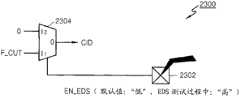
图22示出了根据实施例的逻辑电路,其中在芯片识别熔丝被切除后可使用探针测试点对晶圆进行测试。Figure 22 illustrates a logic circuit in which a probe test point can be used to test a wafer after chip identification fuses are cut, according to an embodiment.

具体实施方式Detailed ways

现在对示例性实施例进行详细的描述,这些示例性实施例如附图所示。然而,这些示例性实施例不限于下面示出的实施例,这里的实施例仅是被引入以提供对示例性实施例范围和精神的容易和完整理解。在这些附图中,为清楚起见,层和区域的厚度被放大。并且附图中的多种元件和区域被示意性地标出。因此,本发明构思不限于附图中绘出的相对尺寸或距离。附图中相似的附图标记表示相似的元件,并且因此不再重复对它们进行描述。Reference will now be made in detail to exemplary embodiments, which are illustrated in the accompanying drawings. However, these exemplary embodiments are not limited to the embodiments shown below, which are merely introduced to provide an easy and complete understanding of the scope and spirit of the exemplary embodiments. In the drawings, the thicknesses of layers and regions are exaggerated for clarity. Also, various elements and regions in the drawings are schematically labeled. Accordingly, the inventive concepts are not limited to the relative sizes or distances depicted in the drawings. Like reference numerals in the drawings denote like elements, and thus their descriptions will not be repeated.

应当理解的是,当元件或层被提及到“位于”、“连接到”、“耦合到”、“邻近”其它元件或层时,其可以直接地位于、连接到、耦合到或邻近其它元件或层,或者是可存在中间元件或层。相反地,当元件被提及到“直接地位于”、“直接地连接到”、“直接地耦合到”、“直接地邻近”其它元件或层或者类似描述时,则不存在中间元件或层。相似的附图标记从始至终都表示相似的元件。这里使用的术语“和/或”包括一个或多个相关列出术语的任意和所有组合。It should be understood that when an element or layer is referred to as being "located on," "connected to," "coupled to," or "adjacent" to another element or layer, it can be directly on, connected to, coupled to, or adjacent to the other element or layer. elements or layers, or intervening elements or layers may be present. In contrast, when an element is referred to as being "directly on," "directly connected to," "directly coupled to," "directly adjacent to" another element or layer, or the like, there are no intervening elements or layers present. . Like reference numerals designate like elements throughout. As used herein, the term "and/or" includes any and all combinations of one or more of the associated listed items.

应当理解的是,尽管术语第一、第二、第三等可用在这里描述多个元件、部件、区域、层和/或部分,但是这些元件、部件、区域、层和/或部分不应限于这些术语。这些术语仅用于区别一个元件、部件、区域、层或部分与另一个元件、部件、区域、层或部分。因此,下面讨论的第一元件、部件、区域、层或部分也可被称作为第二元件、部件、区域、层或部分,这并不脱离本发明构思的教义。It will be understood that although the terms first, second, third etc. may be used herein to describe various elements, components, regions, layers and/or sections, these elements, components, regions, layers and/or sections should not be limited to these terms. These terms are only used to distinguish one element, component, region, layer or section from another element, component, region, layer or section. Thus, a first element, component, region, layer or section discussed below could be termed a second element, component, region, layer or section without departing from the teachings of the present inventive concept.

如“之下”、“低于”、“下部”、“之上”、“上部”等的空间相对术语在此可被用于简便地描述图中所示的一个元件或结构与另一个元件或结构的关系。应当理解的是,这些空间相对术语还包括器件在使用或操作中处于如图所示的位置之外的不同位置。例如,如果图中的器件翻转,描述为“低于”或“之下”其它元件或结构的元件将会位于所述其它元件或结构之上。因此,术语“低于”可包括之上和之下两个方位。否则,器件可被定位(旋转90度或定位在其它位置)以及这里使用的空间相对描述可相应地解释。Spatially relative terms such as "under", "below", "lower", "above", "upper", etc. may be used herein for convenience in describing the relationship between one element or structure and another element shown in the figures. or structural relationships. It will be understood that these spatially relative terms also encompass different positions of the device in use or operation other than that illustrated. For example, if the device in the figures is turned over, elements described as "below" or "beneath" other elements or structures would then be oriented over the other elements or structures. Thus, the term "below" can encompass both an orientation of above and below. Otherwise, the device may be positioned (rotated 90 degrees or at other positions) and the spatially relative descriptions used herein interpreted accordingly.

这里使用的术语仅用于描述特定实施例的目的,并且并不意在限制本发明构思。这里所使用的单数形式“一个”以及“该”意在也包括复数形式,除非文中明确地指示不包括复数形式。应当进一步理解的是,对于术语“包括”和/或“包含”,当它们用在说明书中时,说明存在规定结构、整体、步骤、操作、元件、和/或部件,但是并不排除出现或者增加一个或多个其它结构、整体、步骤、操作、元件、部件、和/或其组。The terminology used herein is for the purpose of describing particular embodiments only and is not intended to limit the inventive concept. As used herein, the singular forms "a", "an" and "the" are intended to include the plural forms as well, unless the context clearly indicates otherwise. It should be further understood that, for the terms "comprising" and/or "comprising", when they are used in the specification, it means that there is a specified structure, integer, step, operation, element, and/or component, but it does not exclude the occurrence or Add one or more other structures, integers, steps, operations, elements, components, and/or groups thereof.

这里参考剖面性或透视性视图来描述实施例,这些视图是理想实施例(以及中间结构)的示意性视图。因此,可以预料到由于例如制造技术和/或公差的原因而在形状上与示意视图有一定的差异。因此,实施例应当被构造为不限于这里示出的区域的特定形状,而是还包括从例如制造原因而形成的形状偏差。例如,示出的具有尖锐边缘的边缘或角部区域可具有一定的圆形或弯曲形状。类似地,示出的为圆形或球形的元件可以是椭圆形或者可具有一定的直线或平坦部分。因此,附图中示出的区域本质上是示意性的,并且它们的形状并不意在限制公开实施例的范围。Embodiments are described herein with reference to cross-sectional or perspective illustrations that are schematic illustrations of idealized embodiments (and intermediate structures). Accordingly, certain deviations in shape from the schematic views as a result of, for example, manufacturing techniques and/or tolerances, are to be expected. Thus, embodiments should be constructed not to be limited to the particular shapes of regions illustrated herein but to include deviations in shapes that result, for example, from manufacturing. For example, edge or corner regions shown as having sharp edges may have a somewhat rounded or curved shape. Similarly, elements shown as circular or spherical may be oval or may have certain straight or flat portions. Thus, the regions shown in the figures are schematic in nature and their shapes are not intended to limit the scope of the disclosed embodiments.

除非相反地限定,这里使用的所有术语(包括技术术语和科学术语)具有与本发明构思所属领域技术人员的通常理解相同的含义。应当进一步理解的是,这些术语,如在通常使用词典中定义的那些,应当被解释为具有与其在相关技术文章中含义一致的含义,并且不应以理想化的或过度刻板的方式进行解释,除非这里有明显的限定。Unless defined to the contrary, all terms (including technical terms and scientific terms) used herein have the same meaning as commonly understood by those skilled in the art to which this inventive concept belongs. It should be further understood that these terms, as defined in commonly used dictionaries, should be interpreted as having meanings consistent with their meanings in relevant technical articles, and should not be interpreted in an idealized or overly rigid manner, Unless there is an obvious limit here.

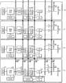
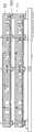
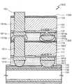
图1示出了根据一个实施例的三维(3D)半导体器件100。三维(3D)半导体器件100包括多个芯片110、120、130和140的层叠,它们配置在一个封装中,该多个芯片110、120、130和140通过基板贯通孔(TSV)连接部160进行通信。该多个芯片110、120、130和140层叠在基板150上。基板150可以为例如印刷电路板(PCB)(如聚酰亚胺、FR4等)或其它类型的基板。每个TSV连接部包括位于该多个芯片110、120、130和140中的每一个芯片中的基板贯通孔,其连接以形成单个节点,其中每个基板贯通孔包括穿过该芯片基板的至少一部分的贯通孔,该基板贯通孔也可(如图所示)穿透整个芯片。当基板贯通孔穿透该基板但并不穿透整个芯片时,该芯片还可包括将该基板贯通孔连接到芯片上表面的芯片焊盘或端子的导线。当该基板是硅基板时(如由结晶硅晶圆制成,其中在该晶圆上/内通过半导体工艺形成内部电路),该基板贯通孔可以是硅硅贯通孔。该基板贯通孔还可通过在半导体芯片制造中使用的其它基板形成,如绝缘器上硅、锗、锗化硅,砷化锗(GaAs)等。为简单起见在图1中仅示出了两个TSV连接部160。TSV连接部160可包括一个或多个数据用电极、一个地址用电极、命令用电极、电源用电极、接地用电极等。FIG. 1 illustrates a three-dimensional (3D)semiconductor device 100 according to one embodiment. A three-dimensional (3D)semiconductor device 100 includes a stack of a plurality ofchips 110 , 120 , 130 and 140 arranged in a package, the plurality ofchips 110 , 120 , 130 and 140 being connected by a through substrate via (TSV)connection 160 . communication. The plurality ofchips 110 , 120 , 130 and 140 are stacked on asubstrate 150 . Thesubstrate 150 may be, for example, a printed circuit board (PCB) (such as polyimide, FR4, etc.) or other types of substrates. Each TSV connection includes a through-substrate via in each of the plurality ofchips 110, 120, 130, and 140 connected to form a single node, wherein each through-substrate via includes at least A portion of the through-hole, the substrate through-hole may also (as shown) penetrate the entire chip. When the TSV penetrates the substrate but does not penetrate the entire chip, the chip may further include wires connecting the TSV to chip pads or terminals on the upper surface of the chip. When the substrate is a silicon substrate (eg, made of a crystalline silicon wafer on which internal circuits are formed by a semiconductor process), the substrate through-hole may be a silicon-silicon through-hole. The through-substrate vias can also be formed through other substrates used in semiconductor chip fabrication, such as silicon-on-insulator, germanium, silicon germanium, germanium arsenide (GaAs), and the like. For simplicity, only twoTSV connections 160 are shown in FIG. 1 . TheTSV connection part 160 may include one or more electrodes for data, an electrode for address, an electrode for command, an electrode for power, an electrode for ground, and the like.

第一到第四芯片110、120、130和140每个均包括第一表面112、122、132、142,它们分别是第一到第四芯片110、120、130和140的顶部表面,以及包括第二表面114、124、134和144,它们分别是第一到第四芯片110、120、130和140的底部表面。在图1中,由于这些芯片是以面朝下的方式层叠在一起的,芯片的顶部表面位于其芯片的相应底部表面之下。第一到第四芯片110、120、130和140的电路图案111(未示出)可设置在第一表面112、122、132和142上。第二表面114、124、134和144为第一到第四芯片110、120、130和140的晶圆后侧部。Each of the first tofourth chips 110, 120, 130, and 140 includes afirst surface 112, 122, 132, 142, which are top surfaces of the first tofourth chips 110, 120, 130, and 140, respectively, and includes The second surfaces 114, 124, 134 and 144, which are the bottom surfaces of the first tofourth chips 110, 120, 130 and 140, respectively. In FIG. 1, since the chips are stacked face-down, the top surfaces of the chips are below the corresponding bottom surfaces of the chips. Circuit patterns 111 (not shown) of the first tofourth chips 110 , 120 , 130 and 140 may be disposed on thefirst surfaces 112 , 122 , 132 and 142 . The second surfaces 114 , 124 , 134 and 144 are wafer backsides of the first tofourth chips 110 , 120 , 130 and 140 .

在这个例子中,第一芯片110直接地层叠在基板150上并用作主芯片。第二到第四芯片120、130和140层叠在主芯片110上并用作第一到第三从芯片。主芯片110和第一到第三从芯片120、130和140可以是相同类型或不同类型的芯片。例如,主芯片110和从芯片120、130和140可采用相同的掩模设计制成,采用相同制造工艺通过晶圆制备而沉积在钝化层上。因此,电路设计可以是相同的。可选地,可对主芯片110和从芯片120、130和140使用不同的电路设计。In this example, thefirst chip 110 is directly stacked on thesubstrate 150 and serves as a main chip. The second tofourth chips 120, 130 and 140 are stacked on themaster chip 110 and serve as first to third slave chips. Themaster chip 110 and the first tothird slave chips 120, 130 and 140 may be the same type or different types of chips. For example, themaster chip 110 and the slave chips 120, 130, and 140 may be fabricated using the same mask design, deposited on the passivation layer by wafer preparation using the same fabrication process. Therefore, the circuit design can be the same. Alternatively, different circuit designs may be used formaster chip 110 andslave chips 120 , 130 and 140 .

主芯片110和第一到第三从芯片120、130和140通过TSV连接部160彼此连接在一起。形成在主芯片110的第一表面112上的电极焊盘116a和116b通过凸块170a和170b而连接到主芯片110的电路图案111并连接到形成在基板150上的端子或电极152a和152b。形成在基板150上的电极152a和152b通过贯通孔154a和154b而连接到基板导线156a和156b以及焊接凸块158a和158b。焊接凸块158a和158b可连接到位于系统印刷电路板上的导线以形成通路,如存储模块电路板,从而将3D半导体器件100与外部设备(未示出)相连接。Themaster chip 110 and the first tothird slave chips 120 , 130 and 140 are connected to each other through theTSV connection part 160 .Electrode pads 116a and 116b formed onfirst surface 112 ofmain chip 110 are connected tocircuit pattern 111 ofmain chip 110 and to terminals orelectrodes 152a and 152b formed onsubstrate 150 throughbumps 170a and 170b. Theelectrodes 152a and 152b formed on thesubstrate 150 are connected to thesubstrate wires 156a and 156b and the solder bumps 158a and 158b through the throughholes 154a and 154b. The solder bumps 158a and 158b may be connected to wires on a system printed circuit board, such as a memory module circuit board, to form vias, thereby connecting the3D semiconductor device 100 with external devices (not shown).

第一到第三从芯片120、130和140的外部连接部不连接到该通路,而是仅连接到形成在主芯片110上的电极焊盘116a和116b。因此,只有主芯片110具有通路负载,并且与该3D半导体器件100通信的设备仅能观测到主芯片110的通路负载而不是所有四个芯片110、120、130和140的通路负载。与芯片以封装方式简单地层叠在一起的情况如双晶片封装(DDP)或四晶片封装(QDP)相比,第一到第三从芯片120、130和140对于通路是去负载耦合的,从而使得数据输入/输出速度可得到提高。External connection parts of the first tothird slave chips 120 , 130 and 140 are not connected to the via, but are connected only to theelectrode pads 116 a and 116 b formed on themaster chip 110 . Therefore, only themain chip 110 has a via load, and devices communicating with the3D semiconductor device 100 can only observe the via load of themain chip 110 and not all fourchips 110 , 120 , 130 and 140 . Compared with the case where chips are simply stacked together in a package, such as a dual die package (DDP) or a quad die package (QDP), the first tothird slave chips 120, 130, and 140 are deload-coupled to the vias, thereby The data input/output speed can be increased.

当主芯片110和第一到第三从芯片120、130和140为相同类型的芯片时,多个电路模块共用该主芯片110,如延迟同步电路模块、数据输入/输出电路模块、时钟电路模块等,此时第一到第三从芯片120、130和140的电路模块可不被使用并且因此处于关断状态。当主芯片110和第一到第三从芯片120、130和140为不同类型的芯片时,共用该主芯片110的电路模块可不在第一到第三从芯片120、130和140中设计和复制。与如DDP或QDP之类的芯片以传统封装方式简单地层叠在一起的情况相比,第一到第三从芯片120、130和140的功率消耗可以降低。并且,当主芯片110和第一到第三从芯片120、130和140是不同类型的芯片时,由于主芯片110的电路模块可不在第一到第三从芯片120、130和140中实现和复制,所以第一到第三从芯片120、130和140的尺寸可小于主芯片110的尺寸。When themaster chip 110 and the first tothird slave chips 120, 130 and 140 are the same type of chips, a plurality of circuit modules share themaster chip 110, such as delay synchronization circuit modules, data input/output circuit modules, clock circuit modules, etc. , at this time the circuit modules of the first tothird slave chips 120, 130 and 140 may not be used and thus be in an off state. When themaster chip 110 and the first tothird slave chips 120 , 130 and 140 are different types of chips, circuit modules sharing themaster chip 110 may not be designed and copied in the first tothird slave chips 120 , 130 and 140 . The power consumption of the first tothird slave chips 120, 130, and 140 may be reduced compared to a case where chips such as DDP or QDP are simply stacked together in a conventional package. Also, when themaster chip 110 and the first tothird slave chips 120, 130 and 140 are different types of chips, since the circuit modules of themaster chip 110 may not be implemented and copied in the first tothird slave chips 120, 130 and 140 , so the size of the first tothird slave chips 120 , 130 and 140 may be smaller than the size of themaster chip 110 .

下面参考附图2到6来详细地描述用于设置TSV位置的可选方案(下面称作为“用于设置TSV界面(boundary)的可选方案”),当主芯片110和第一到第三从芯片120、130和140为相同类型芯片时,通过该可选方案可实现第一到第三从芯片120、130和140的去负载耦合效应。将会在附图2中描述的半导体存储器件200可等效于主芯片110以及第一到第三从芯片120、130和140。An optional scheme for setting the TSV position (hereinafter referred to as "an optional scheme for setting the TSV interface (boundary)") is described in detail below with reference to accompanyingdrawings 2 to 6, when themain chip 110 and the first to the third slave When thechips 120 , 130 and 140 are of the same type, the de-load coupling effect of the first tothird slave chips 120 , 130 and 140 can be realized through this optional solution. Thesemiconductor memory device 200 which will be described in FIG. 2 may be equivalent to themaster chip 110 and the first tothird slave chips 120 , 130 and 140 .

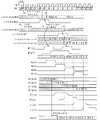
图2是示例性半导体存储器件200的方块图。参考图2,例如半导体存储器件200可以是动态随机存取存储(DRAM)芯片。半导体存储器件200包括其中配置有多个存储单元的存储单元阵列块DRAM核心205、寻址该多个存储单元的行译码器ROWDEC 237以及列译码器COLDEC 238、以及在存储单元阵列块DRAM核心205中写入数据并从其中读取数据的数据输入/输出驱动/感测放大器IODRV/IOSA 220。进一步,半导体存储器件200还包括数据输入/输出焊盘DQ、数据选通焊盘DQS、时钟焊盘CLK、命令焊盘CMD、以及地址焊盘ADDR。焊盘DQ、DQS、CLK、CMD、以及ADDR分别连接到缓冲器210、212、226、228、230、232和240。FIG. 2 is a block diagram of an exemplarysemiconductor memory device 200 . Referring to FIG. 2, for example, thesemiconductor memory device 200 may be a dynamic random access memory (DRAM) chip. Thesemiconductor memory device 200 includes a memory cell arrayblock DRAM core 205 in which a plurality of memory cells are configured, arow decoder ROWDEC 237 and acolumn decoder COLDEC 238 for addressing the plurality of memory cells, and a memory cell arrayblock DRAM core 205 for addressing the plurality of memory cells. A data input/output drive/sense amplifier IODRV/IOSA 220 in thecore 205 that writes and reads data from. Further, thesemiconductor memory device 200 also includes a data input/output pad DQ, a data strobe pad DQS, a clock pad CLK, a command pad CMD, and an address pad ADDR. Pads DQ, DQS, CLK, CMD, and ADDR are connected tobuffers 210, 212, 226, 228, 230, 232, and 240, respectively.

缓冲器230、232、240为输入缓冲器,其被连接以接收从芯片200的外部源输入的地址、命令和时钟信号。在这个例子中,缓冲器230、232和240直接地连接到地址芯片焊盘(ADDR)、命令芯片焊盘(CMD)和时钟芯片焊盘CLK。Thebuffers 230 , 232 , 240 are input buffers connected to receive address, command and clock signals input from external sources of thechip 200 . In this example, buffers 230, 232 and 240 are directly connected to address die pad (ADDR), command die pad (CMD) and clock die pad CLK.

缓冲器210和228构成数据输入/输出缓冲器,它们被连接以分别从芯片200的外部源接收数据以及输出数据到该外部源。在这个例子中,缓冲器210和228直接地连接到DQ芯片焊盘。缓冲器212被连接以接收来自芯片200的外部源的数据选通信号,以及缓冲器226被连接以输出数据选通信号到芯片200的外部源。Buffers 210 and 228 constitute data input/output buffers that are connected to receive data from and output data to, respectively, a source external tochip 200 . In this example, buffers 210 and 228 are directly connected to the DQ die pads.Buffer 212 is connected to receive a data strobe signal from a source external tochip 200 , and buffer 226 is connected to output a data strobe signal to a source external tochip 200 .

缓冲器210、212、226、228、230、232和240中的每个可包括多个缓冲电路部件中的一个或多个,以分别接收或发送其自身信号(每个缓冲电路部件可以是缓冲其自身单个信号的缓冲器)。例如,地址缓冲器230可包括18个缓冲电路部件,每个部件缓冲提供在各自地址芯片焊盘上的各自地址信号A0-A17。缓冲器210、212、226、228、230、232和240中的每个是否包括连接到多个芯片焊盘的多个缓冲器电路部件取决于芯片200的设计考虑,并且本发明不应被考虑为限于任何特定的缓冲器实施结构,除非有特别的说明。相似地,触发器FF 213、234和233可包括与缓冲器电路部件数量对应数量的多个触发器,其中各个触发器213、234或233分别连接到这些缓冲器电路部件。缓冲器210、212、226、228、230、232和240可被设计为通过差分信号与外部源通信,在这种情况下,每个缓冲器电路部件可连接到两个芯片焊盘并用于将单端信号变换为差分信号(如果配置为输出外部信号),或将差分信号变换为单端信号(如果配置为输入外部信号)。Each ofbuffers 210, 212, 226, 228, 230, 232, and 240 may include one or more of a plurality of buffer circuit components to receive or transmit its own signal, respectively (each buffer circuit component may be a buffer buffer for its own single signal). For example,address buffer 230 may include 18 buffer circuit components, each buffering a respective address signal A0-A17 provided on a respective address chip pad. Whether each ofbuffers 210, 212, 226, 228, 230, 232, and 240 includes multiple buffer circuit components connected to multiple chip pads depends on design considerations ofchip 200, and should not be considered in the present invention. Not limited to any particular buffer implementation unless otherwise stated. Similarly, the flip-flops FF 213, 234, and 233 may include a number of flip-flops corresponding to the number of buffer circuit parts to which the respective flip-flops 213, 234, or 233 are respectively connected.Buffers 210, 212, 226, 228, 230, 232, and 240 may be designed to communicate with external sources via differential signals, in which case each buffer circuit component may be connected to two die pads and used to connect Convert a single-ended signal to a differential signal (if configured to output an external signal), or convert a differential signal to a single-ended signal (if configured to input an external signal).

数据缓冲器210可包括n个缓冲器电路部件,其中每个连接到n个数据I/O焊盘DQ中的对应一个。顺序地输入到数据输入/输出焊盘DQ的多片n比特数据被传输到数据输入缓冲器210,以及被触发器FF 213锁存并顺序地输出到串并转换器DeSER 214。串并转换器DeSER 214顺序地接收m片n比特数据,并将该m片n比特数据输出为m×n比特并行数据。该串并转换器可通过n个串行到并行转换器来实现,这些转换器通过缓冲器210操作从n个数据I/O焊盘DQ中的对应一个接收到的m个顺序输入比特数据。m×n比特并行数据通过写入数据对准电路Wd ALIGN 216传输到数据输入/输出驱动/感测放大器IODRV/IOSA 220,该写入数据对准电路Wd ALIGN 216可调整m片n比特并行数据相对于存储单元阵列块DRAM核心205的行的位置。例如,Wd ALIGN 216可重新配置用于从DRAM核心205接收数据的局部I/O总线上的m片m比特并行数据。多片n比特数据可从DRAM核心205读取。例如,从存储单元阵列块DRAM核心205输出的并行读取数据可包括m片n比特数据。该m×n并行数据可被数据输入/输出驱动/感测放大器IODRV/IOSA 220放大。m片n比特数据的相对位置可通过读取数据对准电路222(下面称作为读取先入/先出(FIFO))进行调整。串行化器SER 224可将并行m×n比特数据转换为顺序的m片n比特数据。串行化器SER 224可包括n组并行到串行转换器,其中每个转换器操作m×n并行数据的m比特。顺序的m片n比特数据通过串行化器SER 224顺序地输出到数据输出缓冲器228,并且因此输出到n个数据I/O芯片焊盘DQ。作为一个例子,I/O数据焊盘DQ的数量可以是16(n=16)以及内部数据总线宽度可以为128(m=128)。作为另一个例子,数据I/O芯片焊盘的数量可以为4(n=4)以及内部数据总线宽度可以为16或32(m=4或8)。数据I/O芯片焊盘的数量可以大于16,如为32或者更多(n=32或n大于32)。可在本发明中实现的数据I/O焊盘结构的示例性细节可参见美国专利6930939以及7855926,它们整体引入于本发明作为参考。Thedata buffer 210 may include n buffer circuit parts, each of which is connected to a corresponding one of the n data I/O pads DQ. The pieces of n-bit data sequentially input to the data input/output pad DQ are transferred to thedata input buffer 210, and are latched by the flip-flop FF 213 and sequentially output to the serial-to-parallel converter DeSER 214. The serial-to-parallel converter DeSER 214 sequentially receives m pieces of n-bit data, and outputs the m pieces of n-bit data as m×n-bit parallel data. The serial-to-parallel converter may be implemented by n serial-to-parallel converters operating on m sequential input bit data received from a corresponding one of the n data I/O pads DQ through thebuffer 210 . The m×n-bit parallel data is transmitted to the data input/output drive/sensing amplifier IODRV/IOSA 220 through the write data alignmentcircuit Wd ALIGN 216, and the write data alignmentcircuit Wd ALIGN 216 can adjust m pieces of n-bit parallel data The position of the row of theDRAM core 205 relative to the memory cell array block. For example,Wd ALIGN 216 may reconfigure m slices of m-bit parallel data on the local I/O bus for receiving data fromDRAM core 205. Slices of n-bit data can be read from theDRAM core 205 . For example, the parallel read data output from the memory cell arrayblock DRAM core 205 may include m pieces of n-bit data. The m×n parallel data can be amplified by the data input/output drive/sense amplifier IODRV/IOSA 220. The relative position of m pieces of n-bit data can be adjusted by the read data alignment circuit 222 (hereinafter referred to as read first-in/first-out (FIFO)). Theserializer SER 224 can convert parallel m x n bit data into sequential m slices of n bit data.Serializer SER 224 may include n sets of parallel-to-serial converters, where each converter operates on m bits of mxn parallel data. Sequential m pieces of n-bit data are sequentially output to thedata output buffer 228 through theserializer SER 224, and thus output to the n data I/O die pads DQ. As an example, the number of I/O data pads DQ may be 16 (n=16) and the internal data bus width may be 128 (m=128). As another example, the number of data I/O chip pads may be 4 (n=4) and the internal data bus width may be 16 or 32 (m=4 or 8). The number of data I/O chip pads may be greater than 16, such as 32 or more (n=32 or n is greater than 32). Exemplary details of data I/O pad structures that may be implemented in the present invention can be found in US Pat. Nos. 6,930,939 and 7,855,926, which are incorporated herein by reference in their entirety.

输入到数据选通焊盘DQS的数据选通信号在通过数据输入缓冲器212后生成为输入数据选通信号,并用于控制触发器FF 213和串并转换器214。由半导体存储器件200的内部电路的操作所产生的输出数据选通信号通过输出缓冲器226输出到数据选通焊盘DQS。The data strobe signal input to the data strobe pad DQS is generated as an input data strobe signal after passing through thedata input buffer 212, and is used to control the flip-flop FF 213 and the serial-to-parallel converter 214. The output data strobe signal generated by the operation of the internal circuit of thesemiconductor memory device 200 is output to the data strobe pad DQS through theoutput buffer 226 .

输入到地址焊盘ADDR的地址信号通过数据输入缓冲器230和触发器FF 233而传输到地址缓冲器ADDRQ 235。输入到命令焊盘CMD的命令信号通过数据输入缓冲器232和触发器FF 234而传输到命令缓冲器和命令译码器CMDDEC CMDQ 236。传输到地址缓冲器ADDRQ 235的地址信号以及传输到命令缓冲器和命令译码器CMDDEC CMDQ 236的命令信号传输到行译码器ROWDEC 237和列译码器COLDEC 238,并用于激活字线和位线以选择存储单元。进一步,在命令缓冲器和命令译码器CMDDEC CMDQ 236中产生的命令控制信号被传输到缓冲器控制及时钟门控(gating)电路BUFFCONTROL&CLK GATING 250,并用于产生缓冲器控制信号和时钟门控信号。The address signal input to the address pad ADDR is transferred to theaddress buffer ADDRQ 235 through thedata input buffer 230 and the flip-flop FF 233. The command signal input to the command pad CMD is transmitted to the command buffer and commanddecoder CMDDEC CMDQ 236 through thedata input buffer 232 and the flip-flop FF 234. The address signal transmitted to theaddress buffer ADDRQ 235 and the command signal transmitted to the command buffer and commanddecoder CMDDEC CMDQ 236 are transmitted to therow decoder ROWDEC 237 and thecolumn decoder COLDEC 238, and are used to activate word lines and bits line to select a memory cell. Further, the command control signal generated in the command buffer and commanddecoder CMDDEC CMDQ 236 is transmitted to the buffer control and clock gating (gating)circuit BUFFCONTROL&CLK GATING 250, and is used to generate the buffer control signal and the clock gating signal .

输入到时钟焊盘CLK的时钟信号通过数据输入缓冲器240而被传输到时钟发生器及缓冲器电路CLK 242,并生成为多个内部时钟信号。在该时钟发生器和缓冲器电路CLK 242中产生的该多个内部时钟信号用于控制命令缓冲器及命令译码器CMDDEC CMDQ 236以及写入数据对准电路Wd ALIGN216。并且,内部时钟信号被提供给延迟同步电路DLL 260并用于控制串行化器SER 224和延迟控制器262。延迟控制器262控制读取FIFO Rd FIFO 222以响应在命令缓冲器和命令译码器CMDDEC CMDQ 236中产生的命令信号。在缓冲器控制及时钟门控电路BUFF CONTROL&CLK GATING 250中产生的缓冲器控制信号和时钟门控信号用于控制时钟发生器及缓冲器电路CLK242、延迟同步电路DLL 260、以及数据输入/输出缓冲器210、212、226、228、230、232和240。The clock signal input to the clock pad CLK is transmitted to the clock generator andbuffer circuit CLK 242 through thedata input buffer 240, and is generated as a plurality of internal clock signals. The multiple internal clock signals generated in the clock generator andbuffer circuit CLK 242 are used to control the command buffer and commanddecoder CMDDEC CMDQ 236 and the write data alignmentcircuit Wd ALIGN 216. Also, an internal clock signal is provided to the delaysynchronization circuit DLL 260 and used to control theserializer SER 224 and thedelay controller 262.Delay controller 262 controls readFIFO Rd FIFO 222 in response to command signals generated in command buffer and commanddecoder CMDDEC CMDQ 236. The buffer control signal and clock gating signal generated in the buffer control and clock gating circuit BUFF CONTROL &CLK GATING 250 are used to control the clock generator and buffer circuit CLK242, the delaysynchronization circuit DLL 260, and the data input/output buffer 210, 212, 226, 228, 230, 232 and 240.

尽管在上面的例子中数据芯片焊盘DQ、命令芯片焊盘CMD以及地址芯片焊盘ADDR被描述为分离的并彼此分开,但是这些数据、地址和/或命令信号可在共用芯片焊盘上被接收并被多路复用从而各自锁存(例如,如通过触发器电路233、234和213)。Although in the above examples the data die pad DQ, the command die pad CMD and the address die pad ADDR are described as separate and separated from each other, these data, address and/or command signals may be routed on the common die pad are received and multiplexed to be individually latched (eg, as by flip-flop circuits 233, 234, and 213).

3D半导体器件中的TSV界面可在一个或多个信号路径上形成,如数据输入路径、数据输出路径、命令/地址路径、时钟路径、延迟/DLL路径等。下面的描述是结合这样的3D半导体器件100来进行的,即其主芯片110和从芯片120、130和140与半导体存储器件200是相同的。然而,本发明和说明书可应用于这样的半导体芯片层叠,其中主和从芯片是相同的但是具有与半导体存储器件200的芯片不同的设计,或者其中主芯片与从芯片不同,和/或其中一部分或全部从芯片的设计彼此不同并且主芯片与所有或仅一些从芯片不同。A TSV interface in a 3D semiconductor device may be formed on one or more signal paths, such as a data input path, a data output path, a command/address path, a clock path, a delay/DLL path, and the like. The following description is made in conjunction with the3D semiconductor device 100 whosemaster chip 110 andslave chips 120 , 130 and 140 are the same as thesemiconductor memory device 200 . However, the present invention and description are applicable to semiconductor chip stacks in which the master and slave chips are the same but have a different design from the chips of thesemiconductor memory device 200, or in which the master chip is different from the slave chip, and/or a part thereof Or the designs of all slave chips are different from each other and the master chip is different from all or only some slave chips.

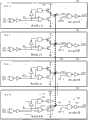
图3是示出了位于如图1所示的3D半导体器件100的数据路径上的基板贯通孔(TSV)连接部界面的多个可选方案的方块图。用于每个芯片110、120、130和140的数据输入路径包括数据输入/输出焊盘DQ、数据选通焊盘DQS、数据输入缓冲器210、数据选通输入缓冲器212、串并转换器DeSER 214、写入数据对准电路Wd ALIGN 216、数据输入/输出驱动/感测放大器IODRV/IOSA220、以及存储单元阵列块DRAM核心205。FIG. 3 is a block diagram illustrating several alternatives for a through-substrate via (TSV) connection interface on a data path of the3D semiconductor device 100 as shown in FIG. 1 . The data input path for eachchip 110, 120, 130, and 140 includes a data input/output pad DQ, a data strobe pad DQS, adata input buffer 210, a datastrobe input buffer 212, a serial-to-parallel converter DeSER 214, write data alignmentcircuit Wd ALIGN 216, data input/output drive/sense amplifier IODRV/IOSA 220, and memory cell arrayblock DRAM core 205.

在数据输入路径上,TSV连接部160的位置可在几个界面可选方案中设置。图3示出了TSV位置的5个可选方案(方案Ⅰ-Ⅴ)。应当注意的是,一个可选方案(方案Ⅰ-Ⅴ中的一个)就足以实现从主芯片到从芯片数据输入路径的TSV连接部。尽管图3中示出的多种可选方案并不是相互排除的,但是单个可选方案可在特定的3D半导体器件中实现以及并不需要实现其它剩余可选方案。然而,为了易于说明,所有的可选方案都在单个图中示出。On the data input path, the location of theTSV connection 160 can be set in several interface options. Figure 3 shows five alternatives for the location of TSVs (Schemes I-V). It should be noted that one alternative (one of schemes I-V) is sufficient to implement the TSV connection from the master chip to the slave chip data input path. Although the various options shown in FIG. 3 are not mutually exclusive, a single option may be implemented in a particular 3D semiconductor device and the other remaining options need not be implemented. However, for ease of illustration, all alternatives are shown in a single figure.

方案Ⅰ表示穿过每个数据输入/输出焊盘DQ的TSV连接部以及穿过数据选通焊盘DQS的TSV连接部。可选地,方案Ⅰ的TSV连接部可实现在数据输入/输出焊盘DQ与缓冲器210之间的信号路径(如连接到数据输入/输出焊盘DQ的导线)的任何地方,以及相似地,在芯片焊盘DQS和缓冲器212之间的信号路径之间的任何地方。因此,如果芯片110、120、130和140的设计提供16个DQ I/O焊盘DQ0-DQ 15以及一个DQS芯片焊盘,则方案Ⅰ表示穿过芯片110、120、130和140的DQ0的TSV连接部、穿过这些芯片的DQ1的TSV连接部、以及用于这些芯片的DQn输入/输出芯片焊盘群的每一个的各个TSV连接部。方案Ⅰ还可包括穿过芯片110、120、130和140中每一个的每个DQS芯片焊盘的TSV连接部。Scheme I represents a TSV connection through each data input/output pad DQ and a TSV connection through the data strobe pad DQS. Alternatively, the TSV connection of Scheme I may be implemented anywhere in the signal path between the data input/output pad DQ and the buffer 210 (such as a wire connected to the data input/output pad DQ), and similarly , anywhere between the signal path between die pad DQS andbuffer 212 . Thus, if the design ofchips 110, 120, 130, and 140 provides for 16 DQ I/O pads DQ0-DQ 15 and one DQS chip pad, Scenario I represents the TSV connections, TSV connections through DQ1 of these chips, and individual TSV connections for each of the DQn input/output chip pad groups of these chips. Scheme I may also include a TSV connection through each of the DQS die pads of each of thechips 110 , 120 , 130 , and 140 .

方案Ⅱ表示分别连接位于对应的数据输入缓冲器210与触发器FF 213(用于数据信号)之间的每个芯片的几个对应数据信号路径的TSV连接部160,以及连接到每个芯片的数据选通输入缓冲器212的输出的TSV连接部。方案Ⅲ表示分别连接位于对应的触发器FF 213的输出之间以及位于串并转换器DeSER 214和/或写入数据对准电路Wd ALIGN 216之前的每个芯片的几个对应数据信号路径的TSV连接部160。方案Ⅳ表示分别连接位于串并转换器DeSER 214和/或写入数据对准电路Wd ALIGN 216的输出与数据输入/输出驱动/感测放大器IODRV/IOSA 220之间的每个芯片的几个对应数据信号路径的TSV连接部160。可以理解的是,本发明可以应用于没有串并转换器DeSER214和写入数据对准电路Wd ALIGN 216的芯片设计场合。在这种情况下,方案Ⅲ和方案Ⅳ可表示相同的TSV连接部160。方案Ⅴ表示分别连接位于数据输入/输出驱动/感测放大器IODRV/IOSA 220与存储阵列(包括DRAM 205)之间的每个芯片的几个对应数据信号路径的TSV连接部160。Scheme II represents theTSV connections 160 respectively connecting several corresponding data signal paths of each chip between the correspondingdata input buffer 210 and the flip-flop FF 213 (for data signals), and theTSV connections 160 connected to each chip The data strobe is input to the TSV connection of the output ofbuffer 212 . Scheme III represents connecting the TSVs of several corresponding data signal paths of each chip between the outputs of the corresponding flip-flops FF 213 and before the serial-to-parallel converter DeSER 214 and/or write data alignmentcircuit Wd ALIGN 216 respectivelyConnecting part 160. Scheme IV represents several correspondences of each chip respectively connected between the output of the serial-to-parallel converter DeSER 214 and/or the write data alignmentcircuit Wd ALIGN 216 and the data input/output drive/sense amplifier IODRV/IOSA 220TSV connection portion 160 of the data signal path. It can be understood that the present invention can be applied to chip design occasions without serial-to-parallel converter DeSER214 and write data alignmentcircuit Wd ALIGN 216. In this case, Scheme III and Scheme IV may represent the sameTSV connection part 160 . Scheme V represents theTSV connections 160 respectively connecting several corresponding data signal paths of each chip between the data input/output drive/sense amplifier IODRV/IOSA 220 and the memory array (including the DRAM 205).

当主芯片110和第一到第三从芯片120、130和140层叠并且TSV连接部160如方案Ⅰ、方案Ⅱ、方案Ⅲ、方案Ⅳ和方案Ⅴ那样布置时,第一到第三从芯片120、130和140的一些电路可不使用。例如,当TSV 160的位置设置在数据输入/输出焊盘之后时(方案Ⅰ的可选实施),可不使用(或不需要使用)第一到第三从芯片120、130和140的数据输入/输出焊盘DQ和数据选通焊盘DQS。主芯片110的数据输入/输出焊盘DQ以及数据选通焊盘DQS可被第一到第三从芯片120、130和140共用,并且第一到第三从芯片120、130和140可通过主芯片110的数据输入/输出焊盘DQ以及对应的TSV连接部160来接收数据。主芯片110的数据输入/输出焊盘DQ以及数据选通焊盘DQS可连接到3D半导体器件100(参见图1)的电极焊盘116a和116b。When themaster chip 110 and the first tothird slave chips 120, 130 and 140 are stacked and theTSV connection portion 160 is arranged as in the scheme I, scheme II, scheme III, scheme IV and scheme V, the first to thethird slave chips 120, Some circuits of 130 and 140 may not be used. For example, when the position ofTSV 160 is set behind the data input/output pad (optional implementation of scheme I), the data input/output of first tothird slave chips 120, 130 and 140 may not be used (or need not be used). output pad DQ and data strobe pad DQS. The data input/output pad DQ and the data strobe pad DQS of themaster chip 110 may be shared by the first tothird slave chips 120, 130 and 140, and the first tothird slave chips 120, 130 and 140 may be passed through the master chip. The data input/output pads DQ of thechip 110 and thecorresponding TSV connection 160 receive data. The data input/output pad DQ and the data strobe pad DQS of themain chip 110 may be connected to theelectrode pads 116 a and 116 b of the 3D semiconductor device 100 (see FIG. 1 ).

当TSV连接部160的位置被设置为如第二界面方案Ⅱ时,第一到第三从芯片120、130和140的数据输入/输出焊盘DQ、数据选通焊盘DQS、数据输入缓冲器210以及数据选通输入缓冲器212都不需要使用。主芯片110的数据输入/输出焊盘DQ、数据选通焊盘DQS、数据输入缓冲器210以及数据选通输入缓冲器212可被第一到第三从芯片120、130和140共用。When the position of theTSV connection part 160 is set as the second interface scheme II, the data input/output pads DQ, data strobe pads DQS, and data input buffers of the first tothird slave chips 120, 130, and 140 210 and datastrobe input buffer 212 need not be used. The data input/output pad DQ, the data strobe pad DQS, thedata input buffer 210 and the datastrobe input buffer 212 of themaster chip 110 may be shared by the first tothird slave chips 120 , 130 and 140 .

当TSV连接部160的位置被设置为如第三界面方案Ⅲ时,第一到第三从芯片120、130和140的数据输入/输出焊盘DQ、数据选通焊盘DQS、数据输入缓冲器210、数据选通输入缓冲器212以及触发器FF 213都不需要使用。主芯片110的数据输入/输出焊盘DQ、数据选通焊盘DQS、数据输入缓冲器210、数据选通输入缓冲器212以及触发器FF 213可被第一到第三从芯片120、130和140共用。When the position of theTSV connection part 160 is set as the third interface scheme III, the data input/output pads DQ, data strobe pads DQS, and data input buffers of the first tothird slave chips 120, 130, and 140 210, datastrobe input buffer 212 and flip-flop FF 213 do not need to be used. The data input/output pad DQ ofmaster chip 110, data strobe pad DQS,data input buffer 210, datastrobe input buffer 212 and flip-flop FF 213 can be first to the 3rd from chip 120,130 and 140 shared.

当TSV连接部160的位置被设置为如第四界面方案Ⅳ时,第一到第三从芯片120、130和140的数据输入/输出焊盘DQ、数据选通焊盘DQS、数据输入缓冲器210、数据选通输入缓冲器212、触发器FF 213、串并转换器214、以及写入数据对准电路Wd ALIGN 216都不需要使用。主芯片110的数据输入/输出焊盘DQ、数据选通焊盘DQS、数据输入缓冲器210、数据选通输入缓冲器212、触发器FF 213、串并转换器214、以及写入数据对准电路WdALIGN 216可被第一到第三从芯片120、130和140共用。When the position of theTSV connection part 160 is set as the fourth interface scheme IV, the data input/output pads DQ, data strobe pads DQS, and data input buffers of the first tothird slave chips 120, 130, and 140 210, the datastrobe input buffer 212, the flip-flop FF 213, the serial-to-parallel converter 214, and the write data alignmentcircuit Wd ALIGN 216 do not need to be used. Data input/output pad DQ, data strobe pad DQS,data input buffer 210, datastrobe input buffer 212, flip-flop FF 213, serial-to-parallel converter 214, and write data alignment ofmain chip 110 Thecircuit WdALIGN 216 can be shared by the first tothird slave chips 120 , 130 and 140 .

当TSV连接部160的位置被设置为如第五界面方案Ⅴ时,第一到第三从芯片120、130和140的数据输入/输出焊盘DQ、数据选通焊盘DQS、数据输入缓冲器210、数据选通输入缓冲器212、触发器FF 213、串并转换器214、写入数据对准电路Wd ALIGN 216、以及数据输入/输出驱动/感测放大器IODRV/IOSA 220都不需要使用。主芯片110的数据输入/输出焊盘DQ、数据选通焊盘DQS、数据输入缓冲器210、数据选通输入缓冲器212、触发器FF213、串并转换器214、写入数据对准电路Wd ALIGN 216、以及数据输入/输出驱动/感测放大器IODRV/IOSA 220可被第一到第三从芯片120、130和140共用。对于方案Ⅰ、方案Ⅱ、方案Ⅲ、方案Ⅳ和方案Ⅴ中的每一种方案,自芯片焊盘到从芯片内部数据输入路径的一位置处的从芯片数据输入路径的一部分可不使用。例如,当该3D半导体器件被封装在半导体封装内时(如被包在保护模制材料中),数据芯片焊盘DQ可不具有任何外部导体连接部以及任何用于输入数据信号的信号连接部。When the position of theTSV connection part 160 is set as the fifth interface scheme V, the data input/output pads DQ, data strobe pads DQS, and data input buffers of the first tothird slave chips 120, 130, and 140 210, datastrobe input buffer 212, flip-flop FF 213, serial-to-parallel converter 214, write data alignmentcircuit Wd ALIGN 216, and data input/output drive/sense amplifier IODRV/IOSA 220 are not required to be used. Data input/output pad DQ, data strobe pad DQS,data input buffer 210, datastrobe input buffer 212, flip-flop FF213, serial-to-parallel converter 214, write data alignment circuit Wd ofmain chip 110 TheALIGN 216 and the data input/output drive/sense amplifier IODRV/IOSA 220 can be shared by the first tothird slave chips 120 , 130 and 140 . For each of Scheme I, Scheme II, Scheme III, Scheme IV and Scheme V, a part of the slave chip data input path at a position from the chip pad to the slave chip internal data input path may not be used. For example, when the 3D semiconductor device is packaged in a semiconductor package (such as encased in a protective molding material), the data die pad DQ may not have any external conductor connections and any signal connections for inputting data signals.

方案Ⅰ、方案Ⅱ、方案Ⅲ、方案Ⅳ和方案Ⅴ中,从数据输出路径的内部位置到芯片焊盘DQ的数据输出路径的一部分可不使用。例如,当该3D半导体器件被封装在半导体封装内时(如被包在保护模制材料中),数据芯片焊盘DQ可不具有任何外部导体连接部以及不能传输封装外部的数据信号。In Scheme I, Scheme II, Scheme III, Scheme IV and Scheme V, a part of the data output path from the inner position of the data output path to the chip pad DQ may not be used. For example, when the 3D semiconductor device is packaged in a semiconductor package (such as encased in a protective molding material), the data die pad DQ may not have any external conductor connections and cannot transmit data signals outside the package.

表1示出了当在具有四个数据I/O芯片焊盘DQ的芯片110、120、130和140的数据输入路径上实现方案Ⅰ、方案Ⅱ、方案Ⅲ、方案Ⅳ和方案Ⅴ的TSV连接部160时,采用器件200作为主芯片110以及作为从芯片120、130和140的3D半导体器件100的比较例子的特性。Table 1 shows the TSV connections of Scheme I, Scheme II, Scheme III, Scheme IV and Scheme V when implemented on the data input paths ofchips 110, 120, 130 and 140 with four data I/Ochip pads DQ 160 , the characteristics of a comparative example of thedevice 200 as themaster chip 110 and the3D semiconductor device 100 as the slave chips 120 , 130 and 140 are used.

[表1][Table 1]

如表1所示,由于TSV 160的位置从第一界面方案Ⅰ至第五界面方案Ⅴ逐渐接近,所以数据窗口对于从芯片变得更宽,数据设置/保持时间tDS/DH得到改善,并且可提供去负载耦合效应。然而,随着TSV连接部160的位置从第一界面方案Ⅰ逐渐接近至第五界面方案Ⅴ,TSV 160的数量会增加。As shown in Table 1, since the position ofTSV 160 is gradually approaching from the first interface scheme I to the fifth interface scheme V, the data window becomes wider for the slave chip, the data setup/hold time tDS/DH is improved, and can be Provides de-load coupling effects. However, as the position of theTSV connection portion 160 gradually approaches from the first interface scheme I to the fifth interface scheme V, the number ofTSVs 160 will increase.

图4示出了在如图1所示的3D半导体器件100的数据输出路径上的TSV位置的5个可选方案(方案Ⅰ-Ⅴ)。应当注意的是,一个可选方案(方案Ⅰ-Ⅴ中的一个)就足以实现从芯片到主芯片的数据输出路径的TSV连接部。尽管如图4所示的多个可选方案可能不是相互排除的,但是单个可选方案(即仅方案Ⅰ-Ⅴ中的一个)可在特定3D半导体器件上实现,并且其它剩余可选方案不需要实现。然而,为了便于说明,在单个图中示出了所有可选方案。FIG. 4 shows five optional schemes (Schemes I-V) for the position of TSVs on the data output path of the3D semiconductor device 100 shown in FIG. 1 . It should be noted that one alternative (one of schemes I-V) is sufficient to realize the TSV connection of the data output path from chip to master chip. Although the multiple options shown in Figure 4 may not be mutually exclusive, a single option (i.e. only one of options I-V) can be implemented on a particular 3D semiconductor device, and the other remaining options are not need to be realized. However, for ease of illustration, all alternatives are shown in a single figure.

参考图4,主芯片110和每个从芯片120、130和140的数据输出路径包括存储单元阵列块DRAM核205、数据输入/输出驱动/感测放大器IODRV/IOSA 220、读取FIFO 222、串行化器SER 224、数据选通输出缓冲器226、数据输出缓冲器228、数据选通焊盘DQS、以及数据输入/输出焊盘DQ。With reference to Fig. 4, the data output path ofmaster chip 110 and eachslave chip 120, 130 and 140 comprises memory cell arrayblock DRAM core 205, data input/output driver/sensing amplifier IODRV/IOSA 220, readsFIFO 222,serial Rowizer SER 224, datastrobe output buffer 226,data output buffer 228, data strobe pad DQS, and data input/output pad DQ.

在数据输出路径上,TSV连接部160的位置可根据几个界面可选方案中的一个来设定。例如,在第五界面可选方案(方案Ⅴ)中,TSV连接部160中的每一个可连接到位于DRAM 205与数据输入/输出驱动/感测放大器IODRV/IOSA 220之间的数据输出路径的相应节点。在第四界面可选方案(方案Ⅳ)中,TSV连接部160中的每一个可连接到位于数据输入/输出驱动/感测放大器IODRV/IOSA 220与数据输入/输出驱动/感测放大器IODRV/IOSA 220之间的数据输出路径的相应节点。例如,方案Ⅳ的这些节点可紧跟在数据输入/输出驱动/感测放大器IODRV/IOSA 220之后或紧跟在读取FIFO 222之前。在第三界面可选方案(方案Ⅲ)中,TSV连接部160中的每一个可连接到读取FIFO 222的相应的一个存储节点或连接到FIFO 220的相应的一个输出节点(如图4所示)。例如,如果FIFO 222包括多个触发器锁存器以存储将要输出的数据,则TSV连接部160可连接到这些触发器型锁存器中每一个的相应的几个Q或Q汇流条节点。在第二界面可选方案(方案Ⅱ)中,TSV连接部160可连接到位于串行化器SER 224与缓冲器228之间的数据输出路径的相应节点,如紧跟在串行化器224之后或正好位于缓冲器228之前的节点。在第一界面可选方案(方案Ⅰ)中,TSV连接部可连接到相应数据输入/输出焊盘DQ和数据选通焊盘DQS或连接到位于数据输入/输出焊盘DQ和/或数据选通焊盘DQS之前的数据输出路径的相应位置。On the data output path, the location of theTSV connection 160 can be set according to one of several interface options. For example, in a fifth interface option (Scheme V), each of theTSV connections 160 may be connected to a data output path between theDRAM 205 and the data input/output drive/sense amplifier IODRV/IOSA 220 corresponding node. In the fourth interface option (Scheme IV), each of theTSV connections 160 can be connected to the data input/output drive/sense amplifier IODRV/IOSA 220 and the data input/output drive/sense amplifier IODRV/ Corresponding nodes of data output paths betweenIOSAs 220. For example, these nodes of scheme IV may immediately follow the data input/output drive/sense amplifier IODRV/IOSA 220 or immediately precede theread FIFO 222. In the third interface optional scheme (scheme III), each of theTSV connection parts 160 can be connected to a corresponding storage node of theread FIFO 222 or to a corresponding output node of the FIFO 220 (as shown in FIG. 4 Show). For example, ifFIFO 222 includes multiple flip-flop latches to store data to be output,TSV connection 160 may be connected to a corresponding few Q or Q bus bar nodes of each of these flip-flop latches. In a second interface option (Scheme II), theTSV connection 160 can be connected to a corresponding node in the data output path between theserializer SER 224 and thebuffer 228, such as immediately after theserializer 224 Nodes after or just beforebuffer 228 . In the first interface optional scheme (Scheme Ⅰ), the TSV connection part can be connected to the corresponding data input/output pad DQ and data strobe pad DQS or connected to the data input/output pad DQ and/or data selection pad DQS. The corresponding position of the data output path before the pad DQS.

当主芯片110和第一到第三从芯片120、130和140相层叠,并且TSV连接部160的位置被分别设置为如第一到第五界面方案Ⅰ、方案Ⅱ、方案Ⅲ、方案Ⅳ和方案Ⅴ时,第一到第三从芯片120、130和140中的TSV界面的外部电路块可不使用。换句话说,当TSV连接器160的位置被设置为如第一界面方案Ⅰ而位于数据输入/输出焊盘DQ或数据选通焊盘DQS之前的相应位置时,第一到第三从芯片120、130和140的数据输入/输出焊盘DQ或数据选通焊盘DQS可不使用。主芯片110的数据输入/输出焊盘DQ和数据选通焊盘DQS可与第一到第三从芯片120、130和140共用。主芯片110的数据输入/输出焊盘DQ和数据选通焊盘DQS可连接到该3D半导体器件100的电极焊盘116a和116b。When themaster chip 110 and the first tothird slave chips 120, 130 and 140 are stacked, and the positions of theTSV connection parts 160 are respectively set as the first to fifth interface scheme I, scheme II, scheme III, scheme IV and scheme When V, the external circuit blocks of the TSV interface in the first tothird slave chips 120, 130 and 140 may not be used. In other words, when the position of theTSV connector 160 is set to a corresponding position before the data input/output pad DQ or the data strobe pad DQS as in the first interface scheme I, the first tothird slave chips 120 , 130 and 140 data input/output pad DQ or data strobe pad DQS may not be used. The data input/output pad DQ and the data strobe pad DQS of themaster chip 110 may be shared with the first tothird slave chips 120 , 130 and 140 . Data input/output pads DQ and data strobe pads DQS of themain chip 110 may be connected toelectrode pads 116 a and 116 b of the3D semiconductor device 100 .

当TSV连接部160的位置按照第二界面方案Ⅱ设置时,第一到第三从芯片120、130和140的数据选通输出缓冲器226、数据输出缓冲器228、数据选通焊盘DQS、以及数据输入/输出焊盘DQ不需要使用。主芯片110的数据选通输出缓冲器226、数据输出缓冲器228、数据输入/输出焊盘DQ以及数据选通焊盘DQS与第一到第三从芯片120、130和140共用。When the position of theTSV connection part 160 is set according to the second interface scheme II, the datastrobe output buffer 226, thedata output buffer 228, the data strobe pad DQS, And the data input/output pad DQ need not be used. The datastrobe output buffer 226 , thedata output buffer 228 , the data input/output pad DQ, and the data strobe pad DQS of themaster chip 110 are shared with the first tothird slave chips 120 , 130 and 140 .

当TSV连接部160的位置按照第三界面方案Ⅲ设置时,放置在读取FIFO222的存储节点之后的电路块,即第一到第三从芯片120、130和140的串行化器SER 224、数据选通输出缓冲器226、数据输出缓冲器228、数据选通焊盘DQS、以及数据输入/输出焊盘DQ不需要使用。放置在读取FIFO 222的存储节点之后的电路块,即主芯片110的串行化器SER 224、数据选通输出缓冲器226、数据输出缓冲器228、数据选通焊盘DQS以及数据输入/输出焊盘DQ与第一到第三从芯片120、130和140共用。When the position of theTSV connection part 160 is set according to the third interface scheme III, the circuit block placed after the storage node of theread FIFO 222, that is, theserializer SER 224, the first to thethird slave chips 120, 130 and 140 The datastrobe output buffer 226, thedata output buffer 228, the data strobe pad DQS, and the data input/output pad DQ need not be used. The circuit block placed after the storage node of theread FIFO 222, that is, theserializer SER 224 of themain chip 110, the datastrobe output buffer 226, thedata output buffer 228, the data strobe pad DQS and the data input/output buffer The output pad DQ is shared with the first tothird slave chips 120 , 130 and 140 .

当TSV连接部160的位置按照第四界面方案Ⅳ设置时,第一到第三从芯片120、130和140的读取FIFO 222、串行化器SER 224、数据选通输出缓冲器226、数据输出缓冲器228、数据选通焊盘DQS、以及数据输入/输出焊盘DQ可不使用。主芯片110的读取FIFO 222、串行化器SER 224、数据选通输出缓冲器226、数据输出缓冲器228、数据选通焊盘DQS以及数据输入/输出焊盘DQ与第一到第三从芯片120、130和140共用。When the position of theTSV connection part 160 was set according to the fourth interface scheme IV, the first to thethird slave chips 120, 130 and 140 readFIFO 222,serializer SER 224, datastrobe output buffer 226, data Theoutput buffer 228, the data strobe pad DQS, and the data input/output pad DQ may not be used. Theread FIFO 222 of themain chip 110, theserializer SER 224, the datastrobe output buffer 226, thedata output buffer 228, the data strobe pad DQS and the data input/output pad DQ and the first tothird Slave chips 120 , 130 and 140 are shared.

当TSV连接部160的位置按照第五界面方案Ⅴ设置时,第一到第三从芯片120、130和140的数据输入/输出驱动/感测放大器IODRV/IOSA 220、读取FIFO 222、串行化器SER 224、数据选通输出缓冲器226、数据输出缓冲器228、数据选通焊盘DQS、以及数据输入/输出焊盘DQ不需要使用。主芯片110的数据输入/输出驱动/感测放大器IODRV/IOSA 220、读取FIFO 222、串行化器SER 224、数据选通输出缓冲器226、数据输出缓冲器228、数据选通焊盘DQS以及数据输入/输出焊盘DQ与第一到第三从芯片120、130和140共用。对于方案Ⅰ、方案Ⅱ、方案Ⅲ、方案Ⅳ和方案Ⅴ中的每一种方案,从芯片中自数据输出路径的内部位置到芯片焊盘DQ的数据输出路径的一部分可不使用。例如,当3D半导体器件被封装在半导体封装内时(如被包在保护模制材料中),数据芯片焊盘DQ可不具有任何外部导体连接部并且不能够传输封装外部的数据信号。When the position of theTSV connection part 160 was set according to the fifth interface scheme V, the data input/output drive/sense amplifier IODRV/IOSA 220, readFIFO 222, serial Theconverter SER 224, the datastrobe output buffer 226, thedata output buffer 228, the data strobe pad DQS, and the data input/output pad DQ need not be used. Data input/output drive/sense amplifier IODRV/IOSA 220 ofmain chip 110, readFIFO 222,serializer SER 224, datastrobe output buffer 226,data output buffer 228, data strobe pad DQS And the data input/output pad DQ is shared with the first tothird slave chips 120 , 130 and 140 . For each of Scheme I, Scheme II, Scheme III, Scheme IV and Scheme V, a part of the data output path from the internal position of the data output path in the chip to the die pad DQ may not be used. For example, when the 3D semiconductor device is packaged within a semiconductor package (eg, encased in a protective molding material), the data die pad DQ may not have any external conductor connections and cannot transmit data signals outside the package.

同样,位于数据输出路径上的电路块中的读取FIFO 222和串行化器SER224由延迟控制器262和延迟同步电路DLL 260控制。延迟控制器262控制延迟若干个时钟周期,直到给出数据读取命令后读取数据输出到数据输入/输出焊盘DQ。延迟控制器262可根据半导体存储器件200的运行速度来控制延迟。延迟同步电路DLL 260将内部时钟信号与外部提供的时钟信号CLK(从外部相应芯片提供的)同步。这里,同步电路DLL 260为延迟锁定回路,但是也可采用其它时钟同步电路,如锁相环回路(PLL)。延迟控制器262运行在DLL时钟域中并响应由同步电路DLL 260输出的时钟信号。Likewise, theread FIFO 222 and theserializer SER 224 located in the circuit block on the data output path are controlled by thedelay controller 262 and the delaysynchronization circuit DLL 260. Thedelay controller 262 controls to delay for several clock cycles until the read data is output to the data input/output pad DQ after a data read command is given. Thedelay controller 262 may control the delay according to the operating speed of thesemiconductor memory device 200 . The delaysynchronization circuit DLL 260 synchronizes the internal clock signal with the externally provided clock signal CLK (provided from a corresponding external chip). Here, thesynchronization circuit DLL 260 is a delay-locked loop, but other clock synchronization circuits, such as a phase-locked loop (PLL), may also be used. Thedelay controller 262 operates in the DLL clock domain and responds to the clock signal output by thesynchronization circuit DLL 260.

当位于数据输出路径上的TSV连接部160的位置如第三、第四、或第五界面方案Ⅲ、方案Ⅳ、方案Ⅴ设定时,主芯片110的延迟控制器262和延迟同步电路DLL 260可被从芯片120、130和140所使用。图4中的例A表示位于芯片110、120、130和140的延迟控制器262的输出节点之间的TSV连接部160,以及位于芯片110、120、130和140的DLL 260的输出节点之间的TSV连接部。例A的TSV连接部160可利用方案Ⅲ、方案Ⅳ和方案Ⅴ中的任意一个实现。因此,当TSV连接部160利用方案Ⅲ、方案Ⅳ或方案Ⅴ设置时,例A的TSV连接部160可允许主芯片110的延迟控制器262的输出被从芯片120、130和140使用,从而控制延迟(例如,从给出外部读取命令至从主芯片110的输入/输出焊盘110输出数据之间的延迟(不管数据是从主芯片110的DRAM核205中存储和读出,还是从从芯片120、130和140的DRAM核205之一存储和读出))。对这种延迟的控制可通过控制FIFO 222以及串行化器SER 224的门控数据的定时来实现。此外,当TSV连接部160利用方案Ⅲ、方案Ⅳ或方案Ⅴ来设定时,例A的TSV连接部160可使得主芯片110的同步电路DLL 260的输出(如由同步电路DLL 260输出的内部时钟信号)被从芯片120、130和140所使用。当TSV连接部利用方案Ⅲ、方案Ⅳ或方案Ⅴ来设定时,不使用第一到第三从芯片120、130和140的延迟控制器262和延迟同步电路DLL 260。当TSV连接部160的位置利用第一或第二界面方案Ⅰ或方案Ⅱ设定时,主芯片110和第一到第三从芯片120、130和140中每一个芯片的延迟控制器262和延迟同步电路DLL 260被它们各自的芯片所使用。When the position of theTSV connection part 160 on the data output path is set as the third, fourth, or fifth interface scheme III, scheme IV, and scheme V, thedelay controller 262 of themain chip 110 and the delaysynchronization circuit DLL 260 Can be used byslave chips 120, 130 and 140. Example A in FIG. 4 shows theTSV connection 160 between the output nodes of thedelay controller 262 of thechips 110, 120, 130, and 140, and between the output nodes of theDLL 260 of thechips 110, 120, 130, and 140. TSV connection section. TheTSV connection part 160 of Example A can be realized by any one of Scheme III, Scheme IV and Scheme V. Therefore, when theTSV connection part 160 is set using scheme III, scheme IV or scheme V, theTSV connection part 160 of example A can allow the output of thedelay controller 262 of themaster chip 110 to be used by the slave chips 120, 130 and 140, thereby controlling Latency (for example, the delay between giving an external read command and outputting data from the input/output pad 110 of the master chip 110 (no matter whether the data is stored and read from theDRAM core 205 of themaster chip 110 or from the slave One of theDRAM cores 205 of thechips 120, 130 and 140 stores and reads)). Control of this delay can be achieved by controlling the timing of theFIFO 222 and the gated data of theserializer SER 224. In addition, when theTSV connection part 160 is set using scheme III, scheme IV or scheme V, theTSV connection part 160 of example A can make the output of thesynchronous circuit DLL 260 of the main chip 110 (such as the internal output of thesynchronous circuit DLL 260 output) Clock signal) is used by the slave chips 120, 130 and 140. When the TSV connection part is set using scheme III, scheme IV or scheme V, thedelay controller 262 and the delaysynchronization circuit DLL 260 of the first tothird slave chips 120, 130 and 140 are not used. When the position of theTSV connection portion 160 is set using the first or second interface scheme I or scheme II, thedelay controller 262 and delay of each chip in themaster chip 110 and the first tothird slave chips 120, 130 and 140Synchronous circuit DLL 260 is used by their respective chips.

表2示出了当TSV连接部160位于数据输出路径上的位置根据第一到第五界面方案Ⅰ、方案Ⅱ、方案Ⅲ、方案Ⅳ和方案Ⅴ设定时,采用器件200作为主芯片110和从芯片120、130和140(每个芯片具有四个DQ焊盘)的3D半导体器件100的对比示例的特性。Table 2 shows that when the position of theTSV connection part 160 on the data output path is set according to the first to fifth interface schemes I, scheme II, scheme III, scheme IV and scheme V, thedevice 200 is used as themain chip 110 and Characteristics of a comparative example of a3D semiconductor device 100 fromchips 120 , 130 and 140 (each with four DQ pads).

表2Table 2

Figure BSA00000549507100161

如表2所示,随着TSV 160的位置从第一界面方案Ⅰ逐渐接近至第五界面方案Ⅴ,数据窗口变宽,并且时钟信号

Figure BSA00000549507100162
的数据选通输出存取时间tDQSCK和数据选通边沿到输出数据边沿时间tDQSQ可等效于双晶片封装(DDP)的水平,并且可提供去负载耦合效应。并且,可提高其中多片读取数据连续输出的无缝读取(无缝RD)性能,并且对于其中具有大数据尺寸的大数据窗口的方案Ⅲ是有益的(如在每个芯片的每个FIFO中锁存的128比特的一部分可被从主芯片110顺序地存取)。然而,随着TSV 160的位置从第一界面方案Ⅰ逐渐接近至第五界面方案Ⅴ,TSV 160的数量增加。As shown in Table 2, as the position ofTSV 160 gradually approaches from the first interface scheme I to the fifth interface scheme V, the data window becomes wider, and the clock signal
Figure BSA00000549507100162
The data strobe output access time tDQSCK and data strobe edge to output data edge time tDQSQ can be equivalent to the level of dual die package (DDP), and can provide de-load coupling effect. Also, seamless read (seamless RD) performance in which read data of multiple slices is continuously output can be improved, and is beneficial for scheme III in which a large data window having a large data size (as in each chip in each A part of the 128 bits latched in the FIFO can be sequentially accessed from the main chip 110). However, as the positions of theTSVs 160 gradually approach from the first interface scheme I to the fifth interface scheme V, the number ofTSVs 160 increases.

图5示出了用于在图1所示的3D半导体器件100的命令/地址路径上设置TSV界面的一个可选方案。参考图5,命令/地址路径包括地址焊盘ADDR、命令焊盘CMD、地址输入缓冲器230、命令输入缓冲器232、触发器FF 233和234、地址缓冲器ADDRQ 235、命令缓冲器和命令译码器CMDDEC CMDQ236、行译码器ROWDEC 237和列译码器COLDEC 238。FIG. 5 shows an alternative for setting a TSV interface on the command/address path of the3D semiconductor device 100 shown in FIG. 1 . With reference to Fig. 5, command/address path comprises address pad ADDR, command pad CMD, addressinput buffer 230,command input buffer 232, flip-flop FF 233 and 234,address buffer ADDRQ 235, command buffer and command translation Decoder CMDDEC CMDQ236,row decoder ROWDEC 237 andcolumn decoder COLDEC 238.

在命令/地址路径上,TSV连接部160的位置可在几个界面可选方案上,图5示出了四个可选方案(方案Ⅰ-Ⅳ)。方案Ⅰ表示位于每个芯片的各个地址焊盘ADDR和各个命令焊盘CMD的对应几个中的TSV连接部,或者包括对应地址焊盘ADDR和/或命令焊盘CMD的地址路径和/或命令路径的电气节点。方案Ⅱ表示到位于地址输入缓冲器230和触发器FF 233之间的各个位置处的每个芯片的命令/地址路径的地址路径部分的TSV连接部160,以及到位于命令输入缓冲器232和触发器234之间的各个位置处的命令/地址路径的命令路径部分的TSV连接部160。方案Ⅱ的这些TSV连接部160可以紧跟在地址输入缓冲器230和命令输入缓冲器232之后。方案Ⅲ表示到位于触发器FF233和地址缓冲器ADDRQ 235(用于地址路径部分)以及触发器FF 234和命令译码器CMDDECCMDQ 236之间的各个位置处的每个芯片的命令/地址路径的TSV连接部。方案Ⅲ的这些TSV连接部160可紧跟在触发器FF 233和/或234之后。方案Ⅳ表示到位于地址缓冲器ADDRQ 235和地址译码器如列译码器238和行译码器237(用于地址/命令路径的地址路径部分)之间各个位置处的每个芯片的命令/地址路径的TSV连接部160,以及到位于命令缓冲器和命令译码器CMDDEC CMDQ 236以及地址译码器(如列译码器238和行译码器237)之间各个位置处的每个芯片的命令/地址路径的TSV连接部160。方案Ⅳ的这些TSV连接部160可紧跟在地址缓冲器ADDRQ 235和命令缓冲器以及命令译码器CMDDEC CMDQ 236之后。方案Ⅴ表示到位于地址译码器(如列译码器238和行译码器237)以及DRAM核205之间的各个位置处的每个芯片的命令/地址路径的TSV连接部160。方案Ⅴ的这些TSV连接部160可紧跟在在行译码器ROWDEC 237和列译码器COLDEC 238之后。On the command/address path, the location of theTSV connection 160 can be on several interface alternatives, and FIG. 5 shows four alternatives (Schemes I-IV). Scheme I represents the TSV connections located in corresponding ones of each address pad ADDR and each command pad CMD of each chip, or includes address paths and/or commands corresponding to the address pad ADDR and/or command pad CMD The electrical node of the path. Scheme II shows theTSV connection 160 to the address path portion of the command/address path of each chip at various locations between theaddress input buffer 230 and the flip-flop FF 233, and to theaddress path portion 160 to thecommand input buffer 232 and flip-flop TSV connection 160 of the command path portion of the command/address path at various locations betweenregisters 234. TheseTSV connections 160 of scheme II may follow theaddress input buffer 230 and thecommand input buffer 232 . Scheme III represents the TSV of the command/address path to each chip at various locations between flip-flop FF 233 and address buffer ADDRQ 235 (for the address path portion) and flip-flop FF 234 andcommand decoder CMDDECCMDQ 236 connecting part. TheseTSV connections 160 of Scheme III may immediately follow the flip-flops FF 233 and/or 234. Scheme IV represents commands to each chip at various locations betweenaddress buffer ADDRQ 235 and address decoders such ascolumn decoder 238 and row decoder 237 (for the address path portion of the address/command path)TSV connection 160 of the /address path, and to each of the various positions between the command buffer and the commanddecoder CMDDEC CMDQ 236 and the address decoder (such as thecolumn decoder 238 and the row decoder 237)TSV connection 160 for the command/address path of the chip. TheseTSV connections 160 of scheme IV may followaddress buffer ADDRQ 235 and command buffer and commanddecoder CMDDEC CMDQ 236. Scheme V represents theTSV connection 160 to each chip's command/address path at various locations between address decoders (eg,column decoder 238 and row decoder 237 ) andDRAM core 205 . TheTSV connections 160 of scheme V may follow therow decoder ROWDEC 237 and thecolumn decoder COLDEC 238 immediately.

当位于命令/地址路径上的TSV连接部160的位置分别处在方案Ⅰ、方案Ⅱ、方案Ⅲ、方案Ⅳ和方案Ⅴ的第一到第五界面时,第一到第三从芯片120、130和140中的TSV界面的外部电路块可不使用。换句话说,当TSV连接部160的位置按照第一界面方案Ⅰ设置时,第一到第三从芯片120、130和140的地址焊盘ADDR和命令焊盘CMD可不使用。主芯片110的地址焊盘ADDR和命令焊盘CMD可与第一到第三从芯片120、130和140共用。主芯片110的地址焊盘ADDR和命令焊盘CMD可连接到3D半导体器件100的电极焊盘116a和116b。When the positions of theTSV connection part 160 on the command/address path are respectively in the first to fifth interfaces of scheme I, scheme II, scheme III, scheme IV and scheme V, the first tothird slave chips 120, 130 The external circuit block of the TSV interface in 140 may not be used. In other words, when the position of theTSV connection part 160 is set according to the first interface scheme I, the address pad ADDR and the command pad CMD of the first tothird slave chips 120 , 130 and 140 may not be used. The address pad ADDR and the command pad CMD of themaster chip 110 may be shared with the first tothird slave chips 120 , 130 and 140 . The address pad ADDR and the command pad CMD of themain chip 110 may be connected to theelectrode pads 116 a and 116 b of the3D semiconductor device 100 .

当TSV连接部160的位置按照第二界面方案Ⅱ设置时,第一到第三从芯片120、130和140的地址焊盘ADDR、命令焊盘CMD、地址输入缓冲器230、以及命令输入缓冲器232不需要使用。主芯片110的地址焊盘ADDR、命令焊盘CMD、地址输入缓冲器230、命令输入缓冲器232可与第一到第三从芯片120、130和140共用。When the position of theTSV connection part 160 is set according to the second interface scheme II, the address pad ADDR, the command pad CMD, theaddress input buffer 230, and the command input buffer of the first tothird slave chips 120, 130 and 140 232 need not be used. The address pad ADDR, the command pad CMD, theaddress input buffer 230 and thecommand input buffer 232 of themaster chip 110 may be shared with the first tothird slave chips 120 , 130 and 140 .

当TSV连接部160的位置按照第三界面方案Ⅲ设置时,第一到第三从芯片120、130和140的地址焊盘ADDR、命令焊盘CMD、地址输入缓冲器230、命令输入缓冲器232、以及触发器FF 233和234不需要使用。主芯片110的地址焊盘ADDR、命令焊盘CMD、地址输入缓冲器230、命令输入缓冲器232、以及触发器FF233和234可与第一到第三从芯片120、130和140共用。When the position of theTSV connection part 160 is set according to the third interface scheme III, the address pad ADDR, the command pad CMD, theaddress input buffer 230, and thecommand input buffer 232 of the first tothird slave chips 120, 130 and 140 , and flip-flops FF 233 and 234 do not need to be used. The address pad ADDR, command pad CMD, addressinput buffer 230 ,command input buffer 232 , and flip-flops FF233 and 234 of themaster chip 110 may be shared with the first tothird slave chips 120 , 130 and 140 .

当TSV连接部160的位置按照第四界面方案Ⅳ设置时,第一到第三从芯片120、130和140的地址焊盘ADDR、命令焊盘CMD、地址输入缓冲器230、命令输入缓冲器232、触发器FF233和234、地址缓冲器ADDRQ 235、以及命令缓冲器和命令译码器CMDDEC CMDQ 236不需要使用。主芯片110的地址焊盘ADDR、命令焊盘CMD、地址输入缓冲器230、命令输入缓冲器232、触发器FF 233和234、地址缓冲器ADDRQ 235、以及命令缓冲器和命令译码器CMDDEC CMDQ 236可与第一到第三从芯片120、130和140共用。When the position of theTSV connection part 160 was set according to the fourth interface scheme IV, the address pad ADDR, the command pad CMD, theaddress input buffer 230, and thecommand input buffer 232 of the first to thethird slave chips 120, 130 and 140 , flip-flops FF233 and 234,address buffer ADDRQ 235, and command buffer and commanddecoder CMDDEC CMDQ 236 do not need to be used. Address pad ADDR, command pad CMD, addressinput buffer 230,command input buffer 232, flip-flops FF 233 and 234,address buffer ADDRQ 235 ofmain chip 110, and command buffer and commanddecoder CMDDEC CMDQ 236 may be shared with the first tothird slave chips 120 , 130 and 140 .

当TSV连接部160的位置按照第五界面方案Ⅴ设置时,第一到第三从芯片120、130和140的地址焊盘ADDR、命令焊盘CMD、地址输入缓冲器230、命令输入缓冲器232、触发器FF 233和234、地址缓冲器ADDRQ 235、命令缓冲器和命令译码器CMDDEC CMDQ 236、行译码器ROWDEC 237、以及列译码器COLDEC 238不需要使用。主芯片110的地址焊盘ADDR、命令焊盘CMD、地址输入缓冲器230、命令输入缓冲器232、触发器FF 233和234、地址缓冲器ADDRQ 235、命令缓冲器和命令译码器CMDDEC CMDQ 236、行译码器ROWDEC 237、以及列译码器COLDEC 238可与第一到第三从芯片120、130和140共用。对于方案Ⅰ、方案Ⅱ、方案Ⅲ、方案Ⅳ和方案Ⅴ中的每个方案,从地址ADDR芯片焊盘到从芯片内部地址位置的那一部分从芯片地址路径可不使用。例如,当3D半导体器件被封装在半导体封装中时(如被包在保护模制材料中),地址芯片焊盘ADDR可不具有任何的外部导体连接部以及不具有任何用于输入地址信号的信号连接部。对于方案Ⅰ、方案Ⅱ、方案Ⅲ、方案Ⅳ和方案Ⅴ中的每个方案,从命令芯片焊盘CMD到从芯片内部地址路径位置的那一部分从芯片命令路径可不使用。例如,当3D半导体器件被封装在半导体封装中时(如被包在保护模制材料中),命令芯片焊盘CMD可不具有任何的外部导体连接部以及不具有任何用于输入命令信号的信号连接部。When the position of theTSV connection portion 160 was set according to the fifth interface scheme V, the address pad ADDR, the command pad CMD, theaddress input buffer 230, and thecommand input buffer 232 of the first tothird slave chips 120, 130 and 140 , flip-flops FF 233 and 234,address buffer ADDRQ 235, command buffer and commanddecoder CMDDEC CMDQ 236,row decoder ROWDEC 237, andcolumn decoder COLDEC 238 need not be used. Address pad ADDR, command pad CMD, addressinput buffer 230,command input buffer 232, flip-flops FF 233 and 234,address buffer ADDRQ 235, command buffer and commanddecoder CMDDEC CMDQ 236 ofmain chip 110 ,row decoder ROWDEC 237, andcolumn decoder COLDEC 238 may be shared with the first tothird slave chips 120, 130 and 140. For each of Scheme I, Scheme II, Scheme III, Scheme IV and Scheme V, the part of the slave chip address path from the ADDR chip pad to the internal address location of the slave chip may not be used. For example, when a 3D semiconductor device is packaged in a semiconductor package (such as being wrapped in a protective molding material), the address chip pad ADDR may not have any external conductor connection and may not have any signal connection for inputting address signals department. For each of Scheme I, Scheme II, Scheme III, Scheme IV and Scheme V, the part of the slave chip command path from the command chip pad CMD to the location of the internal address path of the slave chip may not be used. For example, when a 3D semiconductor device is packaged in a semiconductor package (such as being encased in a protective molding material), the command chip pad CMD may not have any external conductor connections and may not have any signal connections for inputting command signals department.

表3示出了当TSV连接部160位于数据输出路径上的位置按照第一到第五界面方案Ⅰ、方案Ⅱ、方案Ⅲ、方案Ⅳ和方案Ⅴ设置时,采用器件200作为主芯片110以及作为从芯片120、130和140(每个芯片具有四个DQ焊盘)的3D半导体器件100的比较示例的特性。Table 3 shows that when the position of theTSV connection part 160 on the data output path is set according to the first to fifth interface schemes I, scheme II, scheme III, scheme IV and scheme V, thedevice 200 is used as themain chip 110 and as the Characteristics of a comparative example of a3D semiconductor device 100 fromchips 120 , 130 and 140 (each chip having four DQ pads).

表3table 3

Figure BSA00000549507100191

如表3所示,随着TSV 160的位置从第一界面方案Ⅰ逐渐接近至第五界面方案Ⅴ,数据窗口变宽,以及信号设置/保持时间好,并且可提供去负载耦合效应。然而,随着TSV 160的位置从第一界面方案Ⅰ逐渐接近至第五界面方案Ⅴ,TSV 160的数量增加。As shown in Table 3, as the position of theTSV 160 gradually approaches from the first interface scheme I to the fifth interface scheme V, the data window becomes wider, and the signal setup/hold time is good, and the de-load coupling effect can be provided. However, the number ofTSVs 160 increases as the positions ofTSVs 160 gradually approach from the first interface scheme I to the fifth interface scheme V.

图6示出了用于在图1所示的3D半导体器件的时钟路径上设置TSV界面的可选方案。参考图6,时钟路径包括时钟焊盘CLK、时钟输入缓冲器240、以及时钟发生器和缓冲器电路CLK 242。每个芯片110、120、130和140可具有初始设计,以使得能够从位于时钟焊盘CLK上的外部源输入时钟信号,以及可被缓冲器240缓冲。时钟发生器242接收由缓冲器240输出的缓冲时钟信号并产生一个或多个内部时钟信号,该内部时钟信号可被内部电路所使用,如命令译码器和命令缓冲器CMDDEC CMDQ 236和地址缓冲器ADDRQ235。FIG. 6 shows an alternative solution for placing a TSV interface on the clock path of the 3D semiconductor device shown in FIG. 1 . Referring to FIG. 6, the clock path includes a clock pad CLK, aclock input buffer 240, and a clock generator andbuffer circuit CLK 242. Eachchip 110 , 120 , 130 , and 140 may have an initial design such that a clock signal can be input from an external source on the clock pad CLK and may be buffered by thebuffer 240 .Clock generator 242 receives the buffer clock signal output bybuffer 240 and produces one or more internal clock signals, which can be used by internal circuits, such as command decoder and commandbuffer CMDDEC CMDQ 236 and address buffer tor ADDRQ235.

在时钟路径上,芯片110、120、130和140中的TSV连接部160的位置可位于几个界面上。例如,第一界面方案Ⅰ表示这些芯片的对应时钟焊盘CLK的一个或多个TSV连接部160,或在包括时钟焊盘CLK但位于时钟焊盘CLK之后的电气节点处的一个或多个TSV连接部160。方案Ⅱ表示位于时钟输入缓冲器240和时钟发生器与缓冲器电路CLK 242之间的时钟路径上的节点处的一个或多个TSV连接部160。方案Ⅱ的位置可紧跟在时钟输入缓冲器240之后或者正好位于时钟发生器与缓冲器电路CLK 242之前。方案Ⅲ表示由时钟发生器与缓冲器电路CLK 242输出的对应内部时钟信号的一个或多个TSV连接部160。方案Ⅲ的TSV连接部160可紧跟在时钟发生器与缓冲器电路CLK242之后或者更靠后。On the clock path, the location of theTSV connection 160 in thechips 110, 120, 130, and 140 may be on several interfaces. For example, the first interface scheme I represents one ormore TSV connections 160 corresponding to the clock pad CLK of these chips, or one or more TSVs at an electrical node that includes the clock pad CLK but is located after the clock padCLK Connecting part 160. Scheme II represents one ormore TSV connections 160 at nodes on the clock path betweenclock input buffer 240 and clock generator andbuffer circuit CLK 242. The location of option II can be immediately after theclock input buffer 240 or just before the clock generator andbuffer circuit CLK 242 . Scheme III shows one ormore TSV connections 160 corresponding to the internal clock signal output by the clock generator andbuffer circuit CLK 242. TheTSV connection part 160 of scheme III may be immediately after the clock generator and buffer circuit CLK242 or later.

当TSV连接部160在时钟路径上的位置分别按照第一到第三界面方案Ⅰ、方案Ⅱ和方案Ⅲ来布置时,第一到第三从芯片120、130和140中位于TSV界面外部的电路块可不使用。当TSV连接部160的位置按照第一界面方案Ⅰ设置时,第一到第三从芯片120、130和140的时钟焊盘CLK可不使用。主芯片110的时钟焊盘CLK与第一到第三从芯片120、130和140共用。主芯片110的时钟焊盘CLK可连接到3D半导体器件100的电极焊盘116a。When the positions of theTSV connection part 160 on the clock path are respectively arranged according to the first to third interface scheme I, scheme II and scheme III, the circuits outside the TSV interface in the first tothird slave chips 120, 130 and 140 Blocks may not be used. When the position of theTSV connection part 160 is set according to the first interface scheme I, the clock pads CLK of the first tothird slave chips 120, 130 and 140 may not be used. The clock pad CLK of themaster chip 110 is shared with the first tothird slave chips 120 , 130 and 140 . The clock pad CLK of themain chip 110 may be connected to theelectrode pad 116 a of the3D semiconductor device 100 .

当TSV连接部160的位置按照第二界面方案Ⅱ设置时,第一到第三从芯片120、130和140的时钟焊盘CLK和时钟输入缓冲器240可不使用。主芯片110的时钟焊盘CLK以及时钟输入缓冲器240与第一到第三从芯片120、130和140共用。When the position of theTSV connection part 160 is set according to the second interface scheme II, the clock pad CLK and theclock input buffer 240 of the first tothird slave chips 120 , 130 and 140 may not be used. The clock pad CLK and theclock input buffer 240 of themaster chip 110 are shared with the first tothird slave chips 120 , 130 and 140 .

当TSV连接部160的位置按照第三界面方案Ⅲ设置时,第一到第三从芯片120、130和140的时钟焊盘CLK、时钟输入缓冲器240、以及时钟发生器与缓冲器电路242不需要使用。主芯片110的时钟焊盘CLK、时钟输入缓冲器240、以及时钟发生器与缓冲器电路242与第一到第三从芯片120、130和140共用。对于方案Ⅰ、方案Ⅱ和方案Ⅲ中的每个方案,自时钟芯片焊盘CLK到从芯片内部时钟路径位置处的那一部分从芯片时钟路径可不使用。例如,当3D半导体器件被封装在半导体封装中时(如被包在保护模制材料中),时钟芯片焊盘CLK可不具有任何的外部导体连接部以及可不具有任何用于输入时钟信号的信号连接部。When the position of theTSV connection part 160 is set according to the third interface scheme III, the clock pads CLK, theclock input buffer 240, and the clock generator andbuffer circuit 242 of the first tothird slave chips 120, 130 and 140 are not Need to use. The clock pad CLK, theclock input buffer 240 , and the clock generator andbuffer circuit 242 of themaster chip 110 are shared with the first tothird slave chips 120 , 130 and 140 . For each of Scheme I, Scheme II and Scheme III, the part of the clock path of the slave chip from the pad CLK of the clock chip to the position of the internal clock path of the slave chip may not be used. For example, when a 3D semiconductor device is packaged in a semiconductor package (such as encased in a protective molding material), the clock chip pad CLK may not have any external conductor connections and may not have any signal connections for input clock signals department.

当主芯片110和第一到第三从芯片120、130和140相层叠时,可考虑TSV连接部160的数量、第一到第三从芯片120、130和140的尺寸、对TSV变化的不敏感性或低敏感性、去负载耦合效应、逻辑电路设计的简单性等因素来设置TSV界面。具体来说,在数据输入路径上、数据输出路径和地址/命令路径上,随着TSV连接部160的位置从第一界面方案Ⅰ逐渐接近至第五界面方案Ⅴ,TSV连接部160的数量会增加。因此,被设计为相同类型的主芯片110的面积和第一到第三从芯片120、130和140的面积会增加。由于TSV 160的间距/尺寸由半导体制造工艺的设计规则来决定,第一到第五界面方案Ⅰ、方案Ⅱ、方案Ⅲ、方案Ⅳ和方案Ⅴ的最优界面可由半导体制造工艺的设计规则决定。When themaster chip 110 and the first tothird slave chips 120, 130, and 140 are stacked, the number ofTSV connection parts 160, the size of the first tothird slave chips 120, 130, and 140, and insensitivity to TSV changes can be considered. Factors such as low sensitivity or low sensitivity, de-load coupling effects, and simplicity of logic circuit design set the TSV interface. Specifically, on the data input path, data output path, and address/command path, as the position of theTSV connection portion 160 gradually approaches from the first interface scheme I to the fifth interface scheme V, the number ofTSV connection portions 160 will increase. Increase. Accordingly, the area of themaster chip 110 and the areas of the first tothird slave chips 120 , 130 , and 140 , which are designed to be the same type, may increase. Since the pitch/size of theTSV 160 is determined by the design rules of the semiconductor manufacturing process, the optimal interfaces of the first to fifth interface schemes I, II, III, IV and V can be determined by the design rules of the semiconductor manufacturing process.

当主芯片110和第一到第三从芯片120、130和140为不同类型的芯片时,可不设计及制造在第一到第三从芯片120、130和140中不使用的电路块。因此,第一到第三从芯片120、130和140的面积可小于主芯片110的面积。When themaster chip 110 and the first tothird slave chips 120 , 130 and 140 are different types of chips, circuit blocks not used in the first tothird slave chips 120 , 130 and 140 may not be designed and manufactured. Therefore, the area of the first tothird slave chips 120 , 130 and 140 may be smaller than the area of themaster chip 110 .

可考虑对TSV变化的不敏感性或低敏感性以及逻辑电路的简单设计而按照第四界面方案Ⅳ来设置如图4所示的数据输出路径的TSV160位置。因此,第一到第三从芯片120、130和140的读取FIFO 222、串行化器SER 224、数据选通输出缓冲器226、数据输出缓冲器228、数据选通焊盘DQS、以及数据输入/输出焊盘DQ不需要使用,以及主芯片110的读取FIFO 222、串行化器SER 224、数据选通输出缓冲器226、数据输出缓冲器228、数据选通焊盘DQS、以及数据输入/输出焊盘DQ与第一到第三从芯片120、130和140共用。Considering the insensitivity or low sensitivity to TSV changes and the simple design of the logic circuit, theTSV 160 position of the data output path shown in FIG. 4 can be set according to the fourth interface scheme IV. Therefore, the first tothird slave chips 120, 130, and 140 readFIFO 222,serializer SER 224, datastrobe output buffer 226,data output buffer 228, data strobe pad DQS, and data The input/output pad DQ does not need to be used, and theread FIFO 222 of themain chip 110, theserializer SER 224, the datastrobe output buffer 226, thedata output buffer 228, the data strobe pad DQS, and the data The input/output pad DQ is shared with the first tothird slave chips 120 , 130 and 140 .

半导体制造过程中的变化因素可在层叠的第一到第三从芯片120、130和140中出现。在这种情况下,从第一到第三从芯片120、130和140输出的多片读取数据通过TSV 160到达主芯片110的读取FIFO 222的时间会不同。主芯片110的读取FIFO 222不会追踪从第一到第三从芯片120、130和140输出的读取数据的单个延迟时间。为了解决这个问题,主芯片110和第一到第三从芯片120、130和140包括如图7所示的读取FIFO控制器。Variation factors in the semiconductor manufacturing process may occur in the stacked first tothird slave chips 120 , 130 and 140 . In this case, the time for the multi-chip read data output from the first to thethird slave chips 120, 130 and 140 to reach theread FIFO 222 of themaster chip 110 through theTSV 160 will be different. Theread FIFO 222 of themaster chip 110 does not track the individual delay times of the read data output from the first tothird slave chips 120, 130 and 140. To solve this problem, themaster chip 110 and the first tothird slave chips 120 , 130 and 140 include a read FIFO controller as shown in FIG. 7 .

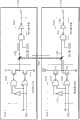
图7示出了根据实施例的读取FIFO控制器710和720。在图7中,为便于说明,下面将描述包括在主芯片110中的读取FIFO控制器710和包括在直接层叠在主芯片110上的第一从芯片120中的读取FIFO控制器720,然而,应当理解的是,3D半导体器件中的所有芯片均可包括FIFO控制器。主芯片110包括读取从存储单元阵列块205输出的数据RD1[3:0]和RD1[7:4](参见图2和4)的数据输入/输出驱动/感测放大器IODRV/IOSA 220。读取数据RD1[3:0]和RD1[7:4]可顺序地(如读取数据RD1[3:0]后紧跟读取数据RD1[7:4])传输到FIFO控制器710。主芯片110还包括:命令缓冲器和命令译码器CMDDEC CMDQ 236,其驱动由读取命令产生的第一对准信号FRP_PDL;计数器700,其响应由主芯片110或第一从芯片120提供的第一对准信号FRP_PDL,产生第三对准信号PDL#[1:0];读取FIFO控制器710,其响应芯片识别信号CID以及第一对准信号FRP_PDL,传输主芯片110的读取数据RD1[3:0]和RD1[7:4]以及第一从芯片120的读取数据RD0[3:0]和RD0[7:4];以及读取FIFO 222,其响应第三对准信号PDL#[1:0],顺序地存储主芯片110的读取数据RD1[3:0]和RD1[7:4]以及第一从芯片120的读取数据RD0[3:0]和RD0[7:4]。FIG. 7 shows readFIFO controllers 710 and 720 according to an embodiment. In FIG. 7, for convenience of explanation, theread FIFO controller 710 included in themaster chip 110 and theread FIFO controller 720 included in thefirst slave chip 120 directly stacked on themaster chip 110 will be described below, However, it should be understood that all chips in a 3D semiconductor device may include a FIFO controller. Themain chip 110 includes a data input/output drive/sense amplifier IODRV/IOSA 220 that reads data RD1[3:0] and RD1[7:4] (see FIGS. 2 and 4 ) output from the memorycell array block 205. The read data RD1[3:0] and RD1[7:4] can be transmitted to theFIFO controller 710 sequentially (eg read data RD1[3:0] followed by read data RD1[7:4]).Master chip 110 also includes: command buffer and commanddecoder CMDDEC CMDQ 236, which drives the first alignment signal FRP_PDL generated by the read command; The first alignment signal FRP_PDL generates the third alignment signal PDL#[1:0]; theread FIFO controller 710 responds to the chip identification signal CID and the first alignment signal FRP_PDL to transmit the read data of themain chip 110 RD1[3:0] and RD1[7:4] and the read data RD0[3:0] and RD0[7:4] of thefirst slave chip 120; and readFIFO 222, which responds to the third alignment signal PDL#[1:0], sequentially store the read data RD1[3:0] and RD1[7:4] of themaster chip 110 and the read data RD0[3:0] and RD0[ of thefirst slave chip 120 7:4].

第一从芯片120可被制造为具有与主芯片110相同的结构。如图4所示,当位于数据输出路径上的TSV连接部160的位置按照第四界面方案Ⅳ设置时,第一从芯片120的读取FIFO 222和放置置在读取FIFO 222之后的电路块(即串行化器SER 224、数据选通输出缓冲器226、数据输出缓冲器228、数据选通焊盘DQS、以及数据输入/输出焊盘DQ)不需要使用。在目前的实施例中,第一从芯片120的读取FIFO控制器720中的第一和第二解多路器(DEMUX)722和724的输出通过第一和第二TSV连接部160a和160b连接到主芯片110的第一和第二DEMUX电路712和714的输出。因此,第一从芯片120的读取FIFO控制器720中的MUX电路728、或门726、以及缓冲器727不需要使用。主芯片110的读取FIFO控制器710中的MUX电路718、或门716、缓冲器717与第一从芯片120共用。Thefirst slave chip 120 may be manufactured to have the same structure as themaster chip 110 . As shown in Figure 4, when the position of theTSV connection portion 160 on the data output path is set according to the fourth interface scheme IV, thefirst read FIFO 222 from thechip 120 and the circuit block placed after the read FIFO 222 (ie serializer SER 224, datastrobe output buffer 226,data output buffer 228, data strobe pad DQS, and data input/output pad DQ) need not be used. In the current embodiment, the outputs of the first and second demultiplexers (DEMUX) 722 and 724 in theread FIFO controller 720 of thefirst slave chip 120 pass through the first and secondTSV connection parts 160a and 160b Outputs of the first andsecond DEMUX circuits 712 and 714 connected to themain chip 110 . Therefore, theMUX circuit 728 , theOR gate 726 , and thebuffer 727 in theread FIFO controller 720 of thefirst slave chip 120 do not need to be used. TheMUX circuit 718 , ORgate 716 , and buffer 717 in theread FIFO controller 710 of themaster chip 110 are shared with thefirst slave chip 120 .

主芯片110的读取FIFO控制器710包括第一和第二DEMUX 712和714、以及MUX718、或门716、以及缓冲器717。第一DEMUX 712包括一个输出端子I以及两个输出端子O1和O2。第一DEMUX电路712的输入端子I输入通过数据输入/输出驱动/感测放大器IODRV/IOSA 220传输的4比特输入数据(如顺序地先输入数据RD1[3:0],然后输入数据RD1[7:4])。第一DEMUX电路712响应主芯片110的芯片识别信号CID,输出4比特输入数据(如读取数据RD1[3:0]和RD1[7:4])到连接到第一信号线702的第一输出端子O1。第一DEMUX电路712的第二输出端子O2连接到第二信号线704。第二信号线704连接到第一TSV连接部160a,用于连接主芯片110和第一从芯片120。例如,主芯片110的芯片识别信号CID可被设置为“0”,以及第一从芯片120的芯片识别信号CID可被设置为“1”。Theread FIFO controller 710 of themain chip 110 includes first andsecond DEMUX 712 and 714, and aMUX 718, an ORgate 716, and abuffer 717. Thefirst DEMUX 712 includes one output terminal I and two output terminals O1 and O2. The input terminal I of thefirst DEMUX circuit 712 inputs the 4-bit input data transmitted by the data input/output drive/sensing amplifier IODRV/IOSA 220 (such as input data RD1[3:0] first in sequence, and then input data RD1[7] :4]). Thefirst DEMUX circuit 712 responds to the chip identification signal CID of themain chip 110, and outputs 4-bit input data (such as read data RD1[3:0] and RD1[7:4]) to the first signal line connected to thefirst signal line 702. Output terminal O1. The second output terminal O2 of thefirst DEMUX circuit 712 is connected to thesecond signal line 704 . Thesecond signal line 704 is connected to the firstTSV connection part 160 a for connecting themaster chip 110 and thefirst slave chip 120 . For example, the chip identification signal CID of themaster chip 110 may be set to '0', and the chip identification signal CID of thefirst slave chip 120 may be set to '1'.

第二信号线704通过第一TSV 160连接到第一从芯片120的第一DEMUX电路722的输出。第一从芯片120的第一DEMUX电路722响应第一从芯片120的芯片识别信号CID,在其输入端子I顺序地输入第一从芯片120的读取数据RD0[3:0]和RD0[7:4],以及顺序地输出读取数据RD0[3:0]和RD0[7:4]到连接到第二信号线723的第二输出端子O2。第一从芯片120的第二信号线723通过第一TSV 160a连接到主芯片110的第二信号线704。因此,第一从芯片120的读取数据RD0[3:0]和RD0[7:4]传输(在这个例子中,顺序地传输)到主芯片110的第二信号线704。Thesecond signal line 704 is connected to the output of thefirst DEMUX circuit 722 of thefirst slave chip 120 through thefirst TSV 160. Thefirst DEMUX circuit 722 of thefirst slave chip 120 responds to the chip identification signal CID of thefirst slave chip 120, and sequentially inputs the read data RD0[3:0] and RD0[7] of thefirst slave chip 120 at itsinput terminal 1. :4], and sequentially output the read data RD0[3:0] and RD0[7:4] to the second output terminal O2 connected to thesecond signal line 723 . Thesecond signal line 723 of thefirst slave chip 120 is connected to thesecond signal line 704 of themaster chip 110 through thefirst TSV 160a. Therefore, the read data RD0[3:0] and RD0[7:4] of thefirst slave chip 120 are transmitted (in this example, sequentially transmitted) to thesecond signal line 704 of themaster chip 110 .

第二DEMUX电路714包括一个输入端子I和两个输出端子O1和O2。第二DEMUX电路714输入第一对准信号FRP_PDL到输入端子I,该信号由命令缓冲器与命令译码器CMDDEC CMDQ 236驱动。第二DEMUX电路714响应主芯片110的芯片识别信号CID,输出第一对准信号FRP_PDL到连接到第三信号线706的第一输出端O1。第二DEMUX电路714的第二输出端子O2连接到第四信号线708。第四信号线708连接到第二TSV 160b,用于连接主芯片110和从芯片120。Thesecond DEMUX circuit 714 includes one input terminal I and two output terminals O1 and O2. Thesecond DEMUX circuit 714 inputs the first alignment signal FRP_PDL to the input terminal I, and the signal is driven by the command buffer and commanddecoder CMDDEC CMDQ 236 . Thesecond DEMUX circuit 714 outputs the first alignment signal FRP_PDL to the first output terminal O1 connected to thethird signal line 706 in response to the chip identification signal CID of themain chip 110 . The second output terminal O2 of thesecond DEMUX circuit 714 is connected to thefourth signal line 708 . Thefourth signal line 708 is connected to thesecond TSV 160b for connecting themaster chip 110 and theslave chip 120.

第四信号线708通过第二TSV连接部160b连接到第一从芯片120的第二DEMUX电路724的输出。第一从芯片120的第二DEMUX电路724响应第一从芯片120的芯片识别信号CID,输入第一从芯片120的第一对准信号FRP_PDL到输入端子I,以及输出第一对准信号FRP_PDL到连接到第四信号线725的第二输出端子O2。第一从芯片120的第四信号线725通过第二TSV连接部160b连接到主芯片110的第四信号线708。因此,第一从芯片120的第一对准信号FRP_PDL传输到主芯片110的第四信号线708。Thefourth signal line 708 is connected to the output of thesecond DEMUX circuit 724 of thefirst slave chip 120 through thesecond TSV connection 160b. Thesecond DEMUX circuit 724 of thefirst slave chip 120 responds to the chip identification signal CID of thefirst slave chip 120, inputs the first alignment signal FRP_PDL of thefirst slave chip 120 to the input terminal I, and outputs the first alignment signal FRP_PDL to Connected to the second output terminal O2 of thefourth signal line 725 . Thefourth signal line 725 of thefirst slave chip 120 is connected to thefourth signal line 708 of themaster chip 110 through the secondTSV connection part 160b. Therefore, the first alignment signal FRP_PDL of thefirst slave chip 120 is transmitted to thefourth signal line 708 of themaster chip 110 .

主芯片110的第一对准信号FRP_PDL传输到的第三信号线706以及第一从芯片120的第一对准信号FRP_PDL传输到的第四信号线708连接到或门716。或门716的输出,即来自主芯片110和第一从芯片120的FRP_PDL信号的逻辑或操作的结果信号FRP_PDLD,被传输到逻辑电路717。逻辑电路717响应FRP_PDLD产生第二对准信号FRP_QCTRL,其包含主芯片110的第一对准信号FRP_PDL和第一从芯片120的第一对准信号FRP_PDL的信息。并且,从或门716输出的信号FRP_PDLD提供到计数器700,并且其产生第三对准信号PDL#[1:0],用于将主芯片110的读取数据RD1[3:0]和RD1[7:4]和第一从芯片120的读取数据RD0[3:0]和RD0[7:4]顺序地存储在读取FIFO222中。Thethird signal line 706 to which the first alignment signal FRP_PDL of themaster chip 110 is transmitted and thefourth signal line 708 to which the first alignment signal FRP_PDL of thefirst slave chip 120 is transmitted are connected to theOR gate 716 . The output of theOR gate 716 , that is, the resultant signal FRP_PDLD of the logical OR operation of the FRP_PDL signals from themaster chip 110 and thefirst slave chip 120 is transmitted to thelogic circuit 717 . Thelogic circuit 717 generates the second alignment signal FRP_QCTRL in response to the FRP_PDLD, which includes the information of the first alignment signal FRP_PDL of themaster chip 110 and the first alignment signal FRP_PDL of thefirst slave chip 120 . And, the signal FRP_PDLD output from theOR gate 716 is provided to thecounter 700, and it generates a third alignment signal PDL#[1:0] for aligning the read data RD1[3:0] and RD1[ 7:4] and the read data RD0[3:0] and RD0[7:4] of thefirst slave chip 120 are sequentially stored in theread FIFO 222 .

MUX电路718包括两个输入端子I1和I2以及一个输出端子O。在MUX电路718中,主芯片110的读取数据RD1[3:0]和RD1[7:4]传输到的第一信号线702连接到第一输入端子I1、以及第一从芯片120的读取数据RD0[3:0]和RD0[7:4]传输到的第二信号线704连接到第二输入端子I2。MUX电路718响应第二对准信号FRP_QCTRL,输出主芯片110的读取数据RD1[3:0]和RD1[7:4]以及第一从芯片120的读取数据RD0[3:0]和RD0[7:4]到输出端子O,其中这些读取数据输入到第一和第二输入端子I1和I2。MUX电路718的输出端子O连接到读取FIFO 222。TheMUX circuit 718 includes two input terminals I1 and I2 and one output terminal O. In theMUX circuit 718, thefirst signal line 702 to which the read data RD1[3:0] and RD1[7:4] of themaster chip 110 are transmitted is connected to the first input terminal I1, and the read data of thefirst slave chip 120 Thesecond signal line 704 to which the data RD0[3:0] and RD0[7:4] are transmitted is connected to the second input terminal I2. TheMUX circuit 718 responds to the second alignment signal FRP_QCTRL, and outputs the read data RD1[3:0] and RD1[7:4] of themaster chip 110 and the read data RD0[3:0] and RD0 of the first slave chip 120 [7:4] to the output terminal O, where these read data are input to the first and second input terminals I1 and I2. Output terminal O ofMUX circuit 718 is connected to readFIFO 222.

读取FIFO 222响应第三对准信号PDL#[1:0],顺序地存储第一从芯片120的读取数据RD1[3:0]和RD1[7:4]以及主芯片110的读取数据RD0[3:0]和RD0[7:4]。响应FIFO输出控制信号EXTCLK#(DOI<3:0>),顺序输出存储在读取FIFO 222中的主芯片110的读取数据RD1[3:0]和RD1[7:4]和第一从芯片120的读取数据RD0[3:0]和RD0[7:4]。Theread FIFO 222 responds to the third alignment signal PDL#[1:0], and sequentially stores the read data RD1[3:0] and RD1[7:4] of thefirst slave chip 120 and the read data of themaster chip 110. Data RD0[3:0] and RD0[7:4]. In response to the FIFO output control signal EXTCLK#(DOI<3:0>), sequential output is stored in the read data RD1[3:0] and RD1[7:4] of themain chip 110 in theread FIFO 222 and the first slave The read data RD0[3:0] and RD0[7:4] of thechip 120 .

即使第一从芯片120的读取数据RD0[3:0]和RD0[7:4]到达主芯片110的延迟时间与主芯片110的读取数据RD1[3:0]和RD1[7:4]的延迟时间不同,主芯片110的读取FIFO控制器710的MUX电路718也会选择性地传输第一从芯片120的读取数据RD0[3:0]和RD0[7:4]和主芯片110的读取数据RD1[3:0]和RD1[7:4]到读取FIFO 222。电流灼伤(burn)现象可以避免。下面参考附图8来描述电流灼伤现象,其中附图8示出如图7所示的主芯片110和第一从芯片120的可选实施例。Even if the read data RD0[3:0] and RD0[7:4] of thefirst slave chip 120 arrive at the delay time of themaster chip 110 and the read data RD1[3:0] and RD1[7:4] of the master chip 110 ] delay time is different, theMUX circuit 718 of theread FIFO controller 710 of themaster chip 110 will also selectively transmit the read data RD0[3:0] and RD0[7:4] of thefirst slave chip 120 and the master The read data RD1[3:0] and RD1[7:4] of thechip 110 are sent to theread FIFO 222. Electric burn (burn) phenomenon can be avoided. The current burning phenomenon will be described below with reference to FIG. 8 , which shows an alternative embodiment of themaster chip 110 and thefirst slave chip 120 as shown in FIG. 7 .

图8示出了在FIFO 222中存储数据的可选实施例,其中响应于第一使能(enable)信号TSVEN_M,主芯片110的读取数据RD1[3:0]和RD1[7:4]通过第一三态缓冲器810传输到第一信号线802。该第一使能信号TSVEN_M在主芯片110中产生。响应于第二使能信号TSVEN_S,第一从芯片120的读取数据RD0[3:0]和RD0[7:4]通过第二三态缓冲器820传输到第二信号线822。该第二使能信号TSVEN_S在第一从芯片120中产生。第二信号线822通过TSV160c而连接到第一信号线802。第一从芯片120的读取数据RD0[3:0]和RD0[7:4]通过TSV 160c传输到第一信号线802。传输到第一信号线802的主芯片110的读取数据RD1[3:0]和RD1[7:4]以及第一从芯片120的读取数据RD0[3:0]和RD0[7:4]被顺序地存储在读取FIFO222中,然后被输出。FIG. 8 shows an optional embodiment of storing data in theFIFO 222, wherein in response to the first enable (enable) signal TSVEN_M, the read data RD1[3:0] and RD1[7:4] of themain chip 110 It is transmitted to thefirst signal line 802 through the firsttri-state buffer 810 . The first enable signal TSVEN_M is generated in themain chip 110 . In response to the second enable signal TSVEN_S, the read data RD0[3:0] and RD0[7:4] of thefirst slave chip 120 are transmitted to thesecond signal line 822 through the secondtri-state buffer 820 . The second enable signal TSVEN_S is generated in thefirst slave chip 120 . Thesecond signal line 822 is connected to thefirst signal line 802 through theTSV 160c. The read data RD0[3:0] and RD0[7:4] of thefirst slave chip 120 are transmitted to thefirst signal line 802 through theTSV 160c. The read data RD1[3:0] and RD1[7:4] of themaster chip 110 transmitted to thefirst signal line 802 and the read data RD0[3:0] and RD0[7:4] of the first slave chip 120 ] are sequentially stored in theread FIFO 222, and then output.

由于在半导体制造过程中主芯片110和第一从芯片120的变化因素,主芯片110的读取数据RD1[3:0]和RD1[7:4]到达读取FIFO 222的时间以及第一从芯片120的读取数据RD0[3:0]和RD0[7:4]到达读取FIFO 222的时间彼此之间会不同。当主芯片110的读取数据RD1[3:0]和RD1[7:4]和第一从芯片120的读取数据RD0[3:0]和RD0[7:4]的无缝数据输出操作进行时,会在第一信号线802、TSV160、以及第二信号线822中发生读取数据冲突。例如,第一从芯片120的读取数据RD0[3:0]和RD0[7:4]为逻辑高电平并且主芯片110的读取数据RD1[3:0]和RD1[7:4]为逻辑低电平,在第二三态缓冲器820、第一信号线802、TSV160、以及第一三态缓冲器810之间形成电流路径800。由于该电流路径800的存在,会发生电流灼伤现象。Due to the variable factors of themaster chip 110 and thefirst slave chip 120 in the semiconductor manufacturing process, the time when the read data RD1[3:0] and RD1[7:4] of themaster chip 110 arrive at theread FIFO 222 and the first slave The times when the read data RD0[3:0] and RD0[7:4] of thechip 120 arrive at theread FIFO 222 are different from each other. When the seamless data output operation of the read data RD1[3:0] and RD1[7:4] of themaster chip 110 and the read data RD0[3:0] and RD0[7:4] of thefirst slave chip 120 is performed , read data conflicts may occur in thefirst signal line 802 , theTSV 160 , and thesecond signal line 822 . For example, the read data RD0[3:0] and RD0[7:4] of thefirst slave chip 120 are logic high level and the read data RD1[3:0] and RD1[7:4] of themaster chip 110 For a logic low level, acurrent path 800 is formed between the secondtri-state buffer 820 , thefirst signal line 802 , theTSV 160 , and the firsttri-state buffer 810 . Due to the existence of thecurrent path 800 , current burn occurs.

当无缝数据输出操作进行时发生的该电流灼伤现象可通过读取FIFO控制器710避免,该控制器710控制读取FIFO 222通过分别独立的第一和第二信号线702和704将第一从芯片120的读取数据RD0[3:0]和RD0[7:4]以及主芯片110的读取数据RD1[3:0]和RD1[7:4]传输到主芯片110,并且控制MUX电路718选择性地传输第一从芯片120的读取数据RD0[3:0]和RD0[7:4]以及主芯片110的读取数据RD1[3:0]和RD1[7:4]到读取FIFO 222。This current burn phenomenon that occurs when a seamless data output operation is in progress can be avoided by theread FIFO controller 710, which controls theread FIFO 222 to transfer the first The read data RD0[3:0] and RD0[7:4] of theslave chip 120 and the read data RD1[3:0] and RD1[7:4] of themaster chip 110 are transmitted to themaster chip 110, and control the MUX Thecircuit 718 selectively transmits the read data RD0[3:0] and RD0[7:4] of thefirst slave chip 120 and the read data RD1[3:0] and RD1[7:4] of themaster chip 110 to ReadFIFO 222.

响应于在主芯片110和第一从芯片120中产生的第一和第二使能信号TSVEN_M和TSVEN_S,如图8所示的第一和第二三态缓冲器810和820的每一个均驱动主芯片110的读取数据RD1[3:0]和RD1[7:4]以及第一从芯片120的读取数据RD0[3:0]和RD0[7:4]。另一方面,响应于主芯片110和第一从芯片120中每一个的芯片识别信号CID,如图7所示的读取FIFO控制器710和720选择性地传输第一从芯片120的读取数据RD0[3:0]和RD0[7:4]以及主芯片110的读取数据RD1[3:0]和RD1[7:4]。因此,如图7所示的主芯片110和第一从芯片120不需要额外的电路块来产生第一和第二使能信号TSVEN_M和TSVEN_S。In response to the first and second enable signals TSVEN_M and TSVEN_S generated in themaster chip 110 and thefirst slave chip 120, each of the first and secondtri-state buffers 810 and 820 shown in FIG. The read data RD1[3:0] and RD1[7:4] of themaster chip 110 and the read data RD0[3:0] and RD0[7:4] of thefirst slave chip 120 . On the other hand, in response to the chip identification signal CID of each of themaster chip 110 and thefirst slave chip 120, theread FIFO controllers 710 and 720 shown in FIG. The data RD0[3:0] and RD0[7:4] and the read data RD1[3:0] and RD1[7:4] of themaster chip 110 . Therefore, themaster chip 110 and thefirst slave chip 120 shown in FIG. 7 do not require additional circuit blocks to generate the first and second enable signals TSVEN_M and TSVEN_S.

图9示出了上面描述的3D半导体器件100的如图7所示的读取FIFO控制器710和720的操作时序图。参考图9,提供第一从芯片120的读取数据RD0[3:0]和RD0[7:4]和第一对准信号FRDTP,以及提供主芯片110的读取数据RD1[3:0]和RD1[7:4]和第一对准信号FRDTP。第一从芯片120的读取数据RD0[3:0]和RD0[7:4]传输到主芯片110的第二信号线704,以及主芯片110的读取数据RD1[3:0]和RD1[7:4]传输到主芯片110的第一信号线702。信号FRP_PDLD由第一从芯片120和主芯片110的FRDTP信号的逻辑或操作而产生。第二对准信号FRP_QCTRL由逻辑电路717响应信号FRP_PDLD而产生。响应于用于选择多路器718的输入的第二对准信号FRP_QCTRL,第一从芯片120的读取数据RD1[3:0]和RD1[7:4]以及主芯片110的读取数据RD0[3:0]和RD0[7:4]传输到读取FIFO 222。读取FIFO 222响应第三对准信号PDL#[1:0],顺序地存储第一从芯片120的读取数据RD1[3:0]和RD1[7:4]以及主芯片110的读取数据RD0[3:0]和RD0[7:4]。响应于FIFO输出控制信号EXTCLK#DOI<3:0>),顺序地输出存储在读取FIFO 222中的第一从芯片120的读取数据RD1[3:0]和RD1[7:4]以及主芯片110的读取数据RD0[3:0]和RD0[7:4]。FIG. 9 shows an operation timing diagram of the readFIFO controllers 710 and 720 shown in FIG. 7 of the3D semiconductor device 100 described above. Referring to FIG. 9 , the read data RD0[3:0] and RD0[7:4] of thefirst slave chip 120 and the first alignment signal FRDTP are provided, and the read data RD1[3:0] of themaster chip 110 are provided. and RD1[7:4] and the first alignment signal FRDTP. The read data RD0[3:0] and RD0[7:4] of thefirst slave chip 120 are transmitted to thesecond signal line 704 of themaster chip 110, and the read data RD1[3:0] and RD1 of the master chip 110 [7:4] transmitted to thefirst signal line 702 of themain chip 110 . The signal FRP_PDLD is generated by the logical OR operation of the FRDTP signals of thefirst slave chip 120 and themaster chip 110 . The second alignment signal FRP_QCTRL is generated by thelogic circuit 717 in response to the signal FRP_PDLD. In response to the second alignment signal FRP_QCTRL for selecting the input of themultiplexer 718, the read data RD1[3:0] and RD1[7:4] of thefirst slave chip 120 and the read data RD0 of the master chip 110 [3:0] and RD0[7:4] are transferred to theread FIFO 222. Theread FIFO 222 responds to the third alignment signal PDL#[1:0], and sequentially stores the read data RD1[3:0] and RD1[7:4] of thefirst slave chip 120 and the read data of themaster chip 110. Data RD0[3:0] and RD0[7:4]. In response to the FIFO output control signal EXTCLK#DOI<3:0>), sequentially output the read data RD1[3:0] and RD1[7:4] and RD1[7:4] of thefirst slave chip 120 stored in theread FIFO 222 and Read data RD0[3:0] and RD0[7:4] of themaster chip 110 .

如上所述,图7示出了包括主芯片110和单个从芯片(第一从芯片120)的3D半导体器件100的例子。当需要附加从芯片时,如图7所示的TSV连接部160可被扩展用于附加从芯片,从而使得TSV连接部160a和160b与附加从芯片所共用。可选地,对于增加的每个附加从芯片,可为主芯片110增加专用信号线以作为到多路器718的附加输入(类似于主芯片的信号线704),以及增加专用信号线作为到或门716的附加输入(类似于主芯片的信号线708),两个附加TSV连接部160(类似于TSV连接部160a和160b)从主芯片110中的这些附加专用信号线延伸到附加从芯片的信号线723和725。将会认识到的是,主芯片110的其它电路应当变型以适应这样的变化,包括如多路器718和或门716的变型以适应这些附加输入。As described above, FIG. 7 shows an example of the3D semiconductor device 100 including themaster chip 110 and a single slave chip (first slave chip 120 ). When an additional slave chip is required, theTSV connection 160 shown in FIG. 7 can be extended for the additional slave chip, so that theTSV connection 160a and 160b are shared with the additional slave chip. Optionally, for each additional slave chip that is added, a dedicated signal line can be added to themaster chip 110 as an additional input to the multiplexer 718 (similar to thesignal line 704 of the master chip), and a dedicated signal line can be added as a signal line to the Additional input of OR gate 716 (similar to signalline 708 of master chip), two additional TSV connections 160 (similar toTSV connections 160a and 160b) extend from these additional dedicated signal lines inmaster chip 110 to additional slave chips signallines 723 and 725. It will be appreciated that other circuitry of themaster chip 110 should be modified to accommodate such changes, including modifications such asmultiplexer 718 andOR gate 716 to accommodate these additional inputs.

作为进一步的例子,从芯片可被分为共用TSV连接部160的多个组。例如,第一TSV连接部160可专用于将第一组从芯片连接到主芯片110,以及第二TSV连接部160可专用于将第二组从芯片连接到主芯片110。进一步的,共用这些TSV连接部160的从芯片可被选定(或给定芯片ID(CID)或进行编程),从而使得同一组中的从芯片彼此之间不会顺序地输出数据。例如,第一组从芯片输出到它们的相应共用第一TSV连接部160的FIFO控制器的数据输出(如专用于第一组)与第二组从芯片输出到它们的相应共用第二TSV连接部的FIFO控制器的数据输出(如专用于第二组)可在时间上交替。例如,第一组从芯片可在时间t0、t2、t4和t6时输出数据到它们各自的FIFO控制器,而第二组从芯片可在时间t1、t3和t5时(并且主芯片可在时间t7时输出数据到FIFO 710)输出数据到FIFO控制器。通过分开使用TSV连接部160,电流灼伤的风险可降低并同时减小电路尺寸。As a further example, slave chips may be divided into groups that share theTSV connection 160 . For example, thefirst TSV connection 160 may be dedicated to connecting the first set of slave chips to themaster chip 110 , and thesecond TSV connection 160 may be dedicated to connecting the second set of slave chips to themaster chip 110 . Further, the slave chips that share theseTSV connections 160 can be selected (or given a chip ID (CID) or programmed) so that the slave chips in the same group do not output data sequentially with each other. For example, the data outputs of a first set of slave chips output to their respective FIFO controllers of the common first TSV connection 160 (eg, dedicated to the first set) are the same as those of the second set of slave chips output to their respective common second TSV connections. The data output of the first FIFO controller (eg dedicated to the second group) can be alternated in time. For example, a first group of slave chips may output data to their respective FIFO controllers at times t0, t2, t4, and t6, while a second group of slave chips may be at times t1, t3, and t5 (and the master chip may be at time Output data to FIFO 710) output data to FIFO controller during t7. By using theTSV connections 160 separately, the risk of electric current burns can be reduced and at the same time reduce the size of the circuit.

图10示出了如图1所示的3D半导体器件100的全局控制操作。参考图10,层叠在如图1所示的3D半导体器件100中的主芯片110和第一到第三从芯片120、130和140的每一个均可具有与上面描述的图2所示的半导体存储器件200相同的电路设计。3D半导体器件100包括多个层阶,这些层阶包括主芯片110和第一到第三从芯片120、130和140。该多个层阶可被限定为一组DRAM芯片,其中相同的命令焊盘CMD和地址焊盘ADDR被输入到该组DRAM芯片。一般地,这些层阶通过芯片选择信号CS来区分。例如,作为第一层阶的主芯片110由第一芯片选择信号CS0所驱动,作为第二层阶的第一从芯片120由第二芯片选择信号CS1所驱动,作为第三层阶的第二从芯片130由第三芯片选择信号CS2所驱动,作为第四层阶的第三从芯片140由第四芯片选择信号CS3所驱动。芯片选择信号CS0、CS1、CS2和CS3可施加到命令焊盘CMD或其它焊盘,如现有技术中已知的那样。此外,芯片选择信号施加的方式可与命令通过命令焊盘CMD施加的方式类似,例如可提供独立的芯片选择焊盘,并且硅贯通孔连接部可通过这里针对主和从芯片的命令与命令路径所描述的方式将主芯片的芯片选择路径连接到从芯片的芯片选择路径。FIG. 10 shows global control operations of the3D semiconductor device 100 shown in FIG. 1 . Referring to FIG. 10, each of themaster chip 110 and the first tothird slave chips 120, 130, and 140 stacked in the3D semiconductor device 100 shown in FIG. Thememory device 200 has the same circuit design. The3D semiconductor device 100 includes a plurality of levels including amaster chip 110 and first tothird slave chips 120 , 130 and 140 . The plurality of hierarchies may be defined as a group of DRAM chips to which the same command pad CMD and address pad ADDR are input. Generally, these levels are distinguished by a chip select signal CS. For example, themaster chip 110 of the first level is driven by the first chip selection signal CS0, thefirst slave chip 120 of the second level is driven by the second chip selection signal CS1, and the second chip of the third level is driven by the second chip selection signal CS1. Theslave chip 130 is driven by the third chip select signal CS2, and thethird slave chip 140 as the fourth level is driven by the fourth chip select signal CS3. Chip select signals CS0, CS1, CS2, and CS3 may be applied to command pad CMD or other pads, as is known in the art. In addition, the chip select signal can be applied in a manner similar to the command applied through the command pad CMD, for example, a separate chip select pad can be provided, and the TSV connection can pass through the command and command paths for the master and slave chips. The described way connects the chip-select path of the master chip to the chip-select path of the slave chip.

当所有的主芯片110和第一到第三从芯片120、130和140一起操作时,控制主芯片110和第一到第三从芯片120、130和140的逻辑电路被放置在主芯片110中。例如,当TSV连接部160位于数据输出路径上的位置按照第四界面方案Ⅳ设定时(如参见附图4),延迟同步电路DLL260、延迟控制器262、读取FIFO 222、串行化器SER 224、以及数据输入/输出、命令和地址相关逻辑电路构成全局控制电路1000,其控制主芯片110和第一到第三从芯片120、130和140的数据输出。即使读取操作在第一到第四层阶中一个层阶的任一芯片中进行时(如读取操作在主芯片110和第一到第三从芯片120、130和140中的任一芯片中进行),主芯片110中的全局控制电路1000也可正常工作。When all themaster chip 110 and the first tothird slave chips 120, 130 and 140 are operated together, the logic circuits controlling themaster chip 110 and the first tothird slave chips 120, 130 and 140 are placed in themaster chip 110 . For example, when the position of theTSV connection part 160 on the data output path is set according to the fourth interface scheme IV (as referring to accompanying drawing 4), the delay synchronous circuit DLL260,delay controller 262, readFIFO 222, serializer TheSER 224, and data input/output, command and address related logic circuits constitute theglobal control circuit 1000, which controls the data output of themaster chip 110 and the first tothird slave chips 120, 130 and 140. Even when the read operation is performed in any chip of one of the first to fourth levels (for example, the read operation is performed in any chip of themaster chip 110 and the first tothird slave chips 120, 130, and 140 ), theglobal control circuit 1000 in themain chip 110 can also work normally.

图10还示出了实现根据图3、4、5和6描述的几个TSV连接部界面可选方案的示例性TSV界面1010。具体来说,在图10的例子中,数据输入路径的TSV连接部按照方案Ⅱ(如根据附图3描述的那样)设置,使得到数据输入路径的TSV连接部160a位于数据输入缓冲器210与触发器213之间的对应位置处。在图10的例子中,数据输出路径的TSV连接部界面按照方案Ⅳ(如根据图4描述的那样)设置,到数据输出路径的TSV连接部160b位于数据输入/输出驱动/感测放大器IODRV/IOSA 220与FIFO 222之间的对应位置处。命令/地址路径的TSV连接部界面按照方案Ⅱ(如根据图5讨论的那样)设置,到命令路径和地址路径的TSV连接部160c分别地设置在命令输入缓冲器232与触发器234之间以及在地址输入缓冲器230与触发器233之间。时钟输出路径的TSV连接部界面按照方案Ⅱ(如根据图6讨论的那样)设置,到时钟路径的TSV连接部160d设置在时钟输入缓冲器240与时钟发生器和缓冲器电路CLK 242之间。TSV界面在图10中由粗虚线1010表示。TSV连接部160I、160m、160n、160o、160p和160q在图10中由点斜线(dotwith a slash)表示,其中每个点斜线为表示一个或多个TSV连接部160的符号,TSV连接部的数量取决于芯片间要连接的信号线数量(例如,如果连接部是到4比特宽内部数据总线,则一个TSV连接部符号表示分别将一个芯片的4比特宽数据总线的每个信号线连接到其它芯片的对应信号线的4个TSV连接部160)。应当注意的是,图10中的TSV连接部参考标记160I、160m、160n、160o、160p和160q并不意味着这些TSV连接部必须要与本应用中描述的其它TSV连接部不同-它们可以是相同或不同的,这将是很清楚的。例如,尽管TSV连接部160n具有与参考图7和8描述的TSV连接部160a和160c不同的参考标记,但是TSV连接部160n也可表示TSV连接部160a和/或160c。FIG. 10 also shows anexemplary TSV interface 1010 implementing several TSV connector interface options described with respect to FIGS. 3 , 4 , 5 and 6 . Specifically, in the example of FIG. 10 , the TSV connection portion of the data input path is arranged according to scheme II (as described with reference to FIG. 3 ), so that theTSV connection portion 160a to the data input path is located between thedata input buffer 210 and The corresponding positions betweentriggers 213. In the example of FIG. 10, the TSV connection portion interface of the data output path is arranged according to scheme IV (as described with reference to FIG. 4), and theTSV connection portion 160b to the data output path is located at the data input/output drive/sense amplifier IODRV/ The corresponding position betweenIOSA 220 andFIFO 222. The TSV connector interface for the command/address path is arranged according to Scheme II (as discussed with respect to FIG. Between addressinput buffer 230 and flip-flop 233 . The TSV connection interface of the clock output path is arranged according to scheme II (as discussed with respect to FIG. 6 ), theTSV connection 160d to the clock path is arranged between theclock input buffer 240 and the clock generator andbuffer circuit CLK 242. The TSV interface is represented by a bold dashedline 1010 in FIG. 10 .TSV connection portions 160I, 160m, 160n, 160o, 160p, and 160q are represented by dot with a slash in FIG. The number of sections depends on the number of signal lines to be connected between chips (for example, if the connection section is to a 4-bit wide internal data bus, a TSV connection section symbol represents connecting each signal line of a chip's 4-bitwide data bus 4TSV connections 160 connected to corresponding signal lines of other chips). It should be noted that the TSV connections referenced 160I, 160m, 160n, 160o, 160p and 160q in FIG. Same or different, it will be clear. For example, although the TSV connection part 160n has a different reference numeral from theTSV connection parts 160a and 160c described with reference to FIGS.

图11示出了用于控制如图10所示的全局控制电路1000的全局芯片选择信号发生电路。为了便于说明,图11将描述全局芯片选择信号发生电路1110和1120,它们可被包括在主芯片110和直接地层叠在主芯片110上的第一从芯片120中。主芯片110的全局芯片选择信号发生电路1110包括:第一与门1112,其输入在主芯片110的芯片识别熔丝(fuse)单元1111中产生的芯片识别信号CID的反相值与第一芯片选择信号CS0;第二与门1113,其输入主芯片110的芯片识别信号CID以及第二芯片选择信号CS1;以及第一或门1114,其输入第一和第二与门1112和1113的输出。在这个例子中,为0的芯片ID(CID=0)设置该芯片作为主芯片。通过设定芯片ID为0,输入到与门1112的反相芯片ID将被设定为1,使得输入到与门1112的CS0通过与门1112到或门1114,并且输入到与门1113的芯片ID将被设定为0,从而使得与门1113输出0。因此,第一或门1114的逻辑输出与CS0逻辑是相同的。或门1114的输出可用于芯片的芯片选择(CS_ME)。因此,CS0可用于选择主芯片110,使得其芯片ID CID设定为0。主芯片110响应其自身的芯片选择信号CS_ME来操作。FIG. 11 shows a global chip select signal generation circuit for controlling theglobal control circuit 1000 shown in FIG. 10 . For convenience of explanation, FIG. 11 will describe global chip selectionsignal generation circuits 1110 and 1120 , which may be included in themaster chip 110 and thefirst slave chip 120 directly stacked on themaster chip 110 . The global chip selectionsignal generating circuit 1110 of themain chip 110 includes: a first ANDgate 1112, which inputs the inversion value of the chip identification signal CID generated in the chip identification fuse (fuse)unit 1111 of themain chip 110 and the first chip the selection signal CS0; the second ANDgate 1113, which inputs the chip identification signal CID of themain chip 110 and the second chip selection signal CS1; and the first ORgate 1114, which inputs the outputs of the first and second ANDgates 1112 and 1113. In this example, a chip ID of 0 (CID=0) sets the chip as the master chip. By setting the chip ID to 0, the inverted chip ID input to the ANDgate 1112 will be set to 1, so that the CS0 input to the ANDgate 1112 passes through the ANDgate 1112 to theOR gate 1114, and is input to the chip of the ANDgate 1113 ID will be set to 0, causing ANDgate 1113 tooutput 0. Therefore, the logic output of the first ORgate 1114 is the same as CS0 logic. The output ofOR gate 1114 can be used for chip select (CS_ME) of the chip. Therefore, CS0 can be used to select themaster chip 110 such that its chip ID CID is set to 0. Themaster chip 110 operates in response to its own chip select signal CS_ME.

主芯片110的全局芯片选择信号发生电路1110包括:第三与门1115,其输入芯片识别信号CID以及第一芯片选择信号CS0;第四与门1116,其输入主芯片110的芯片识别信号CID的反相信号与第二芯片选择信号CS1;以及第二或门。主芯片110为0的芯片ID(CID=0)使得输入到与门1116的反相芯片ID为1,使得输入到与门1116的CS1通过与门1116到达或门1117。输入到与门1115的为0的芯片ID使得与门1115的输出为0。因此,或门1117的逻辑输出与CS1逻辑相同,并且可被主芯片110利用从而识别从芯片存取请求(CS_OTHER)。The global chip selectionsignal generating circuit 1110 of themain chip 110 includes: a third ANDgate 1115, which inputs the chip identification signal CID and the first chip selection signal CS0; a fourth ANDgate 1116, which inputs the chip identification signal CID of themain chip 110 an inverted signal and a second chip select signal CS1; and a second OR gate. The chip ID of themain chip 110 is 0 (CID=0), so that the inverted chip ID input to the ANDgate 1116 is 1, so that CS1 input to the ANDgate 1116 reaches theOR gate 1117 through the ANDgate 1116 . A chip ID of 0 input to the ANDgate 1115 causes the output of the ANDgate 1115 to be 0. Therefore, the logic output of theOR gate 1117 is the same logic as CS1, and can be utilized by themaster chip 110 to recognize the slave chip access request (CS_OTHER).

芯片选择信号CS_ME和其它芯片选择信号CS_OTHER输入到第三或门1118,并且第三或门1118的输出被生成为全部芯片选择信号CS_ALL。当主芯片110或第一从芯片120被选择时,该全部芯片选择信号CS_ALL被激活。当主芯片110或第一从芯片120操作时,该全部芯片选择信号CS_ALL可用于激活如图10所示的全局控制电路1000,从而使得可进行主芯片110和第一从芯片120中的读取操作。The chip selection signal CS_ME and other chip selection signals CS_OTHER are input to the third ORgate 1118, and the output of the third ORgate 1118 is generated as the all chip selection signal CS_ALL. The all chip select signal CS_ALL is activated when themaster chip 110 or thefirst slave chip 120 is selected. When themaster chip 110 or thefirst slave chip 120 is operating, the all chip select signal CS_ALL can be used to activate theglobal control circuit 1000 shown in FIG. .

在这个例子中,第一从芯片120的全局芯片选择信号发生电路1120具有与主芯片110的全局芯片选择信号发生电路1110相同的结构。唯一的区别在于主芯片110的芯片识别信号CID被设定为“0”,第一从芯片120的芯片识别信号CID被设定为“1”。在主芯片110的芯片识别熔丝单元1111中产生的芯片识别信号CID可在主芯片110中被设定为逻辑“0”。在第一从芯片120的芯片识别熔丝单元1121中产生的芯片识别信号CID可在第一从芯片120中被设定为逻辑“1”。从芯片120的芯片选择信号CS_ME表示第一从芯片120已被选择并操作。从芯片120的其它芯片选择信号CS_OTHER表示第一从芯片120之外(这里指主芯片110)的其它芯片已被选择。第一从芯片120的全部芯片选择信号CS_ALL表示该从芯片之外的其它芯片(这里指主芯片110)和/或第一从芯片120已被选择。不需要使用第一从芯片120的全部芯片选择信号CS_ALL。在该例子中,芯片识别信号CID由芯片识别熔丝单元1111产生。然而,其它的电路也可用于产生芯片识别信号CID,如可由外部命令编程的模式寄存器装置产生。该芯片识别信号CID还可由状态控制信息产生。还应当注意的是,芯片识别熔丝单元1111是可编程的,如由激光熔丝切割操作或由电气熔丝设置操作来编程。此外,如在本申请中使用的那样,应用到产生芯片识别信号CID的电路的限定词“可编程”意于包括可预先编程和/或已编程的元件,尽管对器件的随后修改会阻止进一步的编程。In this example, the global chip selectionsignal generation circuit 1120 of thefirst slave chip 120 has the same structure as the global chip selectionsignal generation circuit 1110 of themaster chip 110 . The only difference is that the chip identification signal CID of themaster chip 110 is set to "0", and the chip identification signal CID of thefirst slave chip 120 is set to "1". The chip identification signal CID generated in the chipidentification fuse unit 1111 of themain chip 110 may be set to logic '0' in themain chip 110 . The chip identification signal CID generated in the chipidentification fuse unit 1121 of thefirst slave chip 120 may be set to logic '1' in thefirst slave chip 120 . The chip select signal CS_ME of theslave chip 120 indicates that thefirst slave chip 120 has been selected and operated. The other chip selection signal CS_OTHER of theslave chip 120 indicates that other chips other than the first slave chip 120 (here, the master chip 110 ) have been selected. The all chip selection signal CS_ALL of thefirst slave chip 120 indicates that other chips (here, the master chip 110 ) and/or thefirst slave chip 120 have been selected. All chip select signals CS_ALL of thefirst slave chip 120 do not need to be used. In this example, the chip identification signal CID is generated by the chipidentification fuse unit 1111 . However, other circuits can also be used to generate the chip identification signal CID, such as a mode register device which can be programmed by an external command. The chip identification signal CID can also be generated by state control information. It should also be noted that the chipidentification fuse unit 1111 is programmable, such as by a laser fuse cutting operation or by an electrical fuse setting operation. Furthermore, as used in this application, the qualifier "programmable" applied to circuitry that generates the chip identification signal CID is intended to include preprogrammable and/or programmed elements, although subsequent modification of the device would prevent further programming.

图12示出了根据一个实施例的全局命令发生器。为了便于说明,图12将描述包括在主芯片110和直接地层叠在主芯片110上第一从芯片120内的全局命令发生电路1210和1220。主芯片110的全局命令发生电路1210和1220包括第一和第二芯片选择信号焊盘1211和1212、第一到第四缓冲器1213、1214、1215和1216、第一和第二锁存器1217和1218、以及命令译码器236。Figure 12 illustrates a global command generator according to one embodiment. For convenience of explanation, FIG. 12 will describe the globalcommand generation circuits 1210 and 1220 included in themaster chip 110 and thefirst slave chip 120 directly stacked on themaster chip 110 . The globalcommand generation circuits 1210 and 1220 of themain chip 110 include first and second chipselection signal pads 1211 and 1212, first tofourth buffers 1213, 1214, 1215 and 1216, first andsecond latches 1217 And 1218, andcommand decoder 236.

输入到主芯片110的第一芯片选择信号焊盘1211的第一芯片选择信号/CS0通过第一和第二缓冲器1213和1214连接到第一信号线1201,以及输入到主芯片110的第二芯片选择信号焊盘1212的第二芯片选择信号/CS1通过第三和第四缓冲器1215和1216连接到第二信号线1202。传输到第一信号线1201的第一芯片选择信号/CS0被存储在响应于主芯片110的内部时钟信号PCLKF的第一锁存器1217中,然后提供给命令译码器CMDDEC 236。传输到第二信号线1202的第二芯片选择信号/CS1被存储在响应于主芯片110的内部时钟信号PCLKF的第二锁存器1218中,然后提供给命令译码器CMDDEC 236。The first chip select signal /CS0 input to the first chipselect signal pad 1211 of themain chip 110 is connected to thefirst signal line 1201 through the first andsecond buffers 1213 and 1214, and thesecond signal line 1201 input to themain chip 110. The second chip selection signal /CS1 of the chipselection signal pad 1212 is connected to thesecond signal line 1202 through the third andfourth buffers 1215 and 1216 . The first chip select signal /CS0 transmitted to thefirst signal line 1201 is stored in thefirst latch 1217 responsive to the internal clock signal PCLKF of themaster chip 110, and then supplied to thecommand decoder CMDDEC 236. The second chip select signal /CS1 transmitted to thesecond signal line 1202 is stored in thesecond latch 1218 responsive to the internal clock signal PCLKF of themain chip 110, and then supplied to thecommand decoder CMDDEC 236.

主芯片110的命令译码器CMDDEC 236响应主芯片110的芯片识别信号CID、芯片选择信号/CS0、以及包括读和写命令RD/WR的命令CMD,产生其自身命令信号CMD_ME或全部命令信号CMD_ALL。命令译码器CMDDEC 236可包括参考图11所描述的全局芯片选择信号发生电路1110以产生CS_ME或CS_ALL信号,它们可用于分别响应CS_ME或CS_ALL信号而产生或分别门控(或通过)命令CMD到CMD_ME和CMD_ALL信号。如果CS_OTHER信号在芯片110和120中实现(例如,如参考图11描述的那样),则CMD_OTHER信号可类似地通过产生或门控CMD而产生,以产生CMD_OTHER信号。命令信号CMD_ME表示响应于主芯片110的芯片识别信号CID和第一芯片选择信号/CS0而目前输入的命令为用于主芯片110的命令。主芯片110由于其自身命令信号CMD_ME而进入操作模式。全部命令信号CMD_ALL表示目前输入的命令为主芯片110或第一从芯片120的命令。当主芯片110或第一从芯片120被选择时,全部命令信号CMD_ALL被激活。当主芯片110或第一从芯片120操作时,全部命令信号CMD_ALL用于激活如图10所示的全局控制电路1000,从而使得第一从芯片120的读/写操作可与主芯片110的操作相结合进行以完成读/写操作。Thecommand decoder CMDDEC 236 of themain chip 110 responds to the chip identification signal CID of themain chip 110, the chip selection signal /CS0, and the command CMD including the read and write commands RD/WR, and generates its own command signal CMD_ME or all command signals CMD_ALL .Command decoder CMDDEC 236 may include global chip selectsignal generation circuit 1110 described with reference to FIG. CMD_ME and CMD_ALL signals. If the CS_OTHER signal is implemented inchips 110 and 120 (eg, as described with reference to FIG. 11 ), the CMD_OTHER signal may similarly be generated by generating or gating CMD to generate the CMD_OTHER signal. The command signal CMD_ME indicates that a command currently input in response to the chip identification signal CID and the first chip select signal /CS0 of themain chip 110 is a command for themain chip 110 . Themain chip 110 enters the operation mode due to its own command signal CMD_ME. The all command signal CMD_ALL indicates the currently input command of themaster chip 110 or thefirst slave chip 120 . When themaster chip 110 or thefirst slave chip 120 is selected, the all command signal CMD_ALL is activated. When themaster chip 110 or thefirst slave chip 120 operates, all command signals CMD_ALL are used to activate theglobal control circuit 1000 shown in FIG. combined to complete the read/write operation.

传输到第一信号线1201的第一芯片选择信号/CS0以及传输到第二信号线1202的第二芯片选择信号/CS1通过第一和第二TSV 160d和160e而连接到第一从芯片120的全局命令发生电路1220。The first chip select signal /CS0 transmitted to thefirst signal line 1201 and the second chip select signal /CS1 transmitted to thesecond signal line 1202 are connected to thefirst slave chip 120 through the first andsecond TSVs 160d and 160e. Globalcommand generation circuit 1220 .

第一从芯片120的全局命令发生电路1220具有与主芯片110的全局命令发生电路1210相同的结构。第一从芯片120的全局命令发生电路1220接收传输到连接至第一TSV 160d的第三信号线1203的第一芯片选择信号/CS0,以及接收传输到连接至第二TSV 160e的第四信号线1204的第二芯片选择信号/CS1。在第一从芯片120的全局命令发生电路1220中,不需使用放置在连接至第一和第二TSV 160d和160e的第三和第四信号线1203和1204之前的电路,即不需使用第一和第二芯片选择信号焊盘1221和1222以及第三到第四缓冲器1223、1224、1225和1226。传输到第三信号线1203的第一芯片选择信号/CS0被存储在响应于第一从芯片120的内部时钟信号PCLKF的第一锁存器1227中,然后被提供给第一从芯片120的命令译码器CMDDEC 236。传输到第四信号线1204的第二芯片选择信号/CS1被存储在响应于第一从芯片120的内部时钟信号PCLKF的第二锁存器1228中,然后被提供给第一从芯片120的命令译码器CMDDEC 236。The globalcommand generation circuit 1220 of thefirst slave chip 120 has the same structure as the global command generation circuit 1210 of themaster chip 110 . The globalcommand generating circuit 1220 of thefirst slave chip 120 receives the first chip select signal /CS0 transmitted to thethird signal line 1203 connected to thefirst TSV 160d, and receives transmitted to the fourth signal line connected to thesecond TSV 160e 1204's second chip select signal /CS1. In the globalcommand generation circuit 1220 of thefirst slave chip 120, there is no need to use a circuit placed before the third andfourth signal lines 1203 and 1204 connected to the first andsecond TSVs 160d and 160e, that is, it is not necessary to use the first andsecond TSVs 160d and 160e. One and second chipselection signal pads 1221 and 1222 and third tofourth buffers 1223 , 1224 , 1225 and 1226 . The first chip select signal /CS0 transmitted to thethird signal line 1203 is stored in thefirst latch 1227 in response to the internal clock signal PCLKF of thefirst slave chip 120, and then supplied to the command of thefirst slave chip 120Decoder CMDDEC 236. The second chip select signal /CS1 transmitted to thefourth signal line 1204 is stored in thesecond latch 1228 in response to the internal clock signal PCLKF of thefirst slave chip 120, and then supplied to the command of thefirst slave chip 120Decoder CMDDEC 236.

第一从芯片120的命令译码器CMDDEC 236响应第一从芯片120的芯片识别信号CID以及包括读和写命令RD/WR的命令CMD,产生其自身命令信号CMD_ME。第一从芯片120的命令译码器CMDDEC 236包括参考图11所描述的全局芯片选择信号发生电路1120。命令信号CMD_ME表示响应于芯片识别信号CID以及第一从芯片120的第二芯片选择信号/CS1而目前输入的命令为用于第一从芯片120的命令。由于其自身命令信号CMD_ME,第一从芯片120进入操作模式Thecommand decoder CMDDEC 236 of thefirst slave chip 120 generates its own command signal CMD_ME in response to the chip identification signal CID of thefirst slave chip 120 and the command CMD including the read and write commands RD/WR. Thecommand decoder CMDDEC 236 of thefirst slave chip 120 includes the global chip selectionsignal generating circuit 1120 described with reference to FIG. 11 . The command signal CMD_ME indicates that the currently input command is a command for thefirst slave chip 120 in response to the chip identification signal CID and the second chip select signal /CS1 of thefirst slave chip 120 . Due to its own command signal CMD_ME, thefirst slave chip 120 enters the operation mode

用在如图11所示的全局芯片选择信号发生电路1110和1120以及如图12所示的全局命令发生电路1220中的构思可应用到主芯片110的晶片上终端(ODT)电路以及第一从芯片120的ODT电路。当主芯片110或第一从芯片120被选择时,主芯片110的ODT电路可被激活。对于仅通过TSV连接部160从主芯片110接收到的信号,不需要生成第一从芯片120的ODT电路。例如,当通过图10的TSV连接部160p和/或图13的1302从主芯片接收到命令信息时,连接到连接至命令焊盘CMD的信号线的第一从芯片120的ODT电路不需要为第一从芯片而激活。The concept used in the global chip selectsignal generating circuits 1110 and 1120 shown in FIG. 11 and the globalcommand generating circuit 1220 shown in FIG. The ODT circuit of thechip 120 . When themaster chip 110 or thefirst slave chip 120 is selected, the ODT circuit of themaster chip 110 may be activated. For signals received from themaster chip 110 only through theTSV connection part 160 , the ODT circuit of thefirst slave chip 120 does not need to be generated. For example, when command information is received from the master chip through theTSV connection 160p of FIG. 10 and/or 1302 of FIG. 13, the ODT circuit of thefirst slave chip 120 connected to the signal line connected to the command pad CMD does not need to The first slave chip is activated.

在主芯片110和第一到第三从芯片120、130和140的层叠结构中,与命令/地址/数据写入/数据读取相关的信号可通过TSV连接部160而彼此连接。图13示出了根据一个实施例的主芯片110中局部读取控制路径1300和全局读取控制路径1350。局部读取控制路径1300可以是主芯片110的读取控制路径,全局读取控制路径1350可以是包括第一到第三从芯片120、130和140并通过TSV连接部160而连接到主芯片110的读取控制路径。In the stacked structure of themaster chip 110 and the first tothird slave chips 120 , 130 and 140 , signals related to command/address/data writing/data reading may be connected to each other through theTSV connection part 160 . FIG. 13 shows a localread control path 1300 and a globalread control path 1350 in themaster chip 110 according to one embodiment. The localread control path 1300 may be the read control path of themaster chip 110, and the globalread control path 1350 may include the first tothird slave chips 120, 130 and 140 and be connected to themaster chip 110 through theTSV connection part 160. read control path.

局部读取控制路径1300包括接收命令CMD的命令输入缓冲器232、触发器FF234、读取命令译码器1310以及附加延迟移位寄存器ALQ 1312,并且读取控制信号RD_CTRL在局部读取控制路径1300中产生。存储在存储单元阵列块MEMORY核205中的数据响应于读取控制信号RD_CTRL而被传输到数据输入/输出驱动器IOSA 220,并被输出到读取FIFO 222、串行化器SER 224、数据输出缓冲器228、以及数据输入/输出焊盘DQ。主芯片110的局部读取控制路径1300响应于主芯片110的第一芯片选择信号CS0而被激活。The localread control path 1300 includes acommand input buffer 232 receiving the command CMD, a flip-flop FF234, aread command decoder 1310 and an additional delay shift register ALQ 1312, and the read control signal RD_CTRL is read in the localread control path 1300 produced in. Data stored in the memory cell arrayblock MEMORY core 205 is transferred to the data input/output driver IOSA 220 in response to the read control signal RD_CTRL, and is output to theread FIFO 222,serializer SER 224, dataoutput buffer device 228, and the data input/output pad DQ. The localread control path 1300 of themaster chip 110 is activated in response to the first chip select signal CS0 of themaster chip 110 .

全局读取控制路径1350包括接收命令CMD的命令输入缓冲器232、触发器FF 234、读取命令译码器复本(replica)电路READ CmdDec 1310c、以及附加延迟移位寄存器复本电路ALQ 1312c,并且复制的读取控制信号RD_CTRL_C在全局读取控制路径1350中产生。附加延迟移位寄存器ALQ1312和附加延迟移位寄存器复本电路ALQ 1312c由接收时钟信号CLK和CLKB的时钟输入缓冲器240和时钟缓冲器电路CLK DELAY 242控制。复制(duplicate)的读取控制信号RD_CTRL_C被提供给延迟控制器262以及FIFO输出控制器1318,并用于控制读取FIFO 222。存储在存储单元阵列块MEMORY核205中的数据或从第一到第三从芯片120、130和140输出的数据被传输到读取FIFO 222。传输到读取FIFO 222的数据被输出到串行化器224、输出缓冲器228、以及数据输入/输出焊盘DQ。Globalread control path 1350 includescommand input buffer 232 receiving command CMD, flip-flop FF 234, read command decoder replica (replica)circuit READ CmdDec 1310c, and additional delay shift register replica circuit ALQ 1312c, And a duplicate read control signal RD_CTRL_C is generated in the globalread control path 1350 . Additional delay shift register ALQ 1312 and additive delay shift register replica circuit ALQ 1312c are controlled byclock input buffer 240 and clock buffercircuit CLK DELAY 242 which receive clock signals CLK and CLKB. A duplicate read control signal RD_CTRL_C is provided to delaycontroller 262 andFIFO output controller 1318 and is used to controlread FIFO 222. Data stored in the memory cell arrayblock MEMORY core 205 or data output from the first tothird slave chips 120 , 130 , and 140 are transferred to theread FIFO 222 . Data transferred to the readFIFO 222 is output to theserializer 224, theoutput buffer 228, and the data input/output pad DQ.

读取FIFO222由响应在延迟控制器262中产生的锁存控制信号LAT_CTRL的FIFO输出控制器1318控制。延迟控制器262响应复制的读取控制信号RD_CTRL_C和内部时钟信号I_CLK而产生锁存控制信号LAT_CTRL。复本的读取控制信号RD_CTRL_C在全局读取控制路径1350上产生,该全局读取控制路径1350包括接收命令CMD的命令输入缓冲器232、触发器FF 234、读取命令译码器复本电路READ CmdDec 1310c、以及附加延迟移位寄存器复本电路ALQ 1312c。内部时钟信号I_CLK由接收时钟信号CLK和CLKB的时钟输入缓冲器240、DLL 1320、第一DLL复本延迟电路1322以及读取复本延迟电路1324来产生。第一和第二DLL复本延迟电路1322和1326为复制DLL 1320并用于指示DLL 1320的操作延迟时间的模块。读取复本延迟电路1324补偿路径上的延迟,即时钟输出路径tSAC PATH 1328上的延迟,其中DLL 1320的输出时钟信号在上述路径上施加到串行化器SER224。ReadFIFO 222 is controlled byFIFO output controller 1318 in response to a latch control signal LAT_CTRL generated inlatency controller 262 . Thedelay controller 262 generates the latch control signal LAT_CTRL in response to the copied read control signal RD_CTRL_C and the internal clock signal I_CLK. The read control signal RD_CTRL_C of the copy is generated on the globalread control path 1350, which includes thecommand input buffer 232 receiving the command CMD, the flip-flop FF 234, the read command decoder copycircuit READ CmdDec 1310c, and additive delay shift register replica circuit ALQ 1312c. Internal clock signal I_CLK is generated byclock input buffer 240,DLL 1320, first DLLreplica delay circuit 1322, and readreplica delay circuit 1324 that receive clock signals CLK and CLKB. The first and second DLLreplica delay circuits 1322 and 1326 are modules that duplicate theDLL 1320 and are used to indicate the operation delay time of theDLL 1320. Readreplica delay circuit 1324 compensates for the delay on the path, namely clock outputpath tSAC PATH 1328 on which the output clock signal ofDLL 1320 is applied toserializer SER 224.

如图10所示的全局控制电路1000可如图13所示实现。具体来说,全局读取控制相关电路包括命令输入缓冲器232、触发器234、读取命令译码器READ CmdDec 1310、附加延迟移位寄存器ALQ 1312、读取命令译码器READCmdDec 1310c、附加延迟移位寄存器复本电路ALQ 1312c、时钟输入缓冲器240、时钟缓冲器242、DLL 1320、第一和第二DLL复本延迟电路1322和1326、读取复本延迟电路1324、时钟输出路径tSAC PATH 1328、读取FIFO 222、串行化器SER 224、数据输出缓冲器228、以及数据输入/输出焊盘DQ。全局控制电路1000响应于主芯片110的第一芯片选择信号CS0或第一从芯片120的第二芯片选择信号CS1而被激活。Theglobal control circuit 1000 shown in FIG. 10 can be implemented as shown in FIG. 13 . Specifically, the global read control-related circuits include acommand input buffer 232, a flip-flop 234, a read commanddecoder READ CmdDec 1310, an additional delay shift register ALQ 1312, a readcommand decoder READCmdDec 1310c, an additional delay Shift register replica circuit ALQ 1312c,clock input buffer 240,clock buffer 242,DLL 1320, first and second DLLreplica delay circuits 1322 and 1326, readreplica delay circuit 1324, clock outputpath tSAC PATH 1328, readFIFO 222,serializer SER 224,data output buffer 228, and data input/output pad DQ. Theglobal control circuit 1000 is activated in response to a first chip selection signal CS0 of themaster chip 110 or a second chip selection signal CS1 of thefirst slave chip 120 .

延迟控制器262一般包括多个串联的触发器。延迟控制器262的第一触发器接收读取控制信号RD_CTRL_C以及内部时钟信号I_CLK,并保证它们之间的余量。不管半导体制造工艺、电压、温度等中的变化(PVT变化)如何,为了保证读取控制信号RD_CTRL_C与内部时钟信号I_CLK之间的余量,内部时钟信号I_CLK由第一DLL复本延迟电路1322和读取复本延迟电路1324产生。Delay controller 262 typically includes a plurality of flip-flops connected in series. The first flip-flop of thedelay controller 262 receives the read control signal RD_CTRL_C and the internal clock signal I_CLK, and ensures a margin therebetween. In order to secure a margin between the read control signal RD_CTRL_C and the internal clock signal I_CLK regardless of variations (PVT variations) in the semiconductor manufacturing process, voltage, temperature, etc., the internal clock signal I_CLK is controlled by the first DLLreplica delay circuit 1322 and the internal clock signal I_CLK. Readreplica delay circuit 1324 generates.

当命令CMD以及时钟信号CLK和CLKB被传输到信号线上以及传输到连接在主芯片110与第一到第三从芯片120、130和140之间的TSV 1302和1304时,命令CMD以及时钟信号CLK和CLKB承受在主芯片110以及第一到第三从芯片120、130和140中的TSV 1302与1304之间的负载。然而,传输到DLL 1320的时钟信号CLK以及CLKB不承受TSV 1302与1304之间的负载。由于TSV1302与1304之间负载的存在,与时钟控制信号I_CLK相比,读取控制信号RD_CTRL_C通过延迟时间例如大约500ps的延迟时滞而提供给延迟控制器262。因此,存在这样一个问题,即读取控制信号RD_CTRL_C与内部时钟信号I_CLK之间的余量会在延迟控制器262的第一触发器中减小。When the command CMD and the clock signals CLK and CLKB are transmitted to the signal line and transmitted to theTSVs 1302 and 1304 connected between themaster chip 110 and the first tothird slave chips 120, 130 and 140, the command CMD and the clock signal CLK and CLKB bear the load between the TSVs 1302 and 1304 in themaster chip 110 and the first tothird slave chips 120 , 130 and 140 . However, clock signals CLK and CLKB transmitted toDLL 1320 do not bear the load betweenTSVs 1302 and 1304. Due to the load between the TSVs 1302 and 1304 , compared with the clock control signal I_CLK, the read control signal RD_CTRL_C is provided to thedelay controller 262 by a delay time such as a delay of about 500 ps. Therefore, there is a problem that the margin between the read control signal RD_CTRL_C and the internal clock signal I_CLK decreases in the first flip-flop of thedelay controller 262 .

因此,主芯片110的命令CMD和时钟信号CLK以及CLKB通过旁接绕过TSV 1302和1304而不必承受TSV 1302和1340的负载。由主芯片110的命令缓冲器和命令译码器CMDDEC CMDQ 236所接收的命令CMD的信号路径可不包括任何连接到从芯片TSV连接部的连接部,如TSV连接部1302。类似地,由主芯片110的DLL 1320接收到的时钟信号CLK以及CLKB的信号路径可不包括任何连接到从芯片TSV连接部的连接部,如TSV连接部1304。相反,第一到第三从芯片120、130和140的命令CMD和时钟信号CLK及CLKB可通过TSV 1302和1304。Therefore, the command CMD and the clock signals CLK and CLKB of themain chip 110 bypass theTSVs 1302 and 1304 by bypassing without bearing the load of theTSVs 1302 and 1340. The signal path of the command CMD received by the command buffer and commanddecoder CMDDEC CMDQ 236 of themaster chip 110 may not include any connection to the slave chip TSV connection, such as theTSV connection 1302. Similarly, the signal paths of the clock signals CLK and CLKB received by theDLL 1320 of themaster chip 110 may not include any connection to the TSV connection of the slave chip, such as theTSV connection 1304. On the contrary, the command CMD and the clock signals CLK and CLKB of the first tothird slave chips 120, 130 and 140 may pass through theTSVs 1302 and 1304.

图14示出了TSV输入/输出(I/O)模块1400的例子,其可以是图13中的模块1402或1404。根据一个实施例,TSV输入/输出模块1400可使得主芯片110的路径与第一到第三从芯片120、130和140的路径彼此之间不同。下面将结合由图13中的模块1402的实现方式来描述TSV输入/输出模块1400。参考该说明书以及附图13将会理解由模块1404给出的模块1400的实现方式。如图14所示的TSV I/O模块1400包括如图13所示的TSV1302区域并且该模块1400被包括在主芯片110与第一到第三从芯片120、130和140中。FIG. 14 shows an example of a TSV input/output (I/O)module 1400 , which may bemodule 1402 or 1404 in FIG. 13 . According to one embodiment, the TSV input/output module 1400 may make the paths of themaster chip 110 and the paths of the first tothird slave chips 120 , 130 and 140 different from each other. The TSV input/output module 1400 will be described below in conjunction with the implementation of themodule 1402 in FIG. 13 . The implementation ofmodule 1400 given bymodule 1404 will be understood with reference to this specification and FIG. 13 . The TSV I/O module 1400 shown in FIG. 14 includes theTSV 1302 area shown in FIG. 13 and is included in themaster chip 110 and the first tothird slave chips 120, 130 and 140.

参考图14,TSV I/O模块1400包括接收通过命令输入缓冲器232传输的命令CMD的第一路径1410和第二路径1420。第一路径1410包括响应于芯片识别信号CID的第一反相器1411。第二路径1420包括响应于芯片识别信号CID的缓冲器1421、连接到缓冲器1421的输出以及TSV 1302的锁存器1422、输入锁存器1422的输出的第二反相器1423、以及响应于芯片识别信号CID而输入第二反相器1423的输出的第三反相器1424。第一反相器1411的输出和第三反相器1424的输出被输入到第四反相器1426。当图13的模块1402实现为如图14的模块1400时,第四反相器1426的输出被提供给如图13所示的触发器FF 234。当图13的模块1404实现为如图14的模块1400时,第四反相器1426的输出被提供给如图13所示的时钟发生器与缓冲器CLK242。Referring to FIG. 14 , the TSV I/O module 1400 includes afirst path 1410 and asecond path 1420 for receiving a command CMD transmitted through thecommand input buffer 232. Thefirst path 1410 includes afirst inverter 1411 responsive to the chip identification signal CID. Thesecond path 1420 includes abuffer 1421 responsive to the chip identification signal CID, alatch 1422 connected to the output of thebuffer 1421 and theTSV 1302, asecond inverter 1423 inputting the output of thelatch 1422, and asecond inverter 1423 responsive to The chip identification signal CID is input to thethird inverter 1424 output from thesecond inverter 1423 . The output of thefirst inverter 1411 and the output of thethird inverter 1424 are input to thefourth inverter 1426 . When themodule 1402 of FIG. 13 is realized as themodule 1400 of FIG. 14 , the output of thefourth inverter 1426 is provided to the flip-flop FF 234 shown in FIG. 13 . When themodule 1404 of FIG. 13 is implemented as themodule 1400 of FIG. 14 , the output of thefourth inverter 1426 is provided to the clock generator and buffer CLK242 as shown in FIG. 13 .

主芯片110响应主芯片110的芯片识别信号CID例如“0”,通过TSV I/O模块1402的第一路径1410接收命令CMD。例如,第一到第三从芯片120、130和140中的第一从芯片120响应第一从芯片120的芯片识别信号CID例如“1”,通过TSV I/O模块1402的第二路径1420接收命令CMD。主芯片110的命令CMD不通过TSV连接部1302,因此不承受TSV负载。第一从芯片120的命令CMD通过TSV连接部1302,因此承受TSV负载。在目前的实施例中,已经说明了接收命令CMD的TSV I/O模块1402。然而,TSV I/O模块还可用于接收地址/数据输入/时钟信号ADD/DIN/CLK信号,如增加图10中的TSV连接部160I、160m、160o和160q(例如,在图10的缓冲器210、226、240和/230后使用TSV I/O模块1400,其中图10的TSV连接部160I、160m、160o和/或160q可表示模块1400的TSV连接部1302)。在这种情况下,主芯片110的地址、数据输入和/或时钟信号ADD/DIN/CLK通过第一路径1410输入并且不会具有TSV负载,以及第一到第三从芯片120、130和140的地址、数据输入和/或时钟信号ADDR/DIN/CLK通过第二路径1420输入并且具有TSV负载。Themain chip 110 receives the command CMD through thefirst path 1410 of the TSV I/O module 1402 in response to the chip identification signal CID of themain chip 110 , such as “0”. For example, thefirst slave chip 120 in the first tothird slave chips 120, 130 and 140 responds to the chip identification signal CID of thefirst slave chip 120, such as "1", and receives it through thesecond path 1420 of the TSV I/O module 1402. Command cmd. The command CMD of themain chip 110 does not pass through theTSV connection part 1302, so it does not bear the TSV load. The command CMD of thefirst slave chip 120 passes through theTSV connection part 1302 and thus bears the TSV load. In the present embodiment, the TSV I/O module 1402 has been illustrated receiving the command CMD. However, the TSV I/O module can also be used to receive address/data input/clock signals ADD/DIN/CLK signals, such as addingTSV connections 160I, 160m, 160o, and 160q in FIG. TSV I/O module 1400 is used after 210, 226, 240 and /230, wherein theTSV connection part 160I, 160m, 160o and/or 160q of FIG. 10 may represent theTSV connection part 1302 of the module 1400). In this case, the address, data input and/or clock signal ADD/DIN/CLK of themaster chip 110 is input through thefirst path 1410 and will not have a TSV load, and the first tothird slave chips 120, 130 and 140 The address, data input and/or clock signal ADDR/DIN/CLK are input through thesecond path 1420 and have TSV loads.

当其中层叠多个芯片的3D器件要求基于该芯片的层具有不同的电路配置时,需要根据各层对晶圆和/或芯片进行管理,这会导致生产效率上的退步。图15A和15B分别地示出了根据一个实施例的包括不同元件的逻辑电路,这些元件适合具有相同物理性能的电路的芯片中基于层的自身设计目的。当物理上相同的芯片被组装后加电并且这些芯片被电气自动化彼此区别时,如图15A所示,可以实现基于层具有不同电路结构的3D器件。When a 3D device in which a plurality of chips is stacked requires different circuit configurations based on the layer of the chip, wafers and/or chips need to be managed according to each layer, which leads to degradation in production efficiency. Figures 15A and 15B respectively illustrate a logic circuit according to one embodiment comprising different elements suitable for layer-based self-design purposes in a chip with circuits of the same physical properties. When physically identical chips are assembled and then powered on and these chips are distinguished from each other by electrical automation, as shown in FIG. 15A , 3D devices having different circuit structures based on layers can be realized.

用于实现基于层具有不同电路结构的3D器件的元件包括:用于电气施加芯片识别信号CID的电路,以及用于通过接收芯片识别信号CID而电气区别基于层的电路结构、I/O类型等的电路。用于电气施加芯片识别信号CID的电路可使用计数器700。具有不同元件的逻辑电路1500如图15B所示,其中这些不同元件通过接收所有层均具有相同电路的芯片中的芯片识别信号CID而适合基于层的自身设计目的。Elements for realizing a 3D device having different circuit structures based on layers include: a circuit for electrically applying a chip identification signal CID, and for electrically distinguishing layer-based circuit structures, I/O types, etc. by receiving the chip identification signal CID circuit. The circuit for electrically applying the chip identification signal CID may use thecounter 700 . Alogic circuit 1500 with different elements adapted to layer-based self-design purposes by receiving the chip identification signal CID in a chip with all layers having the same circuitry is shown in FIG. 15B.

参考图15B,在主芯片110和第一从芯片120中都存在逻辑电路1500。逻辑电路1500包括接收输入信号IN的DEMUX电路1501、第一和第二电路1503和1505以及将输出信号OUT输出的MUX电路1507。DEMUX电路1501响应芯片识别信号CID选择性传输输入信号IN到第一电路1503或第二电路1505。第一电路1503和第二电路1505具有不同的电路结构。MUX电路1507响应芯片识别信号CID选择性传输第一电路1503的输出或第二电路1505的输出作为输出信号OUT。Referring to FIG. 15B ,logic circuits 1500 exist in both themaster chip 110 and thefirst slave chip 120 . Thelogic circuit 1500 includes aDEMUX circuit 1501 receiving an input signal IN, first andsecond circuits 1503 and 1505, and aMUX circuit 1507 outputting an output signal OUT. TheDEMUX circuit 1501 selectively transmits the input signal IN to thefirst circuit 1503 or thesecond circuit 1505 in response to the chip identification signal CID. Thefirst circuit 1503 and thesecond circuit 1505 have different circuit structures. TheMUX circuit 1507 selectively transmits the output of thefirst circuit 1503 or the output of thesecond circuit 1505 as an output signal OUT in response to the chip identification signal CID.

假定例如主芯片110的芯片识别信号CID为“0”,以及例如第一从芯片120的芯片识别信号CID为“1”。主芯片110的逻辑电路1500响应主芯片110的芯片识别信号CID“0”,通过DEMUX电路1501传输输入信号IN到第一电路1503,并且通过MUX电路1507输出第一电路1503的输出作为输出信号OUT。第一从芯片120的逻辑电路1500响应第一从芯片120的芯片识别信号CID“1”,通过DEMUX电路1501传输输入信号IN到第二电路1505,并且通过MUX电路1507输出第二电路1505的输出作为输出信号OUT。因此,在具有相同逻辑电路1500的主芯片110和第一从芯片120中,主芯片110被构造为第一电路1503,以及第一从芯片120被构造为第二电路1505。Assume, for example, that the chip identification signal CID of themaster chip 110 is “0” and that, for example, the chip identification signal CID of thefirst slave chip 120 is “1”. Thelogic circuit 1500 of themain chip 110 responds to the chip identification signal CID "0" of themain chip 110, transmits the input signal IN to thefirst circuit 1503 through theDEMUX circuit 1501, and outputs the output of thefirst circuit 1503 as the output signal OUT through theMUX circuit 1507 . Thelogic circuit 1500 of thefirst slave chip 120 responds to the chip identification signal CID "1" of thefirst slave chip 120, transmits the input signal IN to thesecond circuit 1505 through theDEMUX circuit 1501, and outputs the output of thesecond circuit 1505 through theMUX circuit 1507 as the output signal OUT. Therefore, in themaster chip 110 and thefirst slave chip 120 having thesame logic circuit 1500 , themaster chip 110 is configured as thefirst circuit 1503 , and thefirst slave chip 120 is configured as thesecond circuit 1505 .

在所有层均具有相同电路的芯片中,逻辑电路产生用于激活芯片的芯片选择信号和响应芯片选择信号产生全局芯片选择信号。逻辑电路可被解释为全局芯片选择信号发生电路1110和1120,它们分别被包括在如图11所示的主芯片110和第一从芯片120中。具体来说,当主芯片110或第一从芯片120被选择时,全局芯片选择信号发生电路1110和1120激活主芯片110的所有芯片选择信号CS_ALL,从而激活主芯片110的全局控制电路1000(参见图10),该全局控制电路1000由主芯片110和第一从芯片120所共用。当仅主芯片110被选择时,全局芯片选择信号发生电路1110和1120激活主芯片110的自身芯片选择信号CS_ME,从而激活主芯片110,以及当仅第一从芯片120被选择时,全局芯片选择信号发生电路1110和1120激活第一从芯片120的芯片选择信号CS_ME,从而激活第一从芯片120。In a chip where all layers have the same circuitry, the logic circuit generates a chip select signal for activating the chip and generates a global chip select signal in response to the chip select signal. The logic circuits can be interpreted as global chip selectionsignal generating circuits 1110 and 1120, which are respectively included in themaster chip 110 and thefirst slave chip 120 as shown in FIG. 11 . Specifically, when themaster chip 110 or thefirst slave chip 120 is selected, the global chip selectsignal generating circuits 1110 and 1120 activate all chip select signals CS_ALL of themaster chip 110, thereby activating theglobal control circuit 1000 of the master chip 110 (see FIG. 10), theglobal control circuit 1000 is shared by themaster chip 110 and thefirst slave chip 120 . When only themaster chip 110 is selected, the global chip selectsignal generating circuits 1110 and 1120 activate the self chip select signal CS_ME of themaster chip 110, thereby activating themaster chip 110, and when only thefirst slave chip 120 is selected, the global chip select Thesignal generating circuits 1110 and 1120 activate the chip select signal CS_ME of thefirst slave chip 120 , thereby activating thefirst slave chip 120 .

在其中所有层均具有相同电路的芯片相层叠的3D器件中,用于晶圆级测试的电路块和用于封装级测试的电路块需要彼此之间相互区别开。图16示出了根据一个实施例的一个结构中的电晶片分类(EDS)级测试路径和封装级测试路径,其中该结构中主芯片110和第一从芯片120在该结构中相层叠。电晶片分类(EDS)级测试可包括在组装到封装中之前测试单个芯片或晶片。当与晶圆相集成时或者从晶圆分离(切割)后(不管是从晶圆的所有其它晶片完全地分离,还是与晶圆的一个或多个其它晶片相集成),可采用EDS级测试对单个晶片进行测试。封装级测试可包括测试包括主芯片110和与主芯片110相层叠的从芯片120的封装。例如,该封装可包括保护封装的主芯片110、第一从芯片120以及其它芯片(例如,附加从芯片,如图10中的那些)的保护性封装材料。In a 3D device in which chips having the same circuit in all layers are stacked, circuit blocks for wafer-level testing and circuit blocks for package-level testing need to be distinguished from each other. FIG. 16 shows the die sort (EDS) level test path and the package level test path in a structure in which themaster chip 110 and thefirst slave chip 120 are stacked in the structure according to one embodiment. Electronic die sort (EDS) level testing may include testing individual chips or wafers prior to assembly into packages. EDS-level testing can be used when integrated with a wafer or after separation (dicing) from the wafer (whether completely separated from all other dies of the wafer or integrated with one or more other dies of the wafer) Tests are performed on a single wafer. The package level testing may include testing a package including themaster chip 110 and theslave chip 120 stacked with themaster chip 110 . For example, the package may include a protective encapsulation material that protects the packagedmaster chip 110,first slave chip 120, and other chips (eg, additional slave chips such as those in FIG. 10).

参考图16,主芯片110的EDS级测试路径和封装级测试路径可包括命令路径、时钟路径、数据路径、以及数据选通信号路径。主芯片110的EDS级测试路径和封装级测试路径是相同的。主芯片110的命令路径包括接收命令CMD的命令焊盘1611、输入命令CMD的输入缓冲器1614、响应芯片选择信号CID传输命令CMD到第一信号线1601的驱动器1615、以及响应第二信号线1602的时钟信号CLK锁存第一信号线1601的命令CMD的锁存电路1618。Referring to FIG. 16 , the EDS-level test path and the package-level test path of themain chip 110 may include a command path, a clock path, a data path, and a data strobe signal path. The EDS-level test path and the package-level test path of themain chip 110 are the same. The command path of themaster chip 110 includes acommand pad 1611 for receiving the command CMD, aninput buffer 1614 for inputting the command CMD, adriver 1615 for transmitting the command CMD to thefirst signal line 1601 in response to the chip selection signal CID, and adriver 1615 in response to thesecond signal line 1602 The clock signal CLK latches the command CMD of thefirst signal line 1601 to thelatch circuit 1618 .

主芯片110的时钟路径包括输入被时钟焊盘1612和1613接收的时钟信号CLK和CLKB并输出时钟信号CLK的时钟输入缓冲器1616、响应芯片识别信号CID传输时钟信号CLK到第二信号线1602的驱动器1617、以及传输第二信号线1602的时钟信号到内部电路的缓冲器1619。The clock path of themaster chip 110 includes aclock input buffer 1616 that inputs the clock signals CLK and CLKB received by theclock pads 1612 and 1613 and outputs the clock signal CLK, a clock signal CLK that is transmitted to thesecond signal line 1602 in response to the chip identification signal CID. The driver 1617, and thebuffer 1619 that transmits the clock signal of thesecond signal line 1602 to the internal circuit.

主芯片110的数据路径包括接收数据D的数据焊盘1621、输入数据D的数据输入缓冲器1623、响应芯片识别信号CID传输数据D到第三信号线1603的驱动器1624、以及响应第三信号线1603的数据选通信号DS锁存第三信号线1603的数据D的锁存器1627。The data path of themain chip 110 includes adata pad 1621 for receiving data D, adata input buffer 1623 for inputting data D, adriver 1624 for transmitting data D to thethird signal line 1603 in response to the chip identification signal CID, and adriver 1624 in response to the third signal line The data strobe signal DS of 1603 latches the data D of thethird signal line 1603 into thelatch 1627 .

主芯片110的数据选通信号路径包括输入被数据选通信号焊盘1622接收的数据选通信号DS的输入缓冲器1625、响应芯片识别信号CID传输数据选通信号DS到第四信号线1604的驱动器1626、以及传输第四信号线1604的数据选通信号DS到内部电路的缓冲器1628。The data strobe signal path of themaster chip 110 includes aninput buffer 1625 for inputting the data strobe signal DS received by the datastrobe signal pad 1622, a buffer for transmitting the data strobe signal DS to thefourth signal line 1604 in response to the chip identification signal CID. Thedriver 1626, and thebuffer 1628 that transmits the data strobe signal DS of thefourth signal line 1604 to the internal circuit.

第一从芯片120具有与主芯片110的命令路径、时钟路径、数据路径、以及数据选通信号路径相同的电路结构。第一从芯片120的EDS级测试路径和封装级测试路径可彼此不同。Thefirst slave chip 120 has the same circuit structure as the command path, clock path, data path, and data strobe signal path of themaster chip 110 . The EDS-level test path and the package-level test path of thefirst slave chip 120 may be different from each other.

与主芯片110的EDS级测试路径相似,第一从芯片120的EDS级测试路径包括:命令路径,该命令路径包括命令焊盘1631、输入缓冲器1634、驱动器1635、第五信号线1605、以及锁存器1638;时钟路径,该时钟路径包括时钟焊盘CLK和CLKB、时钟输入缓冲器1636、驱动器1637、第六信号线1606以及缓冲器1639;数据路径,该数据路径包括数据焊盘1641、数据输入缓冲器1643、驱动器1644、第七信号线1607、以及锁存器1647;以及数据选通信号路径,该数据选通路径包括数据选通信号焊盘1643、输入缓冲器1645、驱动器1646、第八信号线1608、以及缓冲器1648。第一从芯片120的EDS级测试路径响应于第一从芯片120的芯片识别信号CID而形成。Similar to the EDS-level test path of themaster chip 110, the EDS-level test path of thefirst slave chip 120 includes: a command path, which includes acommand pad 1631, aninput buffer 1634, adriver 1635, afifth signal line 1605, andLatch 1638; clock path, this clock path includes clock pad CLK and CLKB,clock input buffer 1636,driver 1637,sixth signal line 1606 andbuffer 1639; data path, this data path includesdata pad 1641, Adata input buffer 1643, adriver 1644, aseventh signal line 1607, and alatch 1647; and a data strobe signal path, which includes a datastrobe signal pad 1643, aninput buffer 1645, adriver 1646, Theeighth signal line 1608 and thebuffer 1648 . The EDS level test path of thefirst slave chip 120 is formed in response to the chip identification signal CID of thefirst slave chip 120 .

第一从芯片120的封装级测试采用主芯片110的命令路径、时钟路径、数据路径、以及数据选通信号路径。命令CMD、时钟信号CLK、数据D、以及数据选通信号DS通过TSV 160f、160g、160h和160i从主芯片110接收。本申请中如图10所示的器件可实现图16中的详细电路,以及TSV连接部160f、160g、160h和160i可以分别对应于TSV连接部160o、160p、160l和160m。第一从芯片120的第五信号线1605通过TSV连接部160f连接到主芯片110的第一信号线1601,并通过主芯片110的命令路径接收传输到第一信号线1601的命令CMD。第一从芯片120的第六信号线1606通过TSV连接部160g连接到主芯片110的第二信号线1602,并通过主芯片110的时钟路径接收传输到第二信号线1602的时钟信号CLK。第一从芯片120的第七信号线1607通过TSV连接部160h连接到主芯片110的第三信号线1603,并通过主芯片110的数据路径接收传输到第三信号线1603的数据D。第一从芯片120的第八信号线1608通过TSV连接部160i连接到主芯片110的第四信号线1604,并通过主芯片110的数据选通信号路径接收传输到第四信号线1604的数据选通信号DS。The package-level test of thefirst slave chip 120 uses the command path, clock path, data path, and data strobe signal path of themaster chip 110 . The command CMD, clock signal CLK, data D, and data strobe signal DS are received from themain chip 110 throughTSVs 160f, 160g, 160h, and 160i. The device shown in FIG. 10 in this application can implement the detailed circuit in FIG. 16, and theTSV connections 160f, 160g, 160h and 160i can correspond to theTSV connections 160o, 160p, 160l and 160m, respectively. Thefifth signal line 1605 of thefirst slave chip 120 is connected to thefirst signal line 1601 of themaster chip 110 through theTSV connection part 160f, and receives the command CMD transmitted to thefirst signal line 1601 through the command path of themaster chip 110 . Thesixth signal line 1606 of thefirst slave chip 120 is connected to thesecond signal line 1602 of themaster chip 110 through theTSV connection part 160g, and receives the clock signal CLK transmitted to thesecond signal line 1602 through the clock path of themaster chip 110 . Theseventh signal line 1607 of thefirst slave chip 120 is connected to thethird signal line 1603 of themaster chip 110 through theTSV connection part 160h, and receives the data D transmitted to thethird signal line 1603 through the data path of themaster chip 110 . Theeighth signal line 1608 of thefirst slave chip 120 is connected to thefourth signal line 1604 of themaster chip 110 through theTSV connection part 160i, and receives the data selection transmitted to thefourth signal line 1604 through the data strobe signal path of themaster chip 110. Signal DS.

封装级测试可包括测试包括主芯片110和与主芯片110相层叠的从芯片120的封装。当第一从芯片120的封装级测试进行时,第一从芯片120的锁存器1638用于第一从芯片120的命令路径,从芯片的命令焊盘1631、输入缓冲器1634、以及驱动器1635在封装级测试过程中不使用。锁存器1638响应于通过TSV 160g从主芯片110的第二信号线1602传输到第五信号线1605的时钟信号CLK,锁存通过TSV 160f从主芯片110的第一信号线1601而传输到第五信号线1650的命令CMD。在第一从芯片120的封装级测试过程中,缓冲器1639用于第一从芯片120的时钟路径中,并且第一从芯片120的时钟焊盘CLK和CLKB、时钟输入缓冲器1636、以及驱动器1637在封装级测试过程中不使用。缓冲器1639接收通过TSV 160g从主芯片110的第二信号线1602传输到第五信号线1605的时钟信号CLK。在封装级测试过程中,锁存器1647用于第一从芯片120的数据路径中,并且数据焊盘1641、数据输入缓冲器1643、以及驱动器1644在封装级测试过程中不使用。锁存器1647响应于通过TSV 160i从主芯片110的第四信号线1604传输到第八信号线1608的数据选通信号DS,锁存通过TSV 160h从主芯片110的第三信号线1603传输到第七信号线1607的数据D。在封装级测试过程中,缓冲器1648用于第一从芯片120的数据选通路径中,并且数据选通信号焊盘1642、输入缓冲器1645、以及驱动器1646在封装级测试过程中不使用。缓冲器1648接收通过TSV 160i从主芯片110的第四信号线1604传输到第八信号线1608的数据选通信号DS。The package level testing may include testing a package including themaster chip 110 and theslave chip 120 stacked with themaster chip 110 . When the first was carried out from the packaging level test ofchip 120, first from the command path ofchip 120, from thecommand pad 1631,input buffer 1634, anddriver 1635 of the first from thelatch 1638 ofchip 120 Not used during package-level testing. Thelatch 1638 responds to the clock signal CLK transmitted from thesecond signal line 1602 of themain chip 110 to thefifth signal line 1605 through theTSV 160g, and latches the transmission from thefirst signal line 1601 of themain chip 110 to thefifth signal line 1605 through theTSV 160f. Five signal lines 1650 command CMD. During the package-level testing process of thefirst slave chip 120, thebuffer 1639 is used in the clock path of thefirst slave chip 120, and the clock pads CLK and CLKB of thefirst slave chip 120, theclock input buffer 1636, and thedriver 1637 is not used during package level testing. Thebuffer 1639 receives the clock signal CLK transmitted from thesecond signal line 1602 to thefifth signal line 1605 of themain chip 110 through theTSV 160g. During the package level test, thelatch 1647 is used in the data path of thefirst slave chip 120, and thedata pad 1641, thedata input buffer 1643, and thedriver 1644 are not used during the package level test. Thelatch 1647 responds to the data strobe signal DS transmitted from thefourth signal line 1604 of themain chip 110 to theeighth signal line 1608 through theTSV 160i, and the latch is transmitted from thethird signal line 1603 of themain chip 110 to theeighth signal line 1608 through theTSV 160h. Data D of theseventh signal line 1607 . During package level testing, thebuffer 1648 is used in the data strobe path of thefirst slave chip 120, and the datastrobe signal pad 1642, theinput buffer 1645, and thedriver 1646 are not used during the package level testing. Thebuffer 1648 receives the data strobe signal DS transmitted from thefourth signal line 1604 to theeighth signal line 1608 of themain chip 110 through theTSV 160i.

在其中所有层具有相同电路的芯片相层叠的3D器件中,基于层的I/O类型需要彼此之间区别开来。图17示出了根据一个实施例的包括不同I/O类型的逻辑电路,如输入/输出/三态,它们通过接收芯片识别信号CID而适合具有电路的芯片中基于层的自身设计目的,其中这些电路具有相同的物理性能。In 3D devices where chips are stacked with all layers having the same circuitry, layer-based I/O types need to be differentiated from each other. Fig. 17 shows a logic circuit including different I/O types, such as input/output/tri-state, which are suitable for layer-based self-design purposes in a chip with circuits by receiving a chip identification signal CID, according to one embodiment, wherein These circuits have the same physical properties.

在如图17所示的其中主芯片110和第一从芯片120相层叠的结构中,主芯片110和第一从芯片120中的每一个均包括驱动器1710和1730以及接收输入信号IN并输出输出信号OUT的输入缓冲器1720和1740。主芯片110的驱动器1710可具有与第一从芯片120的驱动器1730相同的结构,以及主芯片110的输入缓冲器1720可具有与第一从芯片120的输入缓冲器1740相同的结构。In the structure in which themaster chip 110 and thefirst slave chip 120 are stacked as shown in FIG.Input buffers 1720 and 1740 for signal OUT. Thedriver 1710 of themaster chip 110 may have the same structure as thedriver 1730 of thefirst slave chip 120 , and theinput buffer 1720 of themaster chip 110 may have the same structure as theinput buffer 1740 of thefirst slave chip 120 .

主芯片110的驱动器1710包括输入输入信号IN到主芯片110并输入主芯片110的芯片识别信号CID的或非门1711,输入主芯片110的芯片识别信号CID的反相器1712,输入输入信号IN以及反相器1712的输出的与非门1713,以及串联在电压源VDD与地电压VSS之间的PMOS晶体管1714和NMOS晶体管1715。PMOS晶体管1714的栅极连接到与非门1713的输出,NMOS晶体管1715的栅极连接到或非门1711的输出。PMOS晶体管1714和NMOS晶体管1715之间的连接节点连接到第一信号线1701,该连接节点将会是主芯片110的驱动器1710的输出。Thedriver 1710 of themain chip 110 includes an input signal IN to themain chip 110 and a NORgate 1711 that inputs the chip identification signal CID of themain chip 110, aninverter 1712 that inputs the chip identification signal CID of themain chip 110, and inputs the input signal IN. And theNAND gate 1713 of the output of theinverter 1712, and thePMOS transistor 1714 and theNMOS transistor 1715 connected in series between the voltage source VDD and the ground voltage VSS. The gate of thePMOS transistor 1714 is connected to the output of the NORgate 1713 , and the gate of theNMOS transistor 1715 is connected to the output of the NORgate 1711 . The connection node between thePMOS transistor 1714 and theNMOS transistor 1715 is connected to thefirst signal line 1701 , which will be the output of thedriver 1710 of themain chip 110 .

主芯片110的输入缓冲器1720包括输入驱动器1710的输出和芯片识别信号CID的与非门1721,以及输入与非门1712的输出的反相器1722。第一从芯片120的驱动器1730和输入缓冲器1740响应于输入到第一从芯片120的输入信号IN以及第一从芯片120的芯片识别信号CID而操作。第一从芯片120的驱动器1730的输出连接到的第二信号线1702通过TSV连接部160j而连接到主芯片110的第一信号线1701。Theinput buffer 1720 of themain chip 110 includes aNAND gate 1721 inputting the output of thedriver 1710 and the chip identification signal CID, and aninverter 1722 inputting the output of theNAND gate 1712 . Thedriver 1730 and theinput buffer 1740 of thefirst slave chip 120 operate in response to the input signal IN input to thefirst slave chip 120 and the chip identification signal CID of thefirst slave chip 120 . Thesecond signal line 1702 to which the output of thedriver 1730 of thefirst slave chip 120 is connected is connected to thefirst signal line 1701 of themaster chip 110 through theTSV connection part 160j.

例如,主芯片110的芯片识别信号CID被设定为“0”,以及例如第一从芯片120的芯片识别信号CID被设定为“1”。因此,主芯片110的驱动器1710启动并在信号线1701上提供输入信号IN的输出。第一从芯片120的驱动器1730停用并处于三态(例如,在其输出提供高阻抗)。当主芯片110的CS_ME被激活以指示选择主芯片110时,输入缓冲器1720启动。当主芯片110的CS_ME未激活时,指示主芯片110未被选择,主芯片110的输入缓冲器1720未激活。类似地,当第一从芯片120的CS_ME被激活以指示选择第一从芯片120时,第一从芯片120的输入缓冲器1740启动。当第一从芯片120的CS_ME未激活时,指示第一从芯片120未被选择,输入缓冲器1740未激活。当第一从芯片120被选择时(例如,第一从芯片120的CS_ME激活),输入到主芯片110的输入信号IN通过一路径进行传输,该路径包括主芯片110的驱动器1710和第一信号线1701、TSV 160j、以及第一从芯片120的第二信号线1702和输入缓冲器1740。因此,主芯片110工作为驱动器,第一从芯片120工作为接收器。For example, the chip identification signal CID of themaster chip 110 is set to "0", and the chip identification signal CID of thefirst slave chip 120 is set to "1", for example. Accordingly, thedriver 1710 of themain chip 110 is activated and provides an output of the input signal IN on thesignal line 1701 . Thedriver 1730 of thefirst slave chip 120 is disabled and tri-stated (eg, providing high impedance at its output). When CS_ME of themaster chip 110 is activated to indicate that themaster chip 110 is selected, theinput buffer 1720 is activated. When the CS_ME of themain chip 110 is inactive, it indicates that themain chip 110 is not selected, and theinput buffer 1720 of themain chip 110 is inactive. Similarly, when the CS_ME of thefirst slave chip 120 is activated to indicate that thefirst slave chip 120 is selected, theinput buffer 1740 of thefirst slave chip 120 is enabled. When the CS_ME of thefirst slave chip 120 is inactive, it indicates that thefirst slave chip 120 is not selected, and theinput buffer 1740 is inactive. When thefirst slave chip 120 is selected (for example, CS_ME of thefirst slave chip 120 is activated), the input signal IN input to themaster chip 110 is transmitted through a path, which includes thedriver 1710 of themaster chip 110 and thefirst signal Line 1701,TSV 160j, and thesecond signal line 1702 andinput buffer 1740 of thefirst slave chip 120. Therefore, themaster chip 110 works as a driver, and thefirst slave chip 120 works as a receiver.

图17的结构可通过如图16所示的实施例来实现。驱动器1615、1617、1624、1626、1635、1637、1644和1646可包括该结构以及三态驱动器1710/1730的相应输入。图16的缓冲器1619、1628、1637和1648可实现该结构以及输入缓冲器1720/1740的对应输入。The structure in FIG. 17 can be realized by the embodiment shown in FIG. 16 .Drivers 1615, 1617, 1624, 1626, 1635, 1637, 1644, and 1646 may include this structure along with corresponding inputs oftri-state drivers 1710/1730.Buffers 1619, 1628, 1637, and 1648 of FIG. 16 may implement this structure and the corresponding inputs ofinput buffers 1720/1740.

图17示出了包括主芯片110和第一从芯片120的3D器件。图17的结构可在仅具有两层(即主芯片110和第一从芯片120)的3D器件中实现。然而,本发明不局限于仅有两层,并可包括多于两层。具有两层结构的3D器件可被扩展为具有四层或八层结构的3D器件。图18示出了具有四层结构的3D器件,其中主芯片110和第一到第三从芯片120、130和140相层叠。FIG. 17 shows a 3D device including amaster chip 110 and afirst slave chip 120 . The structure of FIG. 17 can be implemented in a 3D device having only two layers, namely themaster chip 110 and thefirst slave chip 120 . However, the present invention is not limited to only two layers, and may include more than two layers. A 3D device with a two-layer structure can be extended to a 3D device with a four-layer or eight-layer structure. FIG. 18 shows a 3D device having a four-layer structure in which amaster chip 110 and first tothird slave chips 120, 130 and 140 are stacked.

参考图18,主芯片110的芯片识别信号CID和第一到第三从芯片120、130和140的每个芯片识别信号CID由第一和第二编码信号C[1:0]组合而构成。主芯片110的芯片识别信号CID被设定为“00”,其为第一和第二编码信号C[1:0]的组合,以及第一到第三从芯片120、130和140的每个的芯片识别信号CID分别被设定为“01”、“10”和“11”,即第一和第二编码信号C[1:0]的组合。因此,主芯片110响应于第一和第二编码信号C[1:0]的组合“00”而工作为驱动器,以及第一到第三从芯片120、130和140的每一个均工作为接收器。Referring to FIG. 18 , the chip identification signal CID of themaster chip 110 and each of the chip identification signals CID of the first tothird slave chips 120 , 130 and 140 are composed of a combination of first and second coded signals C[1:0]. The chip identification signal CID of themaster chip 110 is set to "00", which is a combination of the first and second coded signals C[1:0], and each of the first tothird slave chips 120, 130 and 140 The chip identification signals CID are respectively set to "01", "10" and "11", that is, the combination of the first and second coded signals C[1:0]. Therefore, themaster chip 110 works as a driver in response to the combination "00" of the first and second coded signals C[1:0], and each of the first tothird slave chips 120, 130 and 140 works as a receiver device.

类似地,在具有八层结构的3D器件的情况中,主芯片110和第一到第七从芯片的每一个的芯片识别信号CID可构成第一到第三编码信号C[2:0]的组合。主芯片110的芯片识别信号CID可被设定为“000”,其为第一到第三编码信号C[2:0]的组合,以及第一到第七从芯片的每个芯片识别信号CID可分别地被设定为“001”、“010”、“011”“100”、“101”、“110”和“111”。主芯片110可响应于第一到第三编码信号C[2:0]的组合而工作为驱动器,以及第一到第三从芯片120、130和140均工作为接收器。Similarly, in the case of a 3D device having an eight-layer structure, the chip identification signal CID of each of themaster chip 110 and the first to seventh slave chips may constitute the first to third encoded signals C[2:0] combination. The chip identification signal CID of themaster chip 110 may be set to "000", which is a combination of the first to third coded signals C[2:0], and each chip identification signal CID of the first to seventh slave chips Can be set to "001", "010", "011", "100", "101", "110" and "111" respectively. Themaster chip 110 may operate as a driver in response to a combination of the first to third encoding signals C[2:0], and the first tothird slave chips 120 , 130 and 140 each operate as a receiver.

回过来参考图15A和15B,芯片封装上的位置、尺寸、以及凸块厚度以及芯片布局可以是相同的。层叠的芯片110和120可具有相同的物理性能并根据相同的电路设计来制造。在图15中,由于主芯片110和第一从芯片120相层叠,连接到第一从芯片120的TSV焊盘的凸块接触主芯片110的TSV凸起。为了防止连接到第一从芯片120的TSV焊盘的凸块接触主芯片110的后侧并形成不希望的短路,需要配置一元件以防止凸块到晶圆后侧的短路。Referring back to Figures 15A and 15B, the location, size, and bump thickness on the chip package and chip layout may be the same.Stacked chips 110 and 120 may have the same physical properties and be fabricated according to the same circuit design. In FIG. 15 , since themaster chip 110 and thefirst slave chip 120 are stacked, the bumps connected to the TSV pads of thefirst slave chip 120 contact the TSV bumps of themaster chip 110 . In order to prevent the bumps connected to the TSV pads of thefirst slave chip 120 from contacting the backside of themaster chip 110 and forming an undesired short circuit, a device needs to be configured to prevent shorting of the bumps to the backside of the wafer.

图19示出了根据一个实施例的TSV连接部160以及可降低凸块到晶圆后侧短路可能性的相关方法。图19可通过图15的实施例以及图15中标识为1900的代表区域来实现。参考图19,电极焊盘1910和TSV焊盘1911形成在主芯片110的第一表面112上。电极焊盘1910连接到形成在主芯片110的第一表面112上的电路图案,以及TSV焊盘1911连接到穿过主芯片110而形成的TSV 1914。凸块1912和1916分别接触电极焊盘1910和TSV焊盘1911。TSV 1914从主芯片110的第二表面114突出。连接到电极焊盘1910的凸块1912接触PCB基板150的电极152,该电极152可接触PCB基板150的导线层156。凸块1916可不被连接或不直接地连接到PCB基板150。例如,凸块1916可端接于气隙,或者可通过绝缘材料155与PCB基板150的导线层156分离。PCB基板150可构成封装的封装基板,其中主芯片110和从芯片120被封装在上述封装中,例如,被包裹在保护模制材料中。底层填充(Underfill)材料1970可形成在主芯片110的第一表面112与PCB基板150的顶面之间。底层填充材料1970可包裹焊接凸块1912和1916以帮助降低缺陷,如焊接凸块的裂痕。除了底层填充材料之外,元件1970可以为空气,从而使得在PCB基板150与主芯片110之间形成气隙。FIG. 19 illustrates aTSV connection 160 and related methods that may reduce the likelihood of bump-to-wafer backside shorting, according to one embodiment. FIG. 19 may be implemented with the embodiment of FIG. 15 and the representative area identified as 1900 in FIG. 15 . Referring to FIG. 19 ,electrode pads 1910 andTSV pads 1911 are formed on thefirst surface 112 of themain chip 110 . Theelectrode pad 1910 is connected to a circuit pattern formed on thefirst surface 112 of themain chip 110 , and theTSV pad 1911 is connected to aTSV 1914 formed through themain chip 110 . Thebumps 1912 and 1916 contact theelectrode pad 1910 and theTSV pad 1911, respectively. TheTSVs 1914 protrude from thesecond surface 114 of themain chip 110. Thebump 1912 connected to theelectrode pad 1910 contacts theelectrode 152 of thePCB substrate 150 , and theelectrode 152 may contact thewire layer 156 of thePCB substrate 150 . Thebumps 1916 may not be connected or directly connected to thePCB substrate 150 . For example, thebump 1916 may be terminated in an air gap, or may be separated from theconductive layer 156 of thePCB substrate 150 by the insulatingmaterial 155 . ThePCB substrate 150 may constitute a package substrate of a package in which themaster chip 110 and theslave chip 120 are packaged, for example, wrapped in a protective molding material.Underfill material 1970 may be formed between thefirst surface 112 of themain chip 110 and the top surface of thePCB substrate 150 .Underfill material 1970 may wrapsolder bumps 1912 and 1916 to help reduce defects, such as solder bump cracks. In addition to the underfill material, theelement 1970 may be air such that an air gap is formed between thePCB substrate 150 and themain chip 110 .

当第一从芯片120采用与主芯片110相同的方式制造时,凸块1912a和1916a可配置在第一从芯片120的第一表面122上并接触电极焊盘1910a和TSV焊盘1911a,并且连接到TSV焊盘1911a的TSV 1914a从第一从芯片120的第二表面124突出。底层填充材料1980可包裹焊接凸块1912a和TSV1914与1914a之间的连接部(其可包括焊接部1916a),以帮助降低缺陷,如焊接凸块的裂痕。除了底层填充材料之外,元件1980可以为空气,从而使得在主芯片110与从芯片120之间形成气隙。When thefirst slave chip 120 is fabricated in the same manner as themaster chip 110, thebumps 1912a and 1916a may be disposed on thefirst surface 122 of thefirst slave chip 120 and contact theelectrode pad 1910a and theTSV pad 1911a, and connect TheTSV 1914a to theTSV pad 1911a protrudes from thesecond surface 124 of thefirst slave chip 120.Underfill material 1980 may wrapsolder bump 1912a and the connection betweenTSVs 1914 and 1914a (which may includesolder portion 1916a ) to help reduce defects, such as solder bump cracks. In addition to the underfill material,element 1980 may be air such that an air gap is formed betweenmaster chip 110 andslave chip 120 .

隔离层1950和1960形成在主芯片110的第二表面114以及第一从芯片120的第二表面124上。隔离层1950和1960可沉积在其中分别具有主芯片110和从芯片120的晶圆的后侧上。即使连接到第一从芯片120的电极焊盘1910a的凸块1912a接触主芯片110的第二表面114,凸块1912a与第二表面114也会和主芯片110的隔离层1950彼此绝缘。因此,可防止凸块到晶圆的后侧短路1902。Isolation layers 1950 and 1960 are formed on thesecond surface 114 of themaster chip 110 and thesecond surface 124 of thefirst slave chip 120 .Isolation layers 1950 and 1960 may be deposited on the rear side of the wafer having themaster chip 110 and theslave chip 120 therein, respectively. Even if thebump 1912 a connected to theelectrode pad 1910 a of thefirst slave chip 120 contacts thesecond surface 114 of themaster chip 110 , thebump 1912 a and thesecond surface 114 are insulated from theisolation layer 1950 of themaster chip 110 . Thus, bump-to-wafer backside shorts 1902 can be prevented.

图20示出了根据一个实施例的TSV连接部(图15的1900)以及可降低凸块到晶圆后侧短路风险的相关方法。图20可由图15的实施例以及图15中标识为1900的代表区域来实现。参考图20,电极焊盘2010和TSV焊盘2011可形成在主芯片110的第一表面112上。电极焊盘2010以及TSV焊盘2011可采用相同的工艺形成,如金属层沉积工艺,然后进行化学-机械抛光以平面化金属层,再进行金属层的图案化处理。因此,电极焊盘2010和TSV焊盘2011的表面(图20中的下部表面)可处于相同的水平位置和/或共面。电极焊盘2010连接到形成在主芯片110的第一表面112上的电路图案,以及TSV焊盘2011连接到穿过主芯片110而形成的TSV 2014。凸块2012和2016分别接触电极焊盘2010以及TSV焊盘2011。TSV 2014从主芯片110的第二表面114突出。连接到电极焊盘2010的凸块2012接触PCB基板150的电极152。FIG. 20 illustrates a TSV connection ( 1900 of FIG. 15 ) and an associated method that may reduce the risk of bump-to-wafer backside shorts, according to one embodiment. FIG. 20 may be implemented by the embodiment of FIG. 15 and the representative area identified as 1900 in FIG. 15 . Referring to FIG. 20 ,electrode pads 2010 andTSV pads 2011 may be formed on thefirst surface 112 of themain chip 110 . Theelectrode pads 2010 and theTSV pads 2011 can be formed by the same process, such as a metal layer deposition process, followed by chemical-mechanical polishing to planarize the metal layer, and then patterning of the metal layer. Therefore, surfaces of theelectrode pad 2010 and the TSV pad 2011 (the lower surface in FIG. 20 ) may be at the same horizontal position and/or be coplanar. Theelectrode pad 2010 is connected to a circuit pattern formed on thefirst surface 112 of themain chip 110 , and theTSV pad 2011 is connected to aTSV 2014 formed through themain chip 110 . Thebumps 2012 and 2016 contact theelectrode pad 2010 and theTSV pad 2011, respectively. TheTSVs 2014 protrude from thesecond surface 114 of themain chip 110. Thebump 2012 connected to theelectrode pad 2010 contacts theelectrode 152 of thePCB substrate 150 .

当第一从芯片120采用与主芯片110相同的方式制造时,凸块2012a和2016a可配置在第一从芯片120的第一表面122上并接触电极焊盘2010a和TSV焊盘2011a。连接到TSV焊盘2011a的TSV 2014a从第二表面124突出。When thefirst slave chip 120 is fabricated in the same manner as themaster chip 110 , thebumps 2012 a and 2016 a may be disposed on thefirst surface 122 of thefirst slave chip 120 and contact theelectrode pad 2010 a and the TSV pad 2011 a.TSVs 2014a protruding fromsecond surface 124 connected to TSV pads 2011a.

主芯片110和第一从芯片120的TSV焊盘2011和2011a的高度、连接到TSV焊盘2011和2011a的凸块2016和2016a的厚度、以及TSV2014和2014a的突出高度被特别地设定。TSV焊盘2011和2011a的高度(示出为相对于焊盘2011a的高度h1)与TSV 2014和2014a的突出高度(示出为相对于TSV2014的突出的高度h3)可以是相同的,例如大约10μm。在连接主芯片110和从芯片120之前凸块2016和2016a的高度(尽管连接,该高度表示为相对于凸块2016a的h2)小于TSV 2014和/或2014a的突出高度和/或TSV焊盘2011和2011a的高度,并且更优选地至少小50%。TSV 2014和2014a的突出高度可以为例如大约4μm。凸块2012和2012a的高度可以彼此相等,并且可与凸块2016和2016a的高度h2相同。凸块2012和2012a的高度可小于TSV 2014和/或2014a的突出高度和/或TSV焊盘2011和2011a的高度,并且更优选地至少小50%。芯片焊盘2010和2010a的高度可彼此相等,并且可以与焊盘2011和2011a的高度相同。芯片焊盘2010和2010a的宽度可彼此相等,并且可大于焊盘2011和2011a的宽度。The heights of theTSV pads 2011 and 2011a of themaster chip 110 and thefirst slave chip 120, the thickness of thebumps 2016 and 2016a connected to theTSV pads 2011 and 2011a, and the protrusion heights of theTSVs 2014 and 2014a are specially set. The height of theTSV pads 2011 and 2011a (shown as height h1 relative to pad 2011a) and the protrusion height ofTSVs 2014 and 2014a (shown as height h3 relative to the protrusion of TSV 2014) may be the same, for example, about 10 μm . The height of thebumps 2016 and 2016a before connecting themaster chip 110 and the slave chip 120 (although connected, the height is expressed as h2 relative to thebump 2016a) is smaller than the protruding height of theTSV 2014 and/or 2014a and/or theTSV pad 2011 and the height of 2011a, and more preferably at least 50% smaller. The protrusion height of theTSVs 2014 and 2014a may be, for example, about 4 μm. The heights of thebumps 2012 and 2012a may be equal to each other, and may be the same as the height h2 of thebumps 2016 and 2016a. The height of thebumps 2012 and 2012a may be less than the protrusion height of theTSVs 2014 and/or 2014a and/or the height of theTSV pads 2011 and 2011a, and more preferably at least 50%. The heights of thechip pads 2010 and 2010a may be equal to each other, and may be the same as those of thepads 2011 and 2011a. The widths of thechip pads 2010 and 2010a may be equal to each other, and may be greater than the widths of thepads 2011 and 2011a.

由于主芯片110和第一从芯片120相层叠,连接到第一从芯片120的TSV焊盘2011a的凸块2016a接触主芯片110的TSV 2014的凸起。由于连接到第一从芯片120的电极焊盘2010a的凸块2012a的高度h2小于主芯片110的TSV焊盘2014的突出高度h3,所以第一从芯片120的凸块2012a不会接触主芯片110的第二表面114。因此,可防止凸块到晶圆后侧短路。应当注意的是,凸块2016a的高度在连接过程中可制成小于其原始高度。如图19所示,在安装过程中凸块1916a被压扁。在主芯片110与从芯片120相层叠之前,凸块1916a和凸块1912a可具有原始所具有的相同的尺寸,但是在安装后,由于TSV 1914a与TSV 1914之间的压缩力而使得凸块1916a被压扁。通过提供具有小于TSV 2014的突出的高度h3的高度h2的凸块2012a,甚至在层叠过程中当主芯片110与从芯片120连接时该凸块2016a的高度减小到小于h2的高度时(例如,由于TSV 2014a与TSV 2014之间的压扁和/或压缩力),TSV2014的突出部分的高度h3可以防止主芯片110与从芯片120之间间隙尺寸减小到凸块2012a可接触主芯片110的表面114的程度。Since themaster chip 110 and thefirst slave chip 120 are stacked, thebump 2016 a connected to the TSV pad 2011 a of thefirst slave chip 120 contacts the bump of theTSV 2014 of themaster chip 110 . Since the height h2 of thebump 2012a connected to theelectrode pad 2010a of thefirst slave chip 120 is smaller than the protrusion height h3 of theTSV pad 2014 of themaster chip 110, thebump 2012a of thefirst slave chip 120 will not contact themaster chip 110 Thesecond surface 114 of. Therefore, bump-to-wafer backside shorting can be prevented. It should be noted that the height of thebump 2016a can be made smaller than its original height during the connection process. As shown in FIG. 19, thebump 1916a is crushed during installation. Before themaster chip 110 is stacked with theslave chip 120, thebumps 1916a and thebumps 1912a may have the same size as they originally had, but after mounting, thebumps 1916a will be distorted due to the compressive force between theTSVs 1914a and 1914. was squashed. By providing thebump 2012a having a height h2 smaller than the protruding height h3 of theTSV 2014, even when themaster chip 110 is connected to theslave chip 120 during the lamination process, the height of thebump 2016a is reduced to a height smaller than h2 (e.g., Due to the flattening and/or compressive force betweenTSV 2014a and TSV 2014), the height h3 of the protruding portion ofTSV 2014 can prevent the size of the gap betweenmaster chip 110 andslave chip 120 from being reduced to the point wherebump 2012a can contactmaster chip 110 The extent of thesurface 114 .

图21示出了根据一个实施例的用于晶圆测试并且可在封装工艺(例如封装层叠半导体芯片)完成之后停用的电路块。如图21所示,3D器件中可包括相同设计的主芯片110和第一到第三从芯片120、130和140。可对单个芯片或晶片进行芯片或晶片测试,如EDS测试。该测试可以按照特定测试操作顺序来进行,例如以下顺序:在晶圆中制造晶片->晶圆级的预激光测试->晶圆级的单元修复->晶圆级的后激光测试->晶圆级的芯片识别熔丝切割。晶圆熔丝切割操作是在单元修复操作中最先进行的。晶圆级的附加熔丝切割操作在芯片识别熔丝切割操作中进行。由于多个熔丝切割操作,整体测试时间会增加。即使单元修复操作和芯片识别熔丝切割操作同时进行,也应当要进行后激光测试。FIG. 21 illustrates a circuit block that is used for wafer testing and that can be disabled after the packaging process (eg, packaging stacked semiconductor chips) is complete, according to one embodiment. As shown in FIG. 21 , amaster chip 110 and first tothird slave chips 120 , 130 and 140 of the same design may be included in the 3D device. Chip or wafer testing, such as EDS testing, can be performed on individual chips or wafers. The test may be performed in a specific sequence of test operations, such as the following sequence: wafer fabrication -> wafer-level pre-laser testing -> wafer-level cell repair -> wafer-level post-laser testing -> wafer-level laser testing Circle-level chip identification for fuse cutting. The wafer fuse cut operation is the first in the cell repair operation. Additional fuse cut operations at the wafer level are performed in die identification fuse cut operations. The overall test time increases due to multiple fuse cutting operations. Post-laser testing should be performed even if the cell repair operation and die identification fuse cut operation are performed concurrently.

参考图21,层叠的芯片110、120、130和140包括DRAM核心块2210、读/写块2212、输入/输出缓冲器块2214、以及焊盘块2216。当进行EDS测试时,在每个芯片110、120、130和140中,所有的DRAM核心块2210、读/写块2212、以及输入/输出缓冲器块2214均响应于输入到焊盘块2216/从焊盘块2216输出的控制信号和数据而被测试。即使每个芯片具有设置为从芯片的芯片识别信号,例如通过芯片识别熔丝切割操作而设定芯片120、130和140为从芯片,也可在每个芯片110、120、130和140、所有的DRAM核心块2210、读/写块2212、以及输入/输出缓冲器块2214中进行EDS测试。当芯片110、120、130和140为晶圆的一部分时(其可以是同一晶圆,或者可为不同的晶圆),可进行该EDS测试。Referring to FIG. 21 , stackedchips 110 , 120 , 130 , and 140 include aDRAM core block 2210 , a read/write block 2212 , an input/output buffer block 2214 , and apad block 2216 . When performing the EDS test, in eachchip 110, 120, 130, and 140, all of the DRAM core blocks 2210, read/writeblocks 2212, and input/output buffer blocks 2214 respond to inputs to padblocks 2216/ Control signals and data output from thepad block 2216 are tested. Even if each chip has a chip identification signal set as a slave chip, for example, thechips 120, 130, and 140 are set as slave chips by a chip identification fuse cutting operation, eachchip 110, 120, 130, and 140, all The EDS test is performed in theDRAM core block 2210 , the read/write block 2212 , and the input/output buffer block 2214 . This EDS test may be performed whenchips 110, 120, 130, and 140 are part of a wafer (which may be the same wafer, or may be different wafers).

封装测试可在具有TSV连接部2200的主芯片110和从芯片120、130和140的层叠上进行。主芯片110根据其芯片识别信号CID而被设定为主芯片,主芯片110的所有DRAM核心块2210、读/写块2212、输入/输出缓冲器块2214、以及焊盘块2216在封装测试过程中进行测试。第一到第三从芯片120、130和140可根据其各自的芯片识别信号CID(其可在这些芯片的芯片识别信号CID熔丝切割操作过程中设定)而被设定为从芯片。第一到第三从芯片120、130和140可停用焊盘块2216,从而减小功率消耗。具体来说,第一到第三从芯片120、130和140的读/写块2212、输入/输出缓冲器块2214、以及焊盘块2216可用于EDS测试中,但是在封装测试中停用。第一到第三从芯片120、130和140的每个DRAM核心块2210通过TSV连接部2200而连接到主芯片110,并利用主芯片110的读/写块2212、输入/输出缓冲器块2214、以及焊盘块2216进行测试。Package testing may be performed on the stack of themaster chip 110 and the slave chips 120 , 130 , and 140 having theTSV connection 2200 . Themain chip 110 is set as the main chip according to its chip identification signal CID, and all DRAM core blocks 2210, read/writeblocks 2212, input/output buffer blocks 2214, andpad blocks 2216 of themain chip 110 are in the packaging and testing process in the test. The first tothird slave chips 120, 130, and 140 may be set as slave chips according to their respective chip identification signals CID, which may be set during the chip identification signal CID fuse cutting operation of these chips. The first tothird slave chips 120, 130, and 140 may disable thepad block 2216, thereby reducing power consumption. Specifically, the read/write block 2212, the input/output buffer block 2214, and thepad block 2216 of the first tothird slave chips 120, 130, and 140 may be used in the EDS test, but disabled in the packaging test. EachDRAM core block 2210 of the first tothird slave chips 120, 130, and 140 is connected to themaster chip 110 through theTSV connection part 2200, and utilizes the read/write block 2212, the input/output buffer block 2214 of themaster chip 110 , andpad block 2216 for testing.

图22示出了根据一个实施例在芯片识别熔丝被切割后可采用探针焊盘对晶圆进行测试的电路块2300。参考图22,电路块2300包括探针焊盘2302和MUX电路2304。电路块2300包括在如图21所示的所有芯片110、120、130和140中。MUX电路2304响应于施加到探针焊盘2302的EDS使能信号EN_EDS,输出从第一输入I1接收到的熔丝切割信号F_Cut或第二输入I2的逻辑“0”信号作为输出信号O。MUX 2304的输出信号O被生成为芯片识别信号CID。由MUX电路2304输出的该芯片识别信号CID可以是根据图12、13、14、15B、16和/或17示出和描述的CID信号,和/或是根据图18的实施例构成芯片识别信号的编码信号C[0]和C[1]。熔丝切割信号F_Cut可以是由在每个芯片110、120、130和140的单元修复操作过程中执行的芯片识别熔丝切割工作而形成的熔丝切割结果。例如,在设定为主芯片110的芯片中,熔丝切割信号F_Cut被生成为“0”,以及在设定为第一从芯片120的芯片中,熔丝切割信号F_Cut被设定为“1”。可选地,该F_Cut被生成为“0,0”,以及在设定为第一、第二、第三从芯片120、130、140的芯片中,熔丝切割信号F_Cut可被设定为“1,0”、“0,1”和“1,1”。EDS使能信号EN_EDS被施加为逻辑“0”作为默认值,并且在EDS测试中被施加为逻辑“1”。FIG. 22 illustrates acircuit block 2300 that can be used to test a wafer using probe pads after the chip identification fuse is cut, according to one embodiment. Referring to FIG. 22 , acircuit block 2300 includes aprobe pad 2302 and aMUX circuit 2304 . Thecircuit block 2300 is included in all thechips 110, 120, 130, and 140 as shown in FIG. 21 . TheMUX circuit 2304 outputs the fuse cut signal F_Cut received from the first input I1 or a logic "0" signal of the second input I2 as an output signal O in response to the EDS enable signal EN_EDS applied to theprobe pad 2302 . The output signal O of theMUX 2304 is generated as a chip identification signal CID. The chip identification signal CID output by theMUX circuit 2304 may be the CID signal shown and described according to FIGS. The encoded signals C[0] and C[1]. The fuse cut signal F_Cut may be a fuse cut result formed by a chip identifying fuse cut work performed during a cell repair operation of eachchip 110 , 120 , 130 , and 140 . For example, in the chip set as themaster chip 110, the fuse cut signal F_Cut is generated as “0”, and in the chip set as thefirst slave chip 120, the fuse cut signal F_Cut is set as “1”. ". Optionally, the F_Cut is generated as "0, 0", and in the chips set as the first, second andthird slave chips 120, 130, 140, the fuse cutting signal F_Cut may be set as " 1,0", "0,1" and "1,1". The EDS enable signal EN_EDS is applied as a logic "0" as a default value, and is applied as a logic "1" in the EDS test.

当对应芯片110、120、130和140的EDS使能信号EN_EDS被提供为默认逻辑“0”时,MUX电路2304输出从第一输入I1接收到的熔丝切割信号F_Cut作为芯片识别信号CID。因此,该主芯片工作为主芯片,对主芯片CID编码作出反应,以及这些从芯片工作为从芯片,对从芯片CID编码作出反应。例如,当设定为主芯片110的芯片具有为“0”的F_Cut信号时,MUX电路2304输出为“0”的芯片识别信号CID,以及当设定为第一从芯片120的芯片具有为“1”的F_Cut信号时,MUX电路2304输出为“1”的芯片识别信号CID。When the EDS enable signal EN_EDS corresponding to thechips 110, 120, 130 and 140 is provided as a default logic "0", theMUX circuit 2304 outputs the fuse cut signal F_Cut received from the first input I1 as the chip identification signal CID. Thus, the master chip works as a master chip, responding to the master chip CID code, and the slave chips work as slave chips, responding to the slave chip CID code. For example, when the chip set as themaster chip 110 has the F_Cut signal of “0”, theMUX circuit 2304 outputs the chip identification signal CID of “0”, and when the chip set as thefirst slave chip 120 has the signal of “0” When the F_Cut signal is “1”, theMUX circuit 2304 outputs the chip identification signal CID which is “1”.

当进行EDS测试时,MUX电路2304响应逻辑“1”的EDS使能信号EN_EDS,输出第二输入I2的信号“0”作为输出信号O。因此,即使对应芯片中的芯片识别熔丝被切割以将该芯片设定为从芯片时,该对应芯片的芯片识别信号CID也会被识别为逻辑“0”(暂时地设定该芯片作为主芯片),以及由于该对应芯片以主芯片110出现,因此该对应芯片中的所有DRAM核心块2210、读/写块2212、输入/输出缓冲器块2214、以及焊盘块2216均被测试。在可选实施例中,输入到MUX电路2304的输入I2可以是逻辑“1”或者可以是对应于识别该芯片为从芯片的芯片识别信号CID的编码。MUX电路2304响应施加到探针焊盘2302的EDS使能信号EN_EDS输出第二输入I2作为输出信号O,其中该芯片响应于上述使能信号而将其自身配置为从芯片。When performing the EDS test, theMUX circuit 2304 responds to the EDS enable signal EN_EDS of logic "1", and outputs the signal "0" of the second input I2 as the output signal O. Therefore, even when the chip identification fuse in the corresponding chip is cut to set the chip as the slave chip, the chip identification signal CID of the corresponding chip will be recognized as logic "0" (temporarily setting the chip as the master chip). chip), and since the corresponding chip appears asmaster chip 110, all DRAM core blocks 2210, read/writeblocks 2212, I/O buffer blocks 2214, andpad blocks 2216 in the corresponding chip are tested. In alternative embodiments, the input I2 to theMUX circuit 2304 may be a logic "1" or may be a code corresponding to a chip identification signal CID that identifies the chip as a slave chip. TheMUX circuit 2304 outputs the second input I2 as the output signal O in response to the EDS enable signal EN_EDS applied to theprobe pad 2302 in response to which the chip configures itself as a slave chip.

尽管已经参考示例性实施例来具体示出和描述了本发明构思,但是应当理解的是,在不脱离下面权利要求的精神和范围的前提下,还可在形式和细节上进行多种的变化。例如,尽管已经参考三维半导体器件以及存储半导体器件解释了上面的多个构思,如果权利要求不包括这样的专门限定,本发明不应被认为仅限于这些特征。While the inventive concept has been particularly shown and described with reference to exemplary embodiments, it should be understood that various changes in form and details could be made without departing from the spirit and scope of the following claims . For example, although various concepts above have been explained with reference to three-dimensional semiconductor devices as well as memory semiconductor devices, if the claims do not include such specific limitations, the invention should not be considered limited to these features.

Claims (77)

1. semiconductor memory chip comprises:
The data chip pad;
Be connected to the data input buffer of this data chip pad;
Thereby be connected to the latch that this data input buffer latchs the data of this data input buffer output; And
Memory cell array;
Wherein, this data input buffer and latch are the part of the first data write paths from this data chip pad to this memory cell array, and
Wherein, This semiconductor memory chip also comprises the substrate through hole; The electrical node that this substrate through hole is electrically connected to this first data write paths comprises the second data write paths that this first data write paths is a part of with formation, and this second data write paths extends to this memory cell array from the chip terminal outside this data chip pad.
2. the semiconductor memory chip of claim 1, wherein this electrical node of being electrically connected to of this substrate through hole comprises this data chip pad.
3. the semiconductor memory chip of claim 1, wherein this this data chip pad of substrate through hole contact.
4. the semiconductor memory chip of claim 1, wherein this electrical node of being electrically connected to of this substrate through hole is inserted between this data input buffer and this latch in this first data write paths.
5. the semiconductor memory chip of claim 1, wherein this electrical node of being electrically connected to of this substrate through hole is inserted between this latch and this memory cell array in this first data write paths.
6. the semiconductor memory chip of claim 1, wherein this electrical node of being electrically connected to of this substrate through hole is inserted between this data chip pad and this data input buffer in this first data write paths.
7. the semiconductor memory chip of claim 1 also comprises:
Deserializer, this deserializer are connected to this latch sequentially to receive m sheet n Bit data and this m sheet n Bit data is output as m * n bit parallel data;
Write the data alignment circuit, this writes this m * n bit parallel data that the data alignment circuit receives this deserializer output, and the position that is configured to adjust with respect to the row of this memory cell array this m * n bit parallel data;
The local sense amplifier, this local sense amplifier receives this m * n Bit data and amplifies this m * n Bit data; And
Local I/O data bus, this part I/O data bus receive from m * n Bit data this local sense amplifier, that amplify, and the m that will amplify * n Bit data offers this memory cell array.
8. the semiconductor memory chip of claim 7, wherein this electrical node of being electrically connected to of this substrate through hole is inserted between this local sense amplifier and this latch.
9. the semiconductor memory chip of claim 7, wherein this electrical node of being electrically connected to of this substrate through hole is inserted in this local sense amplifier and this writes between the data alignment circuit.
10. the semiconductor memory chip of claim 7, wherein this electrical node of being electrically connected to of this substrate through hole is inserted between this deserializer and this latch.
11. the semiconductor memory chip of claim 7, wherein this substrate through hole is electrically connected to this part I/O data bus.
12. a semiconductor memory chip, it comprises:
The data chip pad;
Be connected to the data output buffer of this data chip pad;
Memory cell array; And
Latch, thus this latch is connected to the data that this memory cell array latchs this memory cell array output, and this latched data is offered this data output buffer;
Wherein, this latch and data output buffer are the part of the first data read path from this memory cell array to this data chip pad, and
Wherein, This semiconductor memory chip also comprises the substrate through hole; The electrical node that this substrate through hole is electrically connected to this first data read path comprises the second data read path that this first data read path is a part of with formation, and this second data read path extends to this memory cell array from the chip terminal outside this data chip pad.
13. the semiconductor memory chip of claim 12, wherein this electrical node of being electrically connected to of this substrate through hole comprises this data chip pad.
14. the semiconductor memory chip of claim 12, wherein this this data chip pad of substrate through hole contact.
15. the semiconductor memory chip of claim 12, wherein this electrical node of being electrically connected to of this substrate through hole is inserted between this latch and this memory cell array in this first data read path.
16. the semiconductor memory chip of claim 12, wherein this electrical node of being electrically connected to of this substrate through hole is the back end of this latch.
17. the semiconductor memory chip of claim 12, wherein this electrical node of being electrically connected to of this substrate through hole is inserted between this latch and this data output buffer in this first data read path.
18. the semiconductor memory chip of claim 12 also comprises:
Receive the local I/O data bus of m sheet n Bit data from this memory cell array;
Local sense amplifier, this local sense amplifier are configured to receive and amplify this m sheet n Bit data from this part I/O data bus, and the m sheet n Bit data that will amplify offers this latch; And
Serialiser, this serialiser are connected to this latch receiving this m sheet n Bit data, and this m sheet n Bit data is output as the m sheet n Bit data of order.
19. the semiconductor memory chip of claim 18, wherein this electrical node of being electrically connected to of this substrate through hole is inserted between this local sense amplifier and this latch in this first data read path.
20. the semiconductor memory chip of claim 18, wherein this electrical node of being electrically connected to of this substrate through hole is inserted between this latch and this serialiser in this first data read path.
21. the semiconductor memory chip of claim 18, wherein this electrical node of being electrically connected to of this substrate through hole is inserted between this serialiser and this data output buffer in this first data read path.
22. the semiconductor memory chip of claim 18, wherein this substrate through hole is electrically connected to this part I/O data bus.
23. a semiconductor memory chip, it comprises:
Chip bonding pad;
Be connected to the input buffer of this chip bonding pad;
Thereby be connected to the latch that this input buffer latchs the output of this input buffer;
Memory cell array;
Be configured to the line decoder of the selected line of this memory cell array of access;
Be configured to the column decoder of choosing row of this memory cell array of access;
Wherein, this input buffer and latch are the part in the first information input path from this chip bonding pad to first code translator, and this first code translator comprises this line decoder or column decoder;
Wherein, this first information path comprises at least one in address path and the order path, and
Wherein these semiconductor memory chips also comprise the substrate through hole; This substrate through hole is electrically connected to the electrical node in this first information input path; Second information input path that comprises the part in this first information input path with formation, this second information input path extends to this first code translator from the chip terminal outside this chip bonding pad.
24. the semiconductor memory chip of claim 23, wherein this electrical node of being electrically connected to of this substrate through hole comprises this chip bonding pad.
25. the semiconductor memory chip of claim 23, wherein this this chip bonding pad of substrate through hole contact.
26. the semiconductor memory chip of claim 23, wherein this electrical node of being electrically connected to of this substrate through hole is inserted between this input buffer and this latch in this first information input path.
27. the semiconductor memory chip of claim 23 also comprises:
Command decoder, this command decoder is connected to this latch, and receiving command information from this latch, and this command decoder comprises the output that is used to control this first code translator;
Wherein this electrical node of being electrically connected to of this substrate through hole is inserted between this latch and this command decoder in this first information input path.
28. the semiconductor memory chip of claim 23 also comprises:
Address buffer, this address buffer is connected to this latch, and with from this latch receiver address information, and this address buffer comprises and is used for the output of OPADD to this first code translator;
Wherein this electrical node of being electrically connected to of this substrate through hole is inserted between this latch and this address buffer in this first information input path.
29. the semiconductor memory chip of claim 23 also comprises:
Command decoder, this command decoder are connected to this latch receiving command information from this latch, and this command decoder comprises the output that is used to control this first code translator;
Wherein this electrical node of being electrically connected to of this substrate through hole is inserted between this command decoder and this first code translator in this first information input path.
30. the semiconductor memory chip of claim 23 also comprises:
Address buffer, this address buffer are connected to this latch with from this latch receiver address information, and this address buffer comprises and is used for the output of OPADD to this first code translator;
Wherein this electrical node of being electrically connected to of this substrate through hole is inserted between this address buffer and this first code translator in this first information input path.
31. the semiconductor memory chip of claim 23, wherein this electrical node of being electrically connected to of this substrate through hole is inserted between this first code translator and this memory cell array in this first information input path.
32. a semiconductor memory chip comprises:
The clock chip pad;
Clock buffer with the input that is connected to this clock chip pad;
Have the input of the output that is connected to this clock buffer and have output so that the internal clock generator of internal clock signal to be provided;
Command decoder, it has input to receive this internal clock signal of this internal clock generator output;
Memory cell array;
Line decoder, it is configured to the selected line of this memory cell array of access in response to this command decoder; And
Column decoder, it is configured to the row of choosing of this memory cell array of access in response to this command decoder;
Wherein this input buffer is the part of first clock path from this clock chip pad to this command decoder with this latch,
Wherein this semiconductor memory chip also comprises the substrate through hole; The electrical node that this substrate through hole is electrically connected to this first clock path comprises the second clock path of the part of this first clock path with formation, this second clock path extends to this command decoder from the chip terminal outside this clock chip pad.
33. the semiconductor memory chip of claim 32, wherein this electrical node of being electrically connected to of this substrate through hole comprises this clock chip pad.
34. the semiconductor memory chip of claim 32, wherein this this clock chip pad of substrate through hole contact.
35. the semiconductor memory chip of claim 32, wherein this electrical node of being electrically connected to of this substrate through hole is inserted between this clock buffer and this internal clock generator in this first information input path.
36. the semiconductor memory chip of claim 32, wherein this electrical node of being electrically connected to of this substrate through hole is inserted between this internal clock generator and this command decoder in this first information input path.
37. a SIC (semiconductor integrated circuit) comprises:
Chip bonding pad;
Memory cell array;
Be configured to select the code translator of the unit of this memory cell array; And
The first information path of extending between at least one in this chip bonding pad and memory cell array and this code translator;
The substrate through hole, this substrate through hole extends to the node in this first information path from the chip terminal outside this chip bonding pad, comprises the part in this first information path and second information path of this substrate through hole with formation;
Has this SIC (semiconductor integrated circuit) of identification and is master chip or from the chip identification programmable circuit of the chip identification of chip output;
Select circuit; Its this integrated circuit of response identification is the chip identification output of master chip; With this first information path of selecting to comprise this chip bonding pad as carrying out the communication path of PERCOM peripheral communication with this integrated circuit, and should this integrated circuit of selections circuit response identification for exporting this second information path of comprising this silicon through hole with selection from the chip identification of chip as carrying out the communication path of PERCOM peripheral communication with this integrated circuit.
38. the SIC (semiconductor integrated circuit) of claim 37, wherein this selection circuit is configured to anyly only select in this first information path and this second information path in once.
39. the SIC (semiconductor integrated circuit) of claim 37, wherein this chip bonding pad is a data pads, and this first information path is for extending to the data input path of this memory cell array from this chip bonding pad.
40. the SIC (semiconductor integrated circuit) of claim 37, wherein this chip bonding pad is a data pads, and this first information path is for extending to the data outgoing route of this data pads from this memory cell array.
41. the SIC (semiconductor integrated circuit) of claim 37, wherein this chip bonding pad is the order pad, and this first information path is for extending to the order path of this code translator from this order pad.
42. the SIC (semiconductor integrated circuit) of claim 37, wherein this chip bonding pad is an address pad, and this first information path is for extending to the address path of this code translator from this address pad.
43. the SIC (semiconductor integrated circuit) of claim 37; Wherein this selection circuit comprises Port Multiplier; The part that the information input of this Port Multiplier and the first information are output as this first information path; The part that the information input of this Port Multiplier and second information are output as this second information path, and the control of this Port Multiplier input is exported so that this information input is connected in first information output and the output of second information in response to this chip identification.
44. the SIC (semiconductor integrated circuit) of claim 37, wherein this silicon through hole directly is connected to the node of second information output that comprises this Port Multiplier.
45. the SIC (semiconductor integrated circuit) of claim 37; Wherein this selection circuit comprises three-state driver; It has input, output and high impedance control input; Wherein the input and output of this three-state driver comprise the part in this first information path; And recognizing this integrated circuit for the time when the output of this chip identification from chip, this this chip identification of control input response is exported and is configured to high impedance status with the output with this three-state driver.
46. the SIC (semiconductor integrated circuit) of claim 37, wherein this chip identification programmable circuit comprises one or more fuses.
47. the SIC (semiconductor integrated circuit) of claim 37, wherein this chip identification programmable circuit comprises the mode register assembly, and it can be programmed through external command.
48. a semiconductor packages comprises:
With at least the first chip of second chip laminate, this first and second chip has identical circuit design, and each of this first and second chip includes:
Chip bonding pad;
Memory cell array;
Be configured to select the code translator of the unit of this storage array;
The first information path of extending between at least one in this chip bonding pad and this memory cell array and this code translator;
The substrate through hole, this substrate through hole extends to the node in this first information path from the chip terminal outside this chip bonding pad, comprises the part in this first information path and second information path of this substrate through hole with formation; And
Having chip identification output is master chip or from the chip identification programmable circuit of chip to discern this chip;
Wherein the substrate through hole of this first chip is connected to the substrate through hole of this second chip, comprising the substrate through hole connecting portion of this semiconductor packages,
Wherein this first chip of the chip identification programmable circuit of this first chip identification is a master chip;
Wherein this second chip of the chip identification programmable circuit of this second chip identification is from chip, wherein should be from chip according to the signal that receives through this substrate through hole connecting portion and in response to this master chip.
49. the encapsulation of claim 48, wherein the chip identification programmable circuit of each comprises fuse assembly in this first and second chip.
50. the encapsulation of claim 48, wherein the chip identification programmable circuit of each comprises the mode register assembly in this first and second chip.
51. the encapsulation of claim 48,
Wherein each of this first and second chip includes:
A plurality of data chip pads;
A plurality of data input buffers;
And a plurality of data latches,
Wherein each data chip pad is connected to data input buffer separately, and each data input buffer is connected to the corresponding data latch at the first place in data input path,
Wherein this encapsulation also comprises a plurality of first substrate through hole connecting portions; Each first substrate through hole connecting portion comprises the substrate through hole of this first chip of the substrate through hole that is connected to this second chip, and each first substrate through hole connecting portion is connected to the corresponding first in data input path of corresponding first and this second chip in the data inputs path of this first chip.
52. the encapsulation of claim 48,
Wherein each of this first and second chip includes:
A plurality of data chip pads;
A plurality of data input buffers;
A plurality of data latches;
The data strobe pad;
And have the input that is connected to this data strobe pad and be connected to the data strobe impact damper of output of the control input of these a plurality of data latches,
Wherein each data chip pad is connected to the corresponding data input buffer, and each data input buffer is connected to the corresponding data latch, and
The output of the output of the data strobe impact damper of this first chip of substrate through hole connecting portion connection that wherein should encapsulate and the data strobe impact damper of this second chip.
53. the encapsulation of claim 48, wherein each of this first and second chip includes:
The clock pad;
Clock buffer with the input that is connected to this clock pad; And
Internal clock generator, it has the input of the output that is connected to this clock buffer,
The output of the output of the clock buffer of this first chip of substrate through hole connection that wherein should encapsulate and the clock buffer of this second chip.
54. the encapsulation of claim 48,
Wherein each of this first and second chip includes:
A plurality of address chip pads;
A plurality of address input buffer devices;
A plurality of address latch;
The clock pad;
The clock buffer of output that has the input that is connected to this clock pad and be connected to the control input of these a plurality of address latch,
Wherein each address chip pad is connected to the corresponding address input buffer, and each address input buffer device is connected to the corresponding address latch at the first place of address path, and
Wherein this encapsulation also comprises a plurality of first substrate through hole connecting portions; Each first substrate through hole connecting portion comprises the substrate through hole of this first chip of the substrate through hole that is connected to this second chip, and each first substrate through hole connecting portion is connected to the corresponding first of address path of corresponding first and this second chip of the address path of this first chip.
55. the encapsulation of claim 48,
Wherein this first and second chip includes:
The order pad;
Impact damper with the input that is connected to this order pad; And
Command decoder, it has the input of the output that is connected to this impact damper,
The output of the output of the impact damper of this first chip of substrate through hole connecting portion connection that wherein should encapsulate and the impact damper of this second chip.
56. the encapsulation of claim 48,
Wherein this first and second chip includes:
Be used to latch a plurality of data latches of the data of this memory cell array output;
Wherein this encapsulation also comprises a plurality of first substrate through hole connecting portions; Each first substrate through hole connecting portion comprises the substrate through hole of this first chip of the substrate through hole that is connected to this second chip, and each first substrate through hole connecting portion is connected to the corresponding data node of corresponding data latch of back end and this second chip of the corresponding data latch of this first chip.
57. the encapsulation of claim 48, wherein each of this first and second chip includes:
Separate Port Multiplier, this is separated Port Multiplier and comprises: receive the input from the data of memory cell array; Be connected to first output of first signal wire; Be connected to second output of secondary signal line; And the control input of reception signal in response to this chip identification output; This is separated Port Multiplier and is configured to when this chip is identified as master chip by this chip identification output, select this first output, and is configured to when this chip is identified as from chip by this chip identification output, select this second output; And
Port Multiplier, this Port Multiplier comprises: be connected to first input of this first signal wire; Be connected to second input of secondary signal line; And the output that is connected to data latches,
Wherein this substrate through hole connecting portion connects this secondary signal line of this first chip and second chip.
58. a semiconductor devices comprises:
First semi-conductor chip has the first substrate through hole and is connected to the through hole pad of this first substrate through hole at the first surface place of this first semi-conductor chip;
Second semi-conductor chip has the second substrate through hole that on the first surface of this second chip, extends first distance; And
Projection,
Wherein this first semi-conductor chip and this second semi-conductor chip are range upon range of, and the first surface of this first semi-conductor chip is in the face of the first surface of this second semi-conductor chip;
Wherein the through hole pad of this projection and this first semi-conductor chip is connected to this second substrate through hole with this first substrate through hole, and
Wherein the height of this projection is less than this first distance.
59. the semiconductor devices of claim 58, wherein the ratio of this bump height and this first distance is less than 0.5.
60. the semiconductor devices of claim 58, wherein this first semi-conductor chip comprises chip bonding pad and is connected to the projection of this chip bonding pad, and wherein this height of projection that is connected to chip bonding pad is less than this first distance.
61. the semiconductor devices of claim 60, wherein this first distance and this height ratio of projection that is connected to chip bonding pad are less than 0.5.
62. the semiconductor devices of claim 60, wherein this projection that is connected to chip bonding pad is not connected with the outside any electric component of this first semi-conductor chip.
63. the semiconductor devices of claim 60, wherein this projection that is connected to chip bonding pad is separated through the first surface of insulating material and this second semi-conductor chip.
64. the semiconductor devices of claim 63, wherein this insulating material is for being connected to the bottom filling material of the projection of chip bonding pad around this.
65. the semiconductor devices of claim 63, wherein this insulating material is an air.
66. a method of making semiconductor packages comprises:
First semi-conductor chip is provided, and this first semi-conductor chip comprises the first substrate through hole, is electrically connected to the through hole pad of this first substrate through hole and is positioned at the projection on this through hole pad;
Second semi-conductor chip that comprises the second substrate through hole is provided; And
This first semi-conductor chip is connected to this second semi-conductor chip, and this step comprises utilizes this through hole pad and projection that this first substrate through hole is connected to this second substrate through hole;
Wherein, before this Connection Step, the ratio of the height of the height of this projection and this through hole pad is less than 1 at least.
67. the method for claim 66; Wherein this first semi-conductor chip also comprises and is positioned at lip-deep chip bonding pad this first semi-conductor chip, identical with this through hole pad; And comprise the projection that is positioned on this chip bonding pad; Wherein after Connection Step, this projection and this second semi-conductor chip that are positioned on the chip bonding pad are separated.
68. the method for claim 67, wherein the width of this chip bonding pad is greater than the width of this through hole pad.
69. the method for claim 67, wherein this first semi-conductor chip has identical design with this second semi-conductor chip.
70. the method for claim 67, wherein this first semi-conductor chip has for all identical relative pad locations of they all pads with this second semi-conductor chip.
71. the method for claim 70; Also comprise the step that this second semi-conductor chip is electrically connected to base plate for packaging, this step is utilized on second chip bonding pad and accomplishes with the projection of this first semi-conductor chip and corresponding second chip bonding pad and the projection of relative position of chip bonding pad.
72. the method for claim 67; Also comprise second chip bonding pad that utilizes on this second chip bonding pad and projection and this second semi-conductor chip is electrically connected to the step of base plate for packaging; Wherein after being electrically connected this second semi-conductor chip, projection and this base plate for packaging on the second through hole pad of this second semi-conductor chip are separated.
73. a semi-conductor chip comprises:
The programmed element of output with first coding and one of second coding, this first coding of this semi-conductor chip response and be master chip with the operative configuration of this semi-conductor chip, and respond this second coding and be from chip with the operative configuration of this semi-conductor chip;
Receive the switch of the output of this programmed element; And
Be connected to the testing weld pad of this switch,
Wherein when this testing weld pad has first state; This switch is used for the output of this programmed element of relaying; And when this testing weld pad has second state; This switch is used for relaying the 3rd coding, and this semi-conductor chip response the 3rd coding is a master chip and from one of chip with the operative configuration with semi-conductor chip.
74. the semi-conductor chip of claim 73, wherein the 3rd coding is identical with this first coding.
75. the semi-conductor chip of claim 73, wherein the 3rd coding is identical with this second coding.
76. a method of making semiconductor devices comprises:
Utilize first coding and one of second coding this semi-conductor chip of programming, thereby this first coding of this semi-conductor chip response is operating as master chip, thereby and respond this and second encode and be operating as from chip;
After this semi-conductor chip of programming, test this semi-conductor chip, the coding of in programming step, programming simultaneously continues to keep programming, and this step comprises no matter how the coding of in this programming step, programming all operates this semi-conductor chip as master chip; And
After this testing procedure, encapsulate this semi-conductor chip.
77. the method for claim 76; Wherein thereby the signal on this semi-conductor chip responsive node is operating as master chip or from chip, thereby and this testing procedure comprise that utilize prearranged signals to replace programming signal that this semi-conductor chip obtains operates this semi-conductor chip and be master chip.
CN201110219876.1A2010-05-252011-05-25Three-dimensional semiconductor deviceActiveCN102354519B (en)

Applications Claiming Priority (4)

Application NumberPriority DateFiling DateTitle
KR10-2010-00486162010-05-25
KR1020100048616AKR101751045B1 (en)2010-05-252010-05-253D Semiconductor device
US13/115,501US8743582B2 (en)2010-05-252011-05-253D semiconductor device
US13/115,5012011-05-25

Publications (2)

Publication NumberPublication Date
CN102354519Atrue CN102354519A (en)2012-02-15
CN102354519B CN102354519B (en)2016-03-02

Family

ID=45022016

Family Applications (1)

Application NumberTitlePriority DateFiling Date
CN201110219876.1AActiveCN102354519B (en)2010-05-252011-05-25Three-dimensional semiconductor device

Country Status (5)

CountryLink
US (2)US8743582B2 (en)
JP (1)JP5735350B2 (en)
KR (1)KR101751045B1 (en)
CN (1)CN102354519B (en)
TW (1)TWI552161B (en)

Cited By (25)

* Cited by examiner, † Cited by third party
Publication numberPriority datePublication dateAssigneeTitle
CN103377961A (en)*2012-04-252013-10-30南亚科技股份有限公司 Testing and manufacturing method of three-dimensionally stacked random access memory and wafer testing method
CN103632728A (en)*2012-08-202014-03-12爱思开海力士有限公司Semiconductor memory device and method of testing the same
CN103633092A (en)*2012-08-222014-03-12成都海存艾匹科技有限公司Three-dimensional memory with separated storage function, simulation function and digital function
CN104183256A (en)*2013-05-282014-12-03爱思开海力士有限公司Memory chip and semiconductor package including the same
CN104347103A (en)*2013-08-092015-02-11爱思开海力士有限公司Semiconductor appratus and semiconductor system using the same
CN104617083A (en)*2013-11-052015-05-13爱思开海力士有限公司Semiconductor system
CN105006246A (en)*2014-04-222015-10-28爱思开海力士有限公司Semiconductor memory device
CN105023901A (en)*2015-08-132015-11-04上海航天测控通信研究所Aluminum-substrate-based three-dimensional lamination chip packaging structure and preparation method thereof
CN105144293A (en)*2013-03-152015-12-09伊文萨思公司In-package fly-by signaling
CN105378924A (en)*2013-07-162016-03-02高通股份有限公司 Monolithic three-dimensional (3D) flip-flop with minimal clock skew and related systems and methods
CN105405458A (en)*2014-09-052016-03-16爱思开海力士有限公司Stack Type Semiconductor Apparatus
CN106605266A (en)*2014-09-172017-04-26株式会社东芝Semiconductor device
CN107331652A (en)*2012-04-272017-11-07瑞萨电子株式会社Semiconductor devices
CN108630668A (en)*2017-03-222018-10-09东芝存储器株式会社Semiconductor device
CN109585400A (en)*2017-09-282019-04-05三星电子株式会社Stacked semiconductor apparatus, system and the method for transmitting signal in semiconductor devices
CN110061002A (en)*2018-08-312019-07-26济南德欧雅安全技术有限公司A kind of memory device
CN112466351A (en)*2019-09-062021-03-09爱思开海力士有限公司Semiconductor device with a plurality of transistors
CN112599158A (en)*2019-10-022021-04-02美光科技公司Memory core chip with TSV
CN113223582A (en)*2020-01-212021-08-06三星电子株式会社Memory device for transmitting and receiving data at high speed and low power
CN113868065A (en)*2021-12-062021-12-31珠海普林芯驰科技有限公司Method for testing and burning stacked chip and stacked chip
WO2022042017A1 (en)*2020-08-262022-03-03长鑫存储技术有限公司Interface circuit, data transmission circuit and memory
CN114424285A (en)*2019-10-022022-04-29美光科技公司Automatic repair scheme for TSV on stacked die
CN115842013A (en)*2023-02-132023-03-24浙江力积存储科技有限公司Three-dimensional stacked memory and data processing method thereof
US12224275B2 (en)2019-09-192025-02-11Micron Technology, Inc.TSV check circuit with replica path
US12444457B2 (en)2020-01-212025-10-14Samsung Electronics Co., Ltd.Memory device transmitting and receiving data at high speed and low power

Families Citing this family (94)

* Cited by examiner, † Cited by third party
Publication numberPriority datePublication dateAssigneeTitle
US8787060B2 (en)2010-11-032014-07-22Netlist, Inc.Method and apparatus for optimizing driver load in a memory package
US20110080184A1 (en)*2009-10-012011-04-07National Tsing Hua UniversityMethod for testing through-silicon-via and the circuit thereof
US8531199B2 (en)*2009-10-012013-09-10National Tsing Hua UniversityMethod for testing through-silicon-via and the circuit thereof
US8237460B1 (en)*2010-02-182012-08-07Amkor Technology, Inc.Pogo pin inserting device for testing semiconductor devices and method therefor
US20110289593A1 (en)*2010-05-242011-11-24Alexander Roger DeasMeans to enhance the security of data in a communications channel
KR101263663B1 (en)*2011-02-092013-05-22에스케이하이닉스 주식회사semiconductor device
JP5635924B2 (en)*2011-02-222014-12-03ピーエスフォー ルクスコ エスエイアールエルPS4 Luxco S.a.r.l. Semiconductor device and test method thereof
KR101804521B1 (en)*2011-08-162017-12-07에스케이하이닉스 주식회사Integrated circuit, operation method of the same and system including the same, memory and memory system
TWI456739B (en)*2011-12-132014-10-11Nat Univ Tsing HuaControl scheme for 3d memory ic
US8599595B1 (en)2011-12-132013-12-03Michael C. Stephens, Jr.Memory devices with serially connected signals for stacked arrangements
US8848472B2 (en)*2011-12-152014-09-30Samsung Electronics Co., Ltd.Fabrication and testing method for nonvolatile memory devices
KR101858578B1 (en)*2011-12-212018-05-18에스케이하이닉스 주식회사Semiconductor package including multiple chips and memory system including the same
KR101642208B1 (en)2011-12-232016-07-22인텔 코포레이션Dynamic memory performance throttling
WO2013100783A1 (en)2011-12-292013-07-04Intel CorporationMethod and system for control signalling in a data path module
KR101902938B1 (en)*2012-02-142018-11-13에스케이하이닉스 주식회사Semiconductor integrated circuit
US8737521B2 (en)*2012-03-072014-05-27Apple Inc.Signal conversion during transmission of serial data streams
KR101975330B1 (en)*2012-04-062019-05-07삼성전자주식회사Method for reading data stored on fuse device and apparatuses using the same
US9431089B2 (en)*2012-06-122016-08-30Rambus Inc.Optimizing power in a memory device
KR102058509B1 (en)*2012-06-292019-12-24에스케이하이닉스 주식회사Semiconductor integrated circuit
US9343449B2 (en)2012-07-062016-05-17Nvidia CorporationAlternative 3D stacking scheme for DRAMs atop GPUs
KR102007259B1 (en)2012-09-272019-08-06삼성전자주식회사Semiconductor package and method for manufacturing the same
US9009400B2 (en)2012-10-162015-04-14Rambus Inc.Semiconductor memory systems with on-die data buffering
CN105283918B (en)*2012-11-302018-11-06英特尔公司The equipment realized memory device and accessed, method and system are ordered using the multicycle
US9153533B2 (en)*2013-03-132015-10-06Invensas CorporationMicroelectronic elements with master/slave configurability
KR102017726B1 (en)2013-04-112019-09-03에스케이하이닉스 주식회사Multi chip pakage system
US10331583B2 (en)2013-09-262019-06-25Intel CorporationExecuting distributed memory operations using processing elements connected by distributed channels
KR102144874B1 (en)*2013-10-242020-08-14에스케이하이닉스 주식회사Semiconductor apparatus including through via
US9559040B2 (en)2013-12-302017-01-31International Business Machines CorporationDouble-sided segmented line architecture in 3D integration
KR102207562B1 (en)*2014-03-102021-01-27에스케이하이닉스 주식회사Stacked semiconductor apparatus and semiconductor system capable of inputting signals through various paths
US9389972B2 (en)*2014-05-132016-07-12International Business Machines CorporationData retrieval from stacked computer memory
KR20150138703A (en)*2014-06-022015-12-10에스케이하이닉스 주식회사Stack package
KR20160025957A (en)*2014-08-282016-03-09에스케이하이닉스 주식회사Integrated circuit
KR102358177B1 (en)2015-12-242022-02-07에스케이하이닉스 주식회사Control circuit and memory device including the control circuit
US10067903B2 (en)2015-07-302018-09-04SK Hynix Inc.Semiconductor device
US11755255B2 (en)2014-10-282023-09-12SK Hynix Inc.Memory device comprising a plurality of memories sharing a resistance for impedance matching
KR102366767B1 (en)*2015-07-302022-02-23에스케이하이닉스 주식회사Semiconductor device
KR102313949B1 (en)*2014-11-112021-10-18삼성전자주식회사Stack semiconductor device and memory device including the same
TWI556247B (en)*2014-11-122016-11-01財團法人工業技術研究院Fault-tolerance through silicon via interface and controlling method thereof
KR102373543B1 (en)2015-04-082022-03-11삼성전자주식회사Method and device for controlling operation using temperature deviation in multi-chip package
KR102373541B1 (en)2015-08-312022-03-11삼성전자주식회사Semiconductor apparatus, stacked semiconductor apparatus and test method thereof
KR102339780B1 (en)*2015-10-292021-12-15삼성전자주식회사Semiconductor device having chip ID generartation circuit
KR20170079544A (en)*2015-12-302017-07-10에스케이하이닉스 주식회사Latch circuit and semiconductor apparatus including the same
KR20170133043A (en)*2016-05-252017-12-05삼성전자주식회사Three-dimensional inductor structure and stacked semiconductor device including the same
KR20180002939A (en)*2016-06-292018-01-09삼성전자주식회사Memory device, memory package including the same, and memory module including the same
CN108267682B (en)*2016-12-302020-07-28杭州广立微电子有限公司High-density test chip, test system and test method thereof
US10558575B2 (en)2016-12-302020-02-11Intel CorporationProcessors, methods, and systems with a configurable spatial accelerator
US10572376B2 (en)2016-12-302020-02-25Intel CorporationMemory ordering in acceleration hardware
US11243251B2 (en)*2016-12-302022-02-08Semitronix CorporationAddressable test system with address register
US10366041B2 (en)*2017-01-272019-07-30Micron Technology, Inc.Methods and apparatuses for differential signal termination
JP2019008859A (en)*2017-06-282019-01-17東芝メモリ株式会社 Semiconductor device
US10775431B2 (en)2017-06-282020-09-15Sandisk Technologies LlcSystems and methods for duty cycle measurement, analysis, and compensation
US11086816B2 (en)2017-09-282021-08-10Intel CorporationProcessors, methods, and systems for debugging a configurable spatial accelerator
US20190101952A1 (en)*2017-09-302019-04-04Intel CorporationProcessors and methods for configurable clock gating in a spatial array
KR102455427B1 (en)*2017-12-202022-10-17삼성전자주식회사Semiconductor package and manufacturing method thereof
US10565134B2 (en)2017-12-302020-02-18Intel CorporationApparatus, methods, and systems for multicast in a configurable spatial accelerator
KR20190087893A (en)*2018-01-172019-07-25삼성전자주식회사Semiconductor package and electronic system with clock sharing
KR102578797B1 (en)2018-02-012023-09-18삼성전자주식회사Semiconductor package
JP2019145186A (en)*2018-02-212019-08-29東芝メモリ株式会社Semiconductor storage device
KR102512754B1 (en)*2018-03-302023-03-23삼성전자주식회사Memory device sampling data using control signal transmitted through tsv
US11307873B2 (en)2018-04-032022-04-19Intel CorporationApparatus, methods, and systems for unstructured data flow in a configurable spatial accelerator with predicate propagation and merging
US10564980B2 (en)2018-04-032020-02-18Intel CorporationApparatus, methods, and systems for conditional queues in a configurable spatial accelerator
US11200186B2 (en)2018-06-302021-12-14Intel CorporationApparatuses, methods, and systems for operations in a configurable spatial accelerator
US10891240B2 (en)2018-06-302021-01-12Intel CorporationApparatus, methods, and systems for low latency communication in a configurable spatial accelerator
US10678724B1 (en)2018-12-292020-06-09Intel CorporationApparatuses, methods, and systems for in-network storage in a configurable spatial accelerator
US11029927B2 (en)2019-03-302021-06-08Intel CorporationMethods and apparatus to detect and annotate backedges in a dataflow graph
US10915471B2 (en)2019-03-302021-02-09Intel CorporationApparatuses, methods, and systems for memory interface circuit allocation in a configurable spatial accelerator
US10817291B2 (en)2019-03-302020-10-27Intel CorporationApparatuses, methods, and systems for swizzle operations in a configurable spatial accelerator
US10965536B2 (en)2019-03-302021-03-30Intel CorporationMethods and apparatus to insert buffers in a dataflow graph
KR102657584B1 (en)*2019-05-202024-04-15삼성전자주식회사Wafer level test methods of semiconductor device using internal test enable signal
US11037050B2 (en)2019-06-292021-06-15Intel CorporationApparatuses, methods, and systems for memory interface circuit arbitration in a configurable spatial accelerator
KR102849277B1 (en)*2019-12-202025-08-25삼성전자주식회사High bandwidth memory and system having the same
CN115088068A (en)2019-12-232022-09-20伊文萨思粘合技术公司Electrical redundancy for bonded structures
US11721653B2 (en)2019-12-232023-08-08Adeia Semiconductor Bonding Technologies Inc.Circuitry for electrical redundancy in bonded structures
US11907713B2 (en)2019-12-282024-02-20Intel CorporationApparatuses, methods, and systems for fused operations using sign modification in a processing element of a configurable spatial accelerator
KR102753340B1 (en)*2020-01-102025-01-14에스케이하이닉스 주식회사Semiconductor device
KR102824499B1 (en)*2020-01-212025-06-26삼성전자주식회사Memory device transmitting and receiving data at high speed and low power
US12393344B2 (en)2020-04-072025-08-19Micron Technology, Inc.Apparatuses and methods for die replacement in stacked memory
US11587919B2 (en)*2020-07-172023-02-21Micron Technology, Inc.Microelectronic devices, related electronic systems, and methods of forming microelectronic devices
US11675731B2 (en)2020-08-202023-06-13Global Unichip CorporationData protection system and method thereof for 3D semiconductor device
US11687472B2 (en)*2020-08-202023-06-27Global Unichip CorporationInterface for semiconductor device and interfacing method thereof
US11031923B1 (en)2020-08-202021-06-08Global Unichip CorporationInterface device and interface method for 3D semiconductor device
US12086080B2 (en)2020-09-262024-09-10Intel CorporationApparatuses, methods, and systems for a configurable accelerator having dataflow execution circuits
US11226767B1 (en)2020-09-302022-01-18Micron Technology, Inc.Apparatus with access control mechanism and methods for operating the same
CN114334942B (en)*2020-09-302025-07-25创意电子股份有限公司Semiconductor device having interface and interface management method of semiconductor device
JP6986127B1 (en)2020-10-212021-12-22華邦電子股▲ふん▼有限公司Winbond Electronics Corp. Memory system and how to operate it
KR102858014B1 (en)2021-03-182025-09-12삼성전자주식회사Semiconductor package device
KR20230046830A (en)*2021-09-302023-04-06에스케이하이닉스 주식회사Semiconductor integrated circuit
TWI798931B (en)*2021-11-122023-04-11鯨鏈科技股份有限公司Input and output circuit for wafer on wafer technology, and chip device using thereof
KR20230072282A (en)*2021-11-172023-05-24삼성전자주식회사Memory device, memory system having the same and operating method thereof
KR20230078421A (en)*2021-11-262023-06-02에스케이하이닉스 주식회사Integrated circuit chip
US20230206987A1 (en)*2021-12-292023-06-29Changxin Memory Technologies, Inc.Integrated circuit structure, memory, and integrated circuit layout
US12438126B2 (en)*2022-05-232025-10-07SK Hynix Inc.Stacked integrated circuit
US12437833B2 (en)2022-05-232025-10-07SK Hynix Inc.Stacked integrated circuit
KR20230163171A (en)*2022-05-232023-11-30에스케이하이닉스 주식회사Stacked integrated circuit

Citations (3)

* Cited by examiner, † Cited by third party
Publication numberPriority datePublication dateAssigneeTitle
US20040120176A1 (en)*2002-12-022004-06-24So Byung-SeMulti-chip package for reducing parasitic load of pin
CN1540665A (en)*2003-04-212004-10-27���ش�洢����ʽ����Memory modular and memory system
US20090039492A1 (en)*2007-08-062009-02-12Samsung Electronics Co., Ltd.Stacked memory device

Family Cites Families (22)

* Cited by examiner, † Cited by third party
Publication numberPriority datePublication dateAssigneeTitle
JP3563604B2 (en)*1998-07-292004-09-08株式会社東芝 Multi-chip semiconductor device and memory card
JP2001084791A (en)*1999-07-122001-03-30Mitsubishi Electric Corp Semiconductor storage device
JP3959264B2 (en)*2001-09-292007-08-15株式会社東芝 Multilayer semiconductor device
US7054202B2 (en)*2003-06-032006-05-30Samsung Electronics Co., Ltd.High burst rate write data paths for integrated circuit memory devices and methods of operating same
US7535772B1 (en)*2003-06-272009-05-19Cypress Semiconductor CorporationConfigurable data path architecture and clocking scheme
JP4272968B2 (en)2003-10-162009-06-03エルピーダメモリ株式会社 Semiconductor device and semiconductor chip control method
JP4068616B2 (en)2003-12-262008-03-26エルピーダメモリ株式会社 Semiconductor device
JP4345705B2 (en)*2005-04-192009-10-14エルピーダメモリ株式会社 Memory module
JP4423453B2 (en)2005-05-252010-03-03エルピーダメモリ株式会社 Semiconductor memory device
JP2008235838A (en)2007-03-232008-10-02Matsushita Electric Ind Co Ltd Semiconductor device, manufacturing method thereof, mounting method thereof, and IC card using the same
KR100843240B1 (en)2007-03-232008-07-03삼성전자주식회사 A method of forming a through electrode of a semiconductor device for a wafer level stack and a semiconductor device for a wafer level stack
JP2008300469A (en)*2007-05-302008-12-11Sharp Corp Nonvolatile semiconductor memory device
KR100909969B1 (en)2007-06-282009-07-29삼성전자주식회사Semiconductor devices and method of fabricating the same, and stacked modules, card and system including the same
KR101196483B1 (en)2007-07-162012-11-01삼성전자주식회사Stacked semiconductor device and signal distribution method
DE102007036989B4 (en)2007-08-062015-02-26Qimonda Ag Method for operating a memory device, memory device and memory device
US7698470B2 (en)2007-08-062010-04-13Qimonda AgIntegrated circuit, chip stack and data processing system
KR101448150B1 (en)2007-10-042014-10-08삼성전자주식회사 A multi-chip package memory in which memory chips are stacked, a method of stacking memory chips, and a method of controlling operations of a multi-chip package memory
US7816934B2 (en)*2007-10-162010-10-19Micron Technology, Inc.Reconfigurable connections for stacked semiconductor devices
US8059443B2 (en)*2007-10-232011-11-15Hewlett-Packard Development Company, L.P.Three-dimensional memory module architectures
US8031505B2 (en)*2008-07-252011-10-04Samsung Electronics Co., Ltd.Stacked memory module and system
JP2011029535A (en)*2009-07-292011-02-10Elpida Memory IncSemiconductor device
KR20140137668A (en)*2013-05-232014-12-03삼성전자주식회사Semiconductor package with stacked chips and method for fabricating the same

Patent Citations (3)

* Cited by examiner, † Cited by third party
Publication numberPriority datePublication dateAssigneeTitle
US20040120176A1 (en)*2002-12-022004-06-24So Byung-SeMulti-chip package for reducing parasitic load of pin
CN1540665A (en)*2003-04-212004-10-27���ش�洢����ʽ����Memory modular and memory system
US20090039492A1 (en)*2007-08-062009-02-12Samsung Electronics Co., Ltd.Stacked memory device

Cited By (38)

* Cited by examiner, † Cited by third party
Publication numberPriority datePublication dateAssigneeTitle
CN103377961A (en)*2012-04-252013-10-30南亚科技股份有限公司 Testing and manufacturing method of three-dimensionally stacked random access memory and wafer testing method
CN107331652A (en)*2012-04-272017-11-07瑞萨电子株式会社Semiconductor devices
CN103632728A (en)*2012-08-202014-03-12爱思开海力士有限公司Semiconductor memory device and method of testing the same
CN103632728B (en)*2012-08-202017-12-12爱思开海力士有限公司Semiconductor storage unit and its method of testing
CN103633092A (en)*2012-08-222014-03-12成都海存艾匹科技有限公司Three-dimensional memory with separated storage function, simulation function and digital function
CN103633092B (en)*2012-08-222016-02-03成都海存艾匹科技有限公司The three-dimensional storage that storage, analog-and digital-function are separated
CN105144293A (en)*2013-03-152015-12-09伊文萨思公司In-package fly-by signaling
CN104183256A (en)*2013-05-282014-12-03爱思开海力士有限公司Memory chip and semiconductor package including the same
CN104183256B (en)*2013-05-282018-03-20爱思开海力士有限公司Memory chip and the semiconductor package body including memory chip
CN105378924B (en)*2013-07-162018-02-06高通股份有限公司 Monolithic three-dimensional (3D) flip-flop with minimal clock skew and related systems and methods
CN105378924A (en)*2013-07-162016-03-02高通股份有限公司 Monolithic three-dimensional (3D) flip-flop with minimal clock skew and related systems and methods
CN104347103B (en)*2013-08-092018-06-29爱思开海力士有限公司Semiconductor device and the semiconductor system using semiconductor device
CN104347103A (en)*2013-08-092015-02-11爱思开海力士有限公司Semiconductor appratus and semiconductor system using the same
CN104617083A (en)*2013-11-052015-05-13爱思开海力士有限公司Semiconductor system
CN104617083B (en)*2013-11-052019-02-01爱思开海力士有限公司Semiconductor system
CN105006246B (en)*2014-04-222020-12-08爱思开海力士有限公司Semiconductor memory device with a plurality of memory cells
CN105006246A (en)*2014-04-222015-10-28爱思开海力士有限公司Semiconductor memory device
CN105405458B (en)*2014-09-052019-12-27爱思开海力士有限公司Stacked semiconductor device
CN105405458A (en)*2014-09-052016-03-16爱思开海力士有限公司Stack Type Semiconductor Apparatus
CN106605266B (en)*2014-09-172019-10-18东芝存储器株式会社 semiconductor device
CN106605266A (en)*2014-09-172017-04-26株式会社东芝Semiconductor device
CN105023901B (en)*2015-08-132017-10-24上海航天电子通讯设备研究所A kind of encapsulating structure of 3-D stacks chip based on aluminium base and preparation method thereof
CN105023901A (en)*2015-08-132015-11-04上海航天测控通信研究所Aluminum-substrate-based three-dimensional lamination chip packaging structure and preparation method thereof
CN108630668A (en)*2017-03-222018-10-09东芝存储器株式会社Semiconductor device
CN108630668B (en)*2017-03-222021-12-07东芝存储器株式会社Semiconductor device with a plurality of semiconductor chips
CN109585400A (en)*2017-09-282019-04-05三星电子株式会社Stacked semiconductor apparatus, system and the method for transmitting signal in semiconductor devices
CN109585400B (en)*2017-09-282024-04-26三星电子株式会社 Stacked semiconductor device, system and method for transmitting signals in semiconductor device
CN110061002A (en)*2018-08-312019-07-26济南德欧雅安全技术有限公司A kind of memory device
CN112466351A (en)*2019-09-062021-03-09爱思开海力士有限公司Semiconductor device with a plurality of transistors
US12224275B2 (en)2019-09-192025-02-11Micron Technology, Inc.TSV check circuit with replica path
CN112599158A (en)*2019-10-022021-04-02美光科技公司Memory core chip with TSV
CN114424285A (en)*2019-10-022022-04-29美光科技公司Automatic repair scheme for TSV on stacked die
CN113223582A (en)*2020-01-212021-08-06三星电子株式会社Memory device for transmitting and receiving data at high speed and low power
US12444457B2 (en)2020-01-212025-10-14Samsung Electronics Co., Ltd.Memory device transmitting and receiving data at high speed and low power
US11842792B2 (en)2020-08-262023-12-12Changxin Memory Technologies, Inc.Interface circuit, data transmission circuit, and memory
WO2022042017A1 (en)*2020-08-262022-03-03长鑫存储技术有限公司Interface circuit, data transmission circuit and memory
CN113868065A (en)*2021-12-062021-12-31珠海普林芯驰科技有限公司Method for testing and burning stacked chip and stacked chip
CN115842013A (en)*2023-02-132023-03-24浙江力积存储科技有限公司Three-dimensional stacked memory and data processing method thereof

Also Published As

Publication numberPublication date
TWI552161B (en)2016-10-01
KR20110129149A (en)2011-12-01
US8743582B2 (en)2014-06-03
JP2011248992A (en)2011-12-08
US20110292708A1 (en)2011-12-01
CN102354519B (en)2016-03-02
JP5735350B2 (en)2015-06-17
TW201209842A (en)2012-03-01
US20140233292A1 (en)2014-08-21
KR101751045B1 (en)2017-06-27
US9245827B2 (en)2016-01-26

Similar Documents

PublicationPublication DateTitle
CN102354519B (en)Three-dimensional semiconductor device
US11487679B2 (en)Semiconductor memory systems with on-die data buffering
US8837191B2 (en)Semiconductor apparatus
US8760181B2 (en)Semiconductor system and device for identifying stacked chips and method thereof
US11037608B2 (en)Stacked memory device and memory system including the same
US12009043B2 (en)Integrated circuit chip and die test without cell array
TWI524471B (en) Microelectronic components with master/slave configurable settings
US11289174B2 (en)Stacked semiconductor device and semiconductor system including the same
CN106205670B (en) Semiconductor device including redistribution layer
KR101996474B1 (en)Multi chip package
US11599484B2 (en)Semiconductor device having plural signal buses for multiple purposes
KR101965906B1 (en)Semiconductor device
CN116189743A (en)Integrated circuit chip and operation method thereof

Legal Events

DateCodeTitleDescription
C06Publication
PB01Publication
C10Entry into substantive examination
SE01Entry into force of request for substantive examination
C14Grant of patent or utility model
GR01Patent grant

[8]ページ先頭

©2009-2025 Movatter.jp