CN102332398B - Method for manufacturing two high-K gate dielectric/metal gate structures - Google Patents
Method for manufacturing two high-K gate dielectric/metal gate structuresDownload PDFInfo
- Publication number
- CN102332398B CN102332398BCN 201110335104CN201110335104ACN102332398BCN 102332398 BCN102332398 BCN 102332398BCN 201110335104CN201110335104CN 201110335104CN 201110335104 ACN201110335104 ACN 201110335104ACN 102332398 BCN102332398 BCN 102332398B
- Authority
- CN
- China
- Prior art keywords
- layer
- metal gate
- dielectric
- covering
- polysilicon
- Prior art date
- Legal status (The legal status is an assumption and is not a legal conclusion. Google has not performed a legal analysis and makes no representation as to the accuracy of the status listed.)
- Active
Links
Images


Landscapes
- Electrodes Of Semiconductors (AREA)
Abstract
Translated fromChineseDescription
Translated fromChinese技术领域technical field
本发明涉及半导体集成电路的制造技术领域,尤其涉及一种双高K栅介质/金属栅结构的制作方法。The invention relates to the technical field of manufacturing semiconductor integrated circuits, in particular to a method for manufacturing a double-high-K gate dielectric/metal gate structure.
背景技术Background technique
集成电路尤其是超大规模集成电路中的主要器件是金属-氧化物-半导体场效应晶体管(metal oxide semiconductor field effect transistor,简称MOS晶体管)。自从MOS管被发明以来,其几何尺寸一直在不断缩小,目前其特征尺寸已进入45nm范围。在这种尺寸情况下,基本的限制和技术挑战开始出现,器件尺寸的进一步缩小正变得越来越困难。其中,在MOS晶体管器件和电路制备中,最具挑战性的是传统CMOS器件在缩小的过程中,由于多晶硅/SiO2结构或多晶硅/SiCN结构中栅氧化层介质的厚度减小带来高的栅泄露电流。The main device in integrated circuits, especially VLSIs, is metal oxide semiconductor field effect transistors (MOS transistors for short). Since the MOS tube was invented, its geometric size has been continuously reduced, and its characteristic size has entered the range of 45nm at present. At this size, fundamental limitations and technical challenges begin to emerge, and further device scaling is becoming increasingly difficult. Among them, in the preparation of MOS transistor devices and circuits, the most challenging thing is that in the process of shrinking traditional CMOS devices, the thickness of the gate oxide layer in the polysilicon/SiO2 structure or polysilicon/SiCN structure is reduced. leakage current.
为此,已提出的解决方案是,采用金属栅和高介电常数(K)栅介质替代传统的重掺杂多晶硅栅和SiO2(或SiON)栅介质。为了达到调整NMOS和PMOS各自功函数的需要,金属栅和高k介质的形成方法分为很多种,对应多种形成结构,有双金属栅双高k介质(DMDD)、单金属栅双高k介质(SMDD)、双金属栅单高k介质(DMSD)等结构。其中应用较广泛的为DMDD,参照图1A~1C,在具有浅沟槽隔离11的半导体衬底10上首先淀积第一高k介质层12、第一金属栅材料层13和第一多晶硅层14,然后选择性地进行刻蚀,使剩余的第一高k介质层12、第一金属栅材料层13和第一多晶硅层14覆盖一部分半导体衬底10,之后在第一多晶硅层14、浅沟槽隔离11以及未被覆盖的半导体衬底10表面依次淀积第二高k介质层12’、第二金属栅材料层13’和第二多晶硅层14’,由于覆盖在第一高k介质层12、第一金属栅材料层13和第一多晶硅层14侧边的第二高k介质层12’和第二金属栅材料层13’的纵向高度较大,因此,在后期刻蚀形成第一高K栅介质/金属栅结构以及第二高K栅介质/金属栅结构的过程中,该纵向高度影响整体的刻蚀效果,使得其他纵向高度较小的刻蚀部分较早完成刻蚀,而在纵向高度较小的覆盖层下的浅沟槽隔离11因此容易受到损伤15,严重的会导致浅沟槽隔离11的失效,形成短路;即使没有严重的损失,也对湿法和干法刻蚀的工艺窗口有很大的限制,增大了工艺难度。To this end, the proposed solution is to use metal gates and high dielectric constant (K) gate dielectrics to replace traditional heavily doped polysilicon gates and SiO2 (or SiON) gate dielectrics. In order to meet the needs of adjusting the respective work functions of NMOS and PMOS, there are many methods of forming metal gates and high-k dielectrics, corresponding to various formation structures, such as double metal gate double high k dielectric (DMDD), single metal gate double high k Dielectric (SMDD), double metal gate single high-k dielectric (DMSD) and other structures. Among them, DMDD is widely used. Referring to FIGS. 1A to 1C , on a
发明内容Contents of the invention
本发明所要解决的技术问题是提供了一种双高K栅介质/金属栅结构的制作方法,以解决浅沟槽隔离在刻蚀的过程中容易受到损伤的问题。The technical problem to be solved by the present invention is to provide a method for manufacturing a double high-K gate dielectric/metal gate structure, so as to solve the problem that the shallow trench isolation is easily damaged during the etching process.
为了解决上述技术问题,本发明的技术方案是:提供了一种双高K栅介质/金属栅结构的制作方法,包括:提供具有浅沟槽隔离的半导体衬底,在所述半导体衬底及所述浅沟槽隔离上依次形成第一覆盖层、第一高K介质层、第一金属栅材料层以及第一多晶硅层,刻蚀所述第一覆盖层、所述第一高K介质层、所述第一金属栅材料层以及所述第一多晶硅层,露出部分所述半导体衬底和部分所述第一覆盖层,并且露出的部分所述第一覆盖层覆盖所述浅沟槽隔离;在剩余的第一多晶硅层、露出的所述第一覆盖层上以及露出的所述半导体衬底上依次形成第二覆盖层、第二高K介质层、第二金属栅材料层以及第二多晶硅层;去除依次覆盖在所述第一多晶硅层上的所述第二覆盖层、所述第二高K介质层、所述第二金属栅材料层以及所述第二多晶硅层;去除依次覆盖在所述浅沟槽隔离上的所述第一覆盖层、所述第二覆盖层、所述第二高K介质层、所述第二金属栅材料层以及第二多晶硅层;在所述浅沟槽隔离的两侧分别形成第一高K栅介质/金属栅结构以及第二高K栅介质/金属栅结构。In order to solve the above technical problems, the technical solution of the present invention is to provide a method for manufacturing a double high-K gate dielectric/metal gate structure, including: providing a semiconductor substrate with shallow trench isolation, and A first covering layer, a first high-K dielectric layer, a first metal gate material layer, and a first polysilicon layer are sequentially formed on the shallow trench isolation, and the first covering layer, the first high-K dielectric layer, and the first high-K dielectric layer are etched. The dielectric layer, the first metal gate material layer, and the first polysilicon layer expose part of the semiconductor substrate and part of the first cover layer, and the exposed part of the first cover layer covers the Shallow trench isolation; sequentially forming a second covering layer, a second high-K dielectric layer, and a second metal layer on the remaining first polysilicon layer, the exposed first covering layer, and the exposed semiconductor substrate a gate material layer and a second polysilicon layer; removing the second covering layer, the second high-K dielectric layer, the second metal gate material layer and the The second polysilicon layer; removing the first covering layer, the second covering layer, the second high-K dielectric layer, and the second metal gate sequentially covering the shallow trench isolation A material layer and a second polysilicon layer; a first high-K gate dielectric/metal gate structure and a second high-K gate dielectric/metal gate structure are respectively formed on both sides of the shallow trench isolation.
进一步的,利用光刻及刻蚀工艺去除依次覆盖在所述第一多晶硅层上的所述第二覆盖层、所述第二高K介质层、所述第二金属栅材料层以及所述第二多晶硅层,保留依次覆盖在所述第一多晶硅层侧边的所述第二覆盖层、所述第二高K介质层、所述第二金属栅材料层以及所述第二多晶硅层。Further, the second cover layer, the second high-K dielectric layer, the second metal gate material layer and the The second polysilicon layer, retaining the second cladding layer, the second high-K dielectric layer, the second metal gate material layer and the second polysilicon layer.
进一步的,利用光刻及刻蚀工艺去除依次覆盖在所述浅沟槽隔离上的所述第一覆盖层、所述第二覆盖层、所述第二高K介质层、所述第二金属栅材料层以及第二多晶硅层。Further, the first covering layer, the second covering layer, the second high-K dielectric layer, the second metal layer covering the shallow trench isolation in sequence are removed by photolithography and etching processes. The gate material layer and the second polysilicon layer.
进一步的,所述第一覆盖层与所述半导体衬底之间形成有第一氧化硅层,所述第二覆盖层与所述半导体衬底之间形成有第二氧化硅层。Further, a first silicon oxide layer is formed between the first covering layer and the semiconductor substrate, and a second silicon oxide layer is formed between the second covering layer and the semiconductor substrate.
进一步的,所述第一覆盖层的材料是氧化镧。Further, the material of the first covering layer is lanthanum oxide.
进一步的,所述第二覆盖层的材料是氧化镧。Further, the material of the second covering layer is lanthanum oxide.
进一步的,所述第一覆盖层的厚度为10nm~50nm。Further, the thickness of the first covering layer is 10nm-50nm.
进一步的,所述第二覆盖层的厚度为10nm~50nm。Further, the thickness of the second covering layer is 10nm-50nm.
进一步的,所述第一金属栅材料层的材料是氮化钛。Further, the material of the first metal gate material layer is titanium nitride.
进一步的,所述第二金属栅材料层的材料是氮化钽。Further, the material of the second metal gate material layer is tantalum nitride.
进一步的,所述第一多晶硅层和所述第二多晶硅层的材料均为多晶硅。Further, the material of the first polysilicon layer and the second polysilicon layer is polysilicon.
进一步的,去除依次覆盖在所述浅沟槽隔离上的所述第一覆盖层、所述第二覆盖层、所述第二高K介质层、所述第二金属栅材料层以及第二多晶硅层之后,沉积多晶硅帽层,利用光刻及刻蚀工艺形成所述第一高K栅介质/金属栅结构以及所述第二高K栅介质/金属栅结构。Further, removing the first capping layer, the second capping layer, the second high-K dielectric layer, the second metal gate material layer, and the second multilayer covering the shallow trench isolation in sequence After the crystalline silicon layer, a polysilicon cap layer is deposited, and the first high-K gate dielectric/metal gate structure and the second high-K gate dielectric/metal gate structure are formed by photolithography and etching processes.
本发明提供的双高K栅介质/金属栅结构的制作方法,依次覆盖在浅沟槽隔离上的第一覆盖层以及第二覆盖层,作为刻蚀阻挡层能够避免浅沟槽隔离受到损伤,进一步避免了由于浅沟槽隔离损伤引起的短路,提高了产品良率。The manufacturing method of the double-high K gate dielectric/metal gate structure provided by the present invention covers the first covering layer and the second covering layer on the shallow trench isolation in sequence, which can prevent the shallow trench isolation from being damaged as an etching barrier layer, The short circuit caused by the shallow trench isolation damage is further avoided, and the product yield rate is improved.
附图说明Description of drawings
图1A~1C为现有技术中双高K栅介质/金属栅结构的制作方法所对应的剖面结构示意图;1A-1C are schematic cross-sectional structure diagrams corresponding to the manufacturing method of the double high-K gate dielectric/metal gate structure in the prior art;
图2是本发明实施例提供的双高K栅介质/金属栅结构的制作方法的步骤流程图;FIG. 2 is a flow chart of the steps of the method for fabricating the double-high-K gate dielectric/metal gate structure provided by the embodiment of the present invention;
图3A~3F为本发明实施例提供的双高K栅介质/金属栅结构的制作方法所对应的剖面结构示意图。3A to 3F are schematic cross-sectional structure diagrams corresponding to the manufacturing method of the double high-K gate dielectric/metal gate structure provided by the embodiment of the present invention.
具体实施方式Detailed ways
以下结合附图和具体实施例对本发明提出的一种双高K栅介质/金属栅结构的制作方法作进一步详细说明。根据下面说明和权利要求书,本发明的优点和特征将更清楚。需说明的是,附图均采用非常简化的形式且均使用非精准的比率,仅用于方便、明晰地辅助说明本发明实施例的目的。A method for fabricating a double-high-K gate dielectric/metal gate structure proposed by the present invention will be further described in detail below with reference to the accompanying drawings and specific embodiments. Advantages and features of the present invention will be apparent from the following description and claims. It should be noted that all the drawings are in very simplified form and use imprecise ratios, which are only used for the purpose of conveniently and clearly assisting in describing the embodiments of the present invention.
本发明的核心思想在于,提供的双高K栅介质/金属栅结构的制作方法,依次覆盖在浅沟槽隔离上的第一覆盖层以及第二覆盖层,作为刻蚀阻挡层能够避免浅沟槽隔离受到损伤,进一步避免了由于浅沟槽隔离损伤引起的短路,提高了产品良率。The core idea of the present invention is to provide a method for manufacturing a double high-K gate dielectric/metal gate structure. The first covering layer and the second covering layer covering the shallow trench isolation in turn can be used as an etch stop layer to avoid shallow trench isolation. The trench isolation is damaged, further avoiding the short circuit caused by the shallow trench isolation damage, and improving the product yield.
图2是本发明实施例提供的双高K栅介质/金属栅结构的制作方法的步骤流程图。参照图2,提供的一种双高K栅介质/金属栅结构的制作方法,包括:FIG. 2 is a flowchart of steps of a method for fabricating a double high-K gate dielectric/metal gate structure provided by an embodiment of the present invention. Referring to FIG. 2, a method for fabricating a double high-K gate dielectric/metal gate structure is provided, including:
S21、提供具有浅沟槽隔离的半导体衬底,在所述半导体衬底及所述浅沟槽隔离上依次形成第一覆盖层、第一高K介质层、第一金属栅材料层以及第一多晶硅层,刻蚀所述第一覆盖层、所述第一高K介质层、所述第一金属栅材料层以及所述第一多晶硅层,露出部分所述半导体衬底和部分所述第一覆盖层,并且露出的部分所述第一覆盖层覆盖所述浅沟槽隔离;S21. Provide a semiconductor substrate with shallow trench isolation, and sequentially form a first covering layer, a first high-K dielectric layer, a first metal gate material layer, and a first polysilicon layer, etching the first capping layer, the first high-K dielectric layer, the first metal gate material layer and the first polysilicon layer to expose part of the semiconductor substrate and part the first cover layer, and the exposed part of the first cover layer covers the shallow trench isolation;
S22、在剩余的第一多晶硅层、露出的所述第一覆盖层上以及露出的所述半导体衬底上依次形成第二覆盖层、第二高K介质层、第二金属栅材料层以及第二多晶硅层;S22, sequentially forming a second covering layer, a second high-K dielectric layer, and a second metal gate material layer on the remaining first polysilicon layer, the exposed first covering layer, and the exposed semiconductor substrate and a second polysilicon layer;
S23、去除依次覆盖在所述第一多晶硅层上的所述第二覆盖层、所述第二高K介质层、所述第二金属栅材料层以及所述第二多晶硅层;S23, removing the second covering layer, the second high-K dielectric layer, the second metal gate material layer, and the second polysilicon layer sequentially covering the first polysilicon layer;
S24、去除依次覆盖在所述浅沟槽隔离上的所述第一覆盖层、所述第二覆盖层、所述第二高K介质层、所述第二金属栅材料层以及第二多晶硅层;S24, removing the first capping layer, the second capping layer, the second high-K dielectric layer, the second metal gate material layer and the second polycrystalline layer sequentially covering the shallow trench isolation silicon layer;
S25、在所述浅沟槽隔离的两侧分别形成第一高K栅介质/金属栅结构以及第二高K栅介质/金属栅结构。S25 , respectively forming a first high-K gate dielectric/metal gate structure and a second high-K gate dielectric/metal gate structure on both sides of the shallow trench isolation.
下面将结合剖面结构示意图对本发明的双高K栅介质/金属栅结构的制作方法进行更详细的描述,其中表示了本发明的优选实施例,应该理解本领域技术人员可以修改在此描述的本发明,而仍然实现本发明的有利效果。The method for manufacturing the double-high-K gate dielectric/metal gate structure of the present invention will be described in more detail below in conjunction with the schematic cross-sectional structure, which shows a preferred embodiment of the present invention. It should be understood that those skilled in the art can modify the present invention described herein invention, while still realizing the beneficial effects of the present invention.
图3A~3F为本发明实施例提供的双高K栅介质/金属栅结构的制作方法所对应的剖面结构示意图。参照图3A并结合步骤S21,提供具有浅沟槽隔离31的半导体衬底30,在所述半导体衬底30及所述浅沟槽隔离31上依次形成第一覆盖层38、第一高K介质层32、第一金属栅材料层33以及第一多晶硅层34,刻蚀所述第一覆盖层38、所述第一高K介质层32、所述第一金属栅材料层33以及所述第一多晶硅层34,露出部分所述半导体衬底30和部分所述第一覆盖层38,并且露出的部分所述第一覆盖层38覆盖所述浅沟槽隔离31。3A to 3F are schematic cross-sectional structure diagrams corresponding to the manufacturing method of the double high-K gate dielectric/metal gate structure provided by the embodiment of the present invention. Referring to FIG. 3A and in conjunction with step S21, a
参照图3B并结合步骤S22,在剩余的第一多晶硅层34、露出的所述第一覆盖层38上以及露出的所述半导体衬底30上依次形成第二覆盖层38’、第二高K介质层32’、第二金属栅材料层33’以及第二多晶硅层34’。Referring to FIG. 3B and in combination with step S22, a
参照图3C并结合步骤S23,利用光刻及刻蚀工艺去除依次覆盖在所述第一多晶硅层34上的所述第二覆盖层38’、所述第二高K介质层32’、所述第二金属栅材料层33’以及所述第二多晶硅层34’,保留依次覆盖在所述第一多晶硅层34侧边的所述第二覆盖层38、所述第二高K介质层32’、所述第二金属栅材料层33’以及所述第二多晶硅层34’。Referring to FIG. 3C and in conjunction with step S23, the second covering layer 38', the second high-K dielectric layer 32', the second high-K dielectric layer 32', and the The second metal gate material layer 33' and the second polysilicon layer 34' retain the
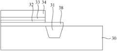
参照图3D并结合步骤S24,采用光刻及刻蚀工艺去除依次覆盖在所述浅沟槽隔离31上的所述第一覆盖层38、所述第二覆盖层38’、所述第二高K介质层32、所述第二金属栅材料层33’以及第二多晶硅层34’,以形成凹槽37。在本实施例中,第一覆盖层38的厚度为10nm~50nm,第二覆盖层38’的厚度为10nm~50nm,第一覆盖层38和第二覆盖层38’的材料均为氧化镧,第一覆盖层38以及第二覆盖层38’能够作为刻蚀阻挡层避免浅沟槽隔离31受到损伤,进一步避免了由于浅沟槽隔离31损伤引起的短路,提高了产品良率。本领域的普通技术人员应该理解,所述第一覆盖层38以及第二覆盖层38’的材料不仅仅局限于氧化镧,还可以是诸如氧化钬等材料。Referring to FIG. 3D and in conjunction with step S24, the
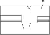
参照图3E、图3F并结合步骤S25,在第一多晶硅层34和第二多晶硅层34’上以及凹槽37内沉积多晶硅帽层35,利用光刻及刻蚀工艺在所述浅沟槽隔离31的两侧形成第一高K栅介质/金属栅结构36以及第二高K栅介质/金属栅结构36’。Referring to FIG. 3E, FIG. 3F and in conjunction with step S25, a
在本实施例中,所述第一金属栅材料层33的材料是氮化钛,所述第二金属栅材料层33’的材料是氮化钽,所述第一多晶硅层34和所述第二多晶硅层34’的材料均为多晶硅。In this embodiment, the material of the first metal
进一步地,所述第一高K介质层32与所述半导体衬底30之间形成有第一氧化硅层,所述第二高K介质层32’与所述半导体衬底30之间形成有第二氧化硅层,在本实施例中,并未在图中示出所述第一氧化硅层以及所述第二氧化硅层,但是所述第一氧化硅层和所述第二氧化硅层是存在的,本领域普通技术人员应该悉知。第一氧化硅层使得所述第一高K介质层32与所述半导体衬底30之间的粘附性更好,第二氧化硅层使得所述第二高K介质层32’与所述半导体衬底30之间的粘附性更好。而第一氧化硅层上的第一覆盖层38能够防止第一高K介质层32向第一氧化硅层扩散,第二氧化硅层上的第二覆盖层38’能够防止第二高K介质层32’向第二氧化硅层扩散。Further, a first silicon oxide layer is formed between the first high-
显然,本领域的技术人员可以对发明进行各种改动和变型而不脱离本发明的精神和范围。这样,倘若本发明的这些修改和变型属于本发明权利要求及其等同技术的范围之内,则本发明也意图包含这些改动和变型在内。Obviously, those skilled in the art can make various changes and modifications to the invention without departing from the spirit and scope of the invention. Thus, if these modifications and variations of the present invention fall within the scope of the claims of the present invention and their equivalent technologies, the present invention also intends to include these modifications and variations.
Claims (12)
Translated fromChinesePriority Applications (1)
| Application Number | Priority Date | Filing Date | Title |
|---|---|---|---|
| CN 201110335104CN102332398B (en) | 2011-10-28 | 2011-10-28 | Method for manufacturing two high-K gate dielectric/metal gate structures |
Applications Claiming Priority (1)
| Application Number | Priority Date | Filing Date | Title |
|---|---|---|---|
| CN 201110335104CN102332398B (en) | 2011-10-28 | 2011-10-28 | Method for manufacturing two high-K gate dielectric/metal gate structures |
Publications (2)
| Publication Number | Publication Date |
|---|---|
| CN102332398A CN102332398A (en) | 2012-01-25 |
| CN102332398Btrue CN102332398B (en) | 2012-12-12 |
Family
ID=45484125
Family Applications (1)
| Application Number | Title | Priority Date | Filing Date |
|---|---|---|---|
| CN 201110335104ActiveCN102332398B (en) | 2011-10-28 | 2011-10-28 | Method for manufacturing two high-K gate dielectric/metal gate structures |
Country Status (1)
| Country | Link |
|---|---|
| CN (1) | CN102332398B (en) |
Families Citing this family (1)
| Publication number | Priority date | Publication date | Assignee | Title |
|---|---|---|---|---|
| CN119173033A (en)* | 2024-08-02 | 2024-12-20 | 福建省晋华集成电路有限公司 | A method for preparing a semiconductor memory |
Citations (2)
| Publication number | Priority date | Publication date | Assignee | Title |
|---|---|---|---|---|
| CN101051638A (en)* | 2006-04-03 | 2007-10-10 | 台湾积体电路制造股份有限公司 | semiconductor element |
| CN101783316A (en)* | 2009-01-16 | 2010-07-21 | 台湾积体电路制造股份有限公司 | Method of implantation |
Family Cites Families (5)
| Publication number | Priority date | Publication date | Assignee | Title |
|---|---|---|---|---|
| US6787421B2 (en)* | 2002-08-15 | 2004-09-07 | Freescale Semiconductor, Inc. | Method for forming a dual gate oxide device using a metal oxide and resulting device |
| US8021939B2 (en)* | 2007-12-12 | 2011-09-20 | International Business Machines Corporation | High-k dielectric and metal gate stack with minimal overlap with isolation region and related methods |
| JP2010073985A (en)* | 2008-09-19 | 2010-04-02 | Toshiba Corp | Semiconductor device |
| JP5336814B2 (en)* | 2008-10-27 | 2013-11-06 | ルネサスエレクトロニクス株式会社 | Semiconductor device and manufacturing method thereof |
| US8309419B2 (en)* | 2009-02-04 | 2012-11-13 | Freescale Semiconductor, Inc. | CMOS integration with metal gate and doped high-K oxides |
- 2011
- 2011-10-28CNCN 201110335104patent/CN102332398B/enactiveActive
Patent Citations (2)
| Publication number | Priority date | Publication date | Assignee | Title |
|---|---|---|---|---|
| CN101051638A (en)* | 2006-04-03 | 2007-10-10 | 台湾积体电路制造股份有限公司 | semiconductor element |
| CN101783316A (en)* | 2009-01-16 | 2010-07-21 | 台湾积体电路制造股份有限公司 | Method of implantation |
Non-Patent Citations (3)
| Title |
|---|
| Guohua Wang等.Process challenges in CMOS FEOL for 32nm node.《Proceedings of 2008 9th International Conference on Solid-State and Integrated-Circuit Technology 》.2008,第1135-1138页. |
| JP特开2005-536053A 2005.11.24 |
| Process challenges in CMOS FEOL for 32nm node;Guohua Wang等;《Proceedings of 2008 9th International Conference on Solid-State and Integrated-Circuit Technology 》;20081231;第1135-1138页* |
Also Published As
| Publication number | Publication date |
|---|---|
| CN102332398A (en) | 2012-01-25 |
Similar Documents
| Publication | Publication Date | Title |
|---|---|---|
| TWI523237B (en) | Fin field effect transistor with source-drain sidewall spacers and reduced height | |
| CN109904120B (en) | Semiconductor device and method of manufacturing the same | |
| CN104037226B (en) | FinFET and its manufacture method with asymmetric source/drain structure | |
| TW201331996A (en) | Method of patterning features in a structure using multiple sidewall image transfer techniques | |
| US9384988B2 (en) | Gate protection caps and method of forming the same | |
| US10211108B2 (en) | Gate structures and fabrication methods thereof | |
| CN103531538B (en) | The formation method of CMOS (Complementary Metal Oxide Semiconductor) pipe | |
| JP2017504205A5 (en) | ||
| CN104681488B (en) | Transistor and forming method thereof | |
| US9627475B2 (en) | Dummy gate structure for semiconductor devices | |
| CN103474391A (en) | Method for forming high-k metal-gate device contact hole | |
| US9384996B2 (en) | Method for manufacturing semiconductor device and device manufactured by the same | |
| CN114420639A (en) | Semiconductor structure and manufacturing method thereof | |
| US20170294535A1 (en) | Semiconductor device and fabrication method thereof | |
| CN103854984B (en) | Manufacturing method of back gate process dummy gate and back gate process dummy gate | |
| CN106960875A (en) | Semiconductor device and its manufacture method | |
| CN105047613A (en) | Metal gate forming method | |
| CN102332398B (en) | Method for manufacturing two high-K gate dielectric/metal gate structures | |
| CN103531476B (en) | Semiconductor device manufacturing method | |
| TWI518789B (en) | Metal oxide semiconductor transistor and method of manufacturing the same | |
| CN105590861A (en) | Manufacturing method of transistor | |
| CN112563131B (en) | A method for preparing a metal gate device | |
| CN105633004A (en) | Self-Aligned Contact Fabrication Method | |
| CN104217951B (en) | A kind of semiconductor devices and its manufacture method | |
| CN103794479B (en) | A kind of manufacture method of semiconductor device |
Legal Events
| Date | Code | Title | Description |
|---|---|---|---|
| C06 | Publication | ||
| PB01 | Publication | ||
| C10 | Entry into substantive examination | ||
| SE01 | Entry into force of request for substantive examination | ||
| C14 | Grant of patent or utility model | ||
| GR01 | Patent grant | ||
| TR01 | Transfer of patent right | ||
| TR01 | Transfer of patent right | Effective date of registration:20250421 Address after:No.6 liangteng Road, Pudong New Area, Shanghai, 201314 Patentee after:SHANGHAI HUALI INTEGRATED CIRCUIT MANUFACTURING Co.,Ltd. Country or region after:China Address before:No. 497, Gaosi Road, Zhangjiang High Tech Park, Pudong New Area, Shanghai, 201203 Patentee before:Shanghai Huali Microelectronics Co.,Ltd. Country or region before:China |