CN102315354B - Packaging structure of light emitting diode - Google Patents
Packaging structure of light emitting diodeDownload PDFInfo
- Publication number
- CN102315354B CN102315354BCN2010102120688ACN201010212068ACN102315354BCN 102315354 BCN102315354 BCN 102315354BCN 2010102120688 ACN2010102120688 ACN 2010102120688ACN 201010212068 ACN201010212068 ACN 201010212068ACN 102315354 BCN102315354 BCN 102315354B
- Authority
- CN
- China
- Prior art keywords
- led
- package structure
- crystal grain
- transparency carrier
- transparent substrate
- Prior art date
- Legal status (The legal status is an assumption and is not a legal conclusion. Google has not performed a legal analysis and makes no representation as to the accuracy of the status listed.)
- Expired - Fee Related
Links
- 238000004806packaging method and processMethods0.000titleclaimsabstractdescription26
- 239000000758substrateSubstances0.000claimsabstractdescription60
- 229910052751metalInorganic materials0.000claimsabstractdescription51
- 239000002184metalSubstances0.000claimsabstractdescription51
- 239000013078crystalSubstances0.000claimsabstractdescription24
- 238000001816coolingMethods0.000claimsdescription15
- 239000011810insulating materialSubstances0.000claimsdescription6
- 239000000463materialSubstances0.000claimsdescription6
- VYPSYNLAJGMNEJ-UHFFFAOYSA-Nsilicon dioxideInorganic materialsO=[Si]=OVYPSYNLAJGMNEJ-UHFFFAOYSA-N0.000claimsdescription4
- 229910052581Si3N4Inorganic materials0.000claimsdescription2
- 239000011521glassSubstances0.000claimsdescription2
- 239000010453quartzSubstances0.000claimsdescription2
- HQVNEWCFYHHQES-UHFFFAOYSA-Nsilicon nitrideChemical compoundN12[Si]34N5[Si]62N3[Si]51N64HQVNEWCFYHHQES-UHFFFAOYSA-N0.000claimsdescription2
- 238000010438heat treatmentMethods0.000claims4
- 239000002390adhesive tapeSubstances0.000claims1
- 239000012774insulation materialSubstances0.000abstractdescription2
- 238000002834transmittanceMethods0.000abstractdescription2
- 239000004065semiconductorSubstances0.000description14
- 150000001875compoundsChemical class0.000description3
- 239000008393encapsulating agentSubstances0.000description3
- 239000003292glueSubstances0.000description3
- BPQQTUXANYXVAA-UHFFFAOYSA-NOrthosilicateChemical compound[O-][Si]([O-])([O-])[O-]BPQQTUXANYXVAA-UHFFFAOYSA-N0.000description2
- 230000005679Peltier effectEffects0.000description2
- OAICVXFJPJFONN-UHFFFAOYSA-NPhosphorusChemical compound[P]OAICVXFJPJFONN-UHFFFAOYSA-N0.000description2
- 239000000853adhesiveSubstances0.000description2
- 230000001070adhesive effectEffects0.000description2
- 230000000694effectsEffects0.000description2
- 238000005538encapsulationMethods0.000description2
- 239000003822epoxy resinSubstances0.000description2
- 238000000605extractionMethods0.000description2
- 239000007769metal materialSubstances0.000description2
- 229920000647polyepoxidePolymers0.000description2
- 239000000741silica gelSubstances0.000description2
- 229910002027silica gelInorganic materials0.000description2
- 229910002909Bi-TeInorganic materials0.000description1
- RYGMFSIKBFXOCR-UHFFFAOYSA-NCopperChemical compound[Cu]RYGMFSIKBFXOCR-UHFFFAOYSA-N0.000description1
- 229910019819Cr—SiInorganic materials0.000description1
- 229910017082Fe-SiInorganic materials0.000description1
- 229910017133Fe—SiInorganic materials0.000description1
- 229910018643Mn—SiInorganic materials0.000description1
- 229910019142PO4Inorganic materials0.000description1
- BQCADISMDOOEFD-UHFFFAOYSA-NSilverChemical compound[Ag]BQCADISMDOOEFD-UHFFFAOYSA-N0.000description1
- 229910008310Si—GeInorganic materials0.000description1
- UCKMPCXJQFINFW-UHFFFAOYSA-NSulphideChemical compound[S-2]UCKMPCXJQFINFW-UHFFFAOYSA-N0.000description1
- CSDREXVUYHZDNP-UHFFFAOYSA-NalumanylidynesiliconChemical compound[Al].[Si]CSDREXVUYHZDNP-UHFFFAOYSA-N0.000description1
- 229910052782aluminiumInorganic materials0.000description1
- XAGFODPZIPBFFR-UHFFFAOYSA-NaluminiumChemical compound[Al]XAGFODPZIPBFFR-UHFFFAOYSA-N0.000description1
- 230000005540biological transmissionEffects0.000description1
- 239000003086colorantSubstances0.000description1
- 229910052802copperInorganic materials0.000description1
- 239000010949copperSubstances0.000description1
- 238000005485electric heatingMethods0.000description1
- 239000002223garnetSubstances0.000description1
- 230000017525heat dissipationEffects0.000description1
- 238000009413insulationMethods0.000description1
- 238000000034methodMethods0.000description1
- 150000004767nitridesChemical class0.000description1
- 230000003287optical effectEffects0.000description1
- 238000001579optical reflectometryMethods0.000description1
- -1oxynitrideChemical compound0.000description1
- 239000002245particleSubstances0.000description1
- NBIIXXVUZAFLBC-UHFFFAOYSA-KphosphateChemical compound[O-]P([O-])([O-])=ONBIIXXVUZAFLBC-UHFFFAOYSA-K0.000description1
- 239000010452phosphateSubstances0.000description1
- 229920000642polymerPolymers0.000description1
- 239000000843powderSubstances0.000description1
- 238000002310reflectometryMethods0.000description1
- 239000002210silicon-based materialSubstances0.000description1
- 229910052709silverInorganic materials0.000description1
- 239000004332silverSubstances0.000description1
Images


Classifications
- H—ELECTRICITY
- H10—SEMICONDUCTOR DEVICES; ELECTRIC SOLID-STATE DEVICES NOT OTHERWISE PROVIDED FOR
- H10H—INORGANIC LIGHT-EMITTING SEMICONDUCTOR DEVICES HAVING POTENTIAL BARRIERS
- H10H20/00—Individual inorganic light-emitting semiconductor devices having potential barriers, e.g. light-emitting diodes [LED]
- H10H20/80—Constructional details
- H10H20/85—Packages
- H10H20/8506—Containers
- H—ELECTRICITY
- H01—ELECTRIC ELEMENTS
- H01L—SEMICONDUCTOR DEVICES NOT COVERED BY CLASS H10
- H01L25/00—Assemblies consisting of a plurality of semiconductor or other solid state devices
- H01L25/16—Assemblies consisting of a plurality of semiconductor or other solid state devices the devices being of types provided for in two or more different subclasses of H10B, H10D, H10F, H10H, H10K or H10N, e.g. forming hybrid circuits
- H01L25/167—Assemblies consisting of a plurality of semiconductor or other solid state devices the devices being of types provided for in two or more different subclasses of H10B, H10D, H10F, H10H, H10K or H10N, e.g. forming hybrid circuits comprising optoelectronic devices, e.g. LED, photodiodes
- H—ELECTRICITY
- H10—SEMICONDUCTOR DEVICES; ELECTRIC SOLID-STATE DEVICES NOT OTHERWISE PROVIDED FOR
- H10H—INORGANIC LIGHT-EMITTING SEMICONDUCTOR DEVICES HAVING POTENTIAL BARRIERS
- H10H20/00—Individual inorganic light-emitting semiconductor devices having potential barriers, e.g. light-emitting diodes [LED]
- H10H20/80—Constructional details
- H10H20/85—Packages
- H10H20/858—Means for heat extraction or cooling
- H10H20/8585—Means for heat extraction or cooling being an interconnection
- H—ELECTRICITY
- H01—ELECTRIC ELEMENTS
- H01L—SEMICONDUCTOR DEVICES NOT COVERED BY CLASS H10
- H01L2224/00—Indexing scheme for arrangements for connecting or disconnecting semiconductor or solid-state bodies and methods related thereto as covered by H01L24/00
- H01L2224/01—Means for bonding being attached to, or being formed on, the surface to be connected, e.g. chip-to-package, die-attach, "first-level" interconnects; Manufacturing methods related thereto
- H01L2224/42—Wire connectors; Manufacturing methods related thereto
- H01L2224/47—Structure, shape, material or disposition of the wire connectors after the connecting process
- H01L2224/48—Structure, shape, material or disposition of the wire connectors after the connecting process of an individual wire connector
- H01L2224/4805—Shape
- H01L2224/4809—Loop shape
- H01L2224/48091—Arched
- H—ELECTRICITY
- H10—SEMICONDUCTOR DEVICES; ELECTRIC SOLID-STATE DEVICES NOT OTHERWISE PROVIDED FOR
- H10H—INORGANIC LIGHT-EMITTING SEMICONDUCTOR DEVICES HAVING POTENTIAL BARRIERS
- H10H20/00—Individual inorganic light-emitting semiconductor devices having potential barriers, e.g. light-emitting diodes [LED]
- H10H20/80—Constructional details
- H10H20/85—Packages
- H10H20/855—Optical field-shaping means, e.g. lenses
- H10H20/856—Reflecting means
- H—ELECTRICITY
- H10—SEMICONDUCTOR DEVICES; ELECTRIC SOLID-STATE DEVICES NOT OTHERWISE PROVIDED FOR
- H10H—INORGANIC LIGHT-EMITTING SEMICONDUCTOR DEVICES HAVING POTENTIAL BARRIERS
- H10H20/00—Individual inorganic light-emitting semiconductor devices having potential barriers, e.g. light-emitting diodes [LED]
- H10H20/80—Constructional details
- H10H20/85—Packages
- H10H20/857—Interconnections, e.g. lead-frames, bond wires or solder balls
- H—ELECTRICITY
- H10—SEMICONDUCTOR DEVICES; ELECTRIC SOLID-STATE DEVICES NOT OTHERWISE PROVIDED FOR
- H10H—INORGANIC LIGHT-EMITTING SEMICONDUCTOR DEVICES HAVING POTENTIAL BARRIERS
- H10H20/00—Individual inorganic light-emitting semiconductor devices having potential barriers, e.g. light-emitting diodes [LED]
- H10H20/80—Constructional details
- H10H20/882—Scattering means
Landscapes
- Engineering & Computer Science (AREA)
- Microelectronics & Electronic Packaging (AREA)
- Physics & Mathematics (AREA)
- Condensed Matter Physics & Semiconductors (AREA)
- General Physics & Mathematics (AREA)
- Computer Hardware Design (AREA)
- Power Engineering (AREA)
- Led Device Packages (AREA)
Abstract
Description
Translated fromChinese技术领域technical field
本发明涉及一种发光二极管,特别是指一种发光二极管的封装结构。The invention relates to a light emitting diode, in particular to a packaging structure of a light emitting diode.
背景技术Background technique
发光二极管(Light Emitting Diode,LED)为一种半导体光源,其电、光特性及寿命对温度敏感,在此,一种在温度变化过程中还能保持稳定光强的新型发光二极管可参见Yukio Tanaka等人在文献IEEE Transactions On ElectronDevices,Vol.41,No.7,July 1994中的A Novel Temperature-StableLight-Emitting Diode一文。A light emitting diode (Light Emitting Diode, LED) is a semiconductor light source, and its electrical, optical characteristics and life are sensitive to temperature. Here, a new type of light emitting diode that can maintain a stable light intensity during temperature changes can be found in Yukio Tanaka et al. A Novel Temperature-StableLight-Emitting Diode in the document IEEE Transactions On ElectronDevices, Vol.41, No.7, July 1994.
目前,提高LED的亮度是研究LED的一大课题。作为提高亮度的手段,考虑或提高LED内部的量子的效率,或提高LED芯片在封装结构中发出的光的出光效率。如图1所示,一种现有的发光二极管的封装结构10包括:一基板11、一反射杯18围绕于该基板11周围、一对电极12及13设置在基板11上、一晶粒15贴设在该电极12上且分别通过导线17连接该对电极12及13、一封装胶16填充于该反射杯18内并覆盖该晶粒15。该晶粒15发出的光线经过反光杯18内表面反射从顶部射出。然而,由于反光杯18的出光口限制了出光面,使得封装结构10的出光面积S较小,若为了增加出光面积,必须增加基板的面积,导致整个封装结构的体积变大,并不符合现在工业上的需求。At present, improving the brightness of LED is a major topic of LED research. As a means to improve brightness, it is considered to improve the quantum efficiency inside the LED, or to improve the light extraction efficiency of the light emitted by the LED chip in the packaging structure. As shown in FIG. 1 , a conventional
发明内容Contents of the invention
有鉴于此,有提供一种出光面积大、出光效率高的发光二极管的封装结构。In view of this, there is provided a packaging structure of a light emitting diode with a large light emitting area and high light emitting efficiency.
一种发光二极管封装结构,包括一透明基板、一设置于透明基板上的凹槽、及一位于该凹槽底部的晶粒,透明基板具有一第一表面、一第二表面以及连接所述第一表面及第二表面的侧面,该凹槽位于该透明基板的第一表面,该发光二极管封装结构还包括覆盖于所述透明基板的第二表面及侧面的一金属层,一对金属电极位于凹槽底部并延伸穿过所述透明基板的第二表面及金属层,一绝缘材料隔绝该金属电极与该金属层;金属层将晶粒发出的并穿过透明基板的光线反射出去。A light-emitting diode packaging structure, comprising a transparent substrate, a groove arranged on the transparent substrate, and a crystal grain located at the bottom of the groove, the transparent substrate has a first surface, a second surface and connecting the first surface The first surface and the side of the second surface, the groove is located on the first surface of the transparent substrate, the light emitting diode packaging structure also includes a metal layer covering the second surface and the side of the transparent substrate, a pair of metal electrodes are located The bottom of the groove extends through the second surface of the transparent substrate and the metal layer, and an insulating material isolates the metal electrode and the metal layer; the metal layer reflects the light emitted by the crystal grain and passes through the transparent substrate.
相对于现有技术,本发明透明基板的光透性更提高发光二极管封装结构的出光面积及出光效率。Compared with the prior art, the light transmittance of the transparent substrate of the present invention further improves the light output area and light output efficiency of the LED packaging structure.
下面参照附图,结合具体实施例对本发明作进一步的描述。The present invention will be further described below in conjunction with specific embodiments with reference to the accompanying drawings.
附图说明Description of drawings
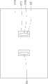
图1为现有技术的发光二极管的封装结构的剖面示意图。FIG. 1 is a schematic cross-sectional view of a packaging structure of a light emitting diode in the prior art.
图2为本发明第一实施例的发光二极管的封装结构的剖面示意图。FIG. 2 is a schematic cross-sectional view of the package structure of the light emitting diode according to the first embodiment of the present invention.
图3为图2的发光二极管的封装结构的俯视图。FIG. 3 is a top view of the package structure of the light emitting diode shown in FIG. 2 .
图4为图2的发光二极管的封装结构的仰视图。FIG. 4 is a bottom view of the packaging structure of the light emitting diode in FIG. 2 .
图5为本发明第二实施例的发光二极管的封装结构的剖面示意图。5 is a schematic cross-sectional view of a package structure of a light emitting diode according to a second embodiment of the present invention.
主要元件符号说明Description of main component symbols
具体实施方式Detailed ways
请参阅图2至图3,本发明第一实施例发光二极管的封装结构20包括一透明基板29、一晶粒24、及二金属电极25。该透明基板29具有一第一表面291、一与第一表面291相对的第二表面292及连接第一、第二表面291、292的侧面293。该透明基板29在第一表面291上设有一凹槽296。所述晶粒24通过一导热基板23设置在凹槽296的底部。该发光二极管的封装结构20还包括一金属层27覆盖于所述透明基板29的第二表面292及侧面293。所述二电极25位于凹槽296底部并延伸至所述透明基板29的第二表面292及穿过金属层27,并利用一绝缘材料295与所述金属层27隔绝。一导热系统设置在透明基板29内连接导热基板23与金属层27,以将该晶粒24产生的热量由导热系统传递至金属层27。本实施例中的导热系统为一导热柱28。该导热柱28设置于所述导热基板23下方并延伸至所述透明基板29的第二表面292连接所述金属层27。Please refer to FIG. 2 to FIG. 3 , the
该晶粒24可以为III-V族化合物半导体芯片或II-VI族化合物半导体芯片,并且该晶粒24发出的光包含可见光或不可见光或可见光与不可见光之混光,例如:紫外(UV)光、蓝光、绿光或多种波长光之混光。The
所述二电极25分别置于凹槽296两侧,且每一电极25的顶端并分别通过导线253与晶粒24连接。每一电极25的底端均穿置于所述透明基板29及所述金属层27。一绝缘材料隔绝所述金属层27及所述二电极25以防止结构短路的问题,所述绝缘材料可使用硅胶、环氧树脂等。The two
该透明基板29可选用石英、氮化硅、玻璃或透明胶材等可透光性材质。一封装胶26填充于所述凹槽296内以保护晶粒24。该封装胶26可选用硅胶、环氧树脂等透明胶材。封装胶26内可添加合适的荧光粉265,以增加不同的出光颜色。所述荧光粉265可以为石榴石(garnet)结构的化合物、硫化物(sulfide)、磷化物(phosphate)、氮化物(nitride)、氮氧化物(oxynitride)、硅铝氧氮聚合物(SiAlON)或硅酸盐类(silicate)。The
请一并参阅图4,所述金属层27覆盖于所述透明基板29的第二表面292及侧面293,将整个发光二极管的封装结构20的侧部及底部围设。该金属层27由具有发射功能及导热性能良好的金属材料支撑,可依据晶粒发出的波长选择适当的金属材料,如铜、铝或银等等。该金属层27包括一覆盖于透明基板29的第二表面292的底板275及覆盖于透明基板29的侧面293的侧壁276。金属层27的底板275设有二间隔的穿孔271,该穿孔的形状不限,主要依据电极25形状而定,以供电极25的底端穿设。其中每一穿孔271的尺寸均大于对应的电极25的尺寸,并且使金属层27的底板275与每一电极25的底端均匀间隔以填充所述绝缘材料295,以防止电极25与金属层27电连接而发生漏电。该侧壁276与底板275呈一θ角倾斜设置,以将晶粒24发出的光线透过封装胶26后反射出。在本实施例中,该θ角的值可以是大于90度且小于150度中选择一个合适值以改变侧壁276的倾斜角以提高光的反射率,此时,发光二极管的封装结构20的出光面积A相对现有技术的出光面积S较大。Please also refer to FIG. 4 , the
该导热柱28连接金属层27的底板275与导热基板23,以将晶粒24产生的热量迅速传递至金属层27上。可以理解地,该发光二极管的封装结构20的晶粒24数量可以是多个,每一晶粒24可对应设置一导热柱28连接所述金属层27,或者设置一单个的导热柱28一端同时连接所有晶粒24,另一端连接金属层27。The
本发明之发光二极管封装结构工作时,由于透明基板29的透光作用,使晶粒24发出的光线穿过透明基板29的侧面293且经由金属层27的侧壁276朝出光面反射出去,增大了发光二极管的封装结构20的出光面积A及出光率。同时,金属层27的侧壁276与底板275之间的θ角亦可以根据设计需要选择一个合适值以提高光的反射率。另外,晶粒24产生的热量直接通过导热柱28迅速传递至金属层27的底板275及侧壁276,使得发光二极管的封装结构20具有良好的散热性能,有别于传统封装结构只利用导线传导电热更能够增加发光二极管的使用寿命。When the light-emitting diode package structure of the present invention works, due to the light-transmitting effect of the
请参阅图5,为本发明第二实施例的发光二极管的封装结构30,包括一透明基板39、一晶粒34、二电极35、一覆盖于所述透明基板39的金属层37、及一导热系统。与第一实施例中的发光二极管的封装结构20的不同之处在于,该发光二极管的封装结构30的透明基板39的第一表面391为粗糙面,即其上设置凹凸的刻纹,以降低光线在透明基板39内出现全反射的概率,增加发光二极管的封装结构30的出光率。Please refer to FIG. 5, which is a
另外,与第一实施例中的发光二极管的封装结构20的不同之处还在于,本实施例中的导热系统为一热电致冷器,该热电致冷器(图未标)包括一与晶粒34接触的第一基板381、与金属层37接触的第二基板382、置于第一基板381与第二基板382之间的热电致冷单元组。In addition, the difference from the
该第一基板381及第二基板382均可为绝缘性及导热性较好的材料制成。该热电致冷单元组包括若干串联在一起的热电致冷单元384。在本实施例中,相邻两个热电致冷单元384通过一导电片385形成电连接。每个热电致冷单元384包括一导电基底386、及设置在该导电基底386一侧并分别与该导电基底386电连接的P型半导体块387与N型半导体块388。该热电致冷单元组的两端分别与一直流电源40相连,其中图5中直流电源40与发光二极管的封装结构30的位置关系仅为简单示意,并非具体的实物连接。Both the
该P型半导体块387与该N型半导体块388分别为掺杂有Bi-Te系、Sb-Te系、Bi-Se系、Pb-Te系、Ag-Sb-Te系、Si-Ge系、Fe-Si系、Mn-Si系或者Cr-Si系化合物半导体的固态块体(Solid-State Cube)。在本实施例中,该P型半导体块387与该N型半导体块388分别为P型Bi2Te3、N型Bi2Te3。The P-
当直流电源40给热电致冷单元组提供电能时,热电致冷单元组所包括的多个热电致冷单元384均会产生帕贴尔效应(Peltier Effect),该热电致冷单元组的靠近第一基板381一端的热量可以通过P型半导体块387及N型半导体块388的传输作用被传送到靠近第二基板382一端。在此,该晶粒24发出的热量经由导热性佳的第一基板381传导至该多个热电致冷单元384,再通过P型半导体块387及N型半导体块388的传输作用将热量传送到该第二基板382,接着经由金属层37快速传导出去。When the
另外,本领域技术人员还可以在本发明精神内做其它变化,例如适当变更透明基板、金属层的材质及形状、凹槽的深度,以及将热管、平板热管作为导热系统等,当然,这些依据本发明精神所做的变化,都应包含在本发明所要求保护的范围之内。In addition, those skilled in the art can also make other changes within the spirit of the present invention, such as appropriately changing the material and shape of the transparent substrate, the metal layer, the depth of the groove, and using heat pipes and flat heat pipes as heat conduction systems, etc. Of course, these basis All changes made in the spirit of the present invention should be included within the scope of protection claimed by the present invention.
Claims (10)
Priority Applications (2)
| Application Number | Priority Date | Filing Date | Title |
|---|---|---|---|
| CN2010102120688ACN102315354B (en) | 2010-06-29 | 2010-06-29 | Packaging structure of light emitting diode |
| US12/986,187US8288789B2 (en) | 2010-06-29 | 2011-01-07 | LED package |
Applications Claiming Priority (1)
| Application Number | Priority Date | Filing Date | Title |
|---|---|---|---|
| CN2010102120688ACN102315354B (en) | 2010-06-29 | 2010-06-29 | Packaging structure of light emitting diode |
Publications (2)
| Publication Number | Publication Date |
|---|---|
| CN102315354A CN102315354A (en) | 2012-01-11 |
| CN102315354Btrue CN102315354B (en) | 2013-11-06 |
Family
ID=45351693
Family Applications (1)
| Application Number | Title | Priority Date | Filing Date |
|---|---|---|---|
| CN2010102120688AExpired - Fee RelatedCN102315354B (en) | 2010-06-29 | 2010-06-29 | Packaging structure of light emitting diode |
Country Status (2)
| Country | Link |
|---|---|
| US (1) | US8288789B2 (en) |
| CN (1) | CN102315354B (en) |
Families Citing this family (33)
| Publication number | Priority date | Publication date | Assignee | Title |
|---|---|---|---|---|
| US9780268B2 (en) | 2006-04-04 | 2017-10-03 | Cree, Inc. | Submount based surface mount device (SMD) light emitter components and methods |
| KR101055095B1 (en)* | 2010-03-09 | 2011-08-08 | 엘지이노텍 주식회사 | Light emitting device |
| US8436386B2 (en)* | 2011-06-03 | 2013-05-07 | Micron Technology, Inc. | Solid state lighting devices having side reflectivity and associated methods of manufacture |
| US9460972B2 (en)* | 2012-01-09 | 2016-10-04 | STATS ChipPAC Pte. Ltd. | Semiconductor device and method of forming reduced surface roughness in molded underfill for improved C-SAM inspection |
| CN103220884A (en)* | 2012-01-18 | 2013-07-24 | 光宏精密股份有限公司 | Circuit substrate structure and manufacturing method thereof |
| TW201336114A (en)* | 2012-02-22 | 2013-09-01 | 矽品精密工業股份有限公司 | Semiconductor package and method of forming same |
| US9735198B2 (en) | 2012-03-30 | 2017-08-15 | Cree, Inc. | Substrate based light emitter devices, components, and related methods |
| US10222032B2 (en) | 2012-03-30 | 2019-03-05 | Cree, Inc. | Light emitter components and methods having improved electrical contacts |
| US10134961B2 (en) | 2012-03-30 | 2018-11-20 | Cree, Inc. | Submount based surface mount device (SMD) light emitter components and methods |
| CN103456726B (en)* | 2012-05-31 | 2020-06-26 | 惠州科锐半导体照明有限公司 | LED package, LED display, and method of manufacturing LED package |
| AU2012244393B1 (en)* | 2012-11-07 | 2013-10-10 | Chao-Chin Yeh | LED Cooling Structure |
| CN103022319A (en)* | 2012-12-17 | 2013-04-03 | 四川鼎吉光电科技有限公司 | Light emitting diode (LED) encapsulating structure |
| US10439111B2 (en) | 2014-05-14 | 2019-10-08 | Genesis Photonics Inc. | Light emitting device and manufacturing method thereof |
| US9997676B2 (en) | 2014-05-14 | 2018-06-12 | Genesis Photonics Inc. | Light emitting device and manufacturing method thereof |
| TWI578574B (en)* | 2014-07-14 | 2017-04-11 | 新世紀光電股份有限公司 | Light-emitting element structure |
| US12364074B2 (en) | 2015-03-31 | 2025-07-15 | Creeled, Inc. | Light emitting diodes and methods |
| CN113130725B (en) | 2015-03-31 | 2024-09-24 | 科锐Led公司 | Light emitting diode with encapsulation and method |
| CN106549092A (en) | 2015-09-18 | 2017-03-29 | 新世纪光电股份有限公司 | Light emitting device and method for manufacturing the same |
| US20170141278A1 (en)* | 2015-11-17 | 2017-05-18 | Toshiba Corporation | Led assembly for led package with sidewall electrodes |
| US10824054B2 (en) | 2017-01-24 | 2020-11-03 | Lg Electronics Inc. | Mobile terminal |
| WO2018139790A1 (en)* | 2017-01-24 | 2018-08-02 | 엘지전자 주식회사 | Mobile/portable terminal |
| DE112018000874B4 (en)* | 2017-02-15 | 2024-09-12 | Ferrotec Material Technologies Corporation | HOUSING WITH BUILT-IN THERMOELECTRIC ELEMENT |
| US10672957B2 (en) | 2017-07-19 | 2020-06-02 | Cree, Inc. | LED apparatuses and methods for high lumen output density |
| CN109994458B (en) | 2017-11-05 | 2022-07-01 | 新世纪光电股份有限公司 | light-emitting device |
| TW202249306A (en) | 2017-11-05 | 2022-12-16 | 新世紀光電股份有限公司 | Light emitting apparatus |
| CN110197619B (en)* | 2018-02-27 | 2021-04-23 | 欣兴电子股份有限公司 | Pixel structure and method of making pixel structure |
| CN110391321B (en)* | 2018-04-19 | 2021-05-28 | 展晶科技(深圳)有限公司 | Light emitting diode package and method of making the same |
| CN108598246A (en)* | 2018-07-13 | 2018-09-28 | 广东格斯泰气密元件有限公司 | A kind of SMD-UV-LED of vacuum tight encapsulation |
| US10622272B1 (en)* | 2018-10-24 | 2020-04-14 | Advanced Semiconductor Engineering, Inc. | Semiconductor chip structure and semiconductor package |
| CN111463335B (en)* | 2020-05-11 | 2024-09-03 | 福建省信达光电科技有限公司 | LED bracket, LED lamp bead and LED lamp |
| US11789221B2 (en)* | 2021-10-05 | 2023-10-17 | Aeva, Inc. | Techniques for device cooling in an optical sub-assembly |
| CN114914345A (en)* | 2022-03-25 | 2022-08-16 | 硅能光电半导体(广州)有限公司 | Packaging method of LED lamp beads |
| CN117276213B (en)* | 2023-09-28 | 2025-07-04 | 东莞市冠晶电子有限公司 | A fast recovery diode frame structure with high heat dissipation |
Citations (4)
| Publication number | Priority date | Publication date | Assignee | Title |
|---|---|---|---|---|
| CN1396667A (en)* | 2001-07-16 | 2003-02-12 | 诠兴开发科技股份有限公司 | LED packaging |
| WO2008099784A1 (en)* | 2007-02-15 | 2008-08-21 | Panasonic Electric Works Co., Ltd. | Led package and structure for mounting three-dimensional circuit component |
| CN101449392A (en)* | 2006-05-31 | 2009-06-03 | 株式会社藤仓 | Substrate for mounting light-emitting element, light-emitting element package, display device, and lighting device |
| CN101578712A (en)* | 2006-11-14 | 2009-11-11 | 哈利盛东芝照明株式会社 | Light emitting device, its manufacturing method and its mounted substrate |
Family Cites Families (14)
| Publication number | Priority date | Publication date | Assignee | Title |
|---|---|---|---|---|
| US4966862A (en)* | 1989-08-28 | 1990-10-30 | Cree Research, Inc. | Method of production of light emitting diodes |
| JP4024994B2 (en)* | 2000-06-30 | 2007-12-19 | 株式会社東芝 | Semiconductor light emitting device |
| MY145695A (en)* | 2001-01-24 | 2012-03-30 | Nichia Corp | Light emitting diode, optical semiconductor device, epoxy resin composition suited for optical semiconductor device, and method for manufacturing the same |
| JP3707688B2 (en)* | 2002-05-31 | 2005-10-19 | スタンレー電気株式会社 | Light emitting device and manufacturing method thereof |
| US7095053B2 (en)* | 2003-05-05 | 2006-08-22 | Lamina Ceramics, Inc. | Light emitting diodes packaged for high temperature operation |
| US7274044B2 (en)* | 2004-01-26 | 2007-09-25 | Semiconductor Energy Laboratory Co., Ltd. | Light emitting device |
| KR101241650B1 (en)* | 2005-10-19 | 2013-03-08 | 엘지이노텍 주식회사 | Package of light emitting diode |
| KR101171186B1 (en)* | 2005-11-10 | 2012-08-06 | 삼성전자주식회사 | High luminance light emitting diode and liquid crystal display panel of using the same |
| JP2007157852A (en)* | 2005-12-01 | 2007-06-21 | Sony Corp | Semiconductor light emitting device and manufacturing method thereof |
| US7828460B2 (en)* | 2006-04-18 | 2010-11-09 | Cree, Inc. | Lighting device and lighting method |
| KR100845856B1 (en)* | 2006-12-21 | 2008-07-14 | 엘지전자 주식회사 | Light emitting device package and its manufacturing method |
| JP5154819B2 (en)* | 2007-04-03 | 2013-02-27 | 新光電気工業株式会社 | Substrate and manufacturing method thereof |
| KR101327106B1 (en)* | 2007-08-09 | 2013-11-07 | 엘지이노텍 주식회사 | Semiconductor light emitting device |
| DE102009018603B9 (en)* | 2008-04-25 | 2021-01-14 | Samsung Electronics Co., Ltd. | Lighting device and manufacturing method thereof |
- 2010
- 2010-06-29CNCN2010102120688Apatent/CN102315354B/ennot_activeExpired - Fee Related
- 2011
- 2011-01-07USUS12/986,187patent/US8288789B2/ennot_activeExpired - Fee Related
Patent Citations (4)
| Publication number | Priority date | Publication date | Assignee | Title |
|---|---|---|---|---|
| CN1396667A (en)* | 2001-07-16 | 2003-02-12 | 诠兴开发科技股份有限公司 | LED packaging |
| CN101449392A (en)* | 2006-05-31 | 2009-06-03 | 株式会社藤仓 | Substrate for mounting light-emitting element, light-emitting element package, display device, and lighting device |
| CN101578712A (en)* | 2006-11-14 | 2009-11-11 | 哈利盛东芝照明株式会社 | Light emitting device, its manufacturing method and its mounted substrate |
| WO2008099784A1 (en)* | 2007-02-15 | 2008-08-21 | Panasonic Electric Works Co., Ltd. | Led package and structure for mounting three-dimensional circuit component |
Also Published As
| Publication number | Publication date |
|---|---|
| CN102315354A (en) | 2012-01-11 |
| US8288789B2 (en) | 2012-10-16 |
| US20110316024A1 (en) | 2011-12-29 |
Similar Documents
| Publication | Publication Date | Title |
|---|---|---|
| CN102315354B (en) | Packaging structure of light emitting diode | |
| US11450791B2 (en) | LED assembly for omnidirectional light applications | |
| US9620682B2 (en) | Light emitting device | |
| US8067782B2 (en) | LED package and light source device using same | |
| CN101465345B (en) | Light source device Light source die set and method for manufacturing the light source device | |
| US9153622B2 (en) | Series of light emitting regions with an intermediate pad | |
| TWI613842B (en) | Illuminating device | |
| CN103715188B (en) | LED emitter with improved white appearance | |
| CN102270725A (en) | Light-emitting diode packaging structure | |
| TWI549319B (en) | Light-emitting diode light-emitting device, method for packaging light-emitting diode, and method for packaging crystal grains | |
| EP2827387B1 (en) | Light emitting device | |
| CN103187408A (en) | Light-emitting diode packaging structure | |
| CN102376845A (en) | Packaging structure of light-emitting diode | |
| CN101477981A (en) | Light source module and manufacturing process thereof | |
| CN104566292B (en) | A kind of specular removal high heat conduction radiator structure of the comprehensive light extractions of LED | |
| CN102054905A (en) | Light emitting diode chip with heat conducting layers | |
| CN108352423A (en) | Semiconductor devices | |
| US8907371B2 (en) | Light emitting diode package and light emitting device having the same | |
| TWI407599B (en) | Package structure of led | |
| CN104037300A (en) | Light-emitting diode device and display device and electronic equipment | |
| CN102332526B (en) | Flip-chip light-emitting diode (LED) packaging structure | |
| CN105845804B (en) | Light emitting diode device and light emitting device using same | |
| US20110233583A1 (en) | High-power led package | |
| CN104037298A (en) | Method and apparatus for encapsulating phosphor-coated LEDs | |
| CN102945912A (en) | LED (Light Emitting Diode) light-emitting component bracket |
Legal Events
| Date | Code | Title | Description |
|---|---|---|---|
| C06 | Publication | ||
| PB01 | Publication | ||
| C10 | Entry into substantive examination | ||
| SE01 | Entry into force of request for substantive examination | ||
| C14 | Grant of patent or utility model | ||
| GR01 | Patent grant | ||
| CF01 | Termination of patent right due to non-payment of annual fee | Granted publication date:20131106 Termination date:20150629 | |
| EXPY | Termination of patent right or utility model |