CN102290532A - Organic electroluminescent element with high light extraction rate and optimization method thereof - Google Patents
Organic electroluminescent element with high light extraction rate and optimization method thereofDownload PDFInfo
- Publication number
- CN102290532A CN102290532ACN2011102123375ACN201110212337ACN102290532ACN 102290532 ACN102290532 ACN 102290532ACN 2011102123375 ACN2011102123375 ACN 2011102123375ACN 201110212337 ACN201110212337 ACN 201110212337ACN 102290532 ACN102290532 ACN 102290532A
- Authority
- CN
- China
- Prior art keywords
- base material
- organic electroluminescent
- light extraction
- reflectivity
- electroluminescent device
- Prior art date
- Legal status (The legal status is an assumption and is not a legal conclusion. Google has not performed a legal analysis and makes no representation as to the accuracy of the status listed.)
- Pending
Links
- 238000000605extractionMethods0.000titleclaimsabstractdescription31
- 238000000034methodMethods0.000titleclaimsabstractdescription16
- 238000005457optimizationMethods0.000titledescription4
- 230000003287optical effectEffects0.000claimsabstractdescription43
- 239000000758substrateSubstances0.000claimsabstractdescription26
- 238000002834transmittanceMethods0.000claimsabstractdescription26
- 238000002310reflectometryMethods0.000claimsabstractdescription24
- 239000000463materialSubstances0.000claimsdescription55
- 239000002245particleSubstances0.000claimsdescription19
- VTYYLEPIZMXCLO-UHFFFAOYSA-LCalcium carbonateChemical compound[Ca+2].[O-]C([O-])=OVTYYLEPIZMXCLO-UHFFFAOYSA-L0.000claimsdescription12
- VYPSYNLAJGMNEJ-UHFFFAOYSA-NSilicium dioxideChemical compoundO=[Si]=OVYPSYNLAJGMNEJ-UHFFFAOYSA-N0.000claimsdescription12
- GWEVSGVZZGPLCZ-UHFFFAOYSA-NTitan oxideChemical compoundO=[Ti]=OGWEVSGVZZGPLCZ-UHFFFAOYSA-N0.000claimsdescription11
- XLOMVQKBTHCTTD-UHFFFAOYSA-NZinc monoxideChemical compound[Zn]=OXLOMVQKBTHCTTD-UHFFFAOYSA-N0.000claimsdescription11
- TZCXTZWJZNENPQ-UHFFFAOYSA-Lbarium sulfateChemical compound[Ba+2].[O-]S([O-])(=O)=OTZCXTZWJZNENPQ-UHFFFAOYSA-L0.000claimsdescription11
- PNEYBMLMFCGWSK-UHFFFAOYSA-NAluminaChemical compound[O-2].[O-2].[O-2].[Al+3].[Al+3]PNEYBMLMFCGWSK-UHFFFAOYSA-N0.000claimsdescription7
- MCMNRKCIXSYSNV-UHFFFAOYSA-NZrO2Inorganic materialsO=[Zr]=OMCMNRKCIXSYSNV-UHFFFAOYSA-N0.000claimsdescription6
- 229910000019calcium carbonateInorganic materials0.000claimsdescription6
- RVTZCBVAJQQJTK-UHFFFAOYSA-Noxygen(2-);zirconium(4+)Chemical compound[O-2].[O-2].[Zr+4]RVTZCBVAJQQJTK-UHFFFAOYSA-N0.000claimsdescription6
- 239000000377silicon dioxideSubstances0.000claimsdescription6
- 235000012239silicon dioxideNutrition0.000claimsdescription6
- -1yittrium oxideChemical compound0.000claimsdescription6
- 239000011248coating agentSubstances0.000claimsdescription5
- 238000000576coating methodMethods0.000claimsdescription5
- 239000004408titanium dioxideSubstances0.000claimsdescription5
- 239000011787zinc oxideSubstances0.000claimsdescription5
- 239000003595mistSubstances0.000claims7
- 229910052771TerbiumInorganic materials0.000claims2
- 239000002223garnetSubstances0.000claims2
- GZCRRIHWUXGPOV-UHFFFAOYSA-Nterbium atomChemical compound[Tb]GZCRRIHWUXGPOV-UHFFFAOYSA-N0.000claims2
- 239000002105nanoparticleSubstances0.000description18
- 238000005401electroluminescenceMethods0.000description5
- 229910019901yttrium aluminum garnetInorganic materials0.000description5
- 239000011521glassSubstances0.000description4
- SIWVEOZUMHYXCS-UHFFFAOYSA-Noxo(oxoyttriooxy)yttriumChemical compoundO=[Y]O[Y]=OSIWVEOZUMHYXCS-UHFFFAOYSA-N0.000description4
- 238000002347injectionMethods0.000description3
- 239000007924injectionSubstances0.000description3
- 229910052751metalInorganic materials0.000description3
- 239000002184metalSubstances0.000description3
- TWNQGVIAIRXVLR-UHFFFAOYSA-Noxo(oxoalumanyloxy)alumaneChemical compoundO=[Al]O[Al]=OTWNQGVIAIRXVLR-UHFFFAOYSA-N0.000description3
- 238000010586diagramMethods0.000description2
- 230000005281excited stateEffects0.000description2
- 230000031700light absorptionEffects0.000description2
- 229910018072Al 2 O 3Inorganic materials0.000description1
- 229910004298SiO 2Inorganic materials0.000description1
- JNDMLEXHDPKVFC-UHFFFAOYSA-Naluminum;oxygen(2-);yttrium(3+)Chemical compound[O-2].[O-2].[O-2].[Al+3].[Y+3]JNDMLEXHDPKVFC-UHFFFAOYSA-N0.000description1
- 230000015572biosynthetic processEffects0.000description1
- 239000002131composite materialSubstances0.000description1
- 230000000694effectsEffects0.000description1
- 230000005684electric fieldEffects0.000description1
- 230000005283ground stateEffects0.000description1
- 230000005525hole transportEffects0.000description1
- AMGQUBHHOARCQH-UHFFFAOYSA-Nindium;oxotinChemical compound[In].[Sn]=OAMGQUBHHOARCQH-UHFFFAOYSA-N0.000description1
- 239000011159matrix materialSubstances0.000description1
- 238000005259measurementMethods0.000description1
- 238000012986modificationMethods0.000description1
- 230000004048modificationEffects0.000description1
- 229920000642polymerPolymers0.000description1
- 239000002861polymer materialSubstances0.000description1
- 239000004065semiconductorSubstances0.000description1
- 229910052710siliconInorganic materials0.000description1
- 239000010703siliconSubstances0.000description1
- 229910019655synthetic inorganic crystalline materialInorganic materials0.000description1
Images

Landscapes
- Electroluminescent Light Sources (AREA)
Abstract
Description
Translated fromChinese技术领域technical field
本发明涉及一种有机电致发光元件,且尤其涉及一种具有高光取出率的有机电致发光元件及其光取出率的最适化方法。The present invention relates to an organic electroluminescence element, and in particular to an organic electroluminescence element with high light extraction rate and an optimization method for the light extraction rate.
背景技术Background technique
有机电致发光元件,例如有机发光二极管(organic light emitting diode;OLED)元件,具有高亮度、屏幕反应速度快、轻薄短小、全彩、无视角差、不需背光以及节省灯源及耗电量,因而已成为新一代显示器的主要光源。Organic electroluminescent components, such as organic light emitting diode (OLED) components, have high brightness, fast screen response, thin and short, full color, no viewing angle difference, no backlight, and save light source and power consumption , thus has become the main light source of the new generation of displays.
典型的有机电致发光元件,包含透明基板、透明的阳极、空穴注入层、具电子传输功能的发光层及金属阴极。当施以一顺向偏压电压时,空穴由阳极注入,而电子由阴极注入,由于外加电场所造成的电位差,使电子及空穴在薄膜中移动,进而在发光层中产生覆合。部分由电子空穴结合所释放的能量,将发光层的发光分子激发而成为激发态,当发光分子由激发态衰变至基态时,其中一定比例的能量以光子的形式放出,所放出的光为有机电致发光。A typical organic electroluminescent device includes a transparent substrate, a transparent anode, a hole injection layer, a light-emitting layer with electron transport function, and a metal cathode. When a forward bias voltage is applied, holes are injected from the anode, and electrons are injected from the cathode. Due to the potential difference caused by the external electric field, the electrons and holes move in the film, and then recombine in the light-emitting layer. Part of the energy released by the combination of electrons and holes excites the luminescent molecules in the luminescent layer to become an excited state. When the luminescent molecules decay from the excited state to the ground state, a certain proportion of the energy is released in the form of photons, and the emitted light is Organic electroluminescence.
然而,因有机电致发光元件内部全反射的因素,使得发光层所发出的光线,除了部分穿过透明的阳极向外出射外,大部分(约80%)的光线都被元件内部所吸收,进而造成外部光子效率(external quantum efficiency)变差,光取出率无法提升等问题。However, due to the internal total reflection of the organic electroluminescent element, the light emitted by the light-emitting layer, except for a part passing through the transparent anode, most of the light (about 80%) is absorbed by the interior of the element. In turn, the external photon efficiency (external quantum efficiency) deteriorates, and the light extraction rate cannot be improved.
发明内容Contents of the invention
本发明的目的是在提供一种具有高光取出率的有机电致发光元件及其光取出率最适化方法,以解决现有的有机电致发光元件的外部光子效率不佳以及光取出率低落的问题。The object of the present invention is to provide an organic electroluminescent element with a high light extraction rate and its method for optimizing the light extraction rate, so as to solve the poor external photon efficiency and low light extraction rate of the existing organic electroluminescent elements The problem.
为实现上述目的,本发明提供一种具有高光取出率的有机电致发光元件,包括:基材、透明电极、有机发光结构、反射层以及光学结构层。其中透明电极位于基材上;有机发光结构位于透明电极上;反射层位于有机发光结构之上;光学结构层位于基材相对于透明电极的一侧,具有雾度(Haze)、反射率(R)以及全光穿透率(T),且反射率和全光穿透率二者之合,与雾度及反射率三者的乘积(Haze×R×(R+T))实质介于20%至35%之间。In order to achieve the above object, the present invention provides an organic electroluminescent element with high light extraction rate, comprising: a substrate, a transparent electrode, an organic light-emitting structure, a reflection layer and an optical structure layer. Wherein the transparent electrode is located on the substrate; the organic light-emitting structure is located on the transparent electrode; the reflective layer is located on the organic light-emitting structure; the optical structure layer is located on the side of the substrate relative to the transparent electrode, and has haze (Haze), reflectivity (R ) and total light transmittance (T), and the combination of reflectance and total light transmittance, and the product of haze and reflectance (Haze×R×(R+T)) is substantially between 20 % to 35%.
在本发明的一实施例中,雾度是:全光穿透率与偏离法线0°到5°的部分光穿透率(T0)二者之差,除以全光穿透率所得的商((T-T0)/T)。In one embodiment of the present invention, the haze is: the difference between the total light transmittance and the partial light transmittance (T0 ) that deviates from the normal from 0° to 5°, divided by the total light transmittance The quotient of ((TT0 )/T).
在本发明的一实施例中,雾度实质大于65%,且反射率实质大于5%。In an embodiment of the present invention, the haze is substantially greater than 65%, and the reflectance is substantially greater than 5%.
在本发明的一实施例中,光学结构层包括:一基底材料(matrix)层,以及分散于基底材料层中的多个粒子,且这些粒子的平均粒径实质介于0.1μm到1μm之间。In one embodiment of the present invention, the optical structure layer includes: a base material (matrix) layer, and a plurality of particles dispersed in the base material layer, and the average particle diameter of these particles is substantially between 0.1 μm and 1 μm .
在本发明的一实施例中,这些粒子的材料,选自于二氧化钛(TiO2)、氧化锌(ZnO)、氧化钇(Y2O3)、铽钇铝石榴石(Yttrium Aluminium Garnet;YAG;Y3Al5O12)、氧化铝(Al2O3)、二氧化硅(SiO2)、碳酸钙(CaCO3)、硫酸钡(BaSO4)、二氧化锆(ZrO2)以及上述任意组合所组成的一族群。In one embodiment of the present invention, the materials of these particles are selected from titanium dioxide (TiO2 ), zinc oxide (ZnO), yttrium oxide (Y2 O3 ), terbium yttrium aluminum garnet (Yttrium Aluminum Garnet; YAG; Y3 Al5 O12 ), alumina (Al2 O3 ), silicon dioxide (SiO2 ), calcium carbonate (CaCO3 ), barium sulfate (BaSO4 ), zirconium dioxide (ZrO2 ), and any combination of the above composed of a group.
在本发明的一实施例中,这些粒子的重量百分浓度实质介于1至10之间;且基底材料层的厚度实质介于0.1mm至1cm之间。In an embodiment of the present invention, the weight percent concentration of these particles is substantially between 1 and 10; and the thickness of the base material layer is substantially between 0.1 mm and 1 cm.
本发明提供一种有机电致发光元件光取出率的最适化方法,包括下述步骤:首先提供一个有机电致发光元件,包括:基材、透明电极、有机发光结构、反射层以及光学结构层。其中透明电极位于基材上;有机发光结构位于透明电极上;反射层位于有机发光结构之上。之后,于基材相对于透明电极的一侧,形成光学结构层,使其具有雾度(Haze)、反射率(R)以及全光穿透率(T),且反射率和全光穿透率二者之合,与雾度及反射率三者的乘积(Haze×R×(R+T))实质介于20%至35%之间。The invention provides a method for optimizing the light extraction rate of an organic electroluminescent element, which includes the following steps: firstly, an organic electroluminescent element is provided, including: a substrate, a transparent electrode, an organic light-emitting structure, a reflective layer, and an optical structure layer. Wherein the transparent electrode is located on the substrate; the organic light-emitting structure is located on the transparent electrode; the reflective layer is located on the organic light-emitting structure. After that, on the side of the substrate opposite to the transparent electrode, an optical structure layer is formed to have haze (Haze), reflectivity (R) and total light transmittance (T), and the reflectivity and total light transmittance The combination of the two, and the product of the haze and reflectivity (Haze×R×(R+T)) is substantially between 20% and 35%.
在本发明的一实施例中,形成光学结构层的步骤,包括下述步骤:先提供基底材料;再将平均粒径实质介于0.1μm到1μm的多个粒子分散于基底材料中;之后,将含有这些粒子的基底材料,涂布于基材相对于透明电极的一侧。In an embodiment of the present invention, the step of forming the optical structure layer includes the following steps: firstly providing a base material; then dispersing a plurality of particles having an average particle diameter substantially between 0.1 μm and 1 μm in the base material; and then, The base material containing these particles is coated on the side of the base material opposite to the transparent electrode.
在本发明的一实施例中,构成这些粒子的材料,是选自于二氧化钛、氧化锌、氧化钇、铽钇铝石榴石、氧化铝、二氧化硅、碳酸钙、硫酸钡、二氧化锆以及上述任意组合所组成的一族群。In one embodiment of the present invention, the materials constituting these particles are selected from titanium dioxide, zinc oxide, yttrium oxide, terbium yttrium aluminum garnet, aluminum oxide, silicon dioxide, calcium carbonate, barium sulfate, zirconium dioxide and A group formed by any combination of the above.
在本发明的一实施例中,形成光学结构层的步骤,更包括调整粒子的浓度以及基底材料的涂布厚度,借以使雾度实质大于65%,且使反射率实质大于5%。In an embodiment of the present invention, the step of forming the optical structure layer further includes adjusting the particle concentration and the coating thickness of the base material, so that the haze is substantially greater than 65%, and the reflectivity is substantially greater than 5%.
根据上述实施例,本发明是将含有多个纳米粒子的光学结构层,结合于有机电致发光元件上。通过调整光学结构层中纳米粒子的浓度以及光学结构层的厚度,使光学结构层的雾度、全光穿透率及反射率达到一特定数值,藉以提高有机电致发光元件的外部光子效率及光取出率,解决现有有机电致发光元件,严重的光线吸收问题,达成上述发明目的。According to the above-mentioned embodiments, the present invention combines the optical structure layer containing a plurality of nanoparticles on the organic electroluminescent element. By adjusting the concentration of nanoparticles in the optical structure layer and the thickness of the optical structure layer, the haze, total light transmittance and reflectivity of the optical structure layer can reach a specific value, so as to improve the external photon efficiency and The light extraction rate solves the serious problem of light absorption in existing organic electroluminescent elements, and achieves the above-mentioned purpose of the invention.
附图说明Description of drawings
图1是根据本发明的一较佳实施例所绘示的一种有机电致发光元件的结构剖面示意图。FIG. 1 is a schematic cross-sectional view of an organic electroluminescence device according to a preferred embodiment of the present invention.
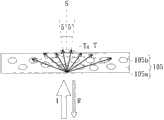
图2是根据图1所绘示的入射光通过光学结构层的光径示意图。FIG. 2 is a schematic diagram of an optical path of incident light passing through an optical structure layer according to FIG. 1 .
图3是根据本发明的较佳实施例所绘示的一种最适化有机电致发光元件的光取出率的方法流程图。FIG. 3 is a flow chart of a method for optimizing the light extraction rate of an organic electroluminescent device according to a preferred embodiment of the present invention.
其中,附图标记:Among them, reference signs:
100:有机发光二极管元件 101:基材100: Organic light emitting diode element 101: Substrate
102:透明电极 103:有机发光结构102: Transparent Electrode 103: Organic Light-Emitting Structure
104:反射层 105:光学结构层104: Reflective layer 105: Optical structure layer
105a:基底材料层 105b:纳米粒子105a:
Haze:雾度 I:入射光Haze: Haze I: Incident light
R:反射率 S:法线R: Reflectivity S: Normal
T:全光穿透率 T0:部分光穿透率T: Total light transmittance T0: Partial light transmittance
S31:提供一个包含有基材、透明电极、有机发光结构以及反射层的有机电致发光元件。S31: Provide an organic electroluminescent element comprising a substrate, a transparent electrode, an organic light-emitting structure and a reflective layer.
S32:提供基底材料S32: Provide base material
S33:将多个纳米粒子分散于基底材料中,并调整纳米粒子的浓度S33: Disperse a plurality of nanoparticles in the base material, and adjust the concentration of the nanoparticles
S34:将含有纳米粒子的基底材料涂布于基材相对于透明电极的一侧,并控制基底材料的涂布厚度S34: Coating the base material containing nanoparticles on the side of the base material opposite to the transparent electrode, and controlling the coating thickness of the base material
S35:硬化基底材料S35: Hardened base material
具体实施方式Detailed ways
以下结合附图和具体实施例对本发明进行详细描述,但不作为对本发明的限定。The present invention will be described in detail below in conjunction with the accompanying drawings and specific embodiments, but not as a limitation of the present invention.
本发明的目的就是在提供一种具有高光取出率的有机电致发光元件及其光取出率的最适化方法,以解决现有的有机电致发光元件的外部光子效率不佳以及光取出率低落的问题。为让本发明的上述和其它目的、特征和优点能更明显易懂,下文特举数个有机发光二极管元件(但不以此为限)作为较佳实施例,并配合所附图式,其详细说明如下:The object of the present invention is to provide an organic electroluminescent element with a high light extraction rate and an optimization method for the light extraction rate thereof, so as to solve the poor external photon efficiency and the light extraction rate of the existing organic electroluminescent element. low problem. In order to make the above and other objects, features and advantages of the present invention more comprehensible, several organic light-emitting diode elements (but not limited thereto) are listed below as preferred embodiments, together with the accompanying drawings, of which The details are as follows:
请参照图1,图1是根据本发明的一较佳实施例所绘示的一种有机发光二极管元件100的结构剖面示意图。Please refer to FIG. 1 . FIG. 1 is a schematic cross-sectional view of an organic light
有机发光二极管元件100,包括:基材101、透明电极102、有机发光结构103、反射层104以及光学结构层105。其中,基材101为一透光材质,较佳的材料可以是玻璃、半导体材质(例如硅)、塑化材料或其它类似材质。在本实例之中基材101是一种玻璃基板。透明电极102位于基材101上,较佳可以是氧化铟锡(indium tin oxide,ITO)玻璃所构成的透明阳极层。The organic light
有机发光结构103则位于透明电极102上。在本发明的一些实施例中,有机发光结构103较佳为一有机发光二极管结构,其至少包含有(但不以此为限)空穴传输层(Hole Transporting Layer,HTL)、有机发光层(Organic EmittingLayer,EL)、电子传输层(Electron Transporting Layer,ETL)、以及电子注入层(Electron Injection Layer,EIL)。由于有机发光二极管结构已为本领域技术人员所现有,因此形成该结构的相关材质与方法并不在此赘述。The organic
反射层104位于有机发光结构103之上。在本发明的实施例之中,反射层104可以是一种金属阴极层,或是一种镀覆于一氧化铟锡层的金属层,用来作为有机发光二极管元件100的阴极。The
光学结构层105位于基材101相对于透明电极102的一侧。在本发明的实施例中,光学结构层105是一种复合材料层,包含由塑化聚合物、玻璃等高分子材料或其它类似材料所组成的基底材料层105a,以及多个分散于基底材料层105a中的纳米粒子105b。The
构成这些纳米粒子105b的材料包含,二氧化钛、氧化锌、氧化钇、铽钇铝石榴石、氧化铝、二氧化硅、碳酸钙、硫酸钡、二氧化锆或上述材料的任意组合。在本发明的一些实施例中,这些纳米粒子105b的平均粒径实质介于0.1μm到1μm之间。The materials constituting these
通过调整光学结构层105中纳米粒子105b的浓度以及基底材料层105a的厚度,可以使光学结构层105的雾度(Haze)、全光穿透率T及反射率R达到一特定数值。在本发明的一些实施例中,这些纳米粒子105b的重量百分浓度,较佳实质介于1至10之间;而基底材料层105a的厚度实质介于0.1mm至1cm之间。By adjusting the concentration of
通过调整光学结构层105中纳米粒子105b的浓度以及基底材料层105a的厚度,可以使光学结构层105的反射率和全光穿透率二者之合,与雾度及反射率三者的乘积(Haze×R×(R+T))实质介于20%至35%之间。较佳使雾度实质大于65%,且使反射率实质大于5%。By adjusting the concentration of
值得注意的是,目前国际间对于雾度定义存在有多种不同的规范,各个规范的量测架构与方法各有不同,以下将采用数学公式,并配合图2来对光学结构层105的雾度进行定义:It is worth noting that there are currently many different international standards for the definition of haze, and the measurement frameworks and methods of each standard are different. The following mathematical formulas will be used in conjunction with Figure 2 to measure the haze of the
请参照图2,图2是根据图1的入射光通过光学结构层105的光径示意图。其中I代表入射光(incident light);R代表入射光的反射率;T代表全光穿透率;T0代表偏离法线S±5°角的部分光穿透率。雾度可由下述数学公式表示之:Please refer to FIG. 2 . FIG. 2 is a schematic diagram of the optical path of the incident light passing through the
雾度(Haze)=[T-T0]/T。Haze (Haze) = [T-T0]/T.
若将此一光学结构层105贴附于基材101相对于透明电极102的一侧,可以使由有机发光结构103所出射,并穿过透明电极102的光线,产生均匀的散射效果,借此提升有机发光二极管元件100的外部光子效率及光取出率。在本发明的一些实施例中,将采用光学结构层105的有机发光二极管元件100,与未采用光学结构层105的现有有机电致发光元件作比较。可发现,使用光学结构层105至少可以使有机电致发光元件提升5%到55%的外部光子效率及光取出率。If this
另外,通过调整光学结构层105中纳米粒子105b的浓度以及基底材料层105a的厚度,可以使有机发光二极管元件100的外部光子效率及光取出率达到最佳化。请参照图3,图3是根据本发明的较佳实施例所绘示的一种最适化有机电致发光元件的光取出率的方法流程图。In addition, by adjusting the concentration of the
有机电致发光元件光取出率的最适化包括下述步骤:The optimization of the light extraction rate of the organic electroluminescent element includes the following steps:
如步骤S31所绘示:首先提供一个包含有基材101、透明电极102、有机发光结构103以及反射层104的有机发光二极管元件100(未包含光学结构层105)。其中,透明电极102位于基材101上;有机发光结构103位于透明电极102上;反射层104位于有机发光结构103之上。As shown in step S31 : firstly, an organic light emitting
接着,于基材101相对于透明电极102的一侧,形成光学结构层105。在本发明的较佳实施例中,光学结构层105的形成方式,包括先提供基底材料(如步骤S32所绘示);再将平均粒径实质介于0.1μm到1μm的多个纳米粒子105b分散于基底材料中,并调整纳米粒子105b的浓度(如步骤S33所绘示);之后,将含有这些纳米粒子105b的基底材料,涂布于基材101相对于透明电极102的一侧,并控制基底材料的涂布厚度(如步骤S34所绘示)。Next, an
最后硬化基底材料(如步骤S35所绘示),而形成具有雾度(Haze)、反射率(R)以及全光穿透率(T),且反射率和全光穿透率二者之合,与雾度及反射率三者的乘积(Haze×R×(R+T))实质介于20%至35%之间的基底材料层105a。Finally harden the base material (shown in step S35) to form a haze (Haze), reflectivity (R) and total light transmittance (T), and the combination of reflectivity and total light transmittance , and the product of the haze and reflectivity (Haze×R×(R+T)) is substantially between 20% and 35% of the
在本发明的一较佳实施例中,雾度较佳控制在实质大于65%的范围,而反射率R较佳则是控制在实质大于5%的范围。而构成这些纳米粒子105b的材料,选自于二氧化钛、氧化锌、氧化钇、铽钇铝石榴石、氧化铝、二氧化硅、碳酸钙、硫酸钡、二氧化锆以及上述任意组合所组成的一族群。In a preferred embodiment of the present invention, the haze is preferably controlled within a range substantially greater than 65%, and the reflectivity R is preferably controlled within a range substantially greater than 5%. The materials constituting these
根据上述实施例,本发明是将含有多个纳米粒子的光学结构层,结合于有机电致发光元件上。通过调整光学结构层中纳米粒子的浓度以及光学结构层的厚度,使光学结构层的雾度、全光穿透率及反射率达到一特定数值,借以提高有机电致发光元件的外部光子效率及光取出率,解决现有有机电致发光元件,严重的光线吸收问题,达成上述发明目的。According to the above-mentioned embodiments, the present invention combines the optical structure layer containing a plurality of nanoparticles on the organic electroluminescence element. By adjusting the concentration of nanoparticles in the optical structure layer and the thickness of the optical structure layer, the haze, total light transmittance and reflectivity of the optical structure layer can reach a specific value, so as to improve the external photon efficiency and The light extraction rate solves the serious problem of light absorption in existing organic electroluminescent elements, and achieves the above-mentioned purpose of the invention.
当然,本发明还可有其它多种实施例,在不背离本发明精神及其实质的情况下,熟悉本领域的技术人员可根据本发明作出各种相应的改变和变形,但这些相应的改变和变形都应属于本发明权利要求的保护范围。Certainly, the present invention also can have other various embodiments, without departing from the spirit and essence of the present invention, those skilled in the art can make various corresponding changes and deformations according to the present invention, but these corresponding changes All changes and modifications should belong to the protection scope of the claims of the present invention.
Claims (10)
Applications Claiming Priority (2)
| Application Number | Priority Date | Filing Date | Title |
|---|---|---|---|
| TW100120465ATW201251505A (en) | 2011-06-10 | 2011-06-10 | Organic light electroluminescent device with high light extraction and optimization method thereof |
| TW100120465 | 2011-06-10 |
Publications (1)
| Publication Number | Publication Date |
|---|---|
| CN102290532Atrue CN102290532A (en) | 2011-12-21 |
Family
ID=45336761
Family Applications (1)
| Application Number | Title | Priority Date | Filing Date |
|---|---|---|---|
| CN2011102123375APendingCN102290532A (en) | 2011-06-10 | 2011-07-22 | Organic electroluminescent element with high light extraction rate and optimization method thereof |
Country Status (2)
| Country | Link |
|---|---|
| CN (1) | CN102290532A (en) |
| TW (1) | TW201251505A (en) |
Cited By (3)
| Publication number | Priority date | Publication date | Assignee | Title |
|---|---|---|---|---|
| CN103050639A (en)* | 2012-11-16 | 2013-04-17 | 友达光电股份有限公司 | Organic electroluminescent element |
| CN104218154A (en)* | 2013-05-30 | 2014-12-17 | 海洋王照明科技股份有限公司 | Organic light emission diode device and fabrication method thereof |
| CN108845416A (en)* | 2018-06-30 | 2018-11-20 | 云谷(固安)科技有限公司 | Light path adjusts device and display device |
Families Citing this family (1)
| Publication number | Priority date | Publication date | Assignee | Title |
|---|---|---|---|---|
| US9843012B2 (en) | 2014-12-26 | 2017-12-12 | Industrial Technology Research Institute | Top emitting organic electroluminescent devices |
Citations (4)
| Publication number | Priority date | Publication date | Assignee | Title |
|---|---|---|---|---|
| JP2004164902A (en)* | 2002-11-11 | 2004-06-10 | Matsushita Electric Works Ltd | Organic electroluminescent element |
| CN1656626A (en)* | 2002-03-29 | 2005-08-17 | 通用电气公司 | Mechanically flexible organic electroluminescent device with directional light emission |
| CN101400492A (en)* | 2006-03-20 | 2009-04-01 | 三井化学株式会社 | Optical film and method for producing same |
| CN101978779A (en)* | 2008-03-26 | 2011-02-16 | 住友化学株式会社 | Organic electroluminescence element, lighting device, and display device |
- 2011
- 2011-06-10TWTW100120465Apatent/TW201251505A/enunknown
- 2011-07-22CNCN2011102123375Apatent/CN102290532A/enactivePending
Patent Citations (4)
| Publication number | Priority date | Publication date | Assignee | Title |
|---|---|---|---|---|
| CN1656626A (en)* | 2002-03-29 | 2005-08-17 | 通用电气公司 | Mechanically flexible organic electroluminescent device with directional light emission |
| JP2004164902A (en)* | 2002-11-11 | 2004-06-10 | Matsushita Electric Works Ltd | Organic electroluminescent element |
| CN101400492A (en)* | 2006-03-20 | 2009-04-01 | 三井化学株式会社 | Optical film and method for producing same |
| CN101978779A (en)* | 2008-03-26 | 2011-02-16 | 住友化学株式会社 | Organic electroluminescence element, lighting device, and display device |
Cited By (5)
| Publication number | Priority date | Publication date | Assignee | Title |
|---|---|---|---|---|
| CN103050639A (en)* | 2012-11-16 | 2013-04-17 | 友达光电股份有限公司 | Organic electroluminescent element |
| CN103050639B (en)* | 2012-11-16 | 2016-04-06 | 友达光电股份有限公司 | organic electroluminescent element |
| CN104218154A (en)* | 2013-05-30 | 2014-12-17 | 海洋王照明科技股份有限公司 | Organic light emission diode device and fabrication method thereof |
| CN108845416A (en)* | 2018-06-30 | 2018-11-20 | 云谷(固安)科技有限公司 | Light path adjusts device and display device |
| CN108845416B (en)* | 2018-06-30 | 2023-12-08 | 广州国显科技有限公司 | Optical path adjusting device and display device |
Also Published As
| Publication number | Publication date |
|---|---|
| TW201251505A (en) | 2012-12-16 |
Similar Documents
| Publication | Publication Date | Title |
|---|---|---|
| TWI495175B (en) | Organic electroluminescent element | |
| EP2224788B1 (en) | Surface light source device | |
| TWI389597B (en) | Electroluminescent element and lighting device | |
| JP5703251B2 (en) | ORGANIC ELECTROLUMINESCENT ELEMENT, LIGHTING DEVICE, AND METHOD FOR PRODUCING ORGANIC ELECTROLUMINESCENT ELEMENT | |
| EP3018721B1 (en) | Substrate for organic light emitting device and organic light emitting device comprising same | |
| KR101654360B1 (en) | Substrate for oled and method for fabricating thereof | |
| US9793516B2 (en) | Light extraction substrate for organic light-emitting element, method for manufacturing same and organic light-emitting element including same | |
| CN108682753B (en) | OLED display panel and manufacturing method thereof | |
| CN102290532A (en) | Organic electroluminescent element with high light extraction rate and optimization method thereof | |
| KR101468972B1 (en) | Manufacturing method of substrate having light-scattering layer, substrate having light-scattering layer using the same, and oled including the substrate having light-scattering layer | |
| CN102386339B (en) | organic electroluminescent element | |
| CN105518896A (en) | Method for fabricating ultra-thin organic light-emitting device | |
| EP2720284B1 (en) | Method of fabricating a metal oxide thin film substrate for OLED | |
| US20170358763A1 (en) | Flexible substrate and method of manufacturing same | |
| WO2019085044A1 (en) | Oled display device and preparation method therefor | |
| CN102201545A (en) | Organic light-emitting device | |
| US10094534B2 (en) | Surface-emitting unit having dimming regions | |
| US9515295B2 (en) | Light extraction substrate for organic light emitting device, fabrication method therefor and organic light emitting device including same | |
| CN102201544A (en) | Organic light-emitting device | |
| US20160312964A1 (en) | Surface Emitting Unit | |
| JP2010218738A (en) | Organic el element, display using it, and lighting system | |
| CN100403100C (en) | flat panel display device | |
| TWM472951U (en) | Structure of organic light emitting diode | |
| JP2015176734A (en) | Board for el element, el element, lighting device, display device and liquid crystal display device | |
| CN203746913U (en) | Organic Light Emitting Diode Structure |
Legal Events
| Date | Code | Title | Description |
|---|---|---|---|
| C06 | Publication | ||
| PB01 | Publication | ||
| C10 | Entry into substantive examination | ||
| SE01 | Entry into force of request for substantive examination | ||
| C02 | Deemed withdrawal of patent application after publication (patent law 2001) | ||
| WD01 | Invention patent application deemed withdrawn after publication | Application publication date:20111221 |